JP2005197353A - Solid-state imaging device - Google Patents
Solid-state imaging device Download PDFInfo
- Publication number
- JP2005197353A JP2005197353A JP2004000359A JP2004000359A JP2005197353A JP 2005197353 A JP2005197353 A JP 2005197353A JP 2004000359 A JP2004000359 A JP 2004000359A JP 2004000359 A JP2004000359 A JP 2004000359A JP 2005197353 A JP2005197353 A JP 2005197353A
- Authority
- JP
- Japan
- Prior art keywords
- well
- source
- region
- source region
- substrate
- Prior art date
- Legal status (The legal status is an assumption and is not a legal conclusion. Google has not performed a legal analysis and makes no representation as to the accuracy of the status listed.)
- Withdrawn
Links
- 238000003384 imaging method Methods 0.000 title claims abstract description 24
- 239000000758 substrate Substances 0.000 claims abstract description 55
- 239000012535 impurity Substances 0.000 claims abstract description 42
- 230000015572 biosynthetic process Effects 0.000 claims abstract description 34
- 238000006243 chemical reaction Methods 0.000 claims abstract description 13
- 239000011229 interlayer Substances 0.000 claims description 18
- 229910021420 polycrystalline silicon Inorganic materials 0.000 claims description 13
- 229920005591 polysilicon Polymers 0.000 claims description 13
- 239000000463 material Substances 0.000 claims description 12
- 239000007769 metal material Substances 0.000 claims description 7
- 230000001747 exhibiting effect Effects 0.000 claims description 2
- 239000010410 layer Substances 0.000 description 42
- 238000009792 diffusion process Methods 0.000 description 21
- 238000009826 distribution Methods 0.000 description 13
- 238000010586 diagram Methods 0.000 description 10
- 238000005468 ion implantation Methods 0.000 description 10
- 238000000034 method Methods 0.000 description 10
- 238000002513 implantation Methods 0.000 description 9
- 238000004519 manufacturing process Methods 0.000 description 8
- OAICVXFJPJFONN-UHFFFAOYSA-N Phosphorus Chemical compound [P] OAICVXFJPJFONN-UHFFFAOYSA-N 0.000 description 7
- 229910052698 phosphorus Inorganic materials 0.000 description 7
- 239000011574 phosphorus Substances 0.000 description 7
- 238000005036 potential barrier Methods 0.000 description 6
- 239000011159 matrix material Substances 0.000 description 4
- 230000003287 optical effect Effects 0.000 description 4
- 238000009825 accumulation Methods 0.000 description 3
- 230000000694 effects Effects 0.000 description 3
- 238000005530 etching Methods 0.000 description 3
- 238000002955 isolation Methods 0.000 description 3
- 239000002344 surface layer Substances 0.000 description 3
- 230000005684 electric field Effects 0.000 description 2
- 230000005669 field effect Effects 0.000 description 2
- WFKWXMTUELFFGS-UHFFFAOYSA-N tungsten Chemical compound [W] WFKWXMTUELFFGS-UHFFFAOYSA-N 0.000 description 2
- 229910052721 tungsten Inorganic materials 0.000 description 2
- 239000010937 tungsten Substances 0.000 description 2
- RTAQQCXQSZGOHL-UHFFFAOYSA-N Titanium Chemical compound [Ti] RTAQQCXQSZGOHL-UHFFFAOYSA-N 0.000 description 1
- NRTOMJZYCJJWKI-UHFFFAOYSA-N Titanium nitride Chemical compound [Ti]#N NRTOMJZYCJJWKI-UHFFFAOYSA-N 0.000 description 1
- 229910052785 arsenic Inorganic materials 0.000 description 1
- RQNWIZPPADIBDY-UHFFFAOYSA-N arsenic atom Chemical compound [As] RQNWIZPPADIBDY-UHFFFAOYSA-N 0.000 description 1
- 229910052796 boron Inorganic materials 0.000 description 1
- -1 boron ions Chemical class 0.000 description 1
- 239000003990 capacitor Substances 0.000 description 1
- 230000001413 cellular effect Effects 0.000 description 1
- 239000004020 conductor Substances 0.000 description 1
- 238000001514 detection method Methods 0.000 description 1
- 238000007599 discharging Methods 0.000 description 1
- 230000003628 erosive effect Effects 0.000 description 1
- 150000002500 ions Chemical class 0.000 description 1
- 230000003647 oxidation Effects 0.000 description 1
- 238000007254 oxidation reaction Methods 0.000 description 1
- 238000002161 passivation Methods 0.000 description 1
- 239000010936 titanium Substances 0.000 description 1
- 229910052719 titanium Inorganic materials 0.000 description 1
- WQJQOUPTWCFRMM-UHFFFAOYSA-N tungsten disilicide Chemical compound [Si]#[W]#[Si] WQJQOUPTWCFRMM-UHFFFAOYSA-N 0.000 description 1
- 229910021342 tungsten silicide Inorganic materials 0.000 description 1
Images



Landscapes
- Solid State Image Pick-Up Elements (AREA)
- Transforming Light Signals Into Electric Signals (AREA)
Abstract
【課題】ソース領域へのリーク電流経路となるジャンクショントランジスタが構成されることを防止する。
【解決手段】 光電変換素子PDと該光電変換素子に隣接して形成されたトランジスタTMとを含む固体撮像装置において、一導電型の基板1と、前記光電変換素子の形成領域の前記基板1に形成された逆導電型の第1ウェル21と、前記第1ウェル21上に形成された一導電型の第2ウェル4と、前記トランジスタの形成領域の前記基板1に形成され、前記第1ウェル21に隣接して形成された逆導電型の第3ウェル21’と、前記第3ウェル21’上に形成され、前記第2ウェル4に隣接して形成された一導電型の第4ウェル5と、前記第4ウェル5上方に形成された、開口部を有するゲート電極6と、前記開口部下方に形成されたソース7と、前記ソース7と離間して形成され、前記第3ウェル21’に電気的に接続されたドレイン8と、を含み、前記ソース7の不純物濃度は、前記第3ウェル21’から前記ソース7へのリーク電流の経路が形成されないような濃度に設定されることを特徴とする。
【選択図】 図1
A junction transistor that serves as a leakage current path to a source region is prevented from being configured.
In a solid-state imaging device including a photoelectric conversion element PD and a transistor TM formed adjacent to the photoelectric conversion element, one conductivity type substrate 1 and the substrate 1 in the formation region of the photoelectric conversion element are provided. The first well 21 of opposite conductivity type formed, the second well 4 of one conductivity type formed on the first well 21, and the first well formed on the substrate 1 in the transistor formation region. A third well 21 ′ of opposite conductivity type formed adjacent to 21, and a fourth well 5 of one conductivity type formed on the third well 21 ′ and adjacent to the second well 4. A gate electrode 6 having an opening formed above the fourth well 5, a source 7 formed below the opening, and spaced apart from the source 7, and the third well 21 ' A drain 8 electrically connected to In addition, the impurity concentration of the source 7 is set to a concentration that does not form a leakage current path from the third well 21 ′ to the source 7.
[Selection] Figure 1
Description
本発明は、高画質特性及び低消費電力特性を有する固体撮像装置に関する。 The present invention relates to a solid-state imaging device having high image quality characteristics and low power consumption characteristics.
携帯電話などに搭載される固体撮像装置として、CCD(電荷結合素子)型のイメージセンサと、CMOS型のイメージセンサと、がある。CCD型のイメージセンサは画質に優れ、CMOS型のイメージセンサは消費電力が少なく、プロセスコストが低い。近年、高画質と低消費電力とを共に兼ね備えた閾値電圧変調方式のMOS型固体撮像装置が提案されている。閾値電圧変調方式のMOS型固体撮像装置については、例えば、特許文献1に開示されている。
As a solid-state imaging device mounted on a cellular phone or the like, there are a CCD (charge coupled device) type image sensor and a CMOS type image sensor. A CCD type image sensor has excellent image quality, and a CMOS type image sensor has low power consumption and low process cost. In recent years, a MOS type solid-state imaging device of a threshold voltage modulation method that has both high image quality and low power consumption has been proposed. A threshold voltage modulation type MOS solid-state imaging device is disclosed in, for example,
イメージセンサは、センサセルをマトリクス状に配列し、初期化、蓄積、読み出しの3つの状態を繰り返すことで、画像出力を得ている。特許文献1によって開示されたイメージセンサは、各単位画素が、蓄積を行うための受光ダイオードと、読み出しを行うためのトランジスタとを有している。
The image sensor obtains an image output by arranging sensor cells in a matrix and repeating three states of initialization, accumulation, and readout. In the image sensor disclosed in
図12は特許文献1に開示されているイメージセンサを示す模式的断面図である。
FIG. 12 is a schematic cross-sectional view showing the image sensor disclosed in
図12のイメージセンサは、基板100上において、各単位画素毎に、受光ダイオード111と絶縁ゲート型電界効果トランジスタ112とが隣接配置されている。トランジスタ112のゲート電極113はリング状に形成されており、ゲート電極113の中央の開口部分には、ソース領域114が形成されている。ゲート電極113の周辺にはドレイン領域115が形成されている。
In the image sensor of FIG. 12, a
受光ダイオード111の開口領域から入射した光によって発生した電荷(光発生電荷)は、ゲート電極113下方のP型のウェル領域116に転送されて、この部分に形成されたキャリアポケット117に蓄積される。キャリアポケット117に蓄積された光発生電荷によってトランジスタ112の閾値電圧が変化する。これにより、入射光に対応した信号(画素信号)を、トランジスタ112のソース領域114から取り出すことができるようになっている。
Charges (photogenerated charges) generated by light incident from the opening region of the
なお、特許文献1の装置では、同一列に配列された単位画素の出力は、共通のソース線を介して取り出されるようになっている。トランジスタ112のゲートに印加する電圧をライン毎に制御することで、共通のソース線に接続された各単位画素のうち所定のラインの単位画素からの選択的な読み出しを可能にしている。即ち、読み出しを行う単位画素(選択画素)のトランジスタ112には比較的高いゲート電圧を印加し、他の読み出しを行わない単位画素(非選択画素)のトランジスタ112には比較的低いゲート電圧を印加する。高いゲート電圧を印加したトランジスタの出力の方が低いゲート電圧を印加したトランジスタの出力よりも高く、ソース線から選択画素の出力を得ることができる。
ところで、図12の単位画素のソース領域114形成工程においては、不純物として例えばリンを注入する。ところが、リンは拡散係数が高いことから、高濃度のソース領域形成のためのイオン注入によって、ソース領域114下方のウェル領域116の一部(斜線領域)までリンが拡散されてしまう。即ち、ソース領域114によってウェル領域116が侵食されてしまい、侵食された部分とその隣接部分とによる破線にて囲った領域122において、ジャンクション電界効果トランジスタ(以下、ジャンクションFETともいう)が形成されてしまう。
Incidentally, in the step of forming the
なお、不純物として例えばヒ素のようなより質量数の大きい不純物を注入することで、ソース領域を浅く形成することが可能であるが、その場合注入時のダメージが極めて大きいことから、ソース領域形成には質量数の大きい不純物を用いることはできない。 It is possible to form a shallow source region by injecting an impurity having a larger mass number such as arsenic as an impurity. However, in this case, since the damage at the time of implantation is extremely large, the source region is formed. Cannot use impurities with a large mass number.
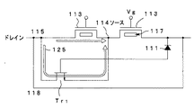
図13は図12の単位画素の等価回路を示す説明図である。ゲート電極113周辺のドレイン領域115とN型の拡散層118とは電気的に接続されており、図13に示すように、ドレイン領域115からN型拡散層118にいたるリーク経路125が形成される。N型拡散層118とソース領域114との間には、領域122においてJFET(図13のジャンクショントランジスタTr1)が形成されている。
FIG. 13 is an explanatory diagram showing an equivalent circuit of the unit pixel of FIG. The
図14は横軸に基板深さをとり縦軸に不純物濃度をとって、ソース領域114及びその下方のウェル領域116における濃度分布を示すグラフである。
FIG. 14 is a graph showing the concentration distribution in the
図14の曲線aはウェル領域116形成時の不純物注入による不純物濃度分布を示している。曲線aは、不純物を基板表面から若干離間したウェル領域116形成位置に対応した深さに注入したことを示している。これにより、ウェル領域116の拡散層118近傍における不純物濃度は比較的高い値となっている。
A curve a in FIG. 14 shows an impurity concentration distribution by impurity implantation when the
曲線bはソース領域114形成時の不純物注入による不純物濃度分布を示している。基板表面近傍にソース領域114を形成するようにイオン注入が行われる。しかし、上述したように、ソース領域形成時のイオン注入によって不純物は比較的深い領域まで拡散する。これにより、ソース領域114の不純物濃度分布は、図14の曲線cに示すものに変化する。曲線a,cの比較から明らかなように、ウェル領域116はソース領域114の下方領域において、ソース領域形成のための不純物の影響によって濃度が低下する。
A curve b represents an impurity concentration distribution by impurity implantation when the
なお、ソース領域114下方以外の領域のウェル領域116では、ソース領域114によるこのような侵食は生じない。つまり、ゲート電極113直下に形成したキャリアポケット117及びその下方のウェル領域116は高い濃度のP型で形成されるのに対し、ソース領域114の下方のウェル領域116は侵食されてしまい、侵食された部分とそれに隣接する濃いP型のウェル領域116とによってジャンクションFETが形成される。
Note that such erosion by the
曲線cに示すように、ソース領域114の下方のウェル領域116は電位障壁が著しく低下し、トランジスタ112が導通していない場合でも、ジャンクションFET(Tr1)は導通して、リーク経路125はドレイン領域115からソース領域114まで導通状態となる。このように、特許文献1の装置では、トランジスタ112が導通していない場合でも、ドレイン領域115とソース領域114との間にJFETによるリーク経路125が形成される。
As shown by the curve c, the
このため、トランジスタ112の特性は、特にゲート電圧Vgが比較的低いレベルの領域において、リーク電流の影響を受けてしまう。このリーク電流の影響によって、非選択画素の出力が大きくなり、正確な受光量を検出することができなくなってしまうことがある。例えば、一部に強い光が入射した場合には、この強い光の入射光の影響によって黒く表示される縦筋ノイズ(以下黒スミア)が発生してしまうことがあるという問題点があった。
Therefore, the characteristics of the
本発明はかかる問題点に鑑みてなされたものであって、ジャンクショントランジスタが形成されることを防止して、変調トランジスタの特性を改善し、高画質化を図ることができる固体撮像装置を提供することを目的とする。 The present invention has been made in view of such problems, and provides a solid-state imaging device capable of preventing the formation of a junction transistor, improving the characteristics of a modulation transistor, and achieving high image quality. For the purpose.
本発明に係る固体撮像装置は、光電変換素子と該光電変換素子に隣接して形成されたトランジスタとを含む固体撮像装置において、一導電型の基板と、前記光電変換素子の形成領域の前記基板に形成された逆導電型の第1ウェルと、前記第1ウェル上に形成された一導電型の第2ウェルと、前記トランジスタの形成領域の前記基板に形成され、前記第1ウェルに隣接して形成された逆導電型の第3ウェルと、前記第3ウェル上に形成され、前記第2ウェルに隣接して形成された一導電型の第4ウェルと、前記第4ウェル上方に形成された、開口部を有するゲート電極と、前記開口部下方に形成されたソースと、前記ソースと離間して形成され、前記第3ウェルに電気的に接続されたドレインと、を含み、前記ソースの不純物濃度は、前記第3ウェルから前記ソースへのリーク電流の経路が形成されないような濃度に設定されることを特徴とする。 The solid-state imaging device according to the present invention is a solid-state imaging device including a photoelectric conversion element and a transistor formed adjacent to the photoelectric conversion element, and a substrate of one conductivity type and the substrate in the formation region of the photoelectric conversion element. A first well of opposite conductivity type formed on the first well, a second well of one conductivity type formed on the first well, and formed on the substrate in the formation region of the transistor, adjacent to the first well. A reverse conductivity type third well formed on the third well, and a one conductivity type fourth well formed adjacent to the second well, and formed above the fourth well. A gate electrode having an opening; a source formed below the opening; and a drain formed spaced apart from the source and electrically connected to the third well. The impurity concentration is the third Wherein the path of the leakage current to the source from E Le is set to a concentration as not formed.
このような構成によれば、光電変換素子形成領域の第1ウェルに発生した光発生電荷は、第2ウェルから第4ウェルに転送される。第4ウェルに保持された光発生電荷によってトランジスタのチャネルの閾値電圧が制御されて、前記光発生電荷に応じた画素信号がトランジスタから出力される。トランジスタのソース領域は逆導電型で構成され、トランジスタの形成領域には、一導電型の第4ウェル及び逆導電型の第3ウェルが形成される。しかし、ソースの不純物濃度は、第3ウェルからソースへのリーク電流の経路が形成されないような濃度に設定される。これにより、高画質化を図ることができ、例えば、黒スミアの発生を防止することができる。 According to such a configuration, the photo-generated charges generated in the first well in the photoelectric conversion element formation region are transferred from the second well to the fourth well. The threshold voltage of the channel of the transistor is controlled by the photogenerated charge held in the fourth well, and a pixel signal corresponding to the photogenerated charge is output from the transistor. The source region of the transistor is constituted by a reverse conductivity type, and a first conductivity type fourth well and a reverse conductivity type third well are formed in the transistor formation region. However, the impurity concentration of the source is set so as not to form a leakage current path from the third well to the source. Thereby, high image quality can be achieved, and for example, occurrence of black smear can be prevented.
また、前記ソースの濃度は、前記ソース領域のコンタクト材料として金属材料を用いた場合には、非オーミック性を呈する濃度であることを特徴とする。 Further, the concentration of the source is a concentration exhibiting non-ohmic properties when a metal material is used as a contact material of the source region.
このような構成によれば、ソース領域の濃度が十分に低いので、ソース領域下方の一方導電型の不純物濃度を確実に所定の濃度以上に維持することができる。 According to such a configuration, since the concentration of the source region is sufficiently low, it is possible to reliably maintain the impurity concentration of one conductivity type below the source region at a predetermined concentration or more.
また、本発明に係る固体撮像装置は、前記基板上方に形成される層間絶縁膜と、前記ソース上の前記層間絶縁膜に形成されたコンタクトホールと、前記コンタクトホールに埋め込まれたポリシリコンと、を具備することを特徴とする。 The solid-state imaging device according to the present invention includes an interlayer insulating film formed above the substrate, a contact hole formed in the interlayer insulating film on the source, polysilicon buried in the contact hole, It is characterized by comprising.
このような構成によれば、ソース領域と層間絶縁膜上に形成される例えば配線層とを電気的に接続する配線材料としてポリシリコンが用いられる。ポリシリコンをコンタクト材料として用いることで、ソース領域の濃度が所定の濃度以下の低い濃度である場合でも、オーミック性を維持することができる。 According to such a configuration, polysilicon is used as a wiring material for electrically connecting, for example, a wiring layer formed on the source region and the interlayer insulating film. By using polysilicon as a contact material, ohmic properties can be maintained even when the concentration of the source region is a low concentration equal to or lower than a predetermined concentration.
以下、図面を参照して本発明の実施の形態について詳細に説明する。図1乃至図9は本発明の第1の実施の形態に係り、図1は本実施の形態に係る固体撮像装置の断面形状を示す断面図、図2は本実施の形態に係る固体撮像装置の1センサセルの平面形状を示す平面図、図3は本実施の形態におけるコンタクトの構成を説明するための説明図である。図4は素子の全体構造を等価回路によって示す回路ブロック図である。図5は黒スミアの発生理由を説明するためのグラフである。図6は横軸に基板深さをとり縦軸に不純物濃度をとって、ソース領域及びその下方における濃度分布を説明するためのグラフである。図7は本実施の形態における固体撮像装置中の変調トランジスタの特性を示すグラフである。図8及び図9は素子の製造方法を説明するための工程図である。 Hereinafter, embodiments of the present invention will be described in detail with reference to the drawings. 1 to 9 relate to a first embodiment of the present invention, FIG. 1 is a sectional view showing a sectional shape of a solid-state imaging device according to the present embodiment, and FIG. 2 is a solid-state imaging device according to the present embodiment. FIG. 3 is an explanatory diagram for explaining a configuration of a contact in the present embodiment. FIG. 4 is a circuit block diagram showing the entire structure of the element by an equivalent circuit. FIG. 5 is a graph for explaining the reason for the occurrence of black smear. FIG. 6 is a graph for explaining the concentration distribution in the source region and below, with the horizontal axis representing the substrate depth and the vertical axis representing the impurity concentration. FIG. 7 is a graph showing the characteristics of the modulation transistor in the solid-state imaging device according to the present embodiment. 8 and 9 are process diagrams for explaining a method for manufacturing the element.
<センサセルの構造>
本実施の形態における固体撮像装置は、単位画素であるセンサセルがマトリクス状に配列されて構成されたセンサセルアレイを有している。各センサセルは、入射光に応じて発生させた光発生電荷を収集・蓄積し、蓄積した光発生電荷に基づくレベルの画素信号を出力する。センサセルをマトリクス状に配列することで1画面の画像信号が得られる。
<Structure of sensor cell>
The solid-state imaging device according to the present embodiment has a sensor cell array in which sensor cells that are unit pixels are arranged in a matrix. Each sensor cell collects and accumulates photogenerated charges generated according to incident light, and outputs a pixel signal at a level based on the accumulated photogenerated charges. An image signal of one screen can be obtained by arranging the sensor cells in a matrix.
先ず、図1及び図2を参照して各センサセルの構造について説明する。図2は1つのセンサセルを示している。また、本実施の形態は光発生電荷として正孔を用いる例を示している。光発生電荷として電子を用いる場合でも同様に構成可能である。なお、図1は図2のA−A’線で切断したセルの断面構造を示している。 First, the structure of each sensor cell will be described with reference to FIGS. FIG. 2 shows one sensor cell. This embodiment shows an example in which holes are used as photogenerated charges. Even in the case where electrons are used as the photo-generated charges, the same configuration is possible. FIG. 1 shows a cross-sectional structure of the cell cut along the line A-A ′ of FIG. 2.
図2の平面図に示すように、単位画素であるセンサセル3内に、フォトダイオードPDと変調トランジスタTMとが隣接して設けられている。変調トランジスタTMとしては、例えば、NチャネルディプレッションMOSトランジスタが用いられる。単位画素は例えば長方形状を有している。
As shown in the plan view of FIG. 2, a photodiode PD and a modulation transistor TM are provided adjacent to each other in a
光電変換素子形成領域であるフォトダイオードPD形成領域においては、基板1の表面に開口領域2が形成され、基板1表面の比較的浅い位置には開口領域2よりも広い領域のP型のウェルであり、光電変換素子によって発生した光発生電荷を収集する第2ウェルとしての収集ウェル4が形成されている。収集ウェル4上には基板1の表面に、ピニング層としてのN型の拡散層32が形成されている。
In the photodiode PD formation region which is a photoelectric conversion element formation region, an
収集ウェル4に所定の距離だけ離間して、変調トランジスタTM形成領域にP型のウェルであり、収集ウェル4に収集された光発生電荷が転送されて変調トランジスタTMを制御するための第4ウェルとしの変調用ウェル5が形成されている。
A fourth well that is spaced apart from the collection well 4 by a predetermined distance, is a P-type well in the modulation transistor TM formation region, and controls the modulation transistor TM by transferring the photogenerated charges collected in the collection well 4 The
変調用ウェル5上には、基板1表面にリング状のゲート(リングゲート)6が形成されており、リングゲート6の中央の開口部分の基板1表面近傍領域には、濃度が比較的低いN型のソース領域7が形成されている。リングゲート6の周囲にはN型のドレイン領域8が形成されている。ドレイン領域8の所定位置には、基板1表面近傍にN+層のドレインコンタクト領域(図示せず)が形成される。
On the modulation well 5, a ring-shaped gate (ring gate) 6 is formed on the surface of the
変調用ウェル5は変調トランジスタTMのチャネルの閾値電圧を制御するものである。変調用ウェル5内には、リングゲート6の下方にP型の高濃度領域であるキャリアポケット10(図1)が形成されている。変調トランジスタTMは、変調用ウェル5、リングゲート6、ソース領域7及びドレイン領域8によって構成されて、変調用ウェル5(キャリアポケット10)に蓄積された電荷に応じてチャネルの閾値電圧が変化するようになっている。
The modulation well 5 controls the threshold voltage of the channel of the modulation transistor TM. In the modulation well 5, a carrier pocket 10 (FIG. 1) that is a P-type high concentration region is formed below the
ドレイン領域8及び拡散層32がドレイン電圧の印加によって正の電位にバイアスされることによって、フォトダイオードPDの開口領域2下方においては、拡散層32と収集ウェル4との境界面から空乏層が収集ウェル4の全体に広がって第1ウェルであるN型ウェル21に達する。一方、基板1とN型ウェル21との境界面から空乏層がN型ウェル21全体に広がって、収集ウェル4に達する。空乏領域において、開口領域2を介して入射した光による光発生電荷が生じる。そして、上述したように、発生した光発生電荷は収集ウェル4に収集されるようになっている。
When the
収集ウェル4に収集された電荷は、変調用ウェル5に転送されてキャリアポケット10に保持される。これにより、変調トランジスタTMのソース電位は、変調用ウェル5に転送された電荷の量、即ち、フォトダイオードPDへの入射光に応じたものとなる。
The charges collected in the collection well 4 are transferred to the modulation well 5 and held in the
<センサセルの断面>
更に、図1を参照して、センサセル3の断面構造を詳細に説明する。
<Sensor cell cross section>
Furthermore, the cross-sectional structure of the
図1は1単位画素(セル)を構成するフォトダイオードPD形成領域と変調トランジスタTM形成領域とを示している。隣接するセル同士のフォトダイオードPD形成領域と変調トランジスタTM形成領域との間にアイソレーション領域22が設けられている。
FIG. 1 shows a photodiode PD formation region and a modulation transistor TM formation region constituting one unit pixel (cell). An
基板1の比較的深い位置には、P型基板1の全域にN型ウェル21が形成されている。フォトダイオード形成領域のN型ウェル21上には、P型の収集ウェル4が形成されている。収集ウェル4上の基板表面側には、ピニング層であるN型の拡散層32が形成されている。N型ウェル21は基板の比較的深い位置まで形成されている。
An N-
一方、変調トランジスタTM形成領域においては、基板1上にP型埋込層23が形成されている。P型埋込層23によって第3ウェルを構成するN型ウェル21’は基板の比較的浅い位置までに制限される。P型埋込層23上のN型ウェル21’上には、P型の変調用ウェル5が形成されている。変調用ウェル5内には、P+拡散によるキャリアポケット10が形成されている。
On the other hand, a P-type buried
変調トランジスタTM形成領域においては、基板表面にゲート酸化膜31を介してリングゲート6が形成され、リングゲート6下の基板表面にはチャネルを構成するN型の拡散層27が形成される。リングゲート6の中央の基板表面にはN-拡散層が形成されてソース領域7を構成する。また、リングゲート6の周囲の基板表面にはN型拡散層が形成されてドレイン領域8を構成する。チャネルを構成するN型拡散層27はソース領域7とドレイン領域8とに接続される。
In the modulation transistor TM formation region, the
<基板表面の構成>
基板表面には層間絶縁膜33を介して配線層が形成され、配線層上には配線36が形成されている。層間絶縁膜33はソース領域7上において開孔されてコンタクトホール34が形成されている。本実施の形態においては、コンタクトホール34に埋め込まれるコンタクト材料として、ポリシリコン35が採用される。配線36はコンタクトホール34に埋め込まれたポリシリコン35によってソース領域7に電気的に接続されている。
<Configuration of substrate surface>
A wiring layer is formed on the substrate surface via an
なお、層間絶縁膜33上の配線層上には、更に、図示しない層間絶縁膜を介在させながら複数の層が形成されている。これらの各層としては、例えば配線層、遮光層、パシベーション層等がある。基板表面のコンタクト及び各層の導通材料は、各層間絶縁膜に開口したコンタクトホールを介して上層又は下層に電気的に接続されている。例えば、リングゲート6及びドレイン領域8等は、図示しないコンタクトホールに埋め込まれた金属材料によって、上層の配線層に接続されるようになっている。
A plurality of layers are further formed on the wiring layer on the
<第1の実施の形態の特徴>
本実施の形態においては、上述したように、ソース領域7は、比較的濃度が低いN-拡散層で構成されている。ソース領域7のN型の濃度が比較的低いことから、変調用ウェル5のP型の濃度は相対的には高いことになり、ソース領域7の形成時に変調用ウェル5は殆ど侵食されることはない。即ち、ソース領域7の下方領域28においても変調用ウェル5は十分に高い濃度に維持され、電子に対する高い電位障壁が得られる。また、下方領域28において、変調用ウェル5内に濃度分布の差によるジャンクションFETが形成されることを防止することができる。
<Characteristics of the first embodiment>
In the present embodiment, as described above, the
ところで、一般的には、ソース領域7とのコンタクト材料としては、金属材料が用いられる。特許文献1等において開示されている従来の固体撮像装置においては、ソース領域は十分に濃い不純物濃度に設定される。この場合には、コンタクト材料として金属材料を用いることにより、十分に低いコンタクト抵抗が得られる。
In general, a metal material is used as a contact material with the
しかしながら、本実施の形態のようにソース領域7の濃度を薄くした場合には、ソース領域7と金属材料とのコンタクト抵抗は著しく増大し、非オーミック性を有することとなる。そこで、本実施の形態においては、コンタクト材料としてポリシリコンを採用することによって、比較的濃度が低いソース領域7とコンタクト材料であるポリシリコン35とのコンタクト抵抗を低下させ、十分なオーミック性を確保することを可能にしている。
However, when the concentration of the
図3はソース領域7とのコンタクトを説明するためのための説明図である。図3(a)及び図3(b)は参考としてリングゲート6の構造及び従来の一般的なソースコンタクトの構造を示し、図3(c)は本実施の形態におけるソースコンタクトの構造を示している。
FIG. 3 is an explanatory diagram for explaining a contact with the
図3(a)に示すように、リングゲート6は、基板1の表面に形成されたゲート酸化膜31上にポリシリコン6aを形成し、更に、ポリシリコン6a上にタングステンシリサイド6bを形成して構成される。従来のソースコンタクトは、図3(b)に示すように、基板1の表層に形成された高濃度N+拡散層によってソース領域114が形成される。基板1の表面には層間絶縁膜が形成され、層間絶縁膜にはコンタクトホール120が開孔されている。従来のソースコンタクトは、コンタクト材料として金属材料であるタングステン123を用いる。更に、タングステン123とソース領域114の表面との間に、窒化チタン121及びチタン122の層を積層するようになっている。
As shown in FIG. 3A, in the
これに対し、本実施の形態においては、図3(c)に示すように、基板1の表層に形成された比較的濃度が低いN-拡散層によってソース領域7が形成される。基板1の表面に形成された層間絶縁膜にはコンタクトホール34が開孔されている。上述したように、コンタクトホール34に埋め込むコンタクト材料としては、ポリシリコン35を用いる。ポリシリコン35をコンタクト材料として用いることによって、ソース領域7の濃度が比較的低い場合でも、コンタクト部のオーミック性を確保することができる。
On the other hand, in the present embodiment, as shown in FIG. 3C, the
なお、変調トランジスタTMはソース領域7の電圧値を検出することで画素信号を得ており、ソース領域7には電流が殆ど流れないことから、コンタクト材料をポリシリコン35にすることによって多少コンタクト抵抗が大きくなったとしても、特には問題は生じない。
Note that the modulation transistor TM obtains a pixel signal by detecting the voltage value of the
<装置全体の回路構成>
次に、図4を参照して本実施の形態に係る固体撮像装置全体の回路構成について説明する。
<Circuit configuration of the entire device>
Next, a circuit configuration of the entire solid-state imaging device according to the present embodiment will be described with reference to FIG.
固体撮像装置61は図2のセンサセル3を含むセンサセルアレイ62とセンサセルアレイ62中の各センサセル3を駆動する回路63〜65とを有している。センサセルアレイ62は、セル3をマトリクス状に配置して構成されている。センサセルアレイ62は、例えば、640×480のセル3と、オプティカルブラック(OB)のための領域(OB領域)を含む。OB領域を含めると、センサセルアレイ62は例えば712×500のセル3で構成される。
The solid-state imaging device 61 includes a
各センサセル3は、光電変換を行うフォトダイオードPDと、光信号を検出して読み出すための変調トランジスタTMとを含む。フォトダイオードPDは入射光に応じた電荷(光発生電荷)を生じさせ、生じた電荷は収集ウェル4(図4では接続点PDWに相当)内に収集される。収集ウェル4に収集された光発生電荷は、変調トランジスタTMの閾値変調用の変調用ウェル5(図4では接続点TMWに相当)内のキャリアポケット10に転送されて保持される。
Each
変調トランジスタTMは、キャリアポケット10に光発生電荷が保持されることでバックゲートバイアスが変化したことと等価となり、キャリアポケット10内の電荷量に応じてチャネルの閾値電圧が変化する。これにより、変調トランジスタTMのソース電圧は、キャリアポケット10内の電荷に応じたもの、即ち、フォトダイオードPDの入射光の明るさに対応したものとなる。
The modulation transistor TM is equivalent to a change in the back gate bias due to the photogenerated charge held in the
このように各セル3は、変調トランジスタTMのリングゲート6、ソース領域7及びドレイン領域8に駆動信号が印加されることで、蓄積、転送、読み出し及び排出等の動作を呈する。セル3の各部には図4に示すように、垂直駆動走査回路63、ドレイン駆動回路64及び水平駆動走査回路65から信号が供給されるようになっている。垂直駆動走査回路63は、各行のゲート線67に走査信号を供給し、ドレイン駆動回路64は各列のドレイン領域8にドレイン電圧を印加する。また、水平駆動走査回路65は、各ソース線66に接続されたスイッチ68に駆動信号を供給する。
In this manner, each
各セル3は、センサセルアレイ62に水平方向に配列された複数のソース線66と垂直方向に配列された複数のゲート線67との交点に対応して設けられている。水平方向に配列された各ラインの各セル3は、変調トランジスタTMのリングゲート6が共通のゲート線67に接続され、垂直方向に配列された各列の各セル3は、変調トランジスタTMのソースが共通のソース線66に接続される。
Each
複数のゲート線67の1つにオン信号(選択ゲート電圧)を供給することで、オン信号が供給されたゲート線67に共通接続された各セルが同時に選択されて、これらの選択されたセルの各ソースから各ソース線66を介して画素信号が出力される。垂直駆動走査回路63は1フレーム期間においてゲート線67にオン信号を順次シフトさせながら供給する。オン信号が供給されたラインの各セルからの画素信号が1ライン分同時に各ソース線66から読み出されて各スイッチ68に供給される。1ライン分の画素信号は水平駆動走査回路65によって、スイッチ68から画素毎に順次出力(ライン出力)される。
By supplying an ON signal (selection gate voltage) to one of the plurality of
各ソース線66に接続されたスイッチ68は、共通の定電流源(負荷回路)69を介して映像信号出力端子70に接続されている。各センサセル3の変調トランジスタTMのソースは定電流源69に接続されることになり、センサセル3のソースフォロワ回路が構成される。
The switch 68 connected to each source line 66 is connected to the video
<作用>
上述した特許文献1の装置においても、同一列の全ての変調トランジスタのソース領域を共通接続して、選択行と非選択行とで変調トランジスタのゲートに印加する電圧を制御することで、所望の行の変調トランジスタのソース電圧を検出するようになっている。即ち、選択行の全画素について、ゲート電極の電位(Vg)を高く設定し、非選択行のゲート電極の電位(Vg)を接地電位とする。
<Action>
In the device of
また、各単位画素同士のばらつきや、各種ノイズの除去のために、読出し動作において、選択行の光信号の読出し動作に続いて、非選択行の画素への電位付与状態はそのままにして、その選択行の画素を初期化し、引き続き、初期化した状態での閾値電圧を読み出す。そして、光発生電荷量に対応する閾値電圧と初期化した状態での閾値電圧の差の信号を算出し、正味の光信号成分を映像信号として出力する。 In addition, in order to eliminate variations between unit pixels and various noises, in the read operation, following the read operation of the optical signal of the selected row, the potential application state to the pixels of the non-selected row is left as it is. The pixels in the selected row are initialized, and subsequently the threshold voltage in the initialized state is read out. Then, a signal of the difference between the threshold voltage corresponding to the photogenerated charge amount and the threshold voltage in the initialized state is calculated, and the net optical signal component is output as a video signal.
特許文献1の装置における読み出し処理を変調トランジスタTMの特性を示す図5を用いて説明する。図5の特性A’〜D’は夫々暗時、通常の光の入射時、極めて強い光の入射時及びクリア時における変調トランジスタTMの特性を示している。
A reading process in the apparatus of
図5において、ポイントa,bは夫々通常レベルの入射光が入射した選択行の画素に基づく画素信号のレベル及びその初期化後のノイズ成分による画素信号のレベルVsa,Vnbを示している。また、ポイントcは極めて明るい入射光が入射した非選択行の画素に基づく画素信号のレベルVcを示している。通常の強さの光が入射した場合には、選択行の画素の画素信号として、レベルが(Vsa−Vnb)(矢印の範囲)の信号が得られる。 In FIG. 5, points a and b indicate pixel signal levels based on pixels in the selected row where normal level incident light is incident and pixel signal levels Vsa and Vnb based on the noise components after initialization. Point c indicates the level Vc of the pixel signal based on the pixel in the non-selected row where the extremely bright incident light is incident. When light of normal intensity is incident, a signal having a level of (Vsa−Vnb) (arrow range) is obtained as the pixel signal of the pixel in the selected row.
いま、所定の列において、選択行の画素には通常レベルの入射光が入射し、非選択行の画素の1つに極めて明るい入射光が入射するものとする。選択行の画素に基づく初期化前の画素信号のレベルはVsaとなる。しかし、選択行の初期化後の画素信号のレベルVnbは、極めて強い光が入射した場合の非選択行の画素に基づく画素信号のレベルVcよりも低い。同一列ではソース領域は共通接続されていることから、初期化後の読み出し時には、より高いレベルVcが初期化後の画素信号のレベルとして得られる。即ち、選択行の画素の画素信号として、レベルが(Vsa−Vc)の信号が出力されることになる。(Vsa−Vc)は比較的小さい値であり、この画素信号出力に基づく表示は黒くなる。極めて強い光が入射した画素の初期化が行われるまでは、当該ソース線66に接続された各画素の出力は、全て比較的小さい値となって、画面表示は垂直方向の黒スミアとなる。 Now, in a predetermined column, it is assumed that normal level incident light is incident on the pixels in the selected row and extremely bright incident light is incident on one of the pixels in the non-selected rows. The level of the pixel signal before initialization based on the pixels in the selected row is Vsa. However, the level Vnb of the pixel signal after initialization of the selected row is lower than the level Vc of the pixel signal based on the pixels of the non-selected row when extremely strong light is incident. Since the source regions are commonly connected in the same column, a higher level Vc is obtained as the pixel signal level after initialization at the time of readout after initialization. That is, a signal having a level (Vsa−Vc) is output as the pixel signal of the pixel in the selected row. (Vsa−Vc) is a relatively small value, and the display based on the pixel signal output is black. Until initialization of a pixel to which extremely intense light is incident is performed, the output of each pixel connected to the source line 66 is a relatively small value, and the screen display is a black smear in the vertical direction.
これに対し、本実施の形態においては、ソース領域7を比較的薄い濃度で形成することによって、強い光が入射した場合の黒スミアの発生を防止するようになっている。
On the other hand, in this embodiment, the
先ず、センサセル3のフォトダイオードPDの光検出及び光発生電荷の収集動作並びに変調トランジスタTMの読み出し動作について説明する。
First, the light detection and photogenerated charge collection operation of the photodiode PD of the
変調トランジスタTMのリングゲート6に低いゲート電圧を印加し、ドレイン領域8にトランジスタの動作に必要な例えば約2〜4Vの電圧(VDD)を印加する。これにより、N型ウェル21が空乏化する。また、ドレイン領域8とソース領域7との間に電界が生じる。
A low gate voltage is applied to the
フォトダイオードPDの開口領域2を介して入射した光が、空乏化したN型ウェル21に入射することで、電子−正孔対(光発生電荷)が生じる。P型の収集ウェル4は高濃度のP型不純物が導入されてポテンシャルが低くなっており、N型ウェル21に発生した光発生電荷は収集ウェル4に収集される。更に、光発生電荷は収集ウェル4から変調トランジスタ形成領域内の変調用ウェル5に転送されて、キャリアポケット10に蓄積される。
Light incident through the
キャリアポケット10に蓄積された光発生電荷によって、変調トランジスタTMの閾値電圧が変化する。この状態で、選択画素のリングゲート6に例えば約2〜4Vのゲート電圧(選択ゲート電圧)を印加し、ドレイン領域8に例えば約2〜4Vの電圧VDDを印加する。更に、変調トランジスタTMのソース領域7に定電流源69によって一定の電流を流す。これにより、変調トランジスタTMはソースフォロワ回路を形成し、光発生電荷による変調トランジスタTMの閾値電圧の変動に追随してソース電位が変化して、出力電圧が変化する。即ち、入射光に応じた出力が得られる。
The threshold voltage of the modulation transistor TM is changed by the photo-generated charges accumulated in the
初期化時には、キャリアポケット10、収集ウェル4及び変調用ウェル5内に残留する電荷を排出する。例えば、変調トランジスタTMのドレイン領域8及びリングゲート6に7〜8Vの高い正電圧を印加する。変調用ウェル5下方のN型ウェル21’の厚さは薄く、また、N型ウェル21’に面する基板1には高濃度のP型埋込層23が形成されているので、リングゲート6に印加した電圧による影響は変調用ウェル5及びその隣接領域にのみ作用する。即ち、変調用ウェル5に急激なポテンシャル変化が生じ、光発生電荷を基板1側に掃き出すような強い電界が主として変調用ウェル5に印加されて、残留した光発生電荷は、低いリセット電圧でより確実に基板1に排出される。
At the time of initialization, charges remaining in the
初期化後において、非選択画素のリングゲートには、比較的低い電圧値の非選択ゲート電圧を印加すると共に、選択画素のリングゲート6には比較的高い電圧値の選択ゲート電圧を印加する。そして、共通接続されたソース線66から、選択画素の初期化後の信号出力を得る。
After initialization, a non-selection gate voltage having a relatively low voltage value is applied to the ring gate of the non-selection pixel, and a selection gate voltage having a relatively high voltage value is applied to the
本実施の形態においては、ソース領域7は比較的薄い濃度で形成されている。従って、ソース領域7の形成時に変調用ウェル5が侵食されることが防止される。即ち、ソース領域7の下方領域28において、変調用ウェル5は充分に高い濃度に維持される。これにより、ソース領域7の下方には十分に高い電位障壁が形成されることになる。また、P型の変調用ウェル5内に濃度の変化が生じることはなく、ジャンクションFETが形成されることはない。これにより、N型ウェル21’からソース領域7への電流経路が形成されることはない。
In the present embodiment, the
図6はソース領域及びその下方における濃度分布を説明するためのものである。図6の曲線aはP型ウェル5形成時の不純物注入による不純物濃度分布を示している。曲線aは、不純物を基板表面から若干離間したP型ウェル5形成位置に対応した深さに注入したことを示している。
FIG. 6 is a diagram for explaining the source region and the concentration distribution below the source region. A curve a in FIG. 6 shows an impurity concentration distribution by impurity implantation when the P-
曲線dはソース領域7形成時の不純物注入による不純物濃度分布を示している。基板表面近傍にソース領域7を形成するようにイオン注入が行われる。ソース領域形成時のイオン注入によって不純物は形成しようとするソース領域7の深さよりも深い領域まで拡散する。しかしながら、本実施の形態においては、図14と図6との比較から明らかなように、ソース領域7は比較的薄い濃度で形成される。即ち、ソース領域7形成時の不純物の拡散は、比較的浅い位置でとどまり、また、不純物濃度が低いことから、P型の変調用ウェル5は殆ど侵食されない。結果的に、ソース領域7及びその下方の総合的な不純物濃度分布は、図6の曲線eに示すものとなる。
A curve d shows an impurity concentration distribution by impurity implantation when the
即ち、曲線eに示すように、ソース領域7の濃度を比較的薄く形成することによって、ソース領域7によって変調用ウェル5が侵食されることを防止し、ソース領域7の下方領域における不純物濃度を高いままに維持する。これにより、ソース領域7下方の下方領域28において、電子に対して十分高い電位障壁が得られる。
That is, as shown by the curve e, by forming the
また、ソース領域7下方において変調用ウェル5の水平方向には濃度分布の変化が小さく、ジャンクションFETが形成されることはない。こうして、変調トランジスタTMのトランジスタ特性を向上させることができる。
In addition, the change in the concentration distribution is small in the horizontal direction of the modulation well 5 below the
図7は本実施の形態におけるトランジスタ特性を示している。図7の特性Aは暗時におけるVg(ゲート電圧)−Vs(ソース電圧)特性を示し、特性Bは通常の光の入射時におけるVg−Vs特性を示し、特性Cは極めて強い光の入射時におけるVg−Vs特性を示し、特性Dはクリア時におけるVg−Vs特性を示している。 FIG. 7 shows transistor characteristics in this embodiment. Characteristic A in FIG. 7 shows the Vg (gate voltage) -Vs (source voltage) characteristic in the dark, characteristic B shows the Vg-Vs characteristic when normal light is incident, and characteristic C is when the extremely strong light is incident. The Vg-Vs characteristic is shown, and the characteristic D shows the Vg-Vs characteristic at the time of clearing.
下方領域28によって十分に高い電位障壁が得られ、ソース領域7の下方においてジャンクションFETが形成されないことから、N型ウェル21’からソース領域7へのリーク電流経路が形成されない。これにより、図7に示すように、比較的低いゲート電圧の範囲においても、変調トランジスタTMは、比較的直線性に優れたVg−Vs特性を有する。
Since the
図7に示すように、強い光が入射した非選択画素においても、十分に低い非選択ゲート電圧を印加した場合には、画素信号の出力レベルは初期化後の選択画素の画素信号レベルよりも低くなる。これにより、同一列の各画素が共通のソース線66に接続されている場合でも、十分に高い選択ゲート電圧を変調トランジスタTMのリングゲート6に印加することによって、初期化前後の画素信号として選択画素から得た画素信号を得ることができる。即ち、極めて強い光が入射した場合でも、通常の明るさの光が入射した場合と同様に、選択画素に基づく初期化前後の信号が得られることになり、入射光量に応じた正常な画素信号を出力することができ、黒スミアの発生を防止することができる。
As shown in FIG. 7, even in a non-selected pixel in which strong light is incident, when a sufficiently low non-selected gate voltage is applied, the output level of the pixel signal is higher than the pixel signal level of the selected pixel after initialization. Lower. Thereby, even when each pixel in the same column is connected to the common source line 66, a sufficiently high selection gate voltage is applied to the
<プロセス>
次に、素子の製造方法について図8及び図9の工程図を参照して説明する。図8及び図9は図2のA−A’切断線の位置における断面を示している。図8及び図9において、基板上の矢印はイオン打ち込みを行うことを示している。
<Process>
Next, a method for manufacturing the element will be described with reference to the process diagrams of FIGS. 8 and 9 show cross sections taken along the line AA ′ in FIG. 8 and 9, the arrow on the substrate indicates that ion implantation is performed.
用意したP基板1に、所定のレジストマスクを用いて図8(a)に示すように、素子分離用のアイソレーション領域22を形成する。次に、所定のレジストマスクを用いて例えば燐(P)イオンをイオン打ち込みして、フォトダイオード形成領域についてはN型ウェル21、変調トランジスタ形成領域についてはN型ウェル21’を形成する。このイオン注入は、フォトダイオード形成領域については比較的深い位置まで行う。次に、所定のレジストマスクを用いてフォトダイオード形成領域の基板1表面側において、例えば、ボロンのイオン打ち込みを行うことによって、P型の収集ウェル4を形成する。また、基板1表面にゲート酸化膜31を熱酸化によって形成する。
An
次に、所定のレジストマスクを用いて、変調トランジスタ形成領域において、P型不純物を深くイオン注入して、P型埋込層23を形成する。更に、同一のレジストマスクを用いて、P型不純物を浅くイオン注入し、N型ウェル21’の表層にP型の変調用ウェル5を形成する。更に、同一のレジストマスクを用いてキャリアポケット10上の基板表面近傍に、変調トランジスタTMのチャネルを得るためのN型拡散層27を形成する。
Next, a P-type buried
次に、図8(c)に示すように、リングゲート6下方の変調用ウェル5内に、濃いP+拡散層によるキャリアポケット10を形成する。次に、図8(d)に示すように、ゲート酸化膜31上に、変調トランジスタTMのリングゲート6を形成する。
Next, as shown in FIG. 8C, a
次に、図9(a)に示すように、フォトダイオード形成領域を覆う図示しないレジストマスク及びリングゲート6をマスクとしてN型不純物をイオン注入してドレイン領域8を形成する。また、フォトダイオード形成領域内の基板表面に、N型の拡散層32を形成する。
Next, as shown in FIG. 9A, a
次に、図9(b)に示すように、フォトダイオード形成領域を覆うレジストマスク40を形成し、レジストマスク40及びリングゲート6をマスクとしてリンを用いたN-の不純物注入を行って、ソース領域7を形成する。
Next, as shown in FIG. 9B, a resist
本実施の形態においては、ソース領域7の形成時における不純物注入は、ソース領域7の濃度を比較的薄くするような条件で行う。これにより、ソース領域7の濃度は比較的薄く、ソース領域7の形成のためのイオン注入によってP型の変調用ウェル5が侵食されることを防止することができる。即ち、ソース領域の下方領域28のP型濃度は十分に高く、十分な高さの電位障壁が得られる。
In the present embodiment, the impurity implantation at the time of forming the
<実施の形態の効果>
このように本実施の形態においては、ソース領域7を比較的薄い濃度で形成することによって、N型ウェル21’とソース領域7との間にジャンクションFETが形成されることを阻止してN型ウェル21’とソース領域7との間にリーク電流の経路が形成されることを防止する。また、ドレイン・ソース間のリーク経路となり得る変調用ウェル5内のソース領域7の下方領域28において、P型不純物濃度を高いまま維持することができリーク電流を発生しにくくすることができる。これにより、黒スミアの発生を防止することができ、画質を向上させることができる。
<Effect of Embodiment>
Thus, in the present embodiment, by forming the
<第2の実施の形態>
図10及び図11は本発明の第2の実施の形態に係る製造方法を説明するための説明図である。図10及び図11において図9と同一の構成要素には同一符号を付してある。
<Second Embodiment>
10 and 11 are explanatory diagrams for explaining a manufacturing method according to the second embodiment of the present invention. 10 and 11, the same components as those in FIG. 9 are denoted by the same reference numerals.
図9の製造方法においては、リングゲート6形成後に、ソース領域7を形成する例について説明したが、ソース領域7は、サイドウォール形成後或いはコンタクトエッチング後に形成するようにしてもよい。
In the manufacturing method of FIG. 9, the example in which the
図10はサイドウォール形成後にソース領域7を形成する例を説明するものである。
FIG. 10 illustrates an example in which the
リングゲート6を覆う図示しない絶縁膜の形成及びその絶縁膜に対する異方性エッチングによって、リングゲート6の側壁にはサイドウォール41が形成されている。また、サイドウォール41を含むリングゲート6以外の部分にはフォトダイオード形成領域を覆うレジストマスク40が形成されている。レジストマスク40及びサイドウォール41を含むリングゲート6をマスクとして、リンを用いたN-の不純物注入を行って、ソース領域7を形成する。
A sidewall 41 is formed on the side wall of the
図11はコンタクトホール開口後にソース領域7を形成する例を説明するものである。
FIG. 11 illustrates an example in which the
リングゲート6が形成(図8(d)参照)された後、変調トランジスタ形成領域及びフォトダイオード形成領域の全域に層間絶縁膜42(図1の層間絶縁膜33に相当)を形成する。次に、層間絶縁膜42上に形成する図示しない配線層とソース領域7とのコンタクトをとるために、ソース領域に相当する位置の層間絶縁膜42をエッチングにより開孔してコンタクトホール43(図1のコンタクトホール34に相当)を形成する。
After the
次に、層間絶縁膜42をマスクとして、コンタクトホール43を介して、リンを用いたN-の不純物注入を行って、ソース領域7を形成する。
Next, N − impurity implantation using phosphorus is performed through the contact hole 43 using the
他の構成及び作用は第1の実施の形態と同様である。本実施の形態においても第1の実施の形態と同様の効果を得ることができる。 Other configurations and operations are the same as those in the first embodiment. Also in this embodiment, the same effect as in the first embodiment can be obtained.
1…基板、4…収集ウェル、5…変調用ウェル、6…リングゲート、7…ソース領域、8…ドレイン領域、28…下方領域、34…コンタクトホール、35…ポリシリコン、PD…フォトダイオード、TM…変調トランジスタ。
DESCRIPTION OF
Claims (3)
一導電型の基板と、
前記光電変換素子の形成領域の前記基板に形成された逆導電型の第1ウェルと、
前記第1ウェル上に形成された一導電型の第2ウェルと、
前記トランジスタの形成領域の前記基板に形成され、前記第1ウェルに隣接して形成された逆導電型の第3ウェルと、
前記第3ウェル上に形成され、前記第2ウェルに隣接して形成された一導電型の第4ウェルと、
前記第4ウェル上方に形成された、開口部を有するゲート電極と、
前記開口部下方に形成されたソースと、
前記ソースと離間して形成され、前記第3ウェルに電気的に接続されたドレインと、を含み、
前記ソースの不純物濃度は、前記第3ウェルから前記ソースへのリーク電流の経路が形成されないような濃度に設定されることを特徴とする固体撮像装置。 In a solid-state imaging device including a photoelectric conversion element and a transistor formed adjacent to the photoelectric conversion element,
A substrate of one conductivity type;
A first well of a reverse conductivity type formed on the substrate in the formation region of the photoelectric conversion element;
A second well of one conductivity type formed on the first well;
A third well of opposite conductivity type formed on the substrate in the transistor formation region and formed adjacent to the first well;
A fourth well of one conductivity type formed on the third well and formed adjacent to the second well;
A gate electrode having an opening formed above the fourth well;
A source formed below the opening;
A drain formed apart from the source and electrically connected to the third well,
The solid-state imaging device according to claim 1, wherein the impurity concentration of the source is set to a concentration that does not form a leakage current path from the third well to the source.
前記ソース上の前記層間絶縁膜に形成されたコンタクトホールと、
前記コンタクトホールに埋め込まれたポリシリコンと、を具備することを特徴とする請求項1に記載の固体撮像装置。 An interlayer insulating film formed above the substrate;
A contact hole formed in the interlayer insulating film on the source;
The solid-state imaging device according to claim 1, further comprising polysilicon buried in the contact hole.
Priority Applications (1)
| Application Number | Priority Date | Filing Date | Title |
|---|---|---|---|
| JP2004000359A JP2005197353A (en) | 2004-01-05 | 2004-01-05 | Solid-state imaging device |
Applications Claiming Priority (1)
| Application Number | Priority Date | Filing Date | Title |
|---|---|---|---|
| JP2004000359A JP2005197353A (en) | 2004-01-05 | 2004-01-05 | Solid-state imaging device |
Publications (1)
| Publication Number | Publication Date |
|---|---|
| JP2005197353A true JP2005197353A (en) | 2005-07-21 |
Family
ID=34816224
Family Applications (1)
| Application Number | Title | Priority Date | Filing Date |
|---|---|---|---|
| JP2004000359A Withdrawn JP2005197353A (en) | 2004-01-05 | 2004-01-05 | Solid-state imaging device |
Country Status (1)
| Country | Link |
|---|---|
| JP (1) | JP2005197353A (en) |
Cited By (3)
| Publication number | Priority date | Publication date | Assignee | Title |
|---|---|---|---|---|
| JP2007250956A (en) * | 2006-03-17 | 2007-09-27 | Victor Co Of Japan Ltd | Solid-state imaging device and manufacturing method thereof |
| JP2008112795A (en) * | 2006-10-30 | 2008-05-15 | Victor Co Of Japan Ltd | Solid-state image sensor |
| US7649165B2 (en) | 2007-03-23 | 2010-01-19 | Seiko Epson Corporation | Image capturing apparatus |
-
2004
- 2004-01-05 JP JP2004000359A patent/JP2005197353A/en not_active Withdrawn
Cited By (3)
| Publication number | Priority date | Publication date | Assignee | Title |
|---|---|---|---|---|
| JP2007250956A (en) * | 2006-03-17 | 2007-09-27 | Victor Co Of Japan Ltd | Solid-state imaging device and manufacturing method thereof |
| JP2008112795A (en) * | 2006-10-30 | 2008-05-15 | Victor Co Of Japan Ltd | Solid-state image sensor |
| US7649165B2 (en) | 2007-03-23 | 2010-01-19 | Seiko Epson Corporation | Image capturing apparatus |
Similar Documents
| Publication | Publication Date | Title |
|---|---|---|
| US8598638B2 (en) | Solid-state image capturing element and electronic information device | |
| US6084259A (en) | Photodiode having charge transfer function and image sensor using the same | |
| KR100537546B1 (en) | Solid-state image sensing device and camera system using the same | |
| US8743247B2 (en) | Low lag transfer gate device | |
| JP3795843B2 (en) | Semiconductor photo detector | |
| US20090179232A1 (en) | Low lag transfer gate device | |
| JP4406964B2 (en) | Solid-state imaging device and manufacturing method thereof | |
| KR100545598B1 (en) | Solid-state imaging device | |
| KR20120042815A (en) | Solid-state image capturing element and driving method for the same, method for manufacturing solid-state image capturing element, and electronic information device | |
| KR20050057624A (en) | Pixel image sensor | |
| JP4165250B2 (en) | Solid-state imaging device | |
| JPH11307752A (en) | Solid-state imaging device | |
| JP2005197352A (en) | Solid-state imaging device | |
| US7345308B2 (en) | Solid-state imaging device | |
| JP2005197350A (en) | Solid-state imaging device | |
| US20040217351A1 (en) | Solid-state imaging device and method of manufacturing the same | |
| US20050224844A1 (en) | Solid-state image sensing device | |
| JP2005197353A (en) | Solid-state imaging device | |
| JP3891125B2 (en) | Solid-state imaging device | |
| JP2006237213A (en) | Solid-state imaging device and manufacturing method thereof | |
| JP2006237309A (en) | Solid-state imaging device and manufacturing method thereof | |
| JP2005117018A (en) | Solid-state imaging device and manufacturing method thereof | |
| JP2006190740A (en) | Solid-state imaging device and manufacturing method thereof | |
| JP2005322731A (en) | Solid-state imaging device and manufacturing method thereof | |
| JP2005197351A (en) | Solid-state imaging device and manufacturing method thereof |
Legal Events
| Date | Code | Title | Description |
|---|---|---|---|
| A300 | Application deemed to be withdrawn because no request for examination was validly filed |
Free format text: JAPANESE INTERMEDIATE CODE: A300 Effective date: 20070306 |