JP2005072596A - Chip stack package and manufacturing method thereof - Google Patents
Chip stack package and manufacturing method thereof Download PDFInfo
- Publication number
- JP2005072596A JP2005072596A JP2004242970A JP2004242970A JP2005072596A JP 2005072596 A JP2005072596 A JP 2005072596A JP 2004242970 A JP2004242970 A JP 2004242970A JP 2004242970 A JP2004242970 A JP 2004242970A JP 2005072596 A JP2005072596 A JP 2005072596A
- Authority
- JP
- Japan
- Prior art keywords
- chip
- connection
- wafer
- chips
- individual chips
- Prior art date
- Legal status (The legal status is an assumption and is not a legal conclusion. Google has not performed a legal analysis and makes no representation as to the accuracy of the status listed.)
- Granted
Links
Images


Classifications
-
- H—ELECTRICITY
- H10—SEMICONDUCTOR DEVICES; ELECTRIC SOLID-STATE DEVICES NOT OTHERWISE PROVIDED FOR
- H10W—GENERIC PACKAGES, INTERCONNECTIONS, CONNECTORS OR OTHER CONSTRUCTIONAL DETAILS OF DEVICES COVERED BY CLASS H10
- H10W72/00—Interconnections or connectors in packages
-
- H—ELECTRICITY
- H10—SEMICONDUCTOR DEVICES; ELECTRIC SOLID-STATE DEVICES NOT OTHERWISE PROVIDED FOR
- H10W—GENERIC PACKAGES, INTERCONNECTIONS, CONNECTORS OR OTHER CONSTRUCTIONAL DETAILS OF DEVICES COVERED BY CLASS H10
- H10W20/00—Interconnections in chips, wafers or substrates
- H10W20/01—Manufacture or treatment
- H10W20/021—Manufacture or treatment of interconnections within wafers or substrates
- H10W20/023—Manufacture or treatment of interconnections within wafers or substrates the interconnections being through-semiconductor vias
- H10W20/0245—Manufacture or treatment of interconnections within wafers or substrates the interconnections being through-semiconductor vias comprising use of blind vias during the manufacture
-
- H—ELECTRICITY
- H10—SEMICONDUCTOR DEVICES; ELECTRIC SOLID-STATE DEVICES NOT OTHERWISE PROVIDED FOR
- H10W—GENERIC PACKAGES, INTERCONNECTIONS, CONNECTORS OR OTHER CONSTRUCTIONAL DETAILS OF DEVICES COVERED BY CLASS H10
- H10W20/00—Interconnections in chips, wafers or substrates
- H10W20/20—Interconnections within wafers or substrates, e.g. through-silicon vias [TSV]
-
- H—ELECTRICITY
- H10—SEMICONDUCTOR DEVICES; ELECTRIC SOLID-STATE DEVICES NOT OTHERWISE PROVIDED FOR
- H10W—GENERIC PACKAGES, INTERCONNECTIONS, CONNECTORS OR OTHER CONSTRUCTIONAL DETAILS OF DEVICES COVERED BY CLASS H10
- H10W70/00—Package substrates; Interposers; Redistribution layers [RDL]
- H10W70/01—Manufacture or treatment
- H10W70/05—Manufacture or treatment of insulating or insulated package substrates, or of interposers, or of redistribution layers
- H10W70/093—Connecting or disconnecting other interconnections thereto or therefrom, e.g. connecting bond wires or bumps
-
- H—ELECTRICITY
- H10—SEMICONDUCTOR DEVICES; ELECTRIC SOLID-STATE DEVICES NOT OTHERWISE PROVIDED FOR
- H10W—GENERIC PACKAGES, INTERCONNECTIONS, CONNECTORS OR OTHER CONSTRUCTIONAL DETAILS OF DEVICES COVERED BY CLASS H10
- H10W90/00—Package configurations
-
- H—ELECTRICITY
- H10—SEMICONDUCTOR DEVICES; ELECTRIC SOLID-STATE DEVICES NOT OTHERWISE PROVIDED FOR
- H10W—GENERIC PACKAGES, INTERCONNECTIONS, CONNECTORS OR OTHER CONSTRUCTIONAL DETAILS OF DEVICES COVERED BY CLASS H10
- H10W70/00—Package substrates; Interposers; Redistribution layers [RDL]
- H10W70/60—Insulating or insulated package substrates; Interposers; Redistribution layers
- H10W70/611—Insulating or insulated package substrates; Interposers; Redistribution layers for connecting multiple chips together
- H10W70/614—Insulating or insulated package substrates; Interposers; Redistribution layers for connecting multiple chips together the multiple chips being integrally enclosed
-
- H—ELECTRICITY
- H10—SEMICONDUCTOR DEVICES; ELECTRIC SOLID-STATE DEVICES NOT OTHERWISE PROVIDED FOR
- H10W—GENERIC PACKAGES, INTERCONNECTIONS, CONNECTORS OR OTHER CONSTRUCTIONAL DETAILS OF DEVICES COVERED BY CLASS H10
- H10W70/00—Package substrates; Interposers; Redistribution layers [RDL]
- H10W70/60—Insulating or insulated package substrates; Interposers; Redistribution layers
- H10W70/62—Insulating or insulated package substrates; Interposers; Redistribution layers characterised by their interconnections
- H10W70/65—Shapes or dispositions of interconnections
- H10W70/654—Top-view layouts
- H10W70/655—Fan-out layouts
-
- H—ELECTRICITY
- H10—SEMICONDUCTOR DEVICES; ELECTRIC SOLID-STATE DEVICES NOT OTHERWISE PROVIDED FOR
- H10W—GENERIC PACKAGES, INTERCONNECTIONS, CONNECTORS OR OTHER CONSTRUCTIONAL DETAILS OF DEVICES COVERED BY CLASS H10
- H10W72/00—Interconnections or connectors in packages
- H10W72/01—Manufacture or treatment
- H10W72/012—Manufacture or treatment of bump connectors, dummy bumps or thermal bumps
-
- H—ELECTRICITY
- H10—SEMICONDUCTOR DEVICES; ELECTRIC SOLID-STATE DEVICES NOT OTHERWISE PROVIDED FOR
- H10W—GENERIC PACKAGES, INTERCONNECTIONS, CONNECTORS OR OTHER CONSTRUCTIONAL DETAILS OF DEVICES COVERED BY CLASS H10
- H10W72/00—Interconnections or connectors in packages
- H10W72/01—Manufacture or treatment
- H10W72/019—Manufacture or treatment of bond pads
-
- H—ELECTRICITY
- H10—SEMICONDUCTOR DEVICES; ELECTRIC SOLID-STATE DEVICES NOT OTHERWISE PROVIDED FOR
- H10W—GENERIC PACKAGES, INTERCONNECTIONS, CONNECTORS OR OTHER CONSTRUCTIONAL DETAILS OF DEVICES COVERED BY CLASS H10
- H10W72/00—Interconnections or connectors in packages
- H10W72/01—Manufacture or treatment
- H10W72/0198—Manufacture or treatment batch processes
-
- H—ELECTRICITY
- H10—SEMICONDUCTOR DEVICES; ELECTRIC SOLID-STATE DEVICES NOT OTHERWISE PROVIDED FOR
- H10W—GENERIC PACKAGES, INTERCONNECTIONS, CONNECTORS OR OTHER CONSTRUCTIONAL DETAILS OF DEVICES COVERED BY CLASS H10
- H10W72/00—Interconnections or connectors in packages
- H10W72/071—Connecting or disconnecting
- H10W72/072—Connecting or disconnecting of bump connectors
- H10W72/07251—Connecting or disconnecting of bump connectors characterised by changes in properties of the bump connectors during connecting
- H10W72/07254—Connecting or disconnecting of bump connectors characterised by changes in properties of the bump connectors during connecting changes in dispositions
-
- H—ELECTRICITY
- H10—SEMICONDUCTOR DEVICES; ELECTRIC SOLID-STATE DEVICES NOT OTHERWISE PROVIDED FOR
- H10W—GENERIC PACKAGES, INTERCONNECTIONS, CONNECTORS OR OTHER CONSTRUCTIONAL DETAILS OF DEVICES COVERED BY CLASS H10
- H10W72/00—Interconnections or connectors in packages
- H10W72/20—Bump connectors, e.g. solder bumps or copper pillars; Dummy bumps; Thermal bumps
- H10W72/221—Structures or relative sizes
-
- H—ELECTRICITY
- H10—SEMICONDUCTOR DEVICES; ELECTRIC SOLID-STATE DEVICES NOT OTHERWISE PROVIDED FOR
- H10W—GENERIC PACKAGES, INTERCONNECTIONS, CONNECTORS OR OTHER CONSTRUCTIONAL DETAILS OF DEVICES COVERED BY CLASS H10
- H10W72/00—Interconnections or connectors in packages
- H10W72/20—Bump connectors, e.g. solder bumps or copper pillars; Dummy bumps; Thermal bumps
- H10W72/241—Dispositions, e.g. layouts
- H10W72/244—Dispositions, e.g. layouts relative to underlying supporting features, e.g. bond pads, RDLs or vias
-
- H—ELECTRICITY
- H10—SEMICONDUCTOR DEVICES; ELECTRIC SOLID-STATE DEVICES NOT OTHERWISE PROVIDED FOR
- H10W—GENERIC PACKAGES, INTERCONNECTIONS, CONNECTORS OR OTHER CONSTRUCTIONAL DETAILS OF DEVICES COVERED BY CLASS H10
- H10W72/00—Interconnections or connectors in packages
- H10W72/20—Bump connectors, e.g. solder bumps or copper pillars; Dummy bumps; Thermal bumps
- H10W72/241—Dispositions, e.g. layouts
- H10W72/247—Dispositions of multiple bumps
-
- H—ELECTRICITY
- H10—SEMICONDUCTOR DEVICES; ELECTRIC SOLID-STATE DEVICES NOT OTHERWISE PROVIDED FOR
- H10W—GENERIC PACKAGES, INTERCONNECTIONS, CONNECTORS OR OTHER CONSTRUCTIONAL DETAILS OF DEVICES COVERED BY CLASS H10
- H10W72/00—Interconnections or connectors in packages
- H10W72/50—Bond wires
- H10W72/531—Shapes of wire connectors
- H10W72/5366—Shapes of wire connectors the bond wires having kinks
-
- H—ELECTRICITY
- H10—SEMICONDUCTOR DEVICES; ELECTRIC SOLID-STATE DEVICES NOT OTHERWISE PROVIDED FOR
- H10W—GENERIC PACKAGES, INTERCONNECTIONS, CONNECTORS OR OTHER CONSTRUCTIONAL DETAILS OF DEVICES COVERED BY CLASS H10
- H10W72/00—Interconnections or connectors in packages
- H10W72/851—Dispositions of multiple connectors or interconnections
- H10W72/874—On different surfaces
- H10W72/884—Die-attach connectors and bond wires
-
- H—ELECTRICITY
- H10—SEMICONDUCTOR DEVICES; ELECTRIC SOLID-STATE DEVICES NOT OTHERWISE PROVIDED FOR
- H10W—GENERIC PACKAGES, INTERCONNECTIONS, CONNECTORS OR OTHER CONSTRUCTIONAL DETAILS OF DEVICES COVERED BY CLASS H10
- H10W72/00—Interconnections or connectors in packages
- H10W72/90—Bond pads, in general
- H10W72/921—Structures or relative sizes of bond pads
- H10W72/922—Bond pads being integral with underlying chip-level interconnections
- H10W72/9223—Bond pads being integral with underlying chip-level interconnections with redistribution layers [RDL]
-
- H—ELECTRICITY
- H10—SEMICONDUCTOR DEVICES; ELECTRIC SOLID-STATE DEVICES NOT OTHERWISE PROVIDED FOR
- H10W—GENERIC PACKAGES, INTERCONNECTIONS, CONNECTORS OR OTHER CONSTRUCTIONAL DETAILS OF DEVICES COVERED BY CLASS H10
- H10W72/00—Interconnections or connectors in packages
- H10W72/90—Bond pads, in general
- H10W72/921—Structures or relative sizes of bond pads
- H10W72/923—Bond pads having multiple stacked layers
-
- H—ELECTRICITY
- H10—SEMICONDUCTOR DEVICES; ELECTRIC SOLID-STATE DEVICES NOT OTHERWISE PROVIDED FOR
- H10W—GENERIC PACKAGES, INTERCONNECTIONS, CONNECTORS OR OTHER CONSTRUCTIONAL DETAILS OF DEVICES COVERED BY CLASS H10
- H10W72/00—Interconnections or connectors in packages
- H10W72/90—Bond pads, in general
- H10W72/931—Shapes of bond pads
- H10W72/934—Cross-sectional shape, i.e. in side view
-
- H—ELECTRICITY
- H10—SEMICONDUCTOR DEVICES; ELECTRIC SOLID-STATE DEVICES NOT OTHERWISE PROVIDED FOR
- H10W—GENERIC PACKAGES, INTERCONNECTIONS, CONNECTORS OR OTHER CONSTRUCTIONAL DETAILS OF DEVICES COVERED BY CLASS H10
- H10W72/00—Interconnections or connectors in packages
- H10W72/90—Bond pads, in general
- H10W72/941—Dispositions of bond pads
- H10W72/9415—Dispositions of bond pads relative to the surface, e.g. recessed, protruding
-
- H—ELECTRICITY
- H10—SEMICONDUCTOR DEVICES; ELECTRIC SOLID-STATE DEVICES NOT OTHERWISE PROVIDED FOR
- H10W—GENERIC PACKAGES, INTERCONNECTIONS, CONNECTORS OR OTHER CONSTRUCTIONAL DETAILS OF DEVICES COVERED BY CLASS H10
- H10W72/00—Interconnections or connectors in packages
- H10W72/90—Bond pads, in general
- H10W72/941—Dispositions of bond pads
- H10W72/942—Dispositions of bond pads relative to underlying supporting features, e.g. bond pads, RDLs or vias
-
- H—ELECTRICITY
- H10—SEMICONDUCTOR DEVICES; ELECTRIC SOLID-STATE DEVICES NOT OTHERWISE PROVIDED FOR
- H10W—GENERIC PACKAGES, INTERCONNECTIONS, CONNECTORS OR OTHER CONSTRUCTIONAL DETAILS OF DEVICES COVERED BY CLASS H10
- H10W72/00—Interconnections or connectors in packages
- H10W72/90—Bond pads, in general
- H10W72/941—Dispositions of bond pads
- H10W72/944—Dispositions of multiple bond pads
-
- H—ELECTRICITY
- H10—SEMICONDUCTOR DEVICES; ELECTRIC SOLID-STATE DEVICES NOT OTHERWISE PROVIDED FOR
- H10W—GENERIC PACKAGES, INTERCONNECTIONS, CONNECTORS OR OTHER CONSTRUCTIONAL DETAILS OF DEVICES COVERED BY CLASS H10
- H10W72/00—Interconnections or connectors in packages
- H10W72/90—Bond pads, in general
- H10W72/951—Materials of bond pads
- H10W72/952—Materials of bond pads comprising metals or metalloids, e.g. PbSn, Ag or Cu
-
- H—ELECTRICITY
- H10—SEMICONDUCTOR DEVICES; ELECTRIC SOLID-STATE DEVICES NOT OTHERWISE PROVIDED FOR
- H10W—GENERIC PACKAGES, INTERCONNECTIONS, CONNECTORS OR OTHER CONSTRUCTIONAL DETAILS OF DEVICES COVERED BY CLASS H10
- H10W74/00—Encapsulations, e.g. protective coatings
-
- H—ELECTRICITY
- H10—SEMICONDUCTOR DEVICES; ELECTRIC SOLID-STATE DEVICES NOT OTHERWISE PROVIDED FOR
- H10W—GENERIC PACKAGES, INTERCONNECTIONS, CONNECTORS OR OTHER CONSTRUCTIONAL DETAILS OF DEVICES COVERED BY CLASS H10
- H10W74/00—Encapsulations, e.g. protective coatings
- H10W74/10—Encapsulations, e.g. protective coatings characterised by their shape or disposition
- H10W74/131—Encapsulations, e.g. protective coatings characterised by their shape or disposition the semiconductor body being only partially enclosed
- H10W74/142—Encapsulations, e.g. protective coatings characterised by their shape or disposition the semiconductor body being only partially enclosed the encapsulations exposing the passive side of the semiconductor body
-
- H—ELECTRICITY
- H10—SEMICONDUCTOR DEVICES; ELECTRIC SOLID-STATE DEVICES NOT OTHERWISE PROVIDED FOR
- H10W—GENERIC PACKAGES, INTERCONNECTIONS, CONNECTORS OR OTHER CONSTRUCTIONAL DETAILS OF DEVICES COVERED BY CLASS H10
- H10W90/00—Package configurations
- H10W90/20—Configurations of stacked chips
- H10W90/291—Configurations of stacked chips characterised by containers, encapsulations, or other housings for the stacked chips
-
- H—ELECTRICITY
- H10—SEMICONDUCTOR DEVICES; ELECTRIC SOLID-STATE DEVICES NOT OTHERWISE PROVIDED FOR
- H10W—GENERIC PACKAGES, INTERCONNECTIONS, CONNECTORS OR OTHER CONSTRUCTIONAL DETAILS OF DEVICES COVERED BY CLASS H10
- H10W90/00—Package configurations
- H10W90/20—Configurations of stacked chips
- H10W90/297—Configurations of stacked chips characterised by the through-semiconductor vias [TSVs] in the stacked chips
-
- H—ELECTRICITY
- H10—SEMICONDUCTOR DEVICES; ELECTRIC SOLID-STATE DEVICES NOT OTHERWISE PROVIDED FOR
- H10W—GENERIC PACKAGES, INTERCONNECTIONS, CONNECTORS OR OTHER CONSTRUCTIONAL DETAILS OF DEVICES COVERED BY CLASS H10
- H10W90/00—Package configurations
- H10W90/701—Package configurations characterised by the relative positions of pads or connectors relative to package parts
- H10W90/721—Package configurations characterised by the relative positions of pads or connectors relative to package parts of bump connectors
- H10W90/722—Package configurations characterised by the relative positions of pads or connectors relative to package parts of bump connectors between stacked chips
-
- H—ELECTRICITY
- H10—SEMICONDUCTOR DEVICES; ELECTRIC SOLID-STATE DEVICES NOT OTHERWISE PROVIDED FOR
- H10W—GENERIC PACKAGES, INTERCONNECTIONS, CONNECTORS OR OTHER CONSTRUCTIONAL DETAILS OF DEVICES COVERED BY CLASS H10
- H10W90/00—Package configurations
- H10W90/701—Package configurations characterised by the relative positions of pads or connectors relative to package parts
- H10W90/721—Package configurations characterised by the relative positions of pads or connectors relative to package parts of bump connectors
- H10W90/724—Package configurations characterised by the relative positions of pads or connectors relative to package parts of bump connectors between a chip and a stacked insulating package substrate, interposer or RDL
-
- H—ELECTRICITY
- H10—SEMICONDUCTOR DEVICES; ELECTRIC SOLID-STATE DEVICES NOT OTHERWISE PROVIDED FOR
- H10W—GENERIC PACKAGES, INTERCONNECTIONS, CONNECTORS OR OTHER CONSTRUCTIONAL DETAILS OF DEVICES COVERED BY CLASS H10
- H10W90/00—Package configurations
- H10W90/701—Package configurations characterised by the relative positions of pads or connectors relative to package parts
- H10W90/731—Package configurations characterised by the relative positions of pads or connectors relative to package parts of die-attach connectors
- H10W90/732—Package configurations characterised by the relative positions of pads or connectors relative to package parts of die-attach connectors between stacked chips
-
- H—ELECTRICITY
- H10—SEMICONDUCTOR DEVICES; ELECTRIC SOLID-STATE DEVICES NOT OTHERWISE PROVIDED FOR
- H10W—GENERIC PACKAGES, INTERCONNECTIONS, CONNECTORS OR OTHER CONSTRUCTIONAL DETAILS OF DEVICES COVERED BY CLASS H10
- H10W90/00—Package configurations
- H10W90/701—Package configurations characterised by the relative positions of pads or connectors relative to package parts
- H10W90/731—Package configurations characterised by the relative positions of pads or connectors relative to package parts of die-attach connectors
- H10W90/734—Package configurations characterised by the relative positions of pads or connectors relative to package parts of die-attach connectors between a chip and a stacked insulating package substrate, interposer or RDL
-
- H—ELECTRICITY
- H10—SEMICONDUCTOR DEVICES; ELECTRIC SOLID-STATE DEVICES NOT OTHERWISE PROVIDED FOR
- H10W—GENERIC PACKAGES, INTERCONNECTIONS, CONNECTORS OR OTHER CONSTRUCTIONAL DETAILS OF DEVICES COVERED BY CLASS H10
- H10W90/00—Package configurations
- H10W90/701—Package configurations characterised by the relative positions of pads or connectors relative to package parts
- H10W90/751—Package configurations characterised by the relative positions of pads or connectors relative to package parts of bond wires
- H10W90/754—Package configurations characterised by the relative positions of pads or connectors relative to package parts of bond wires between a chip and a stacked insulating package substrate, interposer or RDL
-
- Y—GENERAL TAGGING OF NEW TECHNOLOGICAL DEVELOPMENTS; GENERAL TAGGING OF CROSS-SECTIONAL TECHNOLOGIES SPANNING OVER SEVERAL SECTIONS OF THE IPC; TECHNICAL SUBJECTS COVERED BY FORMER USPC CROSS-REFERENCE ART COLLECTIONS [XRACs] AND DIGESTS
- Y02—TECHNOLOGIES OR APPLICATIONS FOR MITIGATION OR ADAPTATION AGAINST CLIMATE CHANGE
- Y02P—CLIMATE CHANGE MITIGATION TECHNOLOGIES IN THE PRODUCTION OR PROCESSING OF GOODS
- Y02P80/00—Climate change mitigation technologies for sector-wide applications
- Y02P80/30—Reducing waste in manufacturing processes; Calculations of released waste quantities
-
- Y—GENERAL TAGGING OF NEW TECHNOLOGICAL DEVELOPMENTS; GENERAL TAGGING OF CROSS-SECTIONAL TECHNOLOGIES SPANNING OVER SEVERAL SECTIONS OF THE IPC; TECHNICAL SUBJECTS COVERED BY FORMER USPC CROSS-REFERENCE ART COLLECTIONS [XRACs] AND DIGESTS
- Y10—TECHNICAL SUBJECTS COVERED BY FORMER USPC
- Y10S—TECHNICAL SUBJECTS COVERED BY FORMER USPC CROSS-REFERENCE ART COLLECTIONS [XRACs] AND DIGESTS
- Y10S438/00—Semiconductor device manufacturing: process
- Y10S438/977—Thinning or removal of substrate
-
- Y—GENERAL TAGGING OF NEW TECHNOLOGICAL DEVELOPMENTS; GENERAL TAGGING OF CROSS-SECTIONAL TECHNOLOGIES SPANNING OVER SEVERAL SECTIONS OF THE IPC; TECHNICAL SUBJECTS COVERED BY FORMER USPC CROSS-REFERENCE ART COLLECTIONS [XRACs] AND DIGESTS
- Y10—TECHNICAL SUBJECTS COVERED BY FORMER USPC
- Y10T—TECHNICAL SUBJECTS COVERED BY FORMER US CLASSIFICATION
- Y10T436/00—Chemistry: analytical and immunological testing
- Y10T436/10—Composition for standardization, calibration, simulation, stabilization, preparation or preservation; processes of use in preparation for chemical testing
- Y10T436/104998—Glucose, ketone, nitrate standard or control
-
- Y—GENERAL TAGGING OF NEW TECHNOLOGICAL DEVELOPMENTS; GENERAL TAGGING OF CROSS-SECTIONAL TECHNOLOGIES SPANNING OVER SEVERAL SECTIONS OF THE IPC; TECHNICAL SUBJECTS COVERED BY FORMER USPC CROSS-REFERENCE ART COLLECTIONS [XRACs] AND DIGESTS
- Y10—TECHNICAL SUBJECTS COVERED BY FORMER USPC
- Y10T—TECHNICAL SUBJECTS COVERED BY FORMER US CLASSIFICATION
- Y10T436/00—Chemistry: analytical and immunological testing
- Y10T436/10—Composition for standardization, calibration, simulation, stabilization, preparation or preservation; processes of use in preparation for chemical testing
- Y10T436/108331—Preservative, buffer, anticoagulant or diluent
-
- Y—GENERAL TAGGING OF NEW TECHNOLOGICAL DEVELOPMENTS; GENERAL TAGGING OF CROSS-SECTIONAL TECHNOLOGIES SPANNING OVER SEVERAL SECTIONS OF THE IPC; TECHNICAL SUBJECTS COVERED BY FORMER USPC CROSS-REFERENCE ART COLLECTIONS [XRACs] AND DIGESTS
- Y10—TECHNICAL SUBJECTS COVERED BY FORMER USPC
- Y10T—TECHNICAL SUBJECTS COVERED BY FORMER US CLASSIFICATION
- Y10T436/00—Chemistry: analytical and immunological testing
- Y10T436/17—Nitrogen containing
- Y10T436/173845—Amine and quaternary ammonium
- Y10T436/175383—Ammonia
Landscapes
- Internal Circuitry In Semiconductor Integrated Circuit Devices (AREA)
- Testing Or Measuring Of Semiconductors Or The Like (AREA)
Abstract
【課題】 工程時間の短縮することで、コストを低減し、且つ、収率を向上させるチップパッケージとその製造方法を提供すること。
【解決手段】 チップスタックパッケージは、複数の基板端子を備える第1面と、前記基板端子と電気的に接触する複数の接続端子を有する第2面を有する基板と、背面とチップ外周が形成されている活性面と前記活性面のチップ外周より外側へ延びて形成されるスクライブレーンの一定部分と前記スクライブレーンの一定部分内を貫通して形成され上下面を有する複数の第1接続ビアとを備える第1チップと、背面とチップ外周が形成されている活性面と前記活性面のチップ外周より外側へ延びて形成されているスクライブレーンの一定部分と前記スクライブレーンの一定部分内を貫通して形成され上下面を有する複数の第2接続ビアとを備える第2チップを備える。
【選択図】 図3PROBLEM TO BE SOLVED: To provide a chip package and a method for manufacturing the same that reduce cost and improve yield by shortening process time.
A chip stack package has a first surface including a plurality of substrate terminals, a substrate having a second surface having a plurality of connection terminals that are in electrical contact with the substrate terminals, a back surface, and a chip outer periphery. An active surface, a fixed portion of a scribe lane formed extending outward from the outer periphery of the chip of the active surface, and a plurality of first connection vias formed through the fixed portion of the scribe lane and having upper and lower surfaces. A first chip provided; an active surface on which a back surface and a chip periphery are formed; a fixed portion of a scribe lane formed extending outward from the chip periphery of the active surface; and a predetermined portion of the scribe lane. A second chip including a plurality of second connection vias formed and having upper and lower surfaces is provided.
[Selection] Figure 3
Description
本発明は、半導体パッケージに関するものあって、さらに詳細には3次元マルチチップ積層パッケージとその製造方法に関する。 The present invention relates to a semiconductor package, and more particularly to a three-dimensional multichip stacked package and a method for manufacturing the same.
VLSI(Very Large Scale Integrated circuit)技術の急激な発展は、従来のパッケージング技術により高度なマイクロ電子工学装置を実行するには力不足である。その理由は、最新装置等のピン数の増加とクロックの高速化にある。そのため、クロックの高速化に伴う装置等の電源分配が重要な問題として浮上している。そこで、装置等のサブミクロン処理技術により最小配線幅を減らしているものの、チップの大きさはどんどん大きくなる傾向にある。これにより、従来の単一チップパッケージングにおける問題を解決するためのマルチチップパッケージング技術が開発された。 The rapid development of VLSI (Very Large Scale Integrated circuit) technology is insufficient to implement advanced microelectronic devices by conventional packaging technology. The reason for this is an increase in the number of pins of the latest device and the like and an increase in clock speed. For this reason, power distribution of devices and the like accompanying the increase in clock speed has emerged as an important issue. Therefore, although the minimum wiring width is reduced by a submicron processing technique such as a device, the size of the chip tends to increase. As a result, a multi-chip packaging technique for solving the problems in the conventional single-chip packaging has been developed.
マルチチップパッケージングの一部として、3次元チップ積層パッケージングが知られている。図1において、チップスタックパッケージ500は、基板520上に二つのチップ511、513が実装される。下部チップ511は、チップパッド512が形成されている活性面を上向きにするため接着層531を用いて基板520に実装される。活性面に、チップパッド514が形成される上部チップ513は、チップパッド514を上向にするため接着層533を用いて下部チップ511の活性面に実装される。チップパッド512、514と基板520とがボンディングワイヤー541、543に連結されて電気的に相互接続される。そして、チップら511、513とボンディングワイヤー541、543と基板520の上部面の一部とは、エポキシ成形樹脂からなる封止部550により外部環境から保護される。このチップスタックパッケージ500は、基板520の下面に貼り付けられている、はんだボール560により外部との電気的な接続を行なう。
As part of multi-chip packaging, three-dimensional chip stack packaging is known. In FIG. 1, a
従来のシングルチップパッケージングに比べて、マルチチップスタックパッケージング方法は、個別半導体チップの積層において工程時間が長くなり、製造コストが高くなる等の問題がある。このような問題を回避するために、3次元パッケージングにウエハレベルのチップスタッキングが考えられている。ウエハでチップを個別的に分離する前に、多数個のチップを積層して連結することができるため、工程時間の短縮や製造コストの低減といった、従来のチップスタッキングに比べて様々な利点がある。 Compared to conventional single chip packaging, the multi-chip stack packaging method has problems such as increased process time and increased manufacturing cost in stacking individual semiconductor chips. In order to avoid such a problem, wafer level chip stacking is considered for three-dimensional packaging. Many chips can be stacked and connected before the chips are individually separated on the wafer, so there are various advantages over conventional chip stacking, such as reduced process time and reduced manufacturing costs. .
図2は、従来技術によるウエハレベルのチップスタックパッケージを示している。図2に示すように、数百、数千個のチップを有する少なくとも一つ以上の上位ウエハ610と、一つの最下位ウエハ610aとは媒介フィルム630、例えば、異方性導電フィルム(ACF; anisotropic conductive film)を用いて積層される。積層前、集積回路(図示せず)を保護するために、それぞれのウエハ610、610aにチップパッド612を除去する上部面に保護層613及び絶縁層614が形成される。その絶縁層614の上部面よりウエハの下部面への上部ウエハ610を貫通する金属ビア617が形成されている。チップパッド612と対応する金属ビア617の上端を連結する金属トレース615が形成される。媒介フィルム630を介して金属ビア617の下端とその下に位置した上位ウエハ610または最下位ウエハ610aの金属トレース615が電気的に相互接続する。
FIG. 2 shows a wafer level chip stack package according to the prior art. As shown in FIG. 2, at least one
しかし、図2に示すように、ウエハレベルのチップスタッキング工程は、ウエハの610、610aの中のいずれかに不良チップが含まれていると、チップスタックがなされないため、生産損失が増加する問題が発生する。一つの不良チップによって同じチップスタックに含まれている他の全ての良好なチップも使えなくなってしまう。積層されるウエハの数が増加するほど不良チップが発生する可能性が高くなることで、良好なチップが使えなくなる確率も増えていく。
However, as shown in FIG. 2, in the wafer level chip stacking process, if any of the
本発明の目的は、工程時間の短縮することで、コストを低減し、且つ、収率を向上させるチップパッケージとその製造方法を提供することにある。 An object of the present invention is to provide a chip package and a method for manufacturing the same that reduce the cost and improve the yield by shortening the process time.
このような目的を達成するために、本発明に係る3次元チップスタックパッケージは、基板、第1チップ、第2チップ、並びに複数の接続端子を備える。基板は、第1表面及び第2表面を備える。第1チップは、ウエハソーイング後、残っているスクライブレーンの一定部分を含み、そのスクライブレーンの残っている個所内にチップの上面と下面とを連結する複数の第1接続ビアが形成される。第1接続ビアを介して第1チップと基板の第1面とが電気的に接続する。第2チップは、ウエハソーイング後、残っているスクライブレーンの一定部分を含み、そのスクライブレーンの残っている部分内に第2チップの上面と下面とが接続する複数の第2接続ビアが形成される。第2接続ビアを介して第2チップと第1チップの上部面とが電気的に接続する。接続端子は、基板の第2面に形成され第1チップの第1接続ビアと電気的に接続する。 In order to achieve such an object, a three-dimensional chip stack package according to the present invention includes a substrate, a first chip, a second chip, and a plurality of connection terminals. The substrate includes a first surface and a second surface. The first chip includes a certain portion of the remaining scribe lane after wafer sawing, and a plurality of first connection vias that connect the upper surface and the lower surface of the chip are formed in the remaining portion of the scribe lane. The first chip and the first surface of the substrate are electrically connected via the first connection via. The second chip includes a certain portion of the scribe lane remaining after wafer sawing, and a plurality of second connection vias for connecting the upper surface and the lower surface of the second chip are formed in the remaining portion of the scribe lane. The The second chip and the upper surface of the first chip are electrically connected via the second connection via. The connection terminal is formed on the second surface of the substrate and is electrically connected to the first connection via of the first chip.
望ましい本発明のチップスタックパッケージにおいて、第1チップ及び第2チップが実装されている基板は、ウエハレベルテストを行なうために備えられたテストウエハである。第1チップ及び第2チップは、ウエハレベルテストを経たKGD(Known Good Die)である。それぞれのチップは、活性面、すなわち上部面に形成された複数のチップパッド及びチップパッドに対応する接続ビアを接続する複数の再配線を備える。 In a preferred chip stack package of the present invention, the substrate on which the first chip and the second chip are mounted is a test wafer provided for performing a wafer level test. The first chip and the second chip are KGD (Known Good Die) that has undergone a wafer level test. Each chip includes a plurality of chip pads formed on the active surface, that is, an upper surface, and a plurality of rewirings that connect connection vias corresponding to the chip pads.
チップスタックパッケージは、基板と第1チップとの間に位置して第1接続ビアと接続された複数の第1接続バンプと、第1チップと第2チップとの間に位置して第1接続ビアと第2接続ビアとが接続された複数の第2接続バンプとをさらに備える。基板及び第1接続ビアが、直接、接続されるか、または第1接続ビア及び第2接続ビアが、直接、接続される。 The chip stack package includes a plurality of first connection bumps that are located between the substrate and the first chip and connected to the first connection vias, and a first connection that is located between the first chip and the second chip. A plurality of second connection bumps connected to the via and the second connection via are further provided. The substrate and the first connection via are directly connected, or the first connection via and the second connection via are directly connected.
第1接続バンプ及び第2接続バンプはマイクロ金属バンプが望ましく、その直径が20〜60μmであることが望ましい。また、それぞれの半導体チップ等の下部面は母ウエハ(parent wafer)の背面において一定の厚さを除去した上形成される。特に、各チップは、約50μmの厚さを有することが望ましい。また第1接続ビア及び第2接続ビアのそれぞれは絶縁層により取り囲まれる。ここで、第1チップ及び第2チップは同様のメモリ半導体チップの如く、同様のチップサイズと機能を有するか、またはロジックチップとメモリチップの如く互いに他のチップサイズであるか、或いはチップ機能を有することもできる。 The first connection bump and the second connection bump are preferably micro metal bumps, and the diameter is preferably 20 to 60 μm. Further, the lower surface of each semiconductor chip or the like is formed after removing a certain thickness on the back surface of the parent wafer. In particular, each chip desirably has a thickness of about 50 μm. Each of the first connection via and the second connection via is surrounded by an insulating layer. Here, the first chip and the second chip have the same chip size and function as in the same memory semiconductor chip, or have different chip sizes such as the logic chip and the memory chip, or have the chip function. Can also have.
一方、上記目的を達成するための本発明による3次元チップスタックパッケージ製造方法は、複数のチップとチップとの間のスクライブレーンを有する少なくとも二つ以上のウエハを備える段階と、それぞれのスクライブレーンに複数の穴(via hole)を形成する段階と、上記穴に金属を充填して複数の接続ビアを形成する段階と、半導体チップと接続ビアとを電気的に接続する段階と、接続ビアの下部面を露出させるために背面において母ウエハ物質を部分的に除去する段階とを有する。 Meanwhile, a method of manufacturing a three-dimensional chip stack package according to the present invention for achieving the above object includes a step of providing at least two or more wafers having a scribe lane between a plurality of chips, and each scribe lane. Forming a plurality of via holes, filling the hole with metal to form a plurality of connection vias, electrically connecting the semiconductor chip and the connection vias, and a lower portion of the connection vias Partially removing the mother wafer material at the back surface to expose the surface.
チップスタックパッケージ製造方法は、スクライブレーンの周辺部とチップとを保持しながら個別チップが分離されるように、スクライブレーンの中心部に沿ってウエハを切断する段階と、接続ビアとテストウエハとが電気的に接続されるように第1チップをテストウエハに貼り付ける段階と、ウエハレベルテストする段階と、第2チップの接続ビアと第1チップの接続ビアとが電気的に接続されるように第2チップを第1チップに積層する段階と、ウエハレベルテストする段階と、少なくとも二重積層チップを樹脂封止材にて密封する段階と、テストウエハをソーイングすることによりチップスタックを切断する段階と、をさらに有する。 The chip stack package manufacturing method includes a step of cutting the wafer along the center of the scribe lane so that the individual chips are separated while holding the periphery of the scribe lane and the chip, and the connection via and the test wafer are The step of attaching the first chip to the test wafer so as to be electrically connected, the step of performing the wafer level test, and the connection via of the second chip and the connection via of the first chip are electrically connected. A step of laminating the second chip on the first chip, a step of wafer level test, a step of sealing at least the double laminated chip with a resin sealing material, and a step of cutting the chip stack by sawing the test wafer And.
好適な本実形態のチップスタックパッケージ製造方法において、上記穴はレーザードリル工程によりスクライブレーンに形成する。最初に穴を形成した後、追加ビア工程は、それぞれの穴内壁に絶縁層を形成する段階、絶縁層上に障壁金属層(barrier metal layer)を形成する段階、並びに障壁金属層上にシード(seed)金属層を形成する段階とを有する。また、第1チップをテストウエハに接着する段階は、テストウエハに第1接続バンプを備える段階と、第1接続バンプとテストウエハを熱的に接続する段階とを有する。同様に、第2チップを接着する段階もまた第2接続バンプを第1チップに備える段階と、第2接続バンプと第1チップを熱的に接続する段階とを有する。第1接続バンプ及び第2接続バンプのいずれも用いられる場合、第1接続バンプは第2接続バンプの形成のために用いられた物質よりも鎔融点の高い物質から形成されることが望ましい。 In the preferred chip stack package manufacturing method of the present embodiment, the hole is formed in the scribe lane by a laser drill process. After first forming the holes, the additional via process includes forming an insulating layer on the inner wall of each hole, forming a barrier metal layer on the insulating layer, and seeding on the barrier metal layer (see FIG. seed) forming a metal layer. The step of adhering the first chip to the test wafer includes a step of providing the first connection bump on the test wafer and a step of thermally connecting the first connection bump and the test wafer. Similarly, the step of bonding the second chip also includes the step of providing a second connection bump on the first chip and the step of thermally connecting the second connection bump and the first chip. When both the first connection bump and the second connection bump are used, it is preferable that the first connection bump is made of a material having a melting point higher than that of the material used for forming the second connection bump.
また、ウエハソーイング段階は、レーザー切断機を用いて行なうことが望ましく、接続ビアとチップとの間の電気的接続は再配線技術により行なうことが望ましい。なお、ウエハ背面において母ウエハの厚さを部分的に除去する段階は、スピンウェットエッチング(spin wet etching)技術により行なうことが望ましく、薄型ウエハの背面に支持層を形成する段階を有する。上記スピンウェットエッチング技術は、ウエハの厚さを約50μm以下に減少させるときに用いられる。 The wafer sawing step is preferably performed using a laser cutting machine, and the electrical connection between the connection via and the chip is preferably performed by a rewiring technique. The step of partially removing the thickness of the mother wafer on the back surface of the wafer is preferably performed by a spin wet etching technique, and includes a step of forming a support layer on the back surface of the thin wafer. The spin wet etching technique is used when the thickness of the wafer is reduced to about 50 μm or less.
以下、添付図面を参照しながら本発明に係るチップスタックパッケージとその製造方法の実施形態について説明する。 Hereinafter, embodiments of a chip stack package and a manufacturing method thereof according to the present invention will be described with reference to the accompanying drawings.
図3に示すように、本発明に係るチップスタックパッケージ100は、共通基板31上に、二つ以上の半導体チップ11が積層形態として実装されている形態である。それぞれの半導体チップ11、11aは端部に、ウエハでチップ単位に切断した後においても依然として残っているスクライブレーンの一定部分S1、S2を有する。そして、そのスクライブレーンの一定部分S1、S2内にはチップ上面とチップ下面とを接続する接続ビア19が形成されている。ここで、接続ビア19は、再配線21によりチップ内の集積回路と外部との接続のために備えられているボンディングパッド12と電気的に接続されている。接続ビア19は電気的な特性向上のために障壁金属層17及び絶縁層16上に形成されることが望ましい。接続ビア19は、さらに再配線21を介して一つ以上の対応するチップパッド12とも各々接続される。
As shown in FIG. 3, the
隣接するチップ11、11aを積層して電気的に接続するために、上下接続ビア19間に接続バンプ35が位置する。同様に、最下位チップ11aと共通基板31との間に他の接続バンプ36を位置させることができる。
A
隣接するチップ11を、直接、接合して最下位チップと共通基板31とを、直接、接合することもできる。
The
図4に、上下チップ111、111aの接続ビア119が直接接合されて、最下位チップ111aと共通基板131とが直接接合されたチップスタックパッケージ200を示している。直接接合技術により半導体チップを積層できることで、積層高さを低くすることができる。
FIG. 4 shows a
半導体チップ11は、接続ビア19と接続バンプ35、36により積層されたチップ11との間、最下位チップ11aと基板31との間の電気的な相互接続が行なわれる。そして、共通基板31には、最下位チップ11aの接続ビア19と接合された接続バンプ36と、共通基板31に配置して形成された接続端子45との間に電気的通路、例えばビア33が形成されている。
In the
ここで、接続バンプ36は、直径が約20〜60μm程度であるマイクロ金属バンプであり、一方、接続端子45は、直径が約120μmであるはんだボールであることが望ましい。
Here, the connection bumps 36 are micro metal bumps having a diameter of about 20 to 60 μm, while the
共通基板31は、テストウエハから得られる、またはテスト素子構造が形成されているウエハ基板である。半導体チップ11は、製造過程においてテストウエハに実装されテストを経る。限定されたテストプロトコルを通過したチップは、チップスタックパッケージ100に含まれるKGDとして提供される。共通基板31として一般によく知られている印刷回路基板やテープ配線基板の使用も可能である。この場合、一つ以上のインターポーザー(interposer)、またはバッファー層が隣接するチップ11、11a、または共通基板間に介して半導体チップが実装される。
The
ここで、スタックチップパッケージ100は、メモリ容量増加のために、半導体チップ11として同じ大きさのメモリ半導体チップを適用した実施形態であるが、必要に応じて互いに他の大きさの半導体チップを適用することができる。接続ビア19は垂直に配置できなため、大きさの異なるチップが適用される場合、所望する電気的接続のために追加再配線が用いられる。
Here, the
図5〜図14は、本実施形態によるチップスタックパッケージ製造工程を示す断面図である。上述した1チップスタックパッケージの構造について以下の通り明確に説明する。 5 to 14 are sectional views showing the chip stack package manufacturing process according to the present embodiment. The structure of the above-described one-chip stack package will be described clearly as follows.
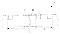
まず、図5に示すように、複数の個別半導体チップ11がウエハの上部面に形成されるため、ウエハ加工(fabrication)工程が行なわれ、少なくとも予備の電気的特性テスト(EDS test)が完了されたものである。チップ11の回路は保護層13により保護され、複数のチップパッド12はオープニング開口(openings)をより露出させる。ウエハには、図示のように、チップ11間ごとにS字状のスクライブレーンが形成される。
First, as shown in FIG. 5, since a plurality of
スクライブレーンに複数の穴15が形成される。チップ11と連結された穴15はスクライブレーン(S)の中間部にて分離される。実際の大きさは、ウエハ10の形態、チップ11の形態、使用された半導体製造工程の製造誤差によって異なるが、通常、ウエハに提供されるスクライブレーン(S)の幅は110〜220μm程度である。穴15は、レーザー切断装置や切断刃を用いた切断作業を行なう際、露出されずスクライブレーンの中間部において中心領域を約20〜40μm程度が除去されるように、大きさや位置がスクライブレーン(S)内に含まれることが望ましい。
A plurality of
穴15を形成する段階において、正確な位置、大きさ、並びに深さにより形成することができるドリルやエッチング工程が用いられる。直接ドリル技術、特に、レーザードリル技術がプラズマエッチング工程よりも単純であるため好まれる。その理由として、プラズマエッチング技術は、パターン用マスクの製作と製作されたパターン用マスクとをウエハ表面へ移送させる写真(photo)工程が追加的に必要で、製造工程が複雑で且つチップデザインを変更しなければならないという制約を伴う。一方、レーザードリルを用いる場合、パターン用マスクや写真工程の追加が不要で、さらにチップデザインを変更する必要がないため、既存のウエハ加工工程に全く影響を与えることなく、所望する位置、大きさ、及び深さの穴形成が可能である。
In the step of forming the
次に、図6に示すように、穴15内に伝導性物質、通常、金属を充填してスパッタリング、化学的気相蒸着方法、またはその他技術を用いて穴内壁に絶縁層16を形成する段階が行なわれて、接続穴15とウエハ10周辺物質との間の電気的接触が防止できる。絶縁膜16上に、スパッタリング、蒸発または電気メッキ技術を用いて障壁金属層17を形成する。障壁金属層17として、チタニウム、チタニウム窒化膜、チタニウム/タングステン、白金/シリコン、アルミニウム、並びにこれらの合金材から構成することができる。そして、障壁金属層17上にシード金属層18が形成される。その後、伝導性物質が蒸着或いは形成され、穴15を充填して接続ビア19が形成される。ここで、伝導性物質は、電気メッキ工程により穴15に蒸着され、銅、金、タングステン等の金属を形成する。
Next, as shown in FIG. 6, the
次に、図7では、接続ビア19とそれに対応するチップパッド12を連結させる段階を行なう。これは、再配線(redistribution)技術によって行なうことができる。すなわち、ウエハ表面に金属層を形成してチップパッド12とそれに対応する接続ビア19を接続し、公知の技術である、例えば、レジストリフトオフ(resist lift off)や金属エッチングを用いてパターニングして再配線21を形成する。再配線21は、接続ビア19と同時に形成することができる。再配線21形成の後に、カバー層23を形成して再配線21及び接続ビア19を外部環境から保護する。
Next, in FIG. 7, a step of connecting the connection via 19 and the
次に、図8に示すように、ウエハ背面(backside)において、所定厚さを除去する段階を行なう。この段階は、化学的機械研磨(CMP)やスピンウェットエッチング(spin wet etching)方法により行なうことができる。ウエハ10は、接続ビア19の下部を露出させるために所定の厚さを除去する。特に、スピンウェットエッチングの場合、機械的な損傷を起こさずウエハ10の厚さを50μm以下にまで薄膜化することができるので望ましい。
Next, as shown in FIG. 8, a step of removing a predetermined thickness is performed on the wafer backside. This step can be performed by chemical mechanical polishing (CMP) or spin wet etching. The
ウエハ10薄膜後、図9に示すように、絶縁物質を用いてウエハ10の背面に支持層25を形成して接続ビア19の下部面を開放する開口を形成する。支持層25は、ウエハ10の強度、またはハンドリング(handling)特性を向上させるとともに、薄厚のウエハの曲がりを防止できる。接着テープやポリイミド保護フィルムが一時的な支持層パターンとして用いられる場合、支持層パターン25は一時的なものとし得るか、永久的なものとし得る。
After the thin film of the
次に、図10に示すように、レーザー切断装置29を用いて薄型したウエハのスクライブレーン(S)の中心領域を切断してウエハ10を個別チップ単位に切断する段階を行なう。切断作業は、スクライブレーン(S)の周辺領域S1、S2に位置した接続ビア19が損傷されたり露出されないようにして行なわれる。そして、切断作業が完了すると、個別チップ11は、それぞれ外周に沿ってスクライブレーン(S)の周辺領域S1、S2に複数の接続ビア19を有することになる。切断過程において、支持層25は、レーザーにより切断されないよう、少なくとも一時的に個別チップ11を固定する。ウエハ10は、レーザー切断装置29を用いて個別チップ単位に切断できるが、ウエハにチッピング(chipping)、クラッキング(cracking)等の発生防止、並びにスクライブレーン(S)において除去された物質の幅の減少のために、レーザー切断装置29を用いたほうが望ましい。
Next, as shown in FIG. 10, a
次に、図11に示すように、チップスタックパッケージにおいて最下位チップ11aは、支持層25において除去されてテストウエハ30に実装される。テストウエハ30は、チップ11aに電気的、または機能的テストを適用する外部検査装置(図示せず)と電気的に接続する。図11に示すように、接続バンプ36を介して、チップ11aとテストウエハ30と、を物理的・電気的に接続しているが、図4に示すように、チップとテストウエハを互いに直接接続させることができる。接続バンプ36を用いる場合、接続バンプ36は、チップ11aの接続ビア19に対応する位置、例えば、ボールパッド又はボールランドに整列させる
Next, as shown in FIG. 11, the
一般に、熱圧着方法によって接続ビア19とテストウエハ30とを接合してリフロー、またはその他の方法によって接続ビア19とテストウエハとの接点を電気的・物理的に接続した後、外部検査装置(図示せず)によってチップ11aを検査して機能を評価するパッケージレベルテストが行なわれる。信頼性に問題のある半導体チップ11aは、ウエハ30において除去され、他のチップに取り替えてテストを進行することにより信頼性の検証が完了する。
Generally, the connection via 19 and the
そして、テストウエハに最下位に位置した半導体チップ11aの機能が検証されると、その上に上位半導体チップ11、すなわち、二番目層の半導体チップが積層される。二番目層の半導体チップ11を積層するために最下位のチップ11aの接続ビア19の上部に接続バンプ35が形成される。そして、二番目層の半導体チップ11の接続ビア19と最下位半導体チップ11aの接続ビア19とが熱的に接合される。
When the function of the
二番目層の半導体チップ11の実装が完了すると、二番目層の半導体チップ11に対するテストを行なう。信頼性に問題のある最下位半導体チップ11a及び二番目層チップ11は他のチップに取り替えられ、二番目層のチップの全てがテストを通過するとき迄、テストを行なう。図4に示すように、二番目層半導体チップ11及び上位半導体チップ11は接続バンプ無しに直接積層できる。
When the mounting of the second-
こうした基本的なチップ積層過程は、上位チップ11が積層されるごとに繰り返される。上位チップ11が積層される前、断層のチップが全てテストを通過することによってチップスタックパッケージに使用できるKGDのチップ積層となる。
Such a basic chip stacking process is repeated each time the
上述した通り、チップ積層過程において不良チップ11、11aは除去され、他のチップに取り替えられる。不良チップ11、11aを除去するために、不良チップを支持している接続バンプを溶かすに十分な量の熱を加える。それによって、隣接する、または下に位置する、チップの接続及び構造を変えることなく不良チップを除去できる。テストウエハより上に向かうほど益々低い溶融点を有する物質を接続バンプ35、36に用いれば、こうした結果を得ることができる。従って、下位層に実装されているKGDに影響を及ぼすことなく最上位に積層されたチップ11が除去できる。
As described above, the
そして、伝導性バンプ35、36の大きさは、接続ビア19の大きさに応じて決定することができ、一般に、約20〜60μm程度である。接続バンプ35、36は、公知の技術、ボールインジェクション(ball injection)方法やスクリーンプリンティング(screen printing)方法等により所望する大きさと位置に形成することができる。
The size of the
次に、図13に示すように、テストウエハ30の一部と半導体チップ11、11aを樹脂密封部41によりウエハレベルにて密封する段階を行なう。こうした密封段階は、ウエハレベルにて一度の作業でなされるため、工程進行においてチップレベルにおける密封の所要時間がより短くて済む。チップスタック構造の同じ平面上にあるチップの間隔に応じて樹脂密封部がチップスタック構造(図示せず)間の空間を完全に充填することもでき、或いは密封過程においてチップスタック構造を分離するためにモールドが用いられるためチップスタック構造間の空間をそのままにして置くこともできる。
Next, as shown in FIG. 13, a step of sealing a part of the
次に、図14に示すように、チップスタック11a、11間、またはテストウエハ30間の密封材41を切断することによって、単位スタックチップパッケージ100に切断する段階を行なう。密封完了後に、図3の共通基板31に対応するテストウエハ30の下部面に位置するビア33の下面にはんだボール45を貼り付ける過程を行なうことによって、PCBまたはその他基板にチップスタックパッケージが実装されて電気的に接続される。
Next, as shown in FIG. 14, a step of cutting the unit
一方、本明細書と図面には本発明の好適な実施形態について開示した。中には特定用語が使われたが、これは、単なる本発明の技術内容を容易に説明する上必要不可欠で、且つ、発明の理解を助けるための一般的な意味として使用したものであって、本発明の範囲を限定するものではない。ここに開示された実施例の他にも本発明の技術的思想に基づき他の変形例が実施可能であることは、本発明の属する技術分野における通常の知識を有する者であれば自明であろう。 On the other hand, the present specification and the drawings disclosed preferred embodiments of the present invention. Certain terms were used, but these were merely necessary to easily explain the technical content of the present invention, and were used as a general meaning to help understand the invention. It does not limit the scope of the present invention. It will be obvious to those skilled in the art to which the present invention pertains that other variations can be implemented based on the technical concept of the present invention in addition to the embodiments disclosed herein. Let's go.
10 ウエハ
11 半導体チップ
11a 半導体チップ
12 ボンディングパッド
13 保護膜
15 穴
16 絶縁膜
17 障壁金属層
18 シード金属層
19 貫通電極
21 再配線
23 保護膜
25 支持層
29 レーザー切断装置
30 テストウエハ
31 基板
33 ビア
35 ボールバンプ
36 ボールバンプ
41 樹脂密封部
45 はんだボール
100 スタックチップパッケージ
111 上チップ
119 接続ビア
131 共通基板
S スクライブレーン
S1、S2 周辺領域
DESCRIPTION OF
Claims (20)
背面と、チップ外周が形成されている活性面と、前記活性面のチップ外周より外側へ延びて形成されるスクライブレーンの一定部分と、前記スクライブレーンの一定部分内とを貫通して形成されて、上下面を有する複数の第1接続ビアとを備える第1チップと、
背面と、チップ外周が形成されている活性面と、前記活性面のチップ外周より外側へ延びて形成されているスクライブレーンの一定部分と、前記スクライブレーンの一定部分内とを貫通して形成されて、上下面を有する複数の第2接続ビアとを有する第2チップとを備えるチップスタックパッケージにおいて、
前記第1チップは、前記基板の第1面に位置して、前記第1接続ビアの下部面と前記基板端子とが電気的に接続されることにより前記第1チップと前記基板の第1面とが電気的に接続され、
前記第2チップは、前記第1チップの活性面に位置して、前記第2接続ビアの下部面と前記第1接続ビアの上部面とが電気的に接続することにより前記第2チップと前記第1チップの活性面とが電気的に接続されることを特徴とする、チップスタックパッケージ。 A substrate comprising a first surface having a plurality of substrate terminals and a second surface having a plurality of connection terminals in electrical contact with the substrate terminals;
A back surface, an active surface on which the outer periphery of the chip is formed, a fixed portion of a scribe lane formed extending outward from the outer periphery of the chip on the active surface, and a fixed portion of the scribe lane. A first chip comprising a plurality of first connection vias having upper and lower surfaces;
The back surface, the active surface on which the outer periphery of the chip is formed, the fixed portion of the scribe lane formed to extend outward from the outer periphery of the chip on the active surface, and the fixed portion of the scribe lane are formed. A chip stack package comprising a second chip having a plurality of second connection vias having upper and lower surfaces,
The first chip is located on the first surface of the substrate, and the lower surface of the first connection via and the substrate terminal are electrically connected, whereby the first chip and the first surface of the substrate are connected. And are electrically connected,
The second chip is located on the active surface of the first chip, and the lower surface of the second connection via and the upper surface of the first connection via are electrically connected to each other, whereby the second chip and the second chip are electrically connected. A chip stack package, wherein the active surface of the first chip is electrically connected.
各チップの外周と隣接のスクライブレーンの周辺部に複数の穴を形成する段階と、
前記穴に金属を充填して接続ビアを形成する段階と、
前記チップパッドとそれに対応する接続ビアを電気的に接続する段階と、
前記接続ビアの下部面を露出させて前記ウエハの背面から一定厚さを除去して薄型のウエハを形成する段階と、
前記スクライブレーンの周辺部はそのままにしながら中心領域を除去して前記薄型のウエハを個別チップに分離する段階と、
複数の個別チップをテストウエハに実装させて接続ビアがそれに対応する基板端子と電気的に接続する段階と、
前記テストウエハの接点を介して複数の第1個別チップに対する第1ウエハレベルテストをする段階と、
複数の第2個別チップを前記複数の第1個別チップに積層して複数のチップスタック構造を形成することにより前記第2個別チップの接続ビア及び前記第1個熱チップの接続ビアを電気的に接続する段階と、
前記テストウエハの接点を介して前記第2個別チップに対する第1ウエハレベルテスト及び第2ウエハレベルテストする段階と、
前記複数のチップスタック構造を密封する段階と、
前記複数のチップスタック構造を分離して単位チップスタックパッケージに形成する段階と、を有することを特徴とする、チップスタックパッケージ製造方法。 A plurality of chips each having an integrated circuit and a chip pad formed on the front surface, wherein the chip pads are arranged in the outer periphery of the chip and a scribe lane is formed between the chips; Providing the above wafers;
Forming a plurality of holes in the periphery of each chip and in the periphery of the adjacent scribe lane;
Filling the holes with metal to form connection vias;
Electrically connecting the chip pad and the corresponding connection via;
Exposing a lower surface of the connection via to remove a certain thickness from the back surface of the wafer to form a thin wafer;
Removing the central region while leaving the periphery of the scribe lane as it is, and separating the thin wafer into individual chips;
Mounting a plurality of individual chips on a test wafer and electrically connecting connection vias to corresponding substrate terminals;
Performing a first wafer level test on a plurality of first individual chips via the contact of the test wafer;
A plurality of second individual chips are stacked on the plurality of first individual chips to form a plurality of chip stack structures, thereby electrically connecting the connection vias of the second individual chip and the connection vias of the first thermal chip. Connecting, and
Performing a first wafer level test and a second wafer level test on the second individual chip via the contact of the test wafer;
Sealing the plurality of chip stack structures;
Separating the plurality of chip stack structures into unit chip stack packages, and manufacturing the chip stack packages.
前記複数の第2チップを積層する段階は、第2接続バンプを前記複数の第1チップを備える段階と、前記第2接続バンプを熱的に処理してそれに対応する第1接続ビアと接合させる段階とを有することを特徴とする、請求項13に記載のチップスタックパッケージ製造方法。 The step of mounting the plurality of first chips includes a step of providing a first connection bump on the test wafer, and a step of thermally processing the first connection bump and bonding it to a corresponding substrate terminal. ,
The step of laminating the plurality of second chips includes the step of providing second connection bumps with the plurality of first chips, and thermally processing the second connection bumps to join the corresponding first connection vias. The method of manufacturing a chip stack package according to claim 13, further comprising:
前記除去された個別チップを代替個別チップに取り替えて複数の第1個別チップを改善する段階と、
少なくともそれぞれの代替個別チップに対して第1ウエハレベルテストをする段階と、
前記複数の第2個別チップを積層する前に、前記複数の第1個別チップが良質のチップだけを有するようになる迄、前記除去、取り替え、第1ウエハレベルテストの実行段階を繰り返す段階と、
前記第1ウエハレベルテスト及び第2ウエハレベルテストにおいて不良と判定された前記複数の第2個別チップを除去する段階と、
前記除去された個別チップを代替個別チップに取り替えて複数の第2個別チップを改善する段階と、
少なくともそれぞれの代替個別チップに対して第1ウエハレベルテスト及び第2ウエハレベルテストする段階と、
前記複数のチップスタック構造を密封する前に、前記複数の第2個別チップが良質のチップだけを有するようになる迄、前記除去、交替、第1ウエハレベルテスト及び第2ウエハレベルテストの実行段階を繰り返す段階と、を有することを特徴とするチップスタックパッケージ製造方法。 Removing the first individual chip determined to be defective in the first wafer level test;
Replacing the removed individual chips with alternative individual chips to improve a plurality of first individual chips;
Performing a first wafer level test on at least each alternate individual chip;
Repeating the steps of removing, replacing, and performing the first wafer level test until the plurality of first individual chips have only good quality chips before stacking the plurality of second individual chips;
Removing the plurality of second individual chips determined to be defective in the first wafer level test and the second wafer level test;
Replacing the removed individual chips with alternative individual chips to improve a plurality of second individual chips;
Performing a first wafer level test and a second wafer level test on at least each alternative individual chip;
Performing the removal, replacement, first wafer level test, and second wafer level test until the plurality of second individual chips have only good quality chips before sealing the plurality of chip stack structures; A method of manufacturing a chip stack package, comprising:
各チップの外周と隣接するスクライブレーンの周辺部に複数の穴を形成する段階と、
前記穴に金属を詰め込んで接続ビアを形成する段階と、
前記チップパッドとそれに対応する接続ビアを電気的に接続する段階と、
前記接続ビアの下部面を露出するために前記ウエハの背面において一定厚さを除去して薄型のウエハを形成する段階と、
前記スクライブレーンの周辺部はそのままにしながら中心領域を除去して前記薄型のウエハをN個の個別チップに分離する段階と、
第1ウエハから得られたM個から成る複数の第1個別チップをテストウエハに実装させて接続ビアがそれに対応する基板端子と電気的に接続する段階と、
前記テストウエハの接点を介して複数の第1個別チップに対する第1ウエハレベルテストする段階と、
第2ウエハから得られたM個から成る複数の第2個別チップを前記複数の第1個別チップに積層して複数のMチップスタック構造を形成することにより前記第2個別チップの接続ビアと前記第1個別チップの接続ビアとを電気的に接続する段階と、
前記テストウエハの接点を介して前記第2個別チップに対する第1及び第2ウエハレベルテストをする段階と、
前記複数のチップスタック構造を密封する段階と、
前記複数のチップスタック構造を支持するテストウエハの個別部分を分離して基板として用いられるM個の単位チップスタックパッケージに形成する段階と、を有することを特徴とする、請求項1に記載のチップスタックパッケージ製造方法。 A plurality of wafers having a front surface and a back surface, wherein N chips each including an integrated circuit and a chip pad are formed on the front surface, the chip pads are arranged in the outer periphery of the chip, and a scribe lane is formed between the chips. Comprising the steps of:
Forming a plurality of holes in the periphery of the scribe lane adjacent to the outer periphery of each chip;
Filling the holes with metal to form connection vias;
Electrically connecting the chip pad and the corresponding connection via;
Removing a constant thickness on the back surface of the wafer to expose a lower surface of the connection via to form a thin wafer;
Removing the central region while leaving the periphery of the scribe lane as it is, and separating the thin wafer into N individual chips;
Mounting a plurality of M individual chips obtained from the first wafer on the test wafer and electrically connecting the connection vias to the corresponding substrate terminals;
Performing a first wafer level test on a plurality of first individual chips via the contact of the test wafer;
A plurality of M second individual chips obtained from the second wafer are stacked on the plurality of first individual chips to form a plurality of M chip stack structures, thereby connecting the connection vias of the second individual chips and the second individual chips. Electrically connecting the connection vias of the first individual chip;
Performing first and second wafer level tests on the second individual chips via the contact of the test wafer;
Sealing the plurality of chip stack structures;
2. The chip according to claim 1, further comprising: separating individual parts of the test wafer supporting the plurality of chip stack structures into M unit chip stack packages used as substrates. 3. Stack package manufacturing method.
前記不良チップを新しい個別チップに取り替えて複数の第1個別チップを改善する段階と、
前記新しい個別チップをテストする段階と、
前記複数の第2個別チップを積層する前に、前記第1個別チップが全てKGBになる迄、前記確認、取り替え、テスト段階を繰り返す段階と、
を有することを特徴とする、請求項18に記載のチップスタックパッケージ製造方法。 Performing a first wafer level test on the plurality of first individual chips; checking a defective chip;
Replacing the defective chip with a new individual chip to improve a plurality of first individual chips;
Testing the new individual chip;
Repeating the checking, replacing, and testing steps until the first individual chips are all KGB before stacking the plurality of second individual chips;
The chip stack package manufacturing method according to claim 18, comprising:
Applications Claiming Priority (1)
| Application Number | Priority Date | Filing Date | Title |
|---|---|---|---|
| KR10-2003-0059166A KR100537892B1 (en) | 2003-08-26 | 2003-08-26 | Chip stack package and manufacturing method thereof |
Publications (2)
| Publication Number | Publication Date |
|---|---|
| JP2005072596A true JP2005072596A (en) | 2005-03-17 |
| JP4602715B2 JP4602715B2 (en) | 2010-12-22 |
Family
ID=34214705
Family Applications (1)
| Application Number | Title | Priority Date | Filing Date |
|---|---|---|---|
| JP2004242970A Expired - Fee Related JP4602715B2 (en) | 2003-08-26 | 2004-08-23 | Chip stack package and manufacturing method thereof |
Country Status (3)
| Country | Link |
|---|---|
| US (4) | US7276799B2 (en) |
| JP (1) | JP4602715B2 (en) |
| KR (1) | KR100537892B1 (en) |
Cited By (18)
| Publication number | Priority date | Publication date | Assignee | Title |
|---|---|---|---|---|
| JP2006278552A (en) * | 2005-03-28 | 2006-10-12 | Fujitsu Ltd | Semiconductor device and manufacturing method of semiconductor device |
| JP2006278817A (en) * | 2005-03-30 | 2006-10-12 | Oki Electric Ind Co Ltd | LAMINATED STRUCTURE FORMATION METHOD AND SEMICONDUCTOR DEVICE MANUFACTURING METHOD USING THE METHOD |
| JP2007036184A (en) * | 2005-06-24 | 2007-02-08 | Seiko Epson Corp | SEMICONDUCTOR DEVICE, ITS MANUFACTURING METHOD, AND ELECTRONIC DEVICE |
| US7288841B2 (en) | 2005-06-13 | 2007-10-30 | Shinko Electric Industries, Co., Ltd. | Laminated semiconductor package |
| JP2008227348A (en) * | 2007-03-15 | 2008-09-25 | Sanyo Electric Co Ltd | Semiconductor device and manufacturing method thereof |
| JP2008306105A (en) * | 2007-06-11 | 2008-12-18 | Oki Electric Ind Co Ltd | Manufacturing method of semiconductor device |
| JP2009004722A (en) * | 2007-06-20 | 2009-01-08 | Hynix Semiconductor Inc | Manufacturing method of semiconductor package |
| US7491582B2 (en) | 2004-08-31 | 2009-02-17 | Seiko Epson Corporation | Method for manufacturing semiconductor device and semiconductor device |
| US7595559B2 (en) | 2004-07-27 | 2009-09-29 | Samsung Electronics Co., Ltd. | Integrated circuit chip having pass-through vias therein that extend between multiple integrated circuits on the chip |
| JP2010016377A (en) * | 2008-06-30 | 2010-01-21 | Intel Corp | Multiple-die integrated circuit device and method |
| JP2010507254A (en) * | 2006-10-19 | 2010-03-04 | マイクロン テクノロジー, インク. | Method for manufacturing layered chip package |
| JP2010245536A (en) * | 2009-04-03 | 2010-10-28 | Samsung Electronics Co Ltd | Semiconductor device and manufacturing method thereof |
| JP2011159869A (en) * | 2010-02-02 | 2011-08-18 | Nec Corp | Laminate structure of semiconductor device and method for manufacturing the same |
| US8141243B2 (en) | 2007-03-08 | 2012-03-27 | Sony Corporation | Method of manufacturing circuit board |
| JP2014003272A (en) * | 2012-05-24 | 2014-01-09 | Napura:Kk | Multilayer substrate |
| JP2014078768A (en) * | 2006-08-08 | 2014-05-01 | Samsung Electronics Co Ltd | Semiconductor device where multiple semiconductor chips of different sizes are laminated, and multi-chip package comprising the same |
| US8729691B2 (en) | 2006-08-31 | 2014-05-20 | Micron Technology, Inc. | Distributed semiconductor device methods, apparatus, and systems |
| US9006586B2 (en) | 2011-06-27 | 2015-04-14 | Shinko Electric Industries Co., Ltd. | Wiring substrate, its manufacturing method, and semiconductor device |
Families Citing this family (440)
| Publication number | Priority date | Publication date | Assignee | Title |
|---|---|---|---|---|
| US6930256B1 (en) | 2002-05-01 | 2005-08-16 | Amkor Technology, Inc. | Integrated circuit substrate having laser-embedded conductive patterns and method therefor |
| US7548430B1 (en) | 2002-05-01 | 2009-06-16 | Amkor Technology, Inc. | Buildup dielectric and metallization process and semiconductor package |
| US9691635B1 (en) | 2002-05-01 | 2017-06-27 | Amkor Technology, Inc. | Buildup dielectric layer having metallization pattern semiconductor package fabrication method |
| US7633765B1 (en) | 2004-03-23 | 2009-12-15 | Amkor Technology, Inc. | Semiconductor package including a top-surface metal layer for implementing circuit features |
| JP2005051150A (en) * | 2003-07-31 | 2005-02-24 | Seiko Epson Corp | Semiconductor device and manufacturing method thereof, circuit board, and electronic apparatus |
| KR100537892B1 (en) * | 2003-08-26 | 2005-12-21 | 삼성전자주식회사 | Chip stack package and manufacturing method thereof |
| JP4340517B2 (en) * | 2003-10-30 | 2009-10-07 | Okiセミコンダクタ株式会社 | Semiconductor device and manufacturing method thereof |
| US8084866B2 (en) | 2003-12-10 | 2011-12-27 | Micron Technology, Inc. | Microelectronic devices and methods for filling vias in microelectronic devices |
| US7091124B2 (en) * | 2003-11-13 | 2006-08-15 | Micron Technology, Inc. | Methods for forming vias in microelectronic devices, and methods for packaging microelectronic devices |
| US11081370B2 (en) | 2004-03-23 | 2021-08-03 | Amkor Technology Singapore Holding Pte. Ltd. | Methods of manufacturing an encapsulated semiconductor device |
| US10811277B2 (en) | 2004-03-23 | 2020-10-20 | Amkor Technology, Inc. | Encapsulated semiconductor package |
| US20050247894A1 (en) * | 2004-05-05 | 2005-11-10 | Watkins Charles M | Systems and methods for forming apertures in microfeature workpieces |
| US7232754B2 (en) | 2004-06-29 | 2007-06-19 | Micron Technology, Inc. | Microelectronic devices and methods for forming interconnects in microelectronic devices |
| US20060019468A1 (en) * | 2004-07-21 | 2006-01-26 | Beatty John J | Method of manufacturing a plurality of electronic assemblies |
| US7425499B2 (en) * | 2004-08-24 | 2008-09-16 | Micron Technology, Inc. | Methods for forming interconnects in vias and microelectronic workpieces including such interconnects |
| SG120200A1 (en) | 2004-08-27 | 2006-03-28 | Micron Technology Inc | Slanted vias for electrical circuits on circuit boards and other substrates |
| US7419852B2 (en) * | 2004-08-27 | 2008-09-02 | Micron Technology, Inc. | Low temperature methods of forming back side redistribution layers in association with through wafer interconnects, semiconductor devices including same, and assemblies |
| US7300857B2 (en) | 2004-09-02 | 2007-11-27 | Micron Technology, Inc. | Through-wafer interconnects for photoimager and memory wafers |
| US7271482B2 (en) | 2004-12-30 | 2007-09-18 | Micron Technology, Inc. | Methods for forming interconnects in microelectronic workpieces and microelectronic workpieces formed using such methods |
| US8093694B2 (en) * | 2005-02-14 | 2012-01-10 | Stats Chippac Ltd. | Method of manufacturing non-leaded integrated circuit package system having etched differential height lead structures |
| US7714451B2 (en) * | 2005-02-18 | 2010-05-11 | Stats Chippac Ltd. | Semiconductor package system with thermal die bonding |
| JP4551255B2 (en) * | 2005-03-31 | 2010-09-22 | ルネサスエレクトロニクス株式会社 | Semiconductor device |
| KR100609334B1 (en) * | 2005-06-13 | 2006-08-08 | 삼성전자주식회사 | Laminated circuit member having a photosensitive polymer gap-filled and a method of manufacturing the same |
| US7589406B2 (en) * | 2005-06-27 | 2009-09-15 | Micron Technology, Inc. | Stacked semiconductor component |
| US7795134B2 (en) | 2005-06-28 | 2010-09-14 | Micron Technology, Inc. | Conductive interconnect structures and formation methods using supercritical fluids |
| JP4507101B2 (en) | 2005-06-30 | 2010-07-21 | エルピーダメモリ株式会社 | Semiconductor memory device and manufacturing method thereof |
| TWI292178B (en) * | 2005-07-01 | 2008-01-01 | Yu Nung Shen | Stacked semiconductor chip package |
| TW200717680A (en) * | 2005-07-19 | 2007-05-01 | Koninkl Philips Electronics Nv | Method of manufacturing a system in package |
| US7863187B2 (en) | 2005-09-01 | 2011-01-04 | Micron Technology, Inc. | Microfeature workpieces and methods for forming interconnects in microfeature workpieces |
| US7622377B2 (en) | 2005-09-01 | 2009-11-24 | Micron Technology, Inc. | Microfeature workpiece substrates having through-substrate vias, and associated methods of formation |
| US7262134B2 (en) | 2005-09-01 | 2007-08-28 | Micron Technology, Inc. | Microfeature workpieces and methods for forming interconnects in microfeature workpieces |
| US7358616B2 (en) * | 2005-09-14 | 2008-04-15 | Freescale Semiconductor, Inc. | Semiconductor stacked die/wafer configuration and packaging and method thereof |
| KR100713121B1 (en) | 2005-09-27 | 2007-05-02 | 한국전자통신연구원 | Chips and Chip Stacks Using the Same |
| JP4395775B2 (en) * | 2005-10-05 | 2010-01-13 | ソニー株式会社 | Semiconductor device and manufacturing method thereof |
| US8810031B2 (en) * | 2005-10-26 | 2014-08-19 | Industrial Technology Research Institute | Wafer-to-wafer stack with supporting pedestal |
| TWI285419B (en) | 2005-10-26 | 2007-08-11 | Ind Tech Res Inst | Wafer-to-wafer stacking with supporting pedestals |
| EP1949432B1 (en) * | 2005-11-08 | 2017-10-18 | Invensas Corporation | Producing a covered through substrate via using a temporary cap layer |
| JP4390775B2 (en) * | 2006-02-08 | 2009-12-24 | Okiセミコンダクタ株式会社 | Manufacturing method of semiconductor package |
| KR100694424B1 (en) * | 2006-02-17 | 2007-03-12 | 주식회사 하이닉스반도체 | Multi chip package device and method for manufacturing the same |
| JP2007242853A (en) * | 2006-03-08 | 2007-09-20 | Sanken Electric Co Ltd | Semiconductor substrate and semiconductor device using the same |
| KR100753415B1 (en) * | 2006-03-17 | 2007-08-30 | 주식회사 하이닉스반도체 | Stack package |
| KR100884238B1 (en) * | 2006-05-22 | 2009-02-17 | 삼성전자주식회사 | Semiconductor package having anchor type coupling structure and manufacturing method thereof |
| KR100837269B1 (en) * | 2006-05-22 | 2008-06-11 | 삼성전자주식회사 | Wafer level package and manufacturing method thereof |
| US7749899B2 (en) | 2006-06-01 | 2010-07-06 | Micron Technology, Inc. | Microelectronic workpieces and methods and systems for forming interconnects in microelectronic workpieces |
| JP4237207B2 (en) * | 2006-07-07 | 2009-03-11 | エルピーダメモリ株式会社 | Manufacturing method of semiconductor device |
| KR100794658B1 (en) * | 2006-07-07 | 2008-01-14 | 삼성전자주식회사 | Method of manufacturing semiconductor chip, semiconductor chip formed thereby and chip stack package comprising same |
| KR100735483B1 (en) * | 2006-08-23 | 2007-07-03 | 동부일렉트로닉스 주식회사 | Semiconductor device and manufacturing method |
| US7629249B2 (en) | 2006-08-28 | 2009-12-08 | Micron Technology, Inc. | Microfeature workpieces having conductive interconnect structures formed by chemically reactive processes, and associated systems and methods |
| US8021981B2 (en) | 2006-08-30 | 2011-09-20 | Micron Technology, Inc. | Redistribution layers for microfeature workpieces, and associated systems and methods |
| US7902643B2 (en) | 2006-08-31 | 2011-03-08 | Micron Technology, Inc. | Microfeature workpieces having interconnects and conductive backplanes, and associated systems and methods |
| KR100832845B1 (en) * | 2006-10-03 | 2008-05-28 | 삼성전자주식회사 | Semiconductor package structure and manufacturing method thereof |
| US7829438B2 (en) | 2006-10-10 | 2010-11-09 | Tessera, Inc. | Edge connect wafer level stacking |
| US8513789B2 (en) | 2006-10-10 | 2013-08-20 | Tessera, Inc. | Edge connect wafer level stacking with leads extending along edges |
| US7901989B2 (en) | 2006-10-10 | 2011-03-08 | Tessera, Inc. | Reconstituted wafer level stacking |
| US7759166B2 (en) * | 2006-10-17 | 2010-07-20 | Tessera, Inc. | Microelectronic packages fabricated at the wafer level and methods therefor |
| JP4312786B2 (en) * | 2006-11-02 | 2009-08-12 | Okiセミコンダクタ株式会社 | Manufacturing method of semiconductor chip |
| US7550857B1 (en) * | 2006-11-16 | 2009-06-23 | Amkor Technology, Inc. | Stacked redistribution layer (RDL) die assembly package |
| US8569876B2 (en) * | 2006-11-22 | 2013-10-29 | Tessera, Inc. | Packaged semiconductor chips with array |
| US7791199B2 (en) * | 2006-11-22 | 2010-09-07 | Tessera, Inc. | Packaged semiconductor chips |
| KR100800486B1 (en) * | 2006-11-24 | 2008-02-04 | 삼성전자주식회사 | Semiconductor memory device having improved signal transmission path and driving method thereof |
| KR100843213B1 (en) * | 2006-12-05 | 2008-07-02 | 삼성전자주식회사 | Multiple input-output semiconductor chip package and method for manufacturing the memory chip and the processor chip connected through a through electrode arranged in the scribe region |
| US8124429B2 (en) * | 2006-12-15 | 2012-02-28 | Richard Norman | Reprogrammable circuit board with alignment-insensitive support for multiple component contact types |
| KR100833194B1 (en) * | 2006-12-19 | 2008-05-28 | 삼성전자주식회사 | Semiconductor package and manufacturing method in which wiring layer of semiconductor chip is directly connected to substrate |
| US20080157322A1 (en) * | 2006-12-27 | 2008-07-03 | Jia Miao Tang | Double side stacked die package |
| US7952195B2 (en) | 2006-12-28 | 2011-05-31 | Tessera, Inc. | Stacked packages with bridging traces |
| US8035207B2 (en) * | 2006-12-30 | 2011-10-11 | Stats Chippac Ltd. | Stackable integrated circuit package system with recess |
| KR100827667B1 (en) * | 2007-01-16 | 2008-05-07 | 삼성전자주식회사 | A semiconductor package having a semiconductor chip in a substrate and a method of manufacturing the same |
| US7618857B2 (en) * | 2007-01-17 | 2009-11-17 | International Business Machines Corporation | Method of reducing detrimental STI-induced stress in MOSFET channels |
| KR101030769B1 (en) * | 2007-01-23 | 2011-04-27 | 삼성전자주식회사 | Stack Packages and Stack Packaging Methods |
| KR100875955B1 (en) * | 2007-01-25 | 2008-12-26 | 삼성전자주식회사 | Stacked package and its manufacturing method |
| EP2135280A2 (en) | 2007-03-05 | 2009-12-23 | Tessera, Inc. | Chips having rear contacts connected by through vias to front contacts |
| KR100842916B1 (en) * | 2007-03-09 | 2008-07-03 | 주식회사 하이닉스반도체 | Manufacturing method of stack package |
| KR100845006B1 (en) * | 2007-03-19 | 2008-07-09 | 삼성전자주식회사 | Laminated chip package and its manufacturing method |
| KR100843240B1 (en) * | 2007-03-23 | 2008-07-03 | 삼성전자주식회사 | A method of forming a through electrode of a semiconductor device for a wafer level stack and a semiconductor device for a wafer level stack |
| KR100871709B1 (en) | 2007-04-10 | 2008-12-08 | 삼성전자주식회사 | Chip stack package and manufacturing method thereof |
| US8445325B2 (en) * | 2007-05-04 | 2013-05-21 | Stats Chippac, Ltd. | Package-in-package using through-hole via die on saw streets |
| US7569421B2 (en) * | 2007-05-04 | 2009-08-04 | Stats Chippac, Ltd. | Through-hole via on saw streets |
| US8232183B2 (en) * | 2007-05-04 | 2012-07-31 | Taiwan Semiconductor Manufacturing Company, Ltd. | Process and apparatus for wafer-level flip-chip assembly |
| US7723159B2 (en) * | 2007-05-04 | 2010-05-25 | Stats Chippac, Ltd. | Package-on-package using through-hole via die on saw streets |
| US7829998B2 (en) | 2007-05-04 | 2010-11-09 | Stats Chippac, Ltd. | Semiconductor wafer having through-hole vias on saw streets with backside redistribution layer |
| KR100866966B1 (en) * | 2007-05-10 | 2008-11-06 | 삼성전자주식회사 | Nonvolatile Memory Devices, Manufacturing Methods And Semiconductor Packages |
| US20080284037A1 (en) * | 2007-05-15 | 2008-11-20 | Andry Paul S | Apparatus and Methods for Constructing Semiconductor Chip Packages with Silicon Space Transformer Carriers |
| US7883938B2 (en) * | 2007-05-22 | 2011-02-08 | United Test And Assembly Center Ltd. | Stacked die semiconductor package and method of assembly |
| US8367471B2 (en) | 2007-06-15 | 2013-02-05 | Micron Technology, Inc. | Semiconductor assemblies, stacked semiconductor devices, and methods of manufacturing semiconductor assemblies and stacked semiconductor devices |
| KR100914977B1 (en) | 2007-06-18 | 2009-09-02 | 주식회사 하이닉스반도체 | Method for fabricating stack package |
| KR100945504B1 (en) * | 2007-06-26 | 2010-03-09 | 주식회사 하이닉스반도체 | Stacked package and its manufacturing method |
| KR100876890B1 (en) * | 2007-06-26 | 2009-01-07 | 주식회사 하이닉스반도체 | Semiconductor package and manufacturing method thereof |
| SG149710A1 (en) * | 2007-07-12 | 2009-02-27 | Micron Technology Inc | Interconnects for packaged semiconductor devices and methods for manufacturing such devices |
| KR100906065B1 (en) * | 2007-07-12 | 2009-07-03 | 주식회사 동부하이텍 | Semiconductor chip, manufacturing method thereof and laminated package having same |
| US7825517B2 (en) * | 2007-07-16 | 2010-11-02 | Taiwan Semiconductor Manufacturing Company, Ltd. | Method for packaging semiconductor dies having through-silicon vias |
| US7969023B2 (en) * | 2007-07-16 | 2011-06-28 | Stats Chippac Ltd. | Integrated circuit package system with triple film spacer having embedded fillers and method of manufacture thereof |
| CN101809739B (en) | 2007-07-27 | 2014-08-20 | 泰塞拉公司 | Reconstituted wafer stack packaging with after-applied pad extensions |
| EP2183770B1 (en) * | 2007-07-31 | 2020-05-13 | Invensas Corporation | Method of forming through-substrate vias and corresponding decvice |
| CN101861646B (en) | 2007-08-03 | 2015-03-18 | 泰塞拉公司 | Stacked packages utilizing reconstituted wafers |
| US7781877B2 (en) | 2007-08-07 | 2010-08-24 | Micron Technology, Inc. | Packaged integrated circuit devices with through-body conductive vias, and methods of making same |
| US8043895B2 (en) | 2007-08-09 | 2011-10-25 | Tessera, Inc. | Method of fabricating stacked assembly including plurality of stacked microelectronic elements |
| KR100905784B1 (en) * | 2007-08-16 | 2009-07-02 | 주식회사 하이닉스반도체 | Through-electrode for semiconductor package and semiconductor package having same |
| KR101348748B1 (en) * | 2007-08-24 | 2014-01-08 | 삼성전자주식회사 | Method for manufacturing a semiconductor package using a pad redistribution substrate |
| JP5114130B2 (en) * | 2007-08-24 | 2013-01-09 | 新光電気工業株式会社 | WIRING BOARD, MANUFACTURING METHOD THEREOF, AND SEMICONDUCTOR DEVICE |
| SG150410A1 (en) | 2007-08-31 | 2009-03-30 | Micron Technology Inc | Partitioned through-layer via and associated systems and methods |
| US7838978B2 (en) * | 2007-09-19 | 2010-11-23 | Infineon Technologies Ag | Semiconductor device |
| US8415783B1 (en) * | 2007-10-04 | 2013-04-09 | Xilinx, Inc. | Apparatus and methodology for testing stacked die |
| KR100886720B1 (en) * | 2007-10-30 | 2009-03-04 | 주식회사 하이닉스반도체 | Laminated semiconductor package and method for manufacturing same |
| US8294149B2 (en) | 2007-11-06 | 2012-10-23 | International Business Machines Corporation | Test structure and methodology for three-dimensional semiconductor structures |
| KR101374338B1 (en) * | 2007-11-14 | 2014-03-14 | 삼성전자주식회사 | semicondoctor device having through-via and method of forming the same |
| US8492263B2 (en) | 2007-11-16 | 2013-07-23 | Taiwan Semiconductor Manufacturing Company, Ltd. | Protected solder ball joints in wafer level chip-scale packaging |
| KR100919860B1 (en) * | 2007-11-26 | 2009-09-30 | 파워테크 테크놀로지 인코포레이티드 | Semiconductor Chip Device Having Through-Silicon-Via (TSV) and Its Fabrication Method |
| US7790576B2 (en) * | 2007-11-29 | 2010-09-07 | Stats Chippac, Ltd. | Semiconductor device and method of forming through hole vias in die extension region around periphery of die |
| US20090140408A1 (en) * | 2007-11-30 | 2009-06-04 | Taewoo Lee | Integrated circuit package-on-package system with stacking via interconnect |
| US7884015B2 (en) | 2007-12-06 | 2011-02-08 | Micron Technology, Inc. | Methods for forming interconnects in microelectronic workpieces and microelectronic workpieces formed using such methods |
| US8399973B2 (en) * | 2007-12-20 | 2013-03-19 | Mosaid Technologies Incorporated | Data storage and stackable configurations |
| US7791175B2 (en) * | 2007-12-20 | 2010-09-07 | Mosaid Technologies Incorporated | Method for stacking serially-connected integrated circuits and multi-chip device made from same |
| EP2075832B1 (en) * | 2007-12-27 | 2010-09-15 | Imec | Method for aligning and bonding elements and a device comprising aligned and bonded elements |
| US8084854B2 (en) | 2007-12-28 | 2011-12-27 | Micron Technology, Inc. | Pass-through 3D interconnect for microelectronic dies and associated systems and methods |
| US7956453B1 (en) * | 2008-01-16 | 2011-06-07 | Amkor Technology, Inc. | Semiconductor package with patterning layer and method of making same |
| US20090184414A1 (en) * | 2008-01-22 | 2009-07-23 | Chang Jun Park | Wafer level chip scale package having an enhanced heat exchange efficiency with an emf shield and a method for fabricating the same |
| US7948095B2 (en) * | 2008-02-12 | 2011-05-24 | United Test And Assembly Center Ltd. | Semiconductor package and method of making the same |
| US20090212381A1 (en) * | 2008-02-26 | 2009-08-27 | Tessera, Inc. | Wafer level packages for rear-face illuminated solid state image sensors |
| US20100053407A1 (en) * | 2008-02-26 | 2010-03-04 | Tessera, Inc. | Wafer level compliant packages for rear-face illuminated solid state image sensors |
| TWI352412B (en) * | 2008-03-03 | 2011-11-11 | Advanced Semiconductor Eng | Multi-chip package structure and method of fabrica |
| KR100959603B1 (en) * | 2008-03-07 | 2010-05-27 | 주식회사 하이닉스반도체 | Method of manufacturing wafer level package |
| US8072079B2 (en) * | 2008-03-27 | 2011-12-06 | Stats Chippac, Ltd. | Through hole vias at saw streets including protrusions or recesses for interconnection |
| SG142321A1 (en) | 2008-04-24 | 2009-11-26 | Micron Technology Inc | Pre-encapsulated cavity interposer |
| US7973416B2 (en) * | 2008-05-12 | 2011-07-05 | Texas Instruments Incorporated | Thru silicon enabled die stacking scheme |
| US7960840B2 (en) * | 2008-05-12 | 2011-06-14 | Texas Instruments Incorporated | Double wafer carrier process for creating integrated circuit die with through-silicon vias and micro-electro-mechanical systems protected by a hermetic cavity created at the wafer level |
| TWI389291B (en) * | 2008-05-13 | 2013-03-11 | 財團法人工業技術研究院 | Three-dimensional stacked die package structure |
| US8253230B2 (en) | 2008-05-15 | 2012-08-28 | Micron Technology, Inc. | Disabling electrical connections using pass-through 3D interconnects and associated systems and methods |
| TWI443790B (en) * | 2008-05-21 | 2014-07-01 | 精材科技股份有限公司 | Electronics device package and method for fabricating thereof |
| US7648911B2 (en) * | 2008-05-27 | 2010-01-19 | Stats Chippac, Ltd. | Semiconductor device and method of forming embedded passive circuit elements interconnected to through hole vias |
| KR101040533B1 (en) * | 2008-05-28 | 2011-06-16 | 한국과학기술원 | Semiconductor device and manufacturing method |
| KR101458958B1 (en) * | 2008-06-10 | 2014-11-13 | 삼성전자주식회사 | Semiconductor chip, semiconductor package, and method of fabricating the semiconductor chip |
| KR101655897B1 (en) | 2008-06-16 | 2016-09-08 | 테세라, 인코포레이티드 | A microelectronic assembly and a method of fabricating a stacked microelectronic assembly |
| US8334170B2 (en) | 2008-06-27 | 2012-12-18 | Taiwan Semiconductor Manufacturing Company, Ltd. | Method for stacking devices |
| KR101020876B1 (en) | 2008-07-07 | 2011-03-09 | 박태석 | Wafer Level Chip Scale Package and Fabrication Method of Semiconductor Device by Through Hole Interconnect |
| US7659145B2 (en) * | 2008-07-14 | 2010-02-09 | Stats Chippac, Ltd. | Semiconductor device and method of forming stepped-down RDL and recessed THV in peripheral region of the device |
| SG10201505279RA (en) * | 2008-07-18 | 2015-10-29 | Utac Headquarters Pte Ltd | Packaging structural member |
| US7851346B2 (en) * | 2008-07-21 | 2010-12-14 | Taiwan Semiconductor Manufacturing Company, Ltd. | Bonding metallurgy for three-dimensional interconnect |
| US7843072B1 (en) * | 2008-08-12 | 2010-11-30 | Amkor Technology, Inc. | Semiconductor package having through holes |
| US8932906B2 (en) | 2008-08-19 | 2015-01-13 | Taiwan Semiconductor Manufacturing Company, Ltd. | Through silicon via bonding structure |
| US8334599B2 (en) * | 2008-08-21 | 2012-12-18 | Qimonda Ag | Electronic device having a chip stack |
| KR100992450B1 (en) * | 2008-08-21 | 2010-11-08 | 엘지이노텍 주식회사 | Multilayer chip package |
| US9524945B2 (en) | 2010-05-18 | 2016-12-20 | Taiwan Semiconductor Manufacturing Company, Ltd. | Cu pillar bump with L-shaped non-metal sidewall protection structure |
| US8030780B2 (en) | 2008-10-16 | 2011-10-04 | Micron Technology, Inc. | Semiconductor substrates with unitary vias and via terminals, and associated systems and methods |
| KR101009103B1 (en) * | 2008-10-27 | 2011-01-18 | 삼성전기주식회사 | Double-sided electrode package and its manufacturing method |
| CN102197479A (en) * | 2008-10-30 | 2011-09-21 | Nxp股份有限公司 | Through-substrate via and redistribution layer with metal paste |
| JP5357510B2 (en) * | 2008-10-31 | 2013-12-04 | 株式会社日立製作所 | Semiconductor integrated circuit device |
| US8704350B2 (en) * | 2008-11-13 | 2014-04-22 | Samsung Electro-Mechanics Co., Ltd. | Stacked wafer level package and method of manufacturing the same |
| US7843052B1 (en) | 2008-11-13 | 2010-11-30 | Amkor Technology, Inc. | Semiconductor devices and fabrication methods thereof |
| US7943421B2 (en) * | 2008-12-05 | 2011-05-17 | Taiwan Semiconductor Manufacturing Company, Ltd. | Component stacking using pre-formed adhesive films |
| KR100914987B1 (en) * | 2008-12-11 | 2009-09-02 | 주식회사 하이닉스반도체 | Molded reconfigured wafer and stack package using the same |
| US20110291687A1 (en) * | 2008-12-12 | 2011-12-01 | Hynix Semiconductor Inc. | Probe card for testing semiconductor device and probe card built-in probe system |
| US20170117214A1 (en) | 2009-01-05 | 2017-04-27 | Amkor Technology, Inc. | Semiconductor device with through-mold via |
| US8082537B1 (en) | 2009-01-28 | 2011-12-20 | Xilinx, Inc. | Method and apparatus for implementing spatially programmable through die vias in an integrated circuit |
| US7989959B1 (en) * | 2009-01-29 | 2011-08-02 | Xilinx, Inc. | Method of forming stacked-die integrated circuit |
| US7894230B2 (en) | 2009-02-24 | 2011-02-22 | Mosaid Technologies Incorporated | Stacked semiconductor devices including a master device |
| JP4833307B2 (en) * | 2009-02-24 | 2011-12-07 | インターナショナル・ビジネス・マシーンズ・コーポレーション | Semiconductor module, terminal plate, method for manufacturing terminal plate, and method for manufacturing semiconductor module |
| US8987868B1 (en) | 2009-02-24 | 2015-03-24 | Xilinx, Inc. | Method and apparatus for programmable heterogeneous integration of stacked semiconductor die |
| KR20100099573A (en) * | 2009-03-03 | 2010-09-13 | 삼성전자주식회사 | Semiconductor device and method for fabricatinig the same |
| TWI446498B (en) | 2009-03-13 | 2014-07-21 | 泰斯拉公司 | Stacked microelectronic assembly with through holes extending through the pads |
| US9117828B2 (en) * | 2009-03-27 | 2015-08-25 | Taiwan Semiconductor Manufacturing Company, Ltd. | Method of handling a thin wafer |
| CN102379037B (en) * | 2009-03-30 | 2015-08-19 | 高通股份有限公司 | Integrated circuit chip using top passivation technology and bottom structure technology |
| US7960827B1 (en) | 2009-04-09 | 2011-06-14 | Amkor Technology, Inc. | Thermal via heat spreader package and method |
| KR101069287B1 (en) | 2009-04-29 | 2011-10-04 | 주식회사 하이닉스반도체 | Semiconductor package and method of manufacturing the same |
| JP2010262992A (en) * | 2009-04-30 | 2010-11-18 | Sanyo Electric Co Ltd | Semiconductor module and portable device |
| US8174131B2 (en) * | 2009-05-27 | 2012-05-08 | Globalfoundries Inc. | Semiconductor device having a filled trench structure and methods for fabricating the same |
| US7993976B2 (en) | 2009-06-12 | 2011-08-09 | Stats Chippac, Ltd. | Semiconductor device and method of forming conductive vias with trench in saw street |
| KR101070435B1 (en) | 2009-06-15 | 2011-10-06 | (주) 이피웍스 | Solar cell module |
| US8377816B2 (en) | 2009-07-30 | 2013-02-19 | Taiwan Semiconductor Manufacturing Company, Ltd. | Method of forming electrical connections |
| US8841766B2 (en) | 2009-07-30 | 2014-09-23 | Taiwan Semiconductor Manufacturing Company, Ltd. | Cu pillar bump with non-metal sidewall protection structure |
| US8587129B2 (en) * | 2009-07-31 | 2013-11-19 | Stats Chippac Ltd. | Integrated circuit packaging system with through silicon via base and method of manufacture thereof |
| US8324738B2 (en) | 2009-09-01 | 2012-12-04 | Taiwan Semiconductor Manufacturing Company, Ltd. | Self-aligned protection layer for copper post structure |
| US8803332B2 (en) * | 2009-09-11 | 2014-08-12 | Taiwan Semiconductor Manufacturing Company, Ltd. | Delamination resistance of stacked dies in die saw |
| US8143097B2 (en) * | 2009-09-23 | 2012-03-27 | Stats Chippac, Ltd. | Semiconductor device and method of forming open cavity in TSV interposer to contain semiconductor die in WLCSMP |
| US9875911B2 (en) | 2009-09-23 | 2018-01-23 | STATS ChipPAC Pte. Ltd. | Semiconductor device and method of forming interposer with opening to contain semiconductor die |
| TWI505433B (en) * | 2009-10-01 | 2015-10-21 | 精材科技股份有限公司 | Chip package and method of manufacturing same |
| US8159247B2 (en) | 2009-10-06 | 2012-04-17 | International Business Machines Corporation | Yield enhancement for stacked chips through rotationally-connecting-interposer |
| KR101585216B1 (en) * | 2009-10-28 | 2016-01-13 | 삼성전자주식회사 | Semiconductor package, wafer stack package using the same, and manufacturing method thereof |
| US8659155B2 (en) | 2009-11-05 | 2014-02-25 | Taiwan Semiconductor Manufacturing Company, Ltd. | Mechanisms for forming copper pillar bumps |
| FR2953064B1 (en) | 2009-11-20 | 2011-12-16 | St Microelectronics Tours Sas | METHOD FOR ENCAPSULATING ELECTRONIC COMPONENTS ON WAFER |
| US8299616B2 (en) * | 2010-01-29 | 2012-10-30 | Taiwan Semiconductor Manufacturing Company, Ltd. | T-shaped post for semiconductor devices |
| US10297550B2 (en) | 2010-02-05 | 2019-05-21 | Taiwan Semiconductor Manufacturing Company, Ltd. | 3D IC architecture with interposer and interconnect structure for bonding dies |
| KR101624972B1 (en) * | 2010-02-05 | 2016-05-31 | 삼성전자주식회사 | Multichip package having semiconductor chips of different thickness each other and related device |
| US8610270B2 (en) * | 2010-02-09 | 2013-12-17 | Taiwan Semiconductor Manufacturing Company, Ltd. | Semiconductor device and semiconductor assembly with lead-free solder |
| US8318596B2 (en) * | 2010-02-11 | 2012-11-27 | Taiwan Semiconductor Manufacturing Company, Ltd. | Pillar structure having a non-planar surface for semiconductor devices |
| US8803319B2 (en) | 2010-02-11 | 2014-08-12 | Taiwan Semiconductor Manufacturing Company, Ltd. | Pillar structure having a non-planar surface for semiconductor devices |
| US9385095B2 (en) | 2010-02-26 | 2016-07-05 | Taiwan Semiconductor Manufacturing Company, Ltd. | 3D semiconductor package interposer with die cavity |
| US8519537B2 (en) | 2010-02-26 | 2013-08-27 | Taiwan Semiconductor Manufacturing Company, Ltd. | 3D semiconductor package interposer with die cavity |
| US8378480B2 (en) * | 2010-03-04 | 2013-02-19 | Taiwan Semiconductor Manufacturing Company, Ltd. | Dummy wafers in 3DIC package assemblies |
| US20110221053A1 (en) * | 2010-03-11 | 2011-09-15 | Qualcomm Incorporated | Pre-processing to reduce wafer level warpage |
| KR101667656B1 (en) * | 2010-03-24 | 2016-10-20 | 삼성전자주식회사 | Method of forming package on package |
| JP2011211113A (en) * | 2010-03-30 | 2011-10-20 | Toshiba Corp | Method of manufacturing semiconductor device |
| US8324511B1 (en) | 2010-04-06 | 2012-12-04 | Amkor Technology, Inc. | Through via nub reveal method and structure |
| US8455995B2 (en) | 2010-04-16 | 2013-06-04 | Taiwan Semiconductor Manufacturing Company, Ltd. | TSVs with different sizes in interposers for bonding dies |
| US8441124B2 (en) | 2010-04-29 | 2013-05-14 | Taiwan Semiconductor Manufacturing Company, Ltd. | Cu pillar bump with non-metal sidewall protection structure |
| US9015023B2 (en) | 2010-05-05 | 2015-04-21 | Xilinx, Inc. | Device specific configuration of operating voltage |
| US8716867B2 (en) | 2010-05-12 | 2014-05-06 | Taiwan Semiconductor Manufacturing Company, Ltd. | Forming interconnect structures using pre-ink-printed sheets |
| US8674513B2 (en) | 2010-05-13 | 2014-03-18 | Taiwan Semiconductor Manufacturing Company, Ltd. | Interconnect structures for substrate |
| US9142533B2 (en) | 2010-05-20 | 2015-09-22 | Taiwan Semiconductor Manufacturing Company, Ltd. | Substrate interconnections having different sizes |
| US8901736B2 (en) | 2010-05-28 | 2014-12-02 | Taiwan Semiconductor Manufacturing Company, Ltd. | Strength of micro-bump joints |
| US9018758B2 (en) | 2010-06-02 | 2015-04-28 | Taiwan Semiconductor Manufacturing Company, Ltd. | Cu pillar bump with non-metal sidewall spacer and metal top cap |
| KR101088824B1 (en) * | 2010-06-16 | 2011-12-06 | 주식회사 하이닉스반도체 | Module substrate, memory module having same and method for forming memory module |
| US8426961B2 (en) | 2010-06-25 | 2013-04-23 | Taiwan Semiconductor Manufacturing Company, Ltd. | Embedded 3D interposer structure |
| KR101161966B1 (en) * | 2010-07-09 | 2012-07-04 | 에스케이하이닉스 주식회사 | Multi chip package having a chip address circuit |
| KR101070861B1 (en) | 2010-07-09 | 2011-10-06 | 고려대학교 산학협력단 | Dye-sensitized tandem solar cell including two electrodes connected through a via hole on a common substrate |
| US8241963B2 (en) | 2010-07-13 | 2012-08-14 | Taiwan Semiconductor Manufacturing Company, Ltd. | Recessed pillar structure |
| US8482111B2 (en) | 2010-07-19 | 2013-07-09 | Tessera, Inc. | Stackable molded microelectronic packages |
| US8581418B2 (en) | 2010-07-21 | 2013-11-12 | Taiwan Semiconductor Manufacturing Company, Ltd. | Multi-die stacking using bumps with different sizes |
| US8791575B2 (en) | 2010-07-23 | 2014-07-29 | Tessera, Inc. | Microelectronic elements having metallic pads overlying vias |
| US8796135B2 (en) | 2010-07-23 | 2014-08-05 | Tessera, Inc. | Microelectronic elements with rear contacts connected with via first or via middle structures |
| US9640437B2 (en) | 2010-07-23 | 2017-05-02 | Tessera, Inc. | Methods of forming semiconductor elements using micro-abrasive particle stream |
| US8629568B2 (en) | 2010-07-30 | 2014-01-14 | Taiwan Semiconductor Manufacturing Company, Ltd. | Semiconductor device cover mark |
| US8440554B1 (en) | 2010-08-02 | 2013-05-14 | Amkor Technology, Inc. | Through via connected backside embedded circuit features structure and method |
| JP2012039005A (en) * | 2010-08-10 | 2012-02-23 | Toshiba Corp | Semiconductor device and method of manufacturing the same |
| KR20120057693A (en) * | 2010-08-12 | 2012-06-07 | 삼성전자주식회사 | Stacked semiconductor device, and method of fabricating the stacked semiconductor device |
| US8540506B2 (en) | 2010-08-16 | 2013-09-24 | Taiwan Semiconductor Manufacturing Company, Ltd. | Semiconductor molding chamber |
| US8546254B2 (en) | 2010-08-19 | 2013-10-01 | Taiwan Semiconductor Manufacturing Company, Ltd. | Mechanisms for forming copper pillar bumps using patterned anodes |
| US8288201B2 (en) * | 2010-08-25 | 2012-10-16 | Stats Chippac, Ltd. | Semiconductor device and method of forming FO-WLCSP with discrete semiconductor components mounted under and over semiconductor die |
| US8541262B2 (en) | 2010-09-02 | 2013-09-24 | Taiwan Semiconductor Manufacturing Company, Ltd. | Die edge contacts for semiconductor devices |
| US9343436B2 (en) | 2010-09-09 | 2016-05-17 | Taiwan Semiconductor Manufacturing Company, Ltd. | Stacked package and method of manufacturing the same |
| US8610259B2 (en) | 2010-09-17 | 2013-12-17 | Tessera, Inc. | Multi-function and shielded 3D interconnects |
| US8847380B2 (en) | 2010-09-17 | 2014-09-30 | Tessera, Inc. | Staged via formation from both sides of chip |
| US8487445B1 (en) | 2010-10-05 | 2013-07-16 | Amkor Technology, Inc. | Semiconductor device having through electrodes protruding from dielectric layer |
| KR101692955B1 (en) * | 2010-10-06 | 2017-01-05 | 삼성전자 주식회사 | Semiconductor package and method for manufacturing same |
| US8105875B1 (en) | 2010-10-14 | 2012-01-31 | Taiwan Semiconductor Manufacturing Company, Ltd. | Approach for bonding dies onto interposers |
| US9064879B2 (en) | 2010-10-14 | 2015-06-23 | Taiwan Semiconductor Manufacturing Company, Ltd. | Packaging methods and structures using a die attach film |
| US8936966B2 (en) | 2012-02-08 | 2015-01-20 | Taiwan Semiconductor Manufacturing Company, Ltd. | Packaging methods for semiconductor devices |
| US8338945B2 (en) | 2010-10-26 | 2012-12-25 | Taiwan Semiconductor Manufacturing Company, Ltd. | Molded chip interposer structure and methods |
| US8337657B1 (en) | 2010-10-27 | 2012-12-25 | Amkor Technology, Inc. | Mechanical tape separation package and method |
| US9748154B1 (en) | 2010-11-04 | 2017-08-29 | Amkor Technology, Inc. | Wafer level fan out semiconductor device and manufacturing method thereof |
| KR101059490B1 (en) | 2010-11-15 | 2011-08-25 | 테세라 리써치 엘엘씨 | Conductive pads constructed by embedded traces |
| KR101712459B1 (en) | 2010-11-29 | 2017-03-22 | 삼성전자 주식회사 | Method of fabricating stacked package, and method of mounting stacked package fabricated by the same |
| US8587126B2 (en) | 2010-12-02 | 2013-11-19 | Tessera, Inc. | Stacked microelectronic assembly with TSVs formed in stages with plural active chips |
| US8736066B2 (en) | 2010-12-02 | 2014-05-27 | Tessera, Inc. | Stacked microelectronic assemby with TSVS formed in stages and carrier above chip |
| US8637968B2 (en) | 2010-12-02 | 2014-01-28 | Tessera, Inc. | Stacked microelectronic assembly having interposer connecting active chips |
| US8791501B1 (en) | 2010-12-03 | 2014-07-29 | Amkor Technology, Inc. | Integrated passive device structure and method |
| US8610264B2 (en) | 2010-12-08 | 2013-12-17 | Tessera, Inc. | Compliant interconnects in wafers |
| TW201225249A (en) | 2010-12-08 | 2012-06-16 | Ind Tech Res Inst | Stacked structure and stacked method for three-dimensional integrated circuit |
| US8535961B1 (en) | 2010-12-09 | 2013-09-17 | Amkor Technology, Inc. | Light emitting diode (LED) package and method |
| US8390130B1 (en) | 2011-01-06 | 2013-03-05 | Amkor Technology, Inc. | Through via recessed reveal structure and method |
| US8797057B2 (en) * | 2011-02-11 | 2014-08-05 | Taiwan Semiconductor Manufacturing Company, Ltd. | Testing of semiconductor chips with microbumps |
| US9013011B1 (en) | 2011-03-11 | 2015-04-21 | Amkor Technology, Inc. | Stacked and staggered die MEMS package and method |
| US9595490B2 (en) | 2011-03-22 | 2017-03-14 | Nantong Fujitsu Microelectronics Co., Ltd. | 3D system-level packaging methods and structures |
| WO2012126377A1 (en) * | 2011-03-22 | 2012-09-27 | Nantong Fujitsu Microelectronics Co., Ltd. | System-level packaging methods and structures |
| JP2012221998A (en) * | 2011-04-04 | 2012-11-12 | Toshiba Corp | Semiconductor device and manufacturing method of the same |
| CN102751266B (en) * | 2011-04-21 | 2016-02-03 | 精材科技股份有限公司 | Chip package and method for forming the same |
| US8975751B2 (en) | 2011-04-22 | 2015-03-10 | Tessera, Inc. | Vias in porous substrates |
| KR101140113B1 (en) | 2011-04-26 | 2012-04-30 | 앰코 테크놀로지 코리아 주식회사 | Semiconductor device |
| JP2012231096A (en) * | 2011-04-27 | 2012-11-22 | Elpida Memory Inc | Semiconductor device and manufacturing method of the same |
| US8461691B2 (en) | 2011-04-29 | 2013-06-11 | Infineon Technologies Ag | Chip-packaging module for a chip and a method for forming a chip-packaging module |
| KR20120123919A (en) | 2011-05-02 | 2012-11-12 | 삼성전자주식회사 | Method for manufacturing a chip stacked semiconductor package and the chip stacked semiconductor package thereof |
| KR101128063B1 (en) | 2011-05-03 | 2012-04-23 | 테세라, 인코포레이티드 | Package-on-package assembly with wire bonds to encapsulation surface |
| US9177893B2 (en) * | 2011-05-17 | 2015-11-03 | Infineon Technologies Ag | Semiconductor component with a front side and a back side metallization layer and manufacturing method thereof |
| US8664760B2 (en) | 2011-05-30 | 2014-03-04 | Taiwan Semiconductor Manufacturing Company, Ltd. | Connector design for packaging integrated circuits |
| US8610285B2 (en) | 2011-05-30 | 2013-12-17 | Taiwan Semiconductor Manufacturing Company, Ltd. | 3D IC packaging structures and methods with a metal pillar |
| US8367478B2 (en) * | 2011-06-02 | 2013-02-05 | International Business Machines Corporation | Method and system for internal layer-layer thermal enhancement |
| US8580683B2 (en) | 2011-09-27 | 2013-11-12 | Taiwan Semiconductor Manufacturing Company, Ltd. | Apparatus and methods for molding die on wafer interposers |
| US8501590B2 (en) | 2011-07-05 | 2013-08-06 | Taiwan Semiconductor Manufacturing Company, Ltd. | Apparatus and methods for dicing interposer assembly |
| US8476770B2 (en) | 2011-07-07 | 2013-07-02 | Taiwan Semiconductor Manufacturing Company, Ltd. | Apparatus and methods for forming through vias |
| US8647796B2 (en) | 2011-07-27 | 2014-02-11 | Taiwan Semiconductor Manufacturing Company, Ltd. | Photoactive compound gradient photoresist |
| US8552567B2 (en) * | 2011-07-27 | 2013-10-08 | Micron Technology, Inc. | Semiconductor die assemblies, semiconductor devices including same, and methods of fabrication |
| US8937309B2 (en) | 2011-08-08 | 2015-01-20 | Micron Technology, Inc. | Semiconductor die assemblies, semiconductor devices including same, and methods of fabrication |
| US20130040423A1 (en) | 2011-08-10 | 2013-02-14 | Taiwan Semiconductor Manufacturing Company, Ltd. | Method of Multi-Chip Wafer Level Packaging |
| US8754514B2 (en) * | 2011-08-10 | 2014-06-17 | Taiwan Semiconductor Manufacturing Company, Ltd. | Multi-chip wafer level package |
| US8557684B2 (en) | 2011-08-23 | 2013-10-15 | Taiwan Semiconductor Manufacturing Company, Ltd. | Three-dimensional integrated circuit (3DIC) formation process |
| JP2013065835A (en) * | 2011-08-24 | 2013-04-11 | Sumitomo Bakelite Co Ltd | Semiconductor device manufacturing method, block laminate and successive laminate |
| US8569086B2 (en) | 2011-08-24 | 2013-10-29 | Taiwan Semiconductor Manufacturing Company, Ltd. | Semiconductor device and method of dicing semiconductor devices |
| TWI455222B (en) * | 2011-08-25 | 2014-10-01 | 南茂科技股份有限公司 | Semiconductor component stack structure test method |
| KR20130022829A (en) * | 2011-08-26 | 2013-03-07 | 삼성전자주식회사 | Method for detecting defect of multi-chip packaging device and method for manufacturing the multi-chip packaging device using the same |
| US8963334B2 (en) | 2011-08-30 | 2015-02-24 | Taiwan Semiconductor Manufacturing Company, Ltd. | Die-to-die gap control for semiconductor structure and method |
| US8531032B2 (en) * | 2011-09-02 | 2013-09-10 | Taiwan Semiconductor Manufacturing Company, Ltd. | Thermally enhanced structure for multi-chip device |
| US9245773B2 (en) | 2011-09-02 | 2016-01-26 | Taiwan Semiconductor Manufacturing Company, Ltd. | Semiconductor device packaging methods and structures thereof |
| US9530761B2 (en) | 2011-09-02 | 2016-12-27 | Taiwan Semiconductor Manufacturing Company, Ltd. | Package systems including passive electrical components |
| US9390060B2 (en) | 2011-09-02 | 2016-07-12 | Taiwan Semiconductor Manufacturing Company, Ltd. | Packaging methods, material dispensing methods and apparatuses, and automated measurement systems |
| US9418876B2 (en) | 2011-09-02 | 2016-08-16 | Taiwan Semiconductor Manufacturing Company, Ltd. | Method of three dimensional integrated circuit assembly |
| KR101288372B1 (en) * | 2011-09-09 | 2013-07-22 | 주식회사 지멤스 | Stacked semiconductor package and methods for fabricating the same |
| US8653674B1 (en) | 2011-09-15 | 2014-02-18 | Amkor Technology, Inc. | Electronic component package fabrication method and structure |
| US8383460B1 (en) * | 2011-09-23 | 2013-02-26 | GlobalFoundries, Inc. | Method for fabricating through substrate vias in semiconductor substrate |
| US9219016B2 (en) | 2011-09-28 | 2015-12-22 | Taiwan Semiconductor Manufacturing Company, Ltd. | Structure design for 3DIC testing |
| US20130082365A1 (en) | 2011-10-03 | 2013-04-04 | International Business Machines Corporation | Interposer for ESD, EMI, and EMC |
| US10475759B2 (en) | 2011-10-11 | 2019-11-12 | Taiwan Semiconductor Manufacturing Company, Ltd. | Integrated circuit structure having dies with connectors of different sizes |
| US8878182B2 (en) | 2011-10-12 | 2014-11-04 | Taiwan Semiconductor Manufacturing Company, Ltd. | Probe pad design for 3DIC package yield analysis |
| US8836136B2 (en) | 2011-10-17 | 2014-09-16 | Invensas Corporation | Package-on-package assembly with wire bond vias |
| US9093396B2 (en) * | 2011-10-31 | 2015-07-28 | Masahiro Lee | Silicon interposer systems |
| US8518753B2 (en) | 2011-11-15 | 2013-08-27 | Taiwan Semiconductor Manufacturing Company, Ltd. | Assembly method for three dimensional integrated circuit |
| US8759118B2 (en) | 2011-11-16 | 2014-06-24 | Taiwan Semiconductor Manufacturing Company, Ltd. | Plating process and structure |
| US8629043B2 (en) | 2011-11-16 | 2014-01-14 | Taiwan Semiconductor Manufacturing Company, Ltd. | Methods for de-bonding carriers |
| US8779599B2 (en) | 2011-11-16 | 2014-07-15 | Taiwan Semiconductor Manufacturing Company, Ltd. | Packages including active dies and dummy dies and methods for forming the same |
| US8772929B2 (en) | 2011-11-16 | 2014-07-08 | Taiwan Semiconductor Manufacturing Company, Ltd. | Package for three dimensional integrated circuit |
| US8552548B1 (en) | 2011-11-29 | 2013-10-08 | Amkor Technology, Inc. | Conductive pad on protruding through electrode semiconductor device |
| US8779588B2 (en) | 2011-11-29 | 2014-07-15 | Taiwan Semiconductor Manufacturing Company, Ltd. | Bump structures for multi-chip packaging |
| US8643148B2 (en) | 2011-11-30 | 2014-02-04 | Taiwan Semiconductor Manufacturing Company, Ltd. | Chip-on-Wafer structures and methods for forming the same |
| US8653658B2 (en) | 2011-11-30 | 2014-02-18 | Taiwan Semiconductor Manufacturing Company, Ltd. | Planarized bumps for underfill control |
| US8557631B2 (en) | 2011-12-01 | 2013-10-15 | Taiwan Semiconductor Manufacturing Co., Ltd. | Interposer wafer bonding method and apparatus |
| US8536573B2 (en) | 2011-12-02 | 2013-09-17 | Taiwan Semiconductor Manufacturing Company, Ltd. | Plating process and structure |
| US8558229B2 (en) | 2011-12-07 | 2013-10-15 | Taiwan Semiconductor Manufacturing Company, Ltd. | Passivation layer for packaged chip |
| US8828848B2 (en) | 2011-12-16 | 2014-09-09 | Taiwan Semiconductor Manufacturing Company, Ltd. | Die structure and method of fabrication thereof |
| KR101394203B1 (en) * | 2011-12-29 | 2014-05-14 | 주식회사 네패스 | Stacked semiconductor package and method of manufacturing the same |
| US8957518B2 (en) * | 2012-01-04 | 2015-02-17 | Mediatek Inc. | Molded interposer package and method for fabricating the same |
| US8871568B2 (en) | 2012-01-06 | 2014-10-28 | Taiwan Semiconductor Manufacturing Company, Ltd. | Packages and method of forming the same |
| US8518796B2 (en) | 2012-01-09 | 2013-08-27 | Taiwan Semiconductor Manufacturing Company, Ltd. | Semiconductor die connection system and method |
| US8691706B2 (en) | 2012-01-12 | 2014-04-08 | Taiwan Semiconductor Manufacturing Company, Ltd. | Reducing substrate warpage in semiconductor processing |
| US9620430B2 (en) | 2012-01-23 | 2017-04-11 | Taiwan Semiconductor Manufacturing Company, Ltd. | Sawing underfill in packaging processes |
| US8698308B2 (en) | 2012-01-31 | 2014-04-15 | Taiwan Semiconductor Manufacturing Company, Ltd. | Bump structural designs to minimize package defects |
| KR101320934B1 (en) * | 2012-01-31 | 2013-10-23 | 앰코 테크놀로지 코리아 주식회사 | Semiconductor device and manufacturing method thereof |
| US9406500B2 (en) | 2012-02-08 | 2016-08-02 | Taiwan Semiconductor Manufacturing Company, Ltd. | Flux residue cleaning system and method |
| JP5912616B2 (en) * | 2012-02-08 | 2016-04-27 | 株式会社ジェイデバイス | Semiconductor device and manufacturing method thereof |
| US9230932B2 (en) | 2012-02-09 | 2016-01-05 | Taiwan Semiconductor Manufacturing Company, Ltd. | Interconnect crack arrestor structure and methods |
| US8975183B2 (en) | 2012-02-10 | 2015-03-10 | Taiwan Semiconductor Manufacturing Co., Ltd. | Process for forming semiconductor structure |
| US8816495B2 (en) | 2012-02-16 | 2014-08-26 | Taiwan Semiconductor Manufacturing Company, Ltd. | Structures and formation methods of packages with heat sinks |
| US8900922B2 (en) | 2012-02-16 | 2014-12-02 | Taiwan Semiconductor Manufacturing Company, Ltd. | Fine-pitch package-on-package structures and methods for forming the same |
| US8946757B2 (en) | 2012-02-17 | 2015-02-03 | Invensas Corporation | Heat spreading substrate with embedded interconnects |
| US9646942B2 (en) | 2012-02-23 | 2017-05-09 | Taiwan Semiconductor Manufacturing Company, Ltd. | Mechanisms for controlling bump height variation |
| US8372741B1 (en) | 2012-02-24 | 2013-02-12 | Invensas Corporation | Method for package-on-package assembly with wire bonds to encapsulation surface |
| KR101918608B1 (en) | 2012-02-28 | 2018-11-14 | 삼성전자 주식회사 | Semiconductor package |
| US8953336B2 (en) | 2012-03-06 | 2015-02-10 | Taiwan Semiconductor Manufacturing Co., Ltd. | Surface metal wiring structure for an IC substrate |
| TWI469312B (en) | 2012-03-09 | 2015-01-11 | 財團法人工業技術研究院 | Wafer stack structure and manufacturing method thereof |
| US8962392B2 (en) | 2012-03-13 | 2015-02-24 | Taiwan Semiconductor Manufacturing Company, Ltd. | Underfill curing method using carrier |
| US9006004B2 (en) | 2012-03-23 | 2015-04-14 | Taiwan Semiconductor Manufacturing Company, Ltd. | Probing chips during package formation |
| US9048298B1 (en) | 2012-03-29 | 2015-06-02 | Amkor Technology, Inc. | Backside warpage control structure and fabrication method |
| US9129943B1 (en) | 2012-03-29 | 2015-09-08 | Amkor Technology, Inc. | Embedded component package and fabrication method |
| TWI508249B (en) * | 2012-04-02 | 2015-11-11 | 矽品精密工業股份有限公司 | Package, semiconductor package structure and manufacturing method thereof |
| US9391000B2 (en) | 2012-04-11 | 2016-07-12 | Taiwan Semiconductor Manufacturing Company, Ltd. | Methods for forming silicon-based hermetic thermal solutions |
| US9034695B2 (en) | 2012-04-11 | 2015-05-19 | Taiwan Semiconductor Manufacturing Company, Ltd. | Integrated thermal solutions for packaging integrated circuits |
| US9646923B2 (en) | 2012-04-17 | 2017-05-09 | Taiwan Semiconductor Manufacturing Company, Ltd. | Semiconductor devices, methods of manufacture thereof, and packaged semiconductor devices |
| US9425136B2 (en) | 2012-04-17 | 2016-08-23 | Taiwan Semiconductor Manufacturing Company, Ltd. | Conical-shaped or tier-shaped pillar connections |
| US9299674B2 (en) | 2012-04-18 | 2016-03-29 | Taiwan Semiconductor Manufacturing Company, Ltd. | Bump-on-trace interconnect |
| US9515036B2 (en) | 2012-04-20 | 2016-12-06 | Taiwan Semiconductor Manufacturing Company, Ltd. | Methods and apparatus for solder connections |
| US8741691B2 (en) | 2012-04-20 | 2014-06-03 | Taiwan Semiconductor Manufacturing Company, Ltd. | Method of fabricating three dimensional integrated circuit |
| TWI527170B (en) | 2012-05-11 | 2016-03-21 | 矽品精密工業股份有限公司 | Semiconductor package and its manufacturing method |
| US9576830B2 (en) | 2012-05-18 | 2017-02-21 | Taiwan Semiconductor Manufacturing Company, Ltd. | Method and apparatus for adjusting wafer warpage |
| KR20130130524A (en) * | 2012-05-22 | 2013-12-02 | 삼성전자주식회사 | Semiconductor devices having a via pad |
| US8835228B2 (en) | 2012-05-22 | 2014-09-16 | Invensas Corporation | Substrate-less stackable package with wire-bond interconnect |
| US9583365B2 (en) | 2012-05-25 | 2017-02-28 | Taiwan Semiconductor Manufacturing Company, Ltd. | Method of forming interconnects for three dimensional integrated circuit |
| WO2014003533A1 (en) * | 2012-06-25 | 2014-01-03 | Intel Corporation | Multi-die semiconductor structure with intermediate vertical side chip and semiconductor package for same |
| US9391008B2 (en) * | 2012-07-31 | 2016-07-12 | Invensas Corporation | Reconstituted wafer-level package DRAM |
| US9502390B2 (en) | 2012-08-03 | 2016-11-22 | Invensas Corporation | BVA interposer |
| US8810006B2 (en) * | 2012-08-10 | 2014-08-19 | Taiwan Semiconductor Manufacturing Company, Ltd. | Interposer system and method |
| US8970035B2 (en) | 2012-08-31 | 2015-03-03 | Taiwan Semiconductor Manufacturing Company, Ltd. | Bump structures for semiconductor package |
| US9111817B2 (en) | 2012-09-18 | 2015-08-18 | Taiwan Semiconductor Manufacturing Company, Ltd. | Bump structure and method of forming same |
| KR102007259B1 (en) | 2012-09-27 | 2019-08-06 | 삼성전자주식회사 | Semiconductor package and method for manufacturing the same |
| US8628990B1 (en) | 2012-09-27 | 2014-01-14 | Taiwan Semiconductor Manufacturing Company, Ltd. | Image device and methods of forming the same |
| US9123780B2 (en) | 2012-12-19 | 2015-09-01 | Invensas Corporation | Method and structures for heat dissipating interposers |
| KR102031908B1 (en) * | 2013-02-06 | 2019-10-14 | 삼성전자주식회사 | Semiconductor device having TSV and method of forming the same |
| US9646894B2 (en) | 2013-03-15 | 2017-05-09 | Taiwan Semiconductor Manufacturing Company, Ltd. | Packaging mechanisms for dies with different sizes of connectors |
| US9070644B2 (en) | 2013-03-15 | 2015-06-30 | Taiwan Semiconductor Manufacturing Company, Ltd. | Packaging mechanisms for dies with different sizes of connectors |
| KR101488590B1 (en) | 2013-03-29 | 2015-01-30 | 앰코 테크놀로지 코리아 주식회사 | Semiconductor device and manufacturing method thereof |
| US9000490B2 (en) | 2013-04-19 | 2015-04-07 | Xilinx, Inc. | Semiconductor package having IC dice and voltage tuners |
| US9167710B2 (en) | 2013-08-07 | 2015-10-20 | Invensas Corporation | Embedded packaging with preformed vias |
| US9685365B2 (en) | 2013-08-08 | 2017-06-20 | Invensas Corporation | Method of forming a wire bond having a free end |
| US20150076714A1 (en) | 2013-09-16 | 2015-03-19 | Invensas Corporation | Microelectronic element with bond elements to encapsulation surface |
| KR102092745B1 (en) * | 2013-10-24 | 2020-03-24 | 에스케이하이닉스 주식회사 | Semiconductor appratus and testing method thereof |
| US9263394B2 (en) | 2013-11-22 | 2016-02-16 | Invensas Corporation | Multiple bond via arrays of different wire heights on a same substrate |
| US9583456B2 (en) | 2013-11-22 | 2017-02-28 | Invensas Corporation | Multiple bond via arrays of different wire heights on a same substrate |
| US9379074B2 (en) | 2013-11-22 | 2016-06-28 | Invensas Corporation | Die stacks with one or more bond via arrays of wire bond wires and with one or more arrays of bump interconnects |
| US9431370B2 (en) * | 2013-12-19 | 2016-08-30 | Broadcom Corporation | Compliant dielectric layer for semiconductor device |
| US9583411B2 (en) | 2014-01-17 | 2017-02-28 | Invensas Corporation | Fine pitch BVA using reconstituted wafer with area array accessible for testing |
| US9653443B2 (en) | 2014-02-14 | 2017-05-16 | Taiwan Semiconductor Manufacturing Company, Ltd. | Thermal performance structure for semiconductor packages and method of forming same |
| US10056267B2 (en) | 2014-02-14 | 2018-08-21 | Taiwan Semiconductor Manufacturing Company, Ltd. | Substrate design for semiconductor packages and method of forming same |
| US10026671B2 (en) | 2014-02-14 | 2018-07-17 | Taiwan Semiconductor Manufacturing Company, Ltd. | Substrate design for semiconductor packages and method of forming same |
| US9935090B2 (en) | 2014-02-14 | 2018-04-03 | Taiwan Semiconductor Manufacturing Company, Ltd. | Substrate design for semiconductor packages and method of forming same |
| US9768090B2 (en) | 2014-02-14 | 2017-09-19 | Taiwan Semiconductor Manufacturing Company, Ltd. | Substrate design for semiconductor packages and method of forming same |
| KR20150101762A (en) * | 2014-02-27 | 2015-09-04 | 에스케이하이닉스 주식회사 | Semiconductor apparatus |
| US9355997B2 (en) | 2014-03-12 | 2016-05-31 | Invensas Corporation | Integrated circuit assemblies with reinforcement frames, and methods of manufacture |
| US20150262902A1 (en) | 2014-03-12 | 2015-09-17 | Invensas Corporation | Integrated circuits protected by substrates with cavities, and methods of manufacture |
| KR20150114233A (en) | 2014-04-01 | 2015-10-12 | 삼성전자주식회사 | semiconductor package and method of manufacturing the same |
| CN104051337B (en) * | 2014-04-24 | 2017-02-15 | 上海珏芯光电科技有限公司 | Manufacturing method and testing method for chip package of stereoscopically-stacked integrated circuit system |
| KR102258743B1 (en) * | 2014-04-30 | 2021-06-02 | 삼성전자주식회사 | Method of fabricating semiconductor package, the semiconductor package formed thereby, and semiconductor device comprising the same |
| US9165793B1 (en) | 2014-05-02 | 2015-10-20 | Invensas Corporation | Making electrical components in handle wafers of integrated circuit packages |
| TWI529892B (en) | 2014-05-09 | 2016-04-11 | 精材科技股份有限公司 | Chip package and method of manufacturing same |
| US10381326B2 (en) | 2014-05-28 | 2019-08-13 | Invensas Corporation | Structure and method for integrated circuits packaging with increased density |
| US9741649B2 (en) | 2014-06-04 | 2017-08-22 | Invensas Corporation | Integrated interposer solutions for 2D and 3D IC packaging |
| US9252127B1 (en) | 2014-07-10 | 2016-02-02 | Invensas Corporation | Microelectronic assemblies with integrated circuits and interposers with cavities, and methods of manufacture |
| US10056352B2 (en) * | 2014-07-11 | 2018-08-21 | Intel IP Corporation | High density chip-to-chip connection |
| US20160013076A1 (en) * | 2014-07-14 | 2016-01-14 | Michael B. Vincent | Three dimensional package assemblies and methods for the production thereof |
| KR102298728B1 (en) | 2014-08-19 | 2021-09-08 | 삼성전자주식회사 | Semiconductor packages |
| JP6276151B2 (en) * | 2014-09-17 | 2018-02-07 | 東芝メモリ株式会社 | Semiconductor device |
| KR101634067B1 (en) * | 2014-10-01 | 2016-06-30 | 주식회사 네패스 | Semiconductor package and method of manufacturing the same |
| US9735084B2 (en) | 2014-12-11 | 2017-08-15 | Invensas Corporation | Bond via array for thermal conductivity |
| KR102215826B1 (en) | 2014-12-22 | 2021-02-16 | 삼성전자주식회사 | Stacked memory chip having reduced input-output load, memory module and memory system including the same |
| US9564416B2 (en) | 2015-02-13 | 2017-02-07 | Taiwan Semiconductor Manufacturing Company, Ltd. | Package structures and methods of forming the same |
| US9888579B2 (en) | 2015-03-05 | 2018-02-06 | Invensas Corporation | Pressing of wire bond wire tips to provide bent-over tips |
| US9502372B1 (en) | 2015-04-30 | 2016-11-22 | Invensas Corporation | Wafer-level packaging using wire bond wires in place of a redistribution layer |
| US9613931B2 (en) | 2015-04-30 | 2017-04-04 | Taiwan Semiconductor Manufacturing Company, Ltd. | Fan-out stacked system in package (SIP) having dummy dies and methods of making the same |
| US9761554B2 (en) | 2015-05-07 | 2017-09-12 | Invensas Corporation | Ball bonding metal wire bond wires to metal pads |
| US9478504B1 (en) | 2015-06-19 | 2016-10-25 | Invensas Corporation | Microelectronic assemblies with cavities, and methods of fabrication |
| US10276541B2 (en) | 2015-06-30 | 2019-04-30 | Taiwan Semiconductor Manufacturing Company, Ltd. | 3D package structure and methods of forming same |
| US9673183B2 (en) * | 2015-07-07 | 2017-06-06 | Micron Technology, Inc. | Methods of making semiconductor device packages and related semiconductor device packages |
| KR20170008588A (en) * | 2015-07-14 | 2017-01-24 | 에스케이하이닉스 주식회사 | Semiconductor package which are stacked SoC and memory chips |
| US10490528B2 (en) | 2015-10-12 | 2019-11-26 | Invensas Corporation | Embedded wire bond wires |
| KR102492527B1 (en) * | 2015-10-12 | 2023-01-31 | 삼성전자주식회사 | data storage device and electric apparatus including the same |
| US9490222B1 (en) | 2015-10-12 | 2016-11-08 | Invensas Corporation | Wire bond wires for interference shielding |
| US10332854B2 (en) | 2015-10-23 | 2019-06-25 | Invensas Corporation | Anchoring structure of fine pitch bva |
| US10181457B2 (en) | 2015-10-26 | 2019-01-15 | Invensas Corporation | Microelectronic package for wafer-level chip scale packaging with fan-out |
| US10043779B2 (en) | 2015-11-17 | 2018-08-07 | Invensas Corporation | Packaged microelectronic device for a package-on-package device |
| US9659848B1 (en) | 2015-11-18 | 2017-05-23 | Invensas Corporation | Stiffened wires for offset BVA |
| US9832867B2 (en) * | 2015-11-23 | 2017-11-28 | Medtronic, Inc. | Embedded metallic structures in glass |
| US9859213B2 (en) * | 2015-12-07 | 2018-01-02 | Dyi-chung Hu | Metal via structure |
| US9984992B2 (en) | 2015-12-30 | 2018-05-29 | Invensas Corporation | Embedded wire bond wires for vertical integration with separate surface mount and wire bond mounting surfaces |
| US9984998B2 (en) | 2016-01-06 | 2018-05-29 | Taiwan Semiconductor Manufacturing Company, Ltd. | Devices employing thermal and mechanical enhanced layers and methods of forming same |
| KR102467034B1 (en) | 2016-05-17 | 2022-11-14 | 삼성전자주식회사 | Semiconductor package |
| US9859253B1 (en) | 2016-06-29 | 2018-01-02 | Intel Corporation | Integrated circuit package stack |
| US9997471B2 (en) * | 2016-07-25 | 2018-06-12 | Taiwan Semiconductor Manufacturing Company Ltd. | Semiconductor package structure and manufacturing method thereof |
| US9935075B2 (en) | 2016-07-29 | 2018-04-03 | Invensas Corporation | Wire bonding method and apparatus for electromagnetic interference shielding |
| US9666307B1 (en) * | 2016-09-14 | 2017-05-30 | Micron Technology, Inc. | Apparatuses and methods for flexible fuse transmission |
| TWI892242B (en) | 2016-12-14 | 2025-08-01 | 成真股份有限公司 | Logic drive based on standard commodity fpga ic chips |
| US10299368B2 (en) | 2016-12-21 | 2019-05-21 | Invensas Corporation | Surface integrated waveguides and circuit structures therefor |
| US11158595B2 (en) * | 2017-07-07 | 2021-10-26 | Texas Instruments Incorporated | Embedded die package multichip module |
| US10447274B2 (en) | 2017-07-11 | 2019-10-15 | iCometrue Company Ltd. | Logic drive based on standard commodity FPGA IC chips using non-volatile memory cells |
| CN112164688B (en) * | 2017-07-21 | 2023-06-13 | 联华电子股份有限公司 | Chip stacking structure and manufacturing method of chip stacking structure |
| US10957679B2 (en) | 2017-08-08 | 2021-03-23 | iCometrue Company Ltd. | Logic drive based on standardized commodity programmable logic semiconductor IC chips |
| US10381103B2 (en) | 2017-08-18 | 2019-08-13 | Micron Technology, Inc. | Apparatuses and methods for latching redundancy repair addresses to avoid address bits overwritten at a repair block |
| US10443531B2 (en) | 2017-08-18 | 2019-10-15 | Micron Technology, Inc. | Apparatuses and methods for storing redundancy repair information for memories |
| US10630296B2 (en) | 2017-09-12 | 2020-04-21 | iCometrue Company Ltd. | Logic drive with brain-like elasticity and integrality based on standard commodity FPGA IC chips using non-volatile memory cells |
| US11101140B2 (en) | 2017-11-10 | 2021-08-24 | Taiwan Semiconductor Manufacturing Company, Ltd. | Semiconductor device and method of manufacture |
| US12476637B2 (en) | 2018-05-24 | 2025-11-18 | iCometrue Company Ltd. | Logic drive using standard commodity programmable logic IC chips |
| US11309334B2 (en) | 2018-09-11 | 2022-04-19 | iCometrue Company Ltd. | Logic drive using standard commodity programmable logic IC chips comprising non-volatile random access memory cells |
| US10937762B2 (en) | 2018-10-04 | 2021-03-02 | iCometrue Company Ltd. | Logic drive based on multichip package using interconnection bridge |
| US11616046B2 (en) * | 2018-11-02 | 2023-03-28 | iCometrue Company Ltd. | Logic drive based on chip scale package comprising standardized commodity programmable logic IC chip and memory IC chip |
| US11211334B2 (en) * | 2018-11-18 | 2021-12-28 | iCometrue Company Ltd. | Logic drive based on chip scale package comprising standardized commodity programmable logic IC chip and memory IC chip |
| CN111348613B (en) * | 2018-12-21 | 2023-12-26 | 中芯集成电路(宁波)有限公司 | Packaging method and packaging structure |
| CN112151368B (en) * | 2019-06-28 | 2025-05-30 | 长鑫存储技术有限公司 | Wafer and method for manufacturing the same, and semiconductor device |
| US11887930B2 (en) | 2019-08-05 | 2024-01-30 | iCometrue Company Ltd. | Vertical interconnect elevator based on through silicon vias |
| KR102751538B1 (en) * | 2019-11-27 | 2025-01-10 | 삼성전자주식회사 | Semiconductor package |
| KR102749213B1 (en) | 2019-12-27 | 2025-01-03 | 삼성전자주식회사 | Semiconductor package and method of manufacturing thereof |
| KR102840204B1 (en) | 2020-08-19 | 2025-08-01 | 삼성전자주식회사 | Semiconductor package |
| TWI733619B (en) * | 2020-11-20 | 2021-07-11 | 力成科技股份有限公司 | Package structure and manufacturing method thereof |
| CN114695141A (en) * | 2020-12-31 | 2022-07-01 | 浙江驰拓科技有限公司 | Chip stacking and packaging method, stacked and packaged chip and electronic storage device |
| TW202240808A (en) | 2021-01-08 | 2022-10-16 | 成真股份有限公司 | Micro heat pipes for use in integrated circuit chip package |
| US12176278B2 (en) | 2021-05-30 | 2024-12-24 | iCometrue Company Ltd. | 3D chip package based on vertical-through-via connector |
| US11869872B2 (en) * | 2021-08-05 | 2024-01-09 | Institute of semiconductors, Guangdong Academy of Sciences | Chip stack packaging structure and chip stack packaging method |
| KR102878007B1 (en) | 2021-08-13 | 2025-10-30 | 삼성전자주식회사 | Semiconductor package and method of forming the same |
| US12555628B2 (en) | 2021-09-24 | 2026-02-17 | iCometrue Company Ltd. | Multi-output look-up table (LUT) for use in coarse-grained field-programmable-gate-array (FPGA) integrated-circuit (IC) chip |
| CN114496959A (en) * | 2022-01-26 | 2022-05-13 | 上海芯波电子科技有限公司 | Packaging structure and method based on conduction of Via and TSV in chip structure |
| CN114446876B (en) * | 2022-04-12 | 2022-07-01 | 湖北三维半导体集成创新中心有限责任公司 | Wafer cutting method |
| CN114975323A (en) * | 2022-06-14 | 2022-08-30 | 南京天易合芯电子有限公司 | Chip with double-sided wiring and stacking packaging structure thereof |
| US12456630B2 (en) * | 2022-07-05 | 2025-10-28 | Nanya Technology Corporation | Method of manufacturing semiconductor structure having heat dissipation structure |
| CN115497832A (en) * | 2022-09-19 | 2022-12-20 | 安捷利美维电子(厦门)有限责任公司 | Middle layer, integrated heterogeneous structure and manufacturing method |
| WO2024077552A1 (en) * | 2022-10-13 | 2024-04-18 | 广东省科学院半导体研究所 | 3d stacked packaging structure and manufacturing method therefor |
| CN115588663A (en) * | 2022-10-27 | 2023-01-10 | 东莞忆联信息系统有限公司 | Storage chip packaging structure and processing technique thereof |
| CN116338364A (en) * | 2023-05-26 | 2023-06-27 | 河北北芯半导体科技有限公司 | Stacked package device testing device and testing method |
Citations (6)
| Publication number | Priority date | Publication date | Assignee | Title |
|---|---|---|---|---|
| JP2001053218A (en) * | 1999-08-10 | 2001-02-23 | Toshiba Corp | Semiconductor device and manufacturing method thereof |
| JP2002016212A (en) * | 2000-06-27 | 2002-01-18 | Seiko Epson Corp | Semiconductor device and manufacturing method thereof |
| JP2002110897A (en) * | 2000-09-28 | 2002-04-12 | Toshiba Corp | Semiconductor device and method of manufacturing the same |
| JP2002170904A (en) * | 2000-12-04 | 2002-06-14 | Dainippon Printing Co Ltd | CSP type semiconductor device, manufacturing method thereof, and semiconductor module |
| JP2003163326A (en) * | 2001-11-28 | 2003-06-06 | Taiyo Yuden Co Ltd | Semiconductor chip, laminated semiconductor electronic component, and method of manufacturing the same |
| JP2005026582A (en) * | 2003-07-04 | 2005-01-27 | Olympus Corp | Semiconductor device and method for manufacturing the same |
Family Cites Families (36)
| Publication number | Priority date | Publication date | Assignee | Title |
|---|---|---|---|---|
| US5032896A (en) | 1989-08-31 | 1991-07-16 | Hughes Aircraft Company | 3-D integrated circuit assembly employing discrete chips |
| US5059899A (en) * | 1990-08-16 | 1991-10-22 | Micron Technology, Inc. | Semiconductor dies and wafers and methods for making |
| WO1995025341A1 (en) | 1994-03-15 | 1995-09-21 | Irvine Sensors Corporation | 3d stack of ic chips having leads reached by vias through passivation covering access plane |
| US6013948A (en) | 1995-11-27 | 2000-01-11 | Micron Technology, Inc. | Stackable chip scale semiconductor package with mating contacts on opposed surfaces |
| US5726079A (en) | 1996-06-19 | 1998-03-10 | International Business Machines Corporation | Thermally enhanced flip chip package and method of forming |
| JP4011695B2 (en) | 1996-12-02 | 2007-11-21 | 株式会社東芝 | Chip for multi-chip semiconductor device and method for forming the same |
| US5998292A (en) | 1997-11-12 | 1999-12-07 | International Business Machines Corporation | Method for making three dimensional circuit integration |
| US6064114A (en) | 1997-12-01 | 2000-05-16 | Motorola, Inc. | Semiconductor device having a sub-chip-scale package structure and method for forming same |
| US6627483B2 (en) * | 1998-12-04 | 2003-09-30 | Formfactor, Inc. | Method for mounting an electronic component |
| US6175160B1 (en) | 1999-01-08 | 2001-01-16 | Intel Corporation | Flip-chip having an on-chip cache memory |
| JP2000243900A (en) | 1999-02-23 | 2000-09-08 | Rohm Co Ltd | Semiconductor chip, semiconductor device using the same, and method of manufacturing semiconductor chip |
| KR100541803B1 (en) | 1999-04-27 | 2006-01-12 | 삼성전자주식회사 | Scribe lines in semiconductor devices |
| US6429509B1 (en) | 1999-05-03 | 2002-08-06 | United Microelectronics Corporation | Integrated circuit with improved interconnect structure and process for making same |
| KR100608611B1 (en) | 1999-06-02 | 2006-08-09 | 삼성전자주식회사 | Wafer Level Chip Scale Package Using Via Hole and Manufacturing Method Thereof |
| KR100565961B1 (en) | 1999-08-21 | 2006-03-30 | 삼성전자주식회사 | 3D stacked chip package manufacturing method |
| JP4343347B2 (en) | 1999-09-22 | 2009-10-14 | Okiセミコンダクタ株式会社 | Manufacturing method of semiconductor device |
| JP2001223469A (en) | 1999-11-30 | 2001-08-17 | Hitachi Chem Co Ltd | Buildup wiring board and its manufacturing method |
| JP3879351B2 (en) | 2000-01-27 | 2007-02-14 | セイコーエプソン株式会社 | Manufacturing method of semiconductor chip |
| KR100345166B1 (en) | 2000-08-05 | 2002-07-24 | 주식회사 칩팩코리아 | Wafer level stack package and method of fabricating the same |
| US6507115B2 (en) | 2000-12-14 | 2003-01-14 | International Business Machines Corporation | Multi-chip integrated circuit module |
| AUPR245501A0 (en) | 2001-01-10 | 2001-02-01 | Silverbrook Research Pty Ltd | An apparatus (WSM08) |
| WO2002082540A1 (en) | 2001-03-30 | 2002-10-17 | Fujitsu Limited | Semiconductor device, method of manufacture thereof, and semiconductor substrate |
| US6476476B1 (en) * | 2001-08-16 | 2002-11-05 | Amkor Technology, Inc. | Integrated circuit package including pin and barrel interconnects |
| KR100830347B1 (en) | 2001-09-11 | 2008-05-20 | 페어차일드코리아반도체 주식회사 | Direct Chip Attach Package, Manufacturing Method and Stack Direct Chip Attach Package |
| US6908784B1 (en) * | 2002-03-06 | 2005-06-21 | Micron Technology, Inc. | Method for fabricating encapsulated semiconductor components |
| US20040018667A1 (en) * | 2002-07-26 | 2004-01-29 | Haren Joshi | Method and apparatus for producing a silicon wafer chip package |
| JP2004071838A (en) | 2002-08-06 | 2004-03-04 | Renesas Technology Corp | Semiconductor device |
| US7435990B2 (en) * | 2003-01-15 | 2008-10-14 | International Business Machines Corporation | Arrangement for testing semiconductor chips while incorporated on a semiconductor wafer |
| JP4035066B2 (en) | 2003-02-04 | 2008-01-16 | 株式会社ルネサステクノロジ | Manufacturing method of semiconductor device |
| JP3646720B2 (en) * | 2003-06-19 | 2005-05-11 | セイコーエプソン株式会社 | Semiconductor device and manufacturing method thereof, circuit board, and electronic apparatus |
| TWI226094B (en) * | 2003-07-21 | 2005-01-01 | Advanced Semiconductor Eng | Process for testing IC wafer |
| KR100537892B1 (en) * | 2003-08-26 | 2005-12-21 | 삼성전자주식회사 | Chip stack package and manufacturing method thereof |
| KR20050074793A (en) | 2004-01-14 | 2005-07-19 | 삼성전자주식회사 | Micro processor having stacked chip structure |
| KR100583966B1 (en) | 2004-06-08 | 2006-05-26 | 삼성전자주식회사 | Integrated Circuit Packages With Repositioned Metal Wiring and Methods of Manufacturing the Same |
| JP2007036104A (en) | 2005-07-29 | 2007-02-08 | Nec Electronics Corp | Semiconductor device and manufacturing method thereof |
| KR100843213B1 (en) | 2006-12-05 | 2008-07-02 | 삼성전자주식회사 | Multiple input-output semiconductor chip package and method for manufacturing the memory chip and the processor chip connected through a through electrode arranged in the scribe region |
-
2003
- 2003-08-26 KR KR10-2003-0059166A patent/KR100537892B1/en not_active Expired - Fee Related
-
2004
- 2004-07-15 US US10/890,995 patent/US7276799B2/en not_active Expired - Lifetime
- 2004-08-23 JP JP2004242970A patent/JP4602715B2/en not_active Expired - Fee Related
-
2007
- 2007-08-13 US US11/889,400 patent/US7537959B2/en not_active Expired - Lifetime
-
2009
- 2009-04-22 US US12/385,855 patent/US7977156B2/en not_active Expired - Lifetime
-
2011
- 2011-06-06 US US13/154,165 patent/US8368231B2/en not_active Expired - Fee Related
Patent Citations (6)
| Publication number | Priority date | Publication date | Assignee | Title |
|---|---|---|---|---|
| JP2001053218A (en) * | 1999-08-10 | 2001-02-23 | Toshiba Corp | Semiconductor device and manufacturing method thereof |
| JP2002016212A (en) * | 2000-06-27 | 2002-01-18 | Seiko Epson Corp | Semiconductor device and manufacturing method thereof |
| JP2002110897A (en) * | 2000-09-28 | 2002-04-12 | Toshiba Corp | Semiconductor device and method of manufacturing the same |
| JP2002170904A (en) * | 2000-12-04 | 2002-06-14 | Dainippon Printing Co Ltd | CSP type semiconductor device, manufacturing method thereof, and semiconductor module |
| JP2003163326A (en) * | 2001-11-28 | 2003-06-06 | Taiyo Yuden Co Ltd | Semiconductor chip, laminated semiconductor electronic component, and method of manufacturing the same |
| JP2005026582A (en) * | 2003-07-04 | 2005-01-27 | Olympus Corp | Semiconductor device and method for manufacturing the same |
Cited By (26)
| Publication number | Priority date | Publication date | Assignee | Title |
|---|---|---|---|---|
| US7595559B2 (en) | 2004-07-27 | 2009-09-29 | Samsung Electronics Co., Ltd. | Integrated circuit chip having pass-through vias therein that extend between multiple integrated circuits on the chip |
| US7491582B2 (en) | 2004-08-31 | 2009-02-17 | Seiko Epson Corporation | Method for manufacturing semiconductor device and semiconductor device |
| JP2006278552A (en) * | 2005-03-28 | 2006-10-12 | Fujitsu Ltd | Semiconductor device and manufacturing method of semiconductor device |
| JP2006278817A (en) * | 2005-03-30 | 2006-10-12 | Oki Electric Ind Co Ltd | LAMINATED STRUCTURE FORMATION METHOD AND SEMICONDUCTOR DEVICE MANUFACTURING METHOD USING THE METHOD |
| US7288841B2 (en) | 2005-06-13 | 2007-10-30 | Shinko Electric Industries, Co., Ltd. | Laminated semiconductor package |
| JP2007036184A (en) * | 2005-06-24 | 2007-02-08 | Seiko Epson Corp | SEMICONDUCTOR DEVICE, ITS MANUFACTURING METHOD, AND ELECTRONIC DEVICE |
| JP2014078768A (en) * | 2006-08-08 | 2014-05-01 | Samsung Electronics Co Ltd | Semiconductor device where multiple semiconductor chips of different sizes are laminated, and multi-chip package comprising the same |
| US9761563B2 (en) | 2006-08-08 | 2017-09-12 | Samsung Electronics Co., Ltd. | Multi-chip package having a stacked plurality of different sized semiconductor chips, and method of manufacturing the same |
| US9397034B2 (en) | 2006-08-08 | 2016-07-19 | Samsung Electronics Co., Ltd. | Multi-chip package having a stacked plurality of different sized semiconductor chips, and method of manufacturing the same |
| US8729691B2 (en) | 2006-08-31 | 2014-05-20 | Micron Technology, Inc. | Distributed semiconductor device methods, apparatus, and systems |
| US8872324B2 (en) | 2006-08-31 | 2014-10-28 | Micron Technology, Inc. | Distributed semiconductor device methods, apparatus, and systems |
| US8841169B2 (en) | 2006-10-19 | 2014-09-23 | Micron Technology, Inc. | High density chip packages, methods of forming, and systems including same |
| JP2010507254A (en) * | 2006-10-19 | 2010-03-04 | マイクロン テクノロジー, インク. | Method for manufacturing layered chip package |
| KR101524318B1 (en) * | 2006-10-19 | 2015-05-29 | 마이크론 테크놀로지, 인크. | Method for manufacturing stacked chip packages |
| US8470642B2 (en) | 2006-10-19 | 2013-06-25 | Micron Technology, Inc. | High density chip packages, methods of forming, and systems including same |
| US8461464B2 (en) | 2007-03-08 | 2013-06-11 | Sony Corporation | Circuit board having interconnected holes |
| US8141243B2 (en) | 2007-03-08 | 2012-03-27 | Sony Corporation | Method of manufacturing circuit board |
| US8373278B2 (en) | 2007-03-15 | 2013-02-12 | Sanyo Semiconductor Co., Ltd. | Semiconductor device having stacked dice disposed on base substrate |
| JP2008227348A (en) * | 2007-03-15 | 2008-09-25 | Sanyo Electric Co Ltd | Semiconductor device and manufacturing method thereof |
| JP2008306105A (en) * | 2007-06-11 | 2008-12-18 | Oki Electric Ind Co Ltd | Manufacturing method of semiconductor device |
| JP2009004722A (en) * | 2007-06-20 | 2009-01-08 | Hynix Semiconductor Inc | Manufacturing method of semiconductor package |
| JP2010016377A (en) * | 2008-06-30 | 2010-01-21 | Intel Corp | Multiple-die integrated circuit device and method |
| JP2010245536A (en) * | 2009-04-03 | 2010-10-28 | Samsung Electronics Co Ltd | Semiconductor device and manufacturing method thereof |
| JP2011159869A (en) * | 2010-02-02 | 2011-08-18 | Nec Corp | Laminate structure of semiconductor device and method for manufacturing the same |
| US9006586B2 (en) | 2011-06-27 | 2015-04-14 | Shinko Electric Industries Co., Ltd. | Wiring substrate, its manufacturing method, and semiconductor device |
| JP2014003272A (en) * | 2012-05-24 | 2014-01-09 | Napura:Kk | Multilayer substrate |
Also Published As
| Publication number | Publication date |
|---|---|
| US7276799B2 (en) | 2007-10-02 |
| US7977156B2 (en) | 2011-07-12 |
| JP4602715B2 (en) | 2010-12-22 |
| US8368231B2 (en) | 2013-02-05 |
| US20110237004A1 (en) | 2011-09-29 |
| US20090209063A1 (en) | 2009-08-20 |
| US20050046002A1 (en) | 2005-03-03 |
| KR100537892B1 (en) | 2005-12-21 |
| US7537959B2 (en) | 2009-05-26 |
| US20070281374A1 (en) | 2007-12-06 |
| KR20050021078A (en) | 2005-03-07 |
Similar Documents
| Publication | Publication Date | Title |
|---|---|---|
| JP4602715B2 (en) | Chip stack package and manufacturing method thereof | |
| TWI649849B (en) | Semiconductor package with high routing density patch | |
| CN111769093B (en) | Semiconductor package using buried bridged through silicon via interconnects | |
| KR102647008B1 (en) | Fan-out packages and methods of forming the same | |
| KR101030769B1 (en) | Stack Packages and Stack Packaging Methods | |
| US10651050B2 (en) | Semiconductor device packages and structures | |
| TWI463635B (en) | Microelectronic package with stacked microelectronic unit and manufacturing method thereof | |
| CN101312172A (en) | Semiconductor package with enhanced joint reliability and manufacturing method thereof | |
| CN101101884A (en) | Semiconductor device with stacked chips and method of manufacturing same | |
| CN114765110A (en) | Package structure and method for manufacturing the same | |
| CN101252125A (en) | Multiple crystal grain packaging structure with reducing structure and its forming method | |
| KR102520346B1 (en) | Warpage control of packages using embedded core frame | |
| KR102846584B1 (en) | semiconductor package | |
| JP2022136980A (en) | Semiconductor package including redistribution substrate | |
| KR20120026380A (en) | Semiconductor chip and stack chip semiconductor package and the method of the same | |
| CN108831860A (en) | Stacked chip packages method and encapsulating structure | |
| KR20100096914A (en) | Semiconductor package and stack package using the same | |
| KR101163218B1 (en) | Semiconductor chip and method of fabricating the same | |
| TWI847778B (en) | Scripe line structure and semiconductor device thereof | |
| CN222530420U (en) | Semiconductor Package | |
| US20250174501A1 (en) | Probing bump placement over multiple via openings | |
| KR20260052275A (en) | Semiconductor package and method of manufacturing the semiconductor package | |
| CN120497231A (en) | Semiconductor package including multiple chip structures |
Legal Events
| Date | Code | Title | Description |
|---|---|---|---|
| A621 | Written request for application examination |
Free format text: JAPANESE INTERMEDIATE CODE: A621 Effective date: 20070403 |
|
| A977 | Report on retrieval |
Free format text: JAPANESE INTERMEDIATE CODE: A971007 Effective date: 20100408 |
|
| A131 | Notification of reasons for refusal |
Free format text: JAPANESE INTERMEDIATE CODE: A131 Effective date: 20100413 |
|
| A601 | Written request for extension of time |
Free format text: JAPANESE INTERMEDIATE CODE: A601 Effective date: 20100713 |
|
| A602 | Written permission of extension of time |
Free format text: JAPANESE INTERMEDIATE CODE: A602 Effective date: 20100716 |
|
| A521 | Request for written amendment filed |
Free format text: JAPANESE INTERMEDIATE CODE: A523 Effective date: 20100810 |
|
| TRDD | Decision of grant or rejection written | ||
| A01 | Written decision to grant a patent or to grant a registration (utility model) |
Free format text: JAPANESE INTERMEDIATE CODE: A01 Effective date: 20100831 |
|
| A01 | Written decision to grant a patent or to grant a registration (utility model) |
Free format text: JAPANESE INTERMEDIATE CODE: A01 |
|
| A61 | First payment of annual fees (during grant procedure) |
Free format text: JAPANESE INTERMEDIATE CODE: A61 Effective date: 20100930 |
|
| FPAY | Renewal fee payment (event date is renewal date of database) |
Free format text: PAYMENT UNTIL: 20131008 Year of fee payment: 3 |
|
| R150 | Certificate of patent or registration of utility model |
Ref document number: 4602715 Country of ref document: JP Free format text: JAPANESE INTERMEDIATE CODE: R150 |
|
| R250 | Receipt of annual fees |
Free format text: JAPANESE INTERMEDIATE CODE: R250 |
|
| R250 | Receipt of annual fees |
Free format text: JAPANESE INTERMEDIATE CODE: R250 |
|
| R250 | Receipt of annual fees |
Free format text: JAPANESE INTERMEDIATE CODE: R250 |
|
| R250 | Receipt of annual fees |
Free format text: JAPANESE INTERMEDIATE CODE: R250 |
|
| R250 | Receipt of annual fees |
Free format text: JAPANESE INTERMEDIATE CODE: R250 |
|
| R250 | Receipt of annual fees |
Free format text: JAPANESE INTERMEDIATE CODE: R250 |
|
| R250 | Receipt of annual fees |
Free format text: JAPANESE INTERMEDIATE CODE: R250 |
|
| R250 | Receipt of annual fees |
Free format text: JAPANESE INTERMEDIATE CODE: R250 |
|
| R250 | Receipt of annual fees |
Free format text: JAPANESE INTERMEDIATE CODE: R250 |
|
| R250 | Receipt of annual fees |
Free format text: JAPANESE INTERMEDIATE CODE: R250 |
|
| LAPS | Cancellation because of no payment of annual fees |