JP2004288936A - Light emitting element storage package and light emitting device - Google Patents
Light emitting element storage package and light emitting device Download PDFInfo
- Publication number
- JP2004288936A JP2004288936A JP2003080126A JP2003080126A JP2004288936A JP 2004288936 A JP2004288936 A JP 2004288936A JP 2003080126 A JP2003080126 A JP 2003080126A JP 2003080126 A JP2003080126 A JP 2003080126A JP 2004288936 A JP2004288936 A JP 2004288936A
- Authority
- JP
- Japan
- Prior art keywords
- emitting element
- light emitting
- light
- concave portion
- peripheral surface
- Prior art date
- Legal status (The legal status is an assumption and is not a legal conclusion. Google has not performed a legal analysis and makes no representation as to the accuracy of the status listed.)
- Granted
Links
Images




Classifications
-
- H—ELECTRICITY
- H10—SEMICONDUCTOR DEVICES; ELECTRIC SOLID-STATE DEVICES NOT OTHERWISE PROVIDED FOR
- H10W—GENERIC PACKAGES, INTERCONNECTIONS, CONNECTORS OR OTHER CONSTRUCTIONAL DETAILS OF DEVICES COVERED BY CLASS H10
- H10W90/00—Package configurations
- H10W90/701—Package configurations characterised by the relative positions of pads or connectors relative to package parts
- H10W90/751—Package configurations characterised by the relative positions of pads or connectors relative to package parts of bond wires
- H10W90/754—Package configurations characterised by the relative positions of pads or connectors relative to package parts of bond wires between a chip and a stacked insulating package substrate, interposer or RDL
Landscapes
- Led Device Packages (AREA)
Abstract
【課題】発光素子の光を良好に反射して、均一かつ効率良く外部に放射することができるものとすること。
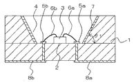
【解決手段】発光素子収納用パッケージは、絶縁基体1の上面に、内周面が上側に向かって外側に広がるように傾斜しているとともに平面視形状が一方向に長い形状である凹部4が形成されており、凹部4の底面の中央部に発光素子3が搭載される搭載部2が形成され、かつ搭載部2に隣接して発光素子3の電極が接続される配線層5が形成されているものであって、凹部4は、内周面の一方向で対向している部位の傾斜角度θ1が一方向に直交する方向で対向している部位の傾斜角度θ2よりも小さくなっている。
【選択図】 図1An object of the present invention is to be able to satisfactorily reflect light from a light emitting element and uniformly and efficiently radiate the light to the outside.
A light emitting element housing package includes a concave portion (4) on an upper surface of an insulating base (1), the inner peripheral surface of which is inclined so as to expand outward toward the upper side, and has a shape that is long in one direction when viewed in plan. The mounting portion 2 on which the light emitting element 3 is mounted is formed at the center of the bottom surface of the concave portion 4, and the wiring layer 5 adjacent to the mounting portion 2 to which the electrode of the light emitting element 3 is connected is formed. In the recess 4, the inclination angle θ 1 of the portion facing the inner peripheral surface in one direction is smaller than the inclination angle θ 2 of the portion facing the direction perpendicular to the one direction. ing.
[Selection diagram] Fig. 1
Description
【0001】
【発明の属する技術分野】
本発明は、発光ダイオード等の発光素子を用いた表示装置等に用いられる、発光素子を収納するための発光素子収納用パッケージおよび発光装置に関する。
【0002】
【従来の技術】
従来、発光ダイオード等の発光素子を収納するための発光素子収納用パッケージ(以下、単にパッケージともいう)として、セラミック製のパッケージが用いられており、その一例を図8に示す(例えば、下記の特許文献1参照)。同図に示すように、従来のパッケージは、複数のセラミック層が積層されて成るとともに上面に凹部14が形成されている直方体状の絶縁基体の凹部14の底面に発光素子13を搭載するため搭載部としての導体層12が設けられた基体11と、基体11の導体層12およびその周辺から基体11の下面に形成された一対の配線層15とから主に構成されている。
【0003】
そして、一方の配線層15の一端が電気的に接続された導体層12上に発光素子13を導電性接着剤、半田等を介して載置固定するとともに、発光素子13の電極と他方の配線層15とをボンディングワイヤ16を介して電気的に接続し、しかる後、基体11の凹部14内に図示しない透明樹脂を充填して発光素子13を封止することによって、発光装置が作製される。
【0004】
また、凹部14の内周面で発光素子13の光を反射させてパッケージの上方に光を放射させるために、凹部14の内周面にニッケル(Ni)めっき層や金(Au)めっき層を表面に有するメタライズ層からなる金属層17を被着させていることもある。
【0005】
また、上記のパッケージはセラミックグリーンシート積層法により以下のようにして製作される。まず、基体11の導体層12(導体層12から下側)を形成するためのセラミックグリーンシート(以下、グリーンシートともいう)と、基体11の凹部14を形成するためのグリーンシートとを準備し、これらのグリーンシートに配線導体15を導出させるための貫通孔や凹部14となる貫通穴を打ち抜き法で形成する。
【0006】
次に、導体層12を形成するためのグリーンシートの積層体Aの貫通孔および所定の部位に、メタライズ層から成る配線層15形成用の導体ペーストをスクリーン印刷法等で印刷塗布し、また凹部14の内周面にメタライズ層を被着する場合、凹部14を形成するためのグリーンシートの積層体Bの貫通穴内面に金属層17形成用の導体ペーストをスクリーン印刷法等で印刷塗布する。
【0007】
次に、積層体A,Bを重ねて接着して基体11を形成するための積層体とし、これを所定寸法に切断して成形体となし、高温(1600℃程度)で焼成して焼結体となす。その後、配線層15および金属層17の露出表面にニッケル,金,パラジウム,白金等の金属から成るめっき金属層を無電解めっき法や電解めっき法により被着させることによって、パッケージが製作される。
【0008】
【特許文献1】
特開2002−232017号公報
【0009】
【発明が解決しようとする課題】
しかしながら、上記従来のパッケージにおいては、近年のパッケージの小型化に伴い、凹部14の底面の発光素子13の搭載領域や配線層15の領域が非常に狭くなってきており、導体層12および配線層15と、凹部14の内周面の金属層17とが短絡する危険性が高くなるという問題点を有していた。
【0010】
そのために、短絡を防止するために、凹部14の底面上の発光素子13の搭載領域や配線層15の領域を広くする必要があり、パッケージを極度に大きくすることなく、凹部14の底面上の発光素子13の搭載領域や配線層15の領域を大きくするために、凹部14を平面視で一方向に長い形状とすることがある。
【0011】
しかしながら、凹部14が一方向に長い形状であると、発光素子13が発光する光を金属層17にて満遍なく均一に反射するのが困難になるという問題点を有していた。
【0012】
従って、本発明は上記従来の技術の問題点に鑑み完成されたものであり、その目的は、凹部内に収容された発光素子が発光する光を効率良く反射させて、均一かつ良好に外部に放射することができる発光素子収納用パッケージおよび発光装置を提供することにある。
【0013】
【課題を解決するための手段】
本発明の発光素子収納用パッケージは、絶縁基体の上面に、内周面が上側に向かって外側に広がるように傾斜しているとともに平面視形状が一方向に長い形状である凹部が形成されており、該凹部の底面の中央部に発光素子が搭載される搭載部が形成され、かつ該搭載部に隣接して前記発光素子の電極が接続される配線層が形成されている発光素子収納用パッケージであって、前記凹部は、内周面の前記一方向で対向している部位の傾斜角度が前記一方向に直交する方向で対向している部位の傾斜角度よりも小さいことを特徴とする。
【0014】
本発明の発光素子収納用パッケージは、凹部は、内周面の一方向で対向している部位の傾斜角度が一方向に直交する方向で対向している部位の傾斜角度よりも小さいことから、内周面の一方向で対向している部位における発光素子の光の金属層による反射光の絶縁基体上面に対する方向と、内周面の一方向に直交する方向で対向している部位における発光素子の光の金属層による反射光の絶縁基体上面に対する方向とを近くすることができるので、凹部の底面の中央部に搭載される発光素子が発光する光を良好に反射し、均一かつ効率よく外部に放射することができる。
【0015】
本発明の発光装置は、本発明の発光素子収納用パッケージと、前記搭載部に搭載されるとともに前記配線層に電極が電気的に接続された発光素子と、該発光素子を覆う透明樹脂とを具備していることを特徴とする。
【0016】
本発明の発光装置は、上記の構成により、発光素子の光を良好に反射し、外部に均一かつ効率良く外部に放射することができる、発光効率の高い高性能のものとなる。
【0017】
【発明の実施の形態】
本発明の発光素子収納用パッケージを以下に詳細に説明する。図1は本発明のパッケージについて実施の形態の一例を示す平面図であり、図2は図1のパッケージのX−X線における断面図、図3は図1のパッケージのY−Y線における断面図である。これらの図において、1は絶縁基体、2は発光素子3の搭載部、3は発光素子、4は発光素子3を収容するための凹部である。
【0018】
本発明の発光素子収納用パッケージは、絶縁基体1の上面に、内周面が上側に向かって外側に広がるように傾斜しているとともに平面視形状が一方向に長い形状である凹部4が形成されており、凹部4の底面の中央部に発光素子3が搭載される搭載部2が形成され、かつ搭載部2に隣接して発光素子3の電極が接続される配線層5が形成されているものであって、凹部4は、内周面の一方向で対向している部位の傾斜角度θ1が一方向に直交する方向で対向している部位の傾斜角度θ2よりも小さくなっている。
【0019】
なお、傾斜角度θ1,θ2は、凹部4の底面に対する凹部4の内周面の傾斜角度である。
【0020】
本発明における絶縁基体1は、セラミックスや樹脂から成り、セラミックスからなる場合、例えば酸化アルミニウム質焼結体(アルミナセラミックス),窒化アルミニウム質焼結体,ムライト質焼結体,ガラスセラミックス質焼結体等のセラミックスから成る絶縁層を複数層積層してなる直方体状の箱状であり、上面の中央部に発光素子3を収容するための凹部4が形成されている。絶縁基体1が例えば酸化アルミニウム質焼結体から成る場合、酸化アルミニウム、酸化珪素、酸化マグネシウム、酸化カルシウム等の原料粉末に適当な有機バインダー、溶剤等を添加混合して泥漿状となし、これを従来周知のドクターブレード法やカレンダーロール法等によりシート状に成形してグリーンシート(セラミック生シート)を得、しかる後、グリーンシートに凹部4用の貫通孔を打ち抜き加工で形成するとともに、発光素子3を搭載するためのグリーンシートと凹部4用のグリーンシートとを複数枚積層し、高温(約1600℃)で焼成し一体化することで形成される。
【0021】
また、凹部4の底面の中央部には発光素子3が搭載される搭載部2が形成され、その周辺には発光素子3の電極と接続される配線層5が形成されている。搭載部2が導体層から成る場合、搭載部2および配線層5はタングステン(W),モリブデン(Mo),銅(Cu),銀(Ag)等の金属粉末のメタライズ層から成っている。
【0022】
また、絶縁基体1には、搭載部2および配線層5に電気的に接続され、絶縁基体1の下面または側面に形成された配線導体8a,8bが被着形成されている。配線導体8a,8bは、WやMo等の金属粉末のメタライズ層から成り、凹部4に収容された発光素子3を外部に電気的に接続するための導電路である。そして、搭載部2には発光ダイオード(LED),半導体レーザ(LD)等の発光素子3が金(Au)−シリコン(Si)合金やAg−エポキシ樹脂等の導電性接合材により固着されるとともに、配線層5には発光素子3の電極がボンディングワイヤ6を介して電気的に接続されている。そして、絶縁基体1の配線導体8a,8bが外部電気回路基板の配線導体に接続されることで発光素子3の各電極と電気的に接続され、発光素子3へ電力や駆動信号が供給される。
【0023】
搭載部2、配線層5および配線導体8a,8bは、例えばWやMo等の金属粉末に適当な有機溶剤、溶媒を添加混合して得た金属ペーストを、絶縁基体1となるグリーンシートに予めスクリーン印刷法により所定パターンに印刷塗布しておくことによって、絶縁基体1の所定位置に被着形成される。
【0024】
なお、搭載部2、配線層5および配線導体8a,8bの露出する表面に、ニッケル(Ni),金(Au),Ag等の耐蝕性に優れる金属を1〜20μm程度の厚みで被着させておくのがよく、搭載部2、配線層5および配線導体8a,8bが酸化腐蝕するのを有効に防止できるとともに、搭載部2と発光素子3との固着、配線層5とボンディングワイヤ6との接合、および配線導体8a,8bと外部電気回路基板の配線導体との接合を強固にすることができる。従って、搭載部2、配線層5および配線導体8a,8bの露出表面には、厚さ1〜10μm程度のNiめっき層と厚さ0.1〜3μm程度のAuめっき層またはAgめっき層とが、電解めっき法や無電解めっき法により順次被着されていることがより好ましい。
【0025】
また、凹部4の内周面には、メタライズ金属層および発光素子3が発光する光に対する反射率が80%以上である金属めっき層を被着した金属層7が形成されていることが好ましい。この金属層7は、例えば、WやMo等から成るメタライズ金属層上にNi,Au,Ag等の金属めっき層を被着させて成り、これにより発光素子3が発光する光に対する反射率を80%以上とすることができる。発光素子3が発光する光に対する反射率が80%未満であると、凹部4に収容された発光素子3が発光する光を良好に反射することが困難となる。
【0026】
また、金属層7は、Au,Ag,アルミニウム等の金属を凹部4の内周面に蒸着により被着したものや、Au,Ag,アルミニウム等の金属板や金属箔を凹部4の内周面に取着したものであっても良い。
【0027】
また、凹部4の内周面は、凹部4の底面から絶縁基体1の上面に向けて外側に広がった傾斜面となっており、特に、35〜70°の角度で外側に広がっていることが好ましい。角度θ1,θ2が70°を超えると、凹部4内に収容された発光素子3が発光する光を外部に対して良好に反射することが困難となる傾向にある。一方、角度θ1,θ2が35°未満であると、凹部4の内周面をそのような角度で安定かつ効率良く形成することが困難となる傾向にあるとともに、パッケージが大型化してしまう。
【0028】
また、凹部4は平面視形状が一方向に長い形状である、長円形状、楕円形状、長方形状、多角形状とされており、例えば図4は凹部4の平面視形状が長方形状であるパッケージの平面図である。本発明のパッケージにおいて、発光素子3の反射に影響を与えずクラック等の破損の発生を防ぐうえで、凹部4はその内周面に角部がない長円形状、楕円形状が好ましい。
【0029】
また、凹部4の内周面の金属層7の表面の算術平均粗さはRaは3μm以下が好ましい。3μmを超えると、凹部4内に収容された発光素子3が発光する光が散乱し、反射光を高い反射率で外部に均一に放射することが困難になる。
【0030】
そして、本発明において、凹部4は、内周面の一方向で対向している部位の傾斜角度θ1が一方向に直交する方向で対向している部位の傾斜角度θ2よりも小さくなっている。これにより、内周面の一方向で対向している部位における発光素子3の光の金属層7による反射光の絶縁基体1上面に対する方向と、内周面の一方向に直交する方向で対向している部位における発光素子3の光の金属層7による反射光の絶縁基体1上面に対する方向とを近くすることができるので、凹部4の底面の中央部に搭載された発光素子3の光を良好に反射し、均一かつ効率よく外部に放射することができる。
【0031】
このような作用を図5を用いて説明する。図5(a)は、内周面の一方向で対向している部位(部位Xとする)における発光素子3の光の反射光の様子について説明する部分断面図であり、図5(b)は、内周面の一方向に直交する方向で対向している部位(部位Yとする)における発光素子3の光の反射光の様子について説明する部分断面図である。同図において、A−A’線は、凹部4の内周面の反射点を通る線で凹部4の底面からのある高さを示す線であり、B−B’線およびC−C’線は、A−A’線の高さにおける部位X,Yで反射された発光素子3の光の光軸を示す線である。また、θ3,θ4は、発光素子3の反射光の光軸とA−A’線(凹部4の底面)との成す角度である。
【0032】
この場合、内周面の部位Yは部位Xよりも発光素子3の近くにあるので、内周面の傾斜角度θ1,θ2が同じであると、部位Yで発光素子3の光の金属層7への入射角度(内周面の法線に対する角度)が大きくなり、反射光は部位Yで部位Xよりも外側に広がりやすくなる。したがって、部位Yの傾斜角度θ2を部位Xの傾斜角度θ1よりも大きくすることで、部位Yにおける発光素子3の光の反射光が外側に広がるのを防ぐことができ、部位X,Yにおける発光素子3の光の金属層7による反射光の方向を近似させることができる。
【0033】
なお、部位X,Yにおける発光素子3の光の金属層7による反射光の方向が同じになるように、傾斜角度θ1,θ2を調整することがより好ましい。これにより、発光素子3の光の金属層7での反射光をより均一に放射することができる。この場合、凹部4の底面の中心部に配置された発光素子3の発光部の中心から上方に発光する光の方向が、絶縁基体1の上面と凹部4の底面との中間の高さにおける金属層7による反射光の方向と同じとなるように、傾斜角度θ1,θ2を調整するのが良い。
【0034】
また、部位Xおよびその周囲の凹部4の内周面と、部位Yおよびその周囲の凹部4の内周面とで、表面粗さや金属層7が異なるようにして、部位X,Y間で反射率が異なるようにしても良い。例えば、部位Xおよびその周囲の凹部4の内周面の面積は、部位Yおよびその周囲の凹部4の内周面の面積よりも大きく、部位Xおよびその周囲では、発光素子3の発光する光に対する単位面積当たりの照射光量が小さくなりやすい。したがって、部位Yおよびその周囲の凹部4の内周面について、その表面粗さを粗くしたりして、部位Xおよびその周囲の凹部4の内周面よりも反射率を低くすることで、部位X,Y間で反射光の強度を近似させて、光が外部に均一に放射されるようにしても良い。
【0035】
本発明の発光装置は、本発明のパッケージと、搭載部2に搭載されるとともに配線層5に電気的に接続された発光素子3と、発光素子3を覆うシリコーン樹脂等の透明樹脂とを具備している。これにより、発光素子3の光を良好に反射し、外部に均一かつ効率良く外部に放射することができる、発光効率の高い高性能のものとなる。発光素子3を覆う透明樹脂は、発光素子3およびその周囲のみを覆っていてもよいし、凹部4内に充填されて発光素子3を覆っていてもよい。
【0036】
なお、本発明は上述の実施の形態に限定されず、本発明の要旨を逸脱しない範囲内で種々の変更を施すことは何等差し支えない。例えば、搭載部2が導体層として形成されていない場合、搭載部2の周辺に配線導体8a,8bにそれぞれ電気的に接続された配線層5a,5bを形成し、発光素子3を凹部4の中央部にフリップチップ実装により配線層5a,5bに接続してもよい。また、図6のパッケージの断面図、図6のパッケージの平面図である図7に示すように、発光素子3を搭載部2となる凹部4の底面の中央部に樹脂接着剤等により接合して搭載されるものとし、発光素子3の電極をボンディングワイヤ6a,6bを介して、配線層5a,5bに電気的に接続されるようにしていても良い。また、複数の発光素子3が凹部4の底面の中央部の搭載部2に搭載されるものであって、複数の発光素子3の電極に接続される多数の配線層5が形成されたものであっても良い。
【0037】
【発明の効果】
本発明の発光素子収納用パッケージは、絶縁基体の上面に形成された凹部は、内周面の一方向で対向している部位の傾斜角度が一方向に直交する方向で対向している部位の傾斜角度よりも小さいことから、内周面の一方向で対向している部位における発光素子の光の金属層による反射光の絶縁基体上面に対する方向と、内周面の一方向に直交する方向で対向している部位における発光素子の光の金属層による反射光の絶縁基体上面に対する方向とを近くすることができるので、凹部の底面の中央部に搭載される発光素子が発光する光を良好に反射し、均一かつ効率よく外部に放射することができる。
【0038】
本発明の発光装置は、本発明の発光素子収納用パッケージと、搭載部に搭載されるとともに配線層に電極が電気的に接続された発光素子と、発光素子を覆う透明樹脂とを具備していることにより、発光素子の光を良好に反射し、外部に均一かつ効率良く外部に放射することができる、発光効率の高い高性能のものとなる。
【図面の簡単な説明】
【図1】本発明の発光素子収納用パッケージについて実施の形態の一例を示す平面図である。
【図2】図1の発光素子収納用パッケージのX−X線における断面図である。
【図3】図1の発光素子収納用パッケージのY−Y線における断面図である。
【図4】本発明の発光素子収納用パッケージについて実施の形態の他の例を示す平面図である。
【図5】(a)は凹部の内周面の一方向で対向している部位における発光素子の光の反射の様子を示す凹部の部分拡大断面図、(b)は凹部の内周面の一方向の直交する方向で対向している部位における発光素子の光の反射の様子を示す凹部の部分拡大断面図である。
【図6】本発明の発光素子収納用パッケージについて実施の形態の他の例を示す断面図である。
【図7】図6の発光素子収納用パッケージの平面図である。
【図8】従来の発光素子収納用パッケージの断面図である。
【符号の説明】
1:絶縁基体
2:搭載部
3:発光素子
4:凹部
5:配線層
8a,8b:配線導体[0001]
TECHNICAL FIELD OF THE INVENTION
The present invention relates to a light emitting element housing package for housing a light emitting element and a light emitting device used for a display device or the like using a light emitting element such as a light emitting diode.
[0002]
[Prior art]
2. Description of the Related Art Conventionally, a ceramic package has been used as a light emitting element housing package (hereinafter, also simply referred to as a package) for housing a light emitting element such as a light emitting diode, and an example thereof is shown in FIG. Patent Document 1). As shown in the drawing, the conventional package is formed by stacking a plurality of ceramic layers and mounting the
[0003]
Then, the
[0004]
In order to reflect the light of the
[0005]
The above package is manufactured by the ceramic green sheet laminating method as follows. First, a ceramic green sheet (hereinafter, also referred to as a green sheet) for forming the conductor layer 12 (below the conductor layer 12) of the
[0006]
Next, a conductor paste for forming a
[0007]
Next, the laminates A and B are overlapped and bonded to form a laminate for forming the
[0008]
[Patent Document 1]
JP-A-2002-232017
[Problems to be solved by the invention]
However, in the conventional package described above, the mounting area of the
[0010]
Therefore, in order to prevent a short circuit, the mounting area of the
[0011]
However, when the
[0012]
Accordingly, the present invention has been completed in view of the problems of the above-described conventional technology, and an object of the present invention is to efficiently and efficiently reflect light emitted by a light emitting element housed in a concave portion to the outside. An object of the present invention is to provide a light emitting element housing package and a light emitting device that can emit light.
[0013]
[Means for Solving the Problems]
In the light emitting element housing package of the present invention, a concave portion is formed on the upper surface of the insulating base, the concave portion being inclined so that the inner peripheral surface expands outward toward the upper side and having a shape in a plan view that is long in one direction. A mounting portion for mounting the light emitting element is formed at the center of the bottom surface of the concave portion, and a wiring layer to which an electrode of the light emitting device is connected is formed adjacent to the mounting portion, for housing the light emitting element. The package, wherein the concave portion has a smaller inclination angle of a portion of the inner peripheral surface facing the one direction in the direction orthogonal to the one direction. .
[0014]
In the light-emitting element housing package of the present invention, since the concave portion has a smaller inclination angle of a portion facing in one direction of the inner peripheral surface than a tilt angle of a portion facing in a direction orthogonal to one direction, A light emitting element at a portion opposed in a direction orthogonal to one direction of the inner peripheral surface with respect to a direction of light reflected by the metal layer of the light emitting element at a portion opposed in one direction of the inner peripheral surface to the upper surface of the insulating base. Since the direction of the light reflected by the metal layer with respect to the upper surface of the insulating substrate can be made closer, the light emitted by the light emitting element mounted at the center of the bottom surface of the concave portion can be reflected well, and uniform and efficient external light can be reflected. Can be radiated.
[0015]
The light-emitting device of the present invention includes the light-emitting element housing package of the present invention, a light-emitting element mounted on the mounting portion and having an electrode electrically connected to the wiring layer, and a transparent resin covering the light-emitting element. It is characterized by having.
[0016]
With the above structure, the light emitting device of the present invention has high luminous efficiency and high performance, which can satisfactorily reflect the light of the light emitting element and radiate the light uniformly and efficiently to the outside.
[0017]
BEST MODE FOR CARRYING OUT THE INVENTION
The light emitting element housing package of the present invention will be described in detail below. 1 is a plan view showing an example of an embodiment of the package of the present invention. FIG. 2 is a cross-sectional view of the package of FIG. 1 taken along line XX. FIG. 3 is a cross-sectional view of the package of FIG. FIG. In these figures, 1 is an insulating base, 2 is a mounting portion of the
[0018]
In the light-emitting element housing package of the present invention, a
[0019]
The inclination angles θ 1 and θ 2 are the inclination angles of the inner peripheral surface of the
[0020]
The insulating
[0021]
A mounting
[0022]
In addition,
[0023]
The mounting
[0024]
A metal having excellent corrosion resistance, such as nickel (Ni), gold (Au), or Ag, is applied to the exposed surfaces of the mounting
[0025]
Further, it is preferable that a
[0026]
The
[0027]
Further, the inner peripheral surface of the
[0028]
The
[0029]
The arithmetic average roughness Ra of the surface of the
[0030]
Then, in the present invention, the
[0031]
Such an operation will be described with reference to FIG. FIG. 5A is a partial cross-sectional view illustrating a state of reflected light of light from the
[0032]
In this case, since the part Y on the inner peripheral surface is closer to the
[0033]
It is more preferable to adjust the inclination angles θ 1 and θ 2 so that the directions of the light reflected by the
[0034]
Further, the surface roughness and the
[0035]
The light emitting device of the present invention includes the package of the present invention, a
[0036]
Note that the present invention is not limited to the above-described embodiment, and various changes may be made without departing from the spirit of the present invention. For example, when the mounting
[0037]
【The invention's effect】
In the light-emitting element housing package of the present invention, the concave portion formed on the upper surface of the insulating base has a portion in which the inclination angle of the portion facing in one direction of the inner peripheral surface is opposed in a direction orthogonal to one direction. Since it is smaller than the inclination angle, the direction of the light reflected by the metal layer of the light of the light emitting element at the portion opposed in one direction of the inner peripheral surface to the upper surface of the insulating base and the direction orthogonal to one direction of the inner peripheral surface. Since the direction of the light reflected by the metal layer of the light emitting element at the opposing portion can be close to the direction with respect to the upper surface of the insulating base, the light emitted by the light emitting element mounted at the center of the bottom surface of the concave portion can be improved. It can reflect and radiate uniformly and efficiently to the outside.
[0038]
The light-emitting device of the present invention includes the light-emitting element housing package of the present invention, a light-emitting element mounted on a mounting portion and having an electrode electrically connected to a wiring layer, and a transparent resin covering the light-emitting element. Accordingly, the light from the light emitting element can be satisfactorily reflected, and can be uniformly and efficiently radiated to the outside.
[Brief description of the drawings]
FIG. 1 is a plan view showing an example of an embodiment of a light emitting element housing package of the present invention.
FIG. 2 is a cross-sectional view of the light emitting element housing package of FIG. 1 taken along line XX.
FIG. 3 is a cross-sectional view of the light emitting element housing package of FIG. 1 taken along line YY.
FIG. 4 is a plan view showing another example of the embodiment of the light emitting element housing package of the present invention.
FIG. 5A is a partially enlarged cross-sectional view of a concave portion showing a state of light reflection of a light emitting element at a portion facing the inner peripheral surface of the concave portion in one direction, and FIG. FIG. 4 is a partially enlarged cross-sectional view of a recess showing a state of light reflection of a light emitting element in a portion facing in a direction orthogonal to one direction.
FIG. 6 is a cross-sectional view showing another example of the embodiment of the light emitting element housing package of the present invention.
FIG. 7 is a plan view of the light emitting element housing package of FIG. 6;
FIG. 8 is a cross-sectional view of a conventional light emitting element storage package.
[Explanation of symbols]
1: Insulating base 2: Mounting part 3: Light emitting element 4: Depression 5:
Claims (2)
Priority Applications (1)
| Application Number | Priority Date | Filing Date | Title |
|---|---|---|---|
| JP2003080126A JP4132039B2 (en) | 2003-03-24 | 2003-03-24 | Light emitting element storage package and light emitting device |
Applications Claiming Priority (1)
| Application Number | Priority Date | Filing Date | Title |
|---|---|---|---|
| JP2003080126A JP4132039B2 (en) | 2003-03-24 | 2003-03-24 | Light emitting element storage package and light emitting device |
Publications (2)
| Publication Number | Publication Date |
|---|---|
| JP2004288936A true JP2004288936A (en) | 2004-10-14 |
| JP4132039B2 JP4132039B2 (en) | 2008-08-13 |
Family
ID=33294069
Family Applications (1)
| Application Number | Title | Priority Date | Filing Date |
|---|---|---|---|
| JP2003080126A Expired - Fee Related JP4132039B2 (en) | 2003-03-24 | 2003-03-24 | Light emitting element storage package and light emitting device |
Country Status (1)
| Country | Link |
|---|---|
| JP (1) | JP4132039B2 (en) |
Cited By (6)
| Publication number | Priority date | Publication date | Assignee | Title |
|---|---|---|---|---|
| JP2006114854A (en) * | 2004-10-18 | 2006-04-27 | Sharp Corp | Backlight device for semiconductor light emitting device and liquid crystal display device |
| JP2006210627A (en) * | 2005-01-27 | 2006-08-10 | Kyocera Corp | Light emitting element storage package, light emitting device, and lighting device |
| JP2009206466A (en) * | 2008-01-30 | 2009-09-10 | Kyocera Corp | Package for storing light emitting element, and light emitting device |
| JP2015092639A (en) * | 2007-04-19 | 2015-05-14 | エルジー イノテック カンパニー リミテッド | Light emitting device package and light unit having the same |
| WO2016194120A1 (en) * | 2015-06-01 | 2016-12-08 | 三菱電機株式会社 | Light emitting device, display unit, and image display device |
| CN113711349A (en) * | 2019-04-25 | 2021-11-26 | 京瓷株式会社 | Substrate for mounting light-emitting element and light-emitting device |
-
2003
- 2003-03-24 JP JP2003080126A patent/JP4132039B2/en not_active Expired - Fee Related
Cited By (14)
| Publication number | Priority date | Publication date | Assignee | Title |
|---|---|---|---|---|
| US7977689B2 (en) | 2004-10-18 | 2011-07-12 | Sharp Kabushiki Kaisha | Backlight device for liquid crystal display including a plurality of light emitting diodes within their own concaves aligned in a straight line within a larger concave |
| JP2006114854A (en) * | 2004-10-18 | 2006-04-27 | Sharp Corp | Backlight device for semiconductor light emitting device and liquid crystal display device |
| JP2006210627A (en) * | 2005-01-27 | 2006-08-10 | Kyocera Corp | Light emitting element storage package, light emitting device, and lighting device |
| US9559275B2 (en) | 2007-04-19 | 2017-01-31 | Lg Innotek Co., Ltd. | Light emitting device package and light unit having the same |
| JP2015092639A (en) * | 2007-04-19 | 2015-05-14 | エルジー イノテック カンパニー リミテッド | Light emitting device package and light unit having the same |
| US9666775B2 (en) | 2007-04-19 | 2017-05-30 | Lg Innotek Co., Ltd. | Light emitting device package and light unit having the same |
| JP2009206466A (en) * | 2008-01-30 | 2009-09-10 | Kyocera Corp | Package for storing light emitting element, and light emitting device |
| WO2016194120A1 (en) * | 2015-06-01 | 2016-12-08 | 三菱電機株式会社 | Light emitting device, display unit, and image display device |
| JPWO2016194120A1 (en) * | 2015-06-01 | 2017-08-24 | 三菱電機株式会社 | Light emitting device, display unit, and video display device |
| CN107615499A (en) * | 2015-06-01 | 2018-01-19 | 三菱电机株式会社 | Light-emitting device, display unit and video display devices |
| EP3306683A4 (en) * | 2015-06-01 | 2018-12-19 | Mitsubishi Electric Corporation | Light emitting device, display unit, and image display device |
| US10256383B2 (en) | 2015-06-01 | 2019-04-09 | Mitsubishi Electric Corporation | Light emitting device with dark area and greater reflectance light area, display unit, and image display device |
| CN107615499B (en) * | 2015-06-01 | 2020-01-24 | 三菱电机株式会社 | Light emitting device, display unit, and video display device |
| CN113711349A (en) * | 2019-04-25 | 2021-11-26 | 京瓷株式会社 | Substrate for mounting light-emitting element and light-emitting device |
Also Published As
| Publication number | Publication date |
|---|---|
| JP4132039B2 (en) | 2008-08-13 |
Similar Documents
| Publication | Publication Date | Title |
|---|---|---|
| JP4070208B2 (en) | Light emitting element storage package and light emitting device | |
| JP2004253404A (en) | Light emitting element storage package and light emitting device | |
| JP4072084B2 (en) | Light emitting element storage package and light emitting device | |
| JP2004207621A (en) | Light emitting element storage package and light emitting device | |
| JP2004281994A (en) | Light emitting element storage package and light emitting device | |
| JP2004319939A (en) | Light emitting element storage package and light emitting device | |
| JP4307090B2 (en) | Light emitting element storage package and light emitting device | |
| JP4132038B2 (en) | Light emitting device | |
| JP4295519B2 (en) | Light emitting element storage package and light emitting device | |
| JP2005191111A (en) | Light emitting element storage package and light emitting device | |
| JP2004207542A (en) | Light emitting element storage package and light emitting device | |
| JP4132043B2 (en) | Light emitting element storage package and light emitting device | |
| JP2005019688A (en) | Light emitting element storage package and light emitting device | |
| JP4164006B2 (en) | Light emitting element storage package and light emitting device | |
| JP2004259893A (en) | Light emitting element storage package and light emitting device | |
| JP4336136B2 (en) | Light emitting element storage package and light emitting device | |
| JP4336153B2 (en) | Light emitting element storage package and light emitting device | |
| JP4132039B2 (en) | Light emitting element storage package and light emitting device | |
| JP5173903B2 (en) | Light emitting element storage package and light emitting device | |
| JP2004200410A (en) | Light emitting element storage package and light emitting device | |
| JP4336137B2 (en) | Light emitting element storage package and light emitting device | |
| JP4070195B2 (en) | Light emitting element storage package | |
| JP4183175B2 (en) | Light emitting element storage package and light emitting device | |
| JP2004311916A (en) | Light emitting element storage package and light emitting device | |
| JP2005159082A (en) | Light emitting element storage package, light emitting device, and method of manufacturing light emitting element storage package |
Legal Events
| Date | Code | Title | Description |
|---|---|---|---|
| A621 | Written request for application examination |
Free format text: JAPANESE INTERMEDIATE CODE: A621 Effective date: 20060307 |
|
| A131 | Notification of reasons for refusal |
Free format text: JAPANESE INTERMEDIATE CODE: A131 Effective date: 20071210 |
|
| A521 | Request for written amendment filed |
Free format text: JAPANESE INTERMEDIATE CODE: A523 Effective date: 20080206 |
|
| TRDD | Decision of grant or rejection written | ||
| A01 | Written decision to grant a patent or to grant a registration (utility model) |
Free format text: JAPANESE INTERMEDIATE CODE: A01 Effective date: 20080507 |
|
| A01 | Written decision to grant a patent or to grant a registration (utility model) |
Free format text: JAPANESE INTERMEDIATE CODE: A01 |
|
| A61 | First payment of annual fees (during grant procedure) |
Free format text: JAPANESE INTERMEDIATE CODE: A61 Effective date: 20080530 |
|
| FPAY | Renewal fee payment (event date is renewal date of database) |
Free format text: PAYMENT UNTIL: 20110606 Year of fee payment: 3 |
|
| R150 | Certificate of patent or registration of utility model |
Ref document number: 4132039 Country of ref document: JP Free format text: JAPANESE INTERMEDIATE CODE: R150 Free format text: JAPANESE INTERMEDIATE CODE: R150 |
|
| FPAY | Renewal fee payment (event date is renewal date of database) |
Free format text: PAYMENT UNTIL: 20120606 Year of fee payment: 4 |
|
| FPAY | Renewal fee payment (event date is renewal date of database) |
Free format text: PAYMENT UNTIL: 20120606 Year of fee payment: 4 |
|
| FPAY | Renewal fee payment (event date is renewal date of database) |
Free format text: PAYMENT UNTIL: 20130606 Year of fee payment: 5 |
|
| LAPS | Cancellation because of no payment of annual fees |