JP2004281380A - Display device and method of manufacturing the same - Google Patents
Display device and method of manufacturing the same Download PDFInfo
- Publication number
- JP2004281380A JP2004281380A JP2004010345A JP2004010345A JP2004281380A JP 2004281380 A JP2004281380 A JP 2004281380A JP 2004010345 A JP2004010345 A JP 2004010345A JP 2004010345 A JP2004010345 A JP 2004010345A JP 2004281380 A JP2004281380 A JP 2004281380A
- Authority
- JP
- Japan
- Prior art keywords
- layer
- light emitting
- panel
- display device
- electrode
- Prior art date
- Legal status (The legal status is an assumption and is not a legal conclusion. Google has not performed a legal analysis and makes no representation as to the accuracy of the status listed.)
- Granted
Links
Images


Classifications
-
- H—ELECTRICITY
- H10—SEMICONDUCTOR DEVICES; ELECTRIC SOLID-STATE DEVICES NOT OTHERWISE PROVIDED FOR
- H10K—ORGANIC ELECTRIC SOLID-STATE DEVICES
- H10K59/00—Integrated devices, or assemblies of multiple devices, comprising at least one organic light-emitting element covered by group H10K50/00
- H10K59/80—Constructional details
- H10K59/87—Passivation; Containers; Encapsulations
- H10K59/871—Self-supporting sealing arrangements
- H10K59/8722—Peripheral sealing arrangements, e.g. adhesives, sealants
-
- E—FIXED CONSTRUCTIONS
- E06—DOORS, WINDOWS, SHUTTERS, OR ROLLER BLINDS IN GENERAL; LADDERS
- E06B—FIXED OR MOVABLE CLOSURES FOR OPENINGS IN BUILDINGS, VEHICLES, FENCES OR LIKE ENCLOSURES IN GENERAL, e.g. DOORS, WINDOWS, BLINDS, GATES
- E06B9/00—Screening or protective devices for wall or similar openings, with or without operating or securing mechanisms; Closures of similar construction
- E06B9/24—Screens or other constructions affording protection against light, especially against sunshine; Similar screens for privacy or appearance; Slat blinds
- E06B9/26—Lamellar or like blinds, e.g. venetian blinds
- E06B9/262—Lamellar or like blinds, e.g. venetian blinds with flexibly-interconnected horizontal or vertical strips; Concertina blinds, i.e. upwardly folding flexible screens
-
- H—ELECTRICITY
- H10—SEMICONDUCTOR DEVICES; ELECTRIC SOLID-STATE DEVICES NOT OTHERWISE PROVIDED FOR
- H10K—ORGANIC ELECTRIC SOLID-STATE DEVICES
- H10K50/00—Organic light-emitting devices
- H10K50/80—Constructional details
- H10K50/84—Passivation; Containers; Encapsulations
- H10K50/842—Containers
- H10K50/8426—Peripheral sealing arrangements, e.g. adhesives, sealants
-
- H—ELECTRICITY
- H10—SEMICONDUCTOR DEVICES; ELECTRIC SOLID-STATE DEVICES NOT OTHERWISE PROVIDED FOR
- H10K—ORGANIC ELECTRIC SOLID-STATE DEVICES
- H10K50/00—Organic light-emitting devices
- H10K50/80—Constructional details
- H10K50/84—Passivation; Containers; Encapsulations
- H10K50/844—Encapsulations
-
- H—ELECTRICITY
- H10—SEMICONDUCTOR DEVICES; ELECTRIC SOLID-STATE DEVICES NOT OTHERWISE PROVIDED FOR
- H10K—ORGANIC ELECTRIC SOLID-STATE DEVICES
- H10K59/00—Integrated devices, or assemblies of multiple devices, comprising at least one organic light-emitting element covered by group H10K50/00
- H10K59/80—Constructional details
- H10K59/87—Passivation; Containers; Encapsulations
- H10K59/873—Encapsulations
-
- E—FIXED CONSTRUCTIONS
- E06—DOORS, WINDOWS, SHUTTERS, OR ROLLER BLINDS IN GENERAL; LADDERS
- E06B—FIXED OR MOVABLE CLOSURES FOR OPENINGS IN BUILDINGS, VEHICLES, FENCES OR LIKE ENCLOSURES IN GENERAL, e.g. DOORS, WINDOWS, BLINDS, GATES
- E06B9/00—Screening or protective devices for wall or similar openings, with or without operating or securing mechanisms; Closures of similar construction
- E06B9/24—Screens or other constructions affording protection against light, especially against sunshine; Similar screens for privacy or appearance; Slat blinds
- E06B9/26—Lamellar or like blinds, e.g. venetian blinds
- E06B9/262—Lamellar or like blinds, e.g. venetian blinds with flexibly-interconnected horizontal or vertical strips; Concertina blinds, i.e. upwardly folding flexible screens
- E06B2009/2622—Gathered vertically; Roman, Austrian or festoon blinds
-
- E—FIXED CONSTRUCTIONS
- E06—DOORS, WINDOWS, SHUTTERS, OR ROLLER BLINDS IN GENERAL; LADDERS
- E06B—FIXED OR MOVABLE CLOSURES FOR OPENINGS IN BUILDINGS, VEHICLES, FENCES OR LIKE ENCLOSURES IN GENERAL, e.g. DOORS, WINDOWS, BLINDS, GATES
- E06B9/00—Screening or protective devices for wall or similar openings, with or without operating or securing mechanisms; Closures of similar construction
- E06B9/56—Operating, guiding or securing devices or arrangements for roll-type closures; Spring drums; Tape drums; Counterweighting arrangements therefor
- E06B9/78—Operating, guiding or securing devices or arrangements for roll-type closures; Spring drums; Tape drums; Counterweighting arrangements therefor for direct manual operation, e.g. by tassels, by handles
- E06B2009/785—Operating, guiding or securing devices or arrangements for roll-type closures; Spring drums; Tape drums; Counterweighting arrangements therefor for direct manual operation, e.g. by tassels, by handles by belts, straps, bands, tapes, cords, tassels
-
- H—ELECTRICITY
- H10—SEMICONDUCTOR DEVICES; ELECTRIC SOLID-STATE DEVICES NOT OTHERWISE PROVIDED FOR
- H10K—ORGANIC ELECTRIC SOLID-STATE DEVICES
- H10K59/00—Integrated devices, or assemblies of multiple devices, comprising at least one organic light-emitting element covered by group H10K50/00
- H10K59/10—OLED displays
- H10K59/12—Active-matrix OLED [AMOLED] displays
Landscapes
- Engineering & Computer Science (AREA)
- Structural Engineering (AREA)
- Physics & Mathematics (AREA)
- Optics & Photonics (AREA)
- Architecture (AREA)
- Civil Engineering (AREA)
- Electroluminescent Light Sources (AREA)
- Devices For Indicating Variable Information By Combining Individual Elements (AREA)
Abstract
Description
本発明は、発光素子を有する駆動パネルと封止パネルとを中間層を介して対向配置した表示装置およびその製造方法に係り、特に上面発光の有機発光素子を用いた有機発光ディスプレイに好適な表示装置およびその製造方法に関する。 The present invention relates to a display device in which a drive panel having a light-emitting element and a sealing panel are arranged to face each other with an intermediate layer interposed therebetween, and a method for manufacturing the same. The present invention relates to an apparatus and a method for manufacturing the same.
近年、液晶ディスプレイに代わる表示装置として、有機発光素子を用いた有機発光ディスプレイが注目されている。有機発光ディスプレイは、自発光型であるので視野角が広く、消費電力が低いという特性を有し、また、高精細度の高速ビデオ信号に対しても十分な応答性を有するものと考えられており、実用化に向けて開発が進められている。 In recent years, an organic light emitting display using an organic light emitting element has been receiving attention as a display device replacing the liquid crystal display. Organic light-emitting displays are self-luminous and have a wide viewing angle and low power consumption, and are considered to have sufficient responsiveness to high-definition high-speed video signals. It is being developed for practical use.
有機発光ディスプレイでは、例えば、基板上にTFT(Thin Film Transistor;薄膜トランジスタ)などの駆動素子が形成され、この駆動素子の上に、平坦化層を介して有機発光素子が形成されている。平坦化層は、通常は表示領域のみに形成される(例えば、特許文献1参照。)。ただし、平坦化層を表示領域外部、基板の背面の周縁部に保護筐体を接着するためのシールの下まで延在させ、平坦化層をシール硬化時のストレスを吸収する緩衝層として利用するようにした構成もある(例えば、特許文献2参照)。 In an organic light emitting display, for example, a driving element such as a TFT (Thin Film Transistor) is formed on a substrate, and the organic light emitting element is formed on the driving element via a flattening layer. The flattening layer is usually formed only in the display area (for example, see Patent Document 1). However, the flattening layer extends to the outside of the display area, under the seal for bonding the protective housing to the peripheral edge of the back surface of the substrate, and the flattening layer is used as a buffer layer for absorbing stress when the seal is cured. There is also such a configuration (for example, see Patent Document 2).
また、平坦化層の材料については、例えば、有機発光素子への水分の進入を阻止するため、SOG(Spin On Glass )材料など水分を蒸発させる温度に耐えうる膜を採用するようにした提案がある(例えば、特許文献3参照。)。あるいは、エポキシ基を含有するアルカリ可溶性樹脂と1,2−キノンジアジド化合物とを含有する材料を採用することにより、スルーホール等を高解像度で形成できることが報告されている(例えば、特許文献4参照。)。
近年では、高輝度・高開口度の有機発光ディスプレイとして、駆動パネルと封止パネルとを接着層を介して全面にわたって貼り合わせ、有機発光素子により発生した光を封止パネルの側から取り出すようにした上面発光・完全固体封止構造が提案されている。駆動パネルは、例えば、駆動用基板上に、TFT等の駆動素子層およびこれを覆う平坦化層としての被覆層を介して、複数の有機発光素子を有している。 In recent years, as a high-brightness, high-aperture organic light-emitting display, a drive panel and a sealing panel are bonded over the entire surface via an adhesive layer, and light generated by the organic light-emitting element is extracted from the sealing panel side. A top emission and complete solid sealing structure has been proposed. The drive panel has, for example, a plurality of organic light-emitting elements on a drive substrate via a drive element layer such as a TFT and a covering layer as a flattening layer covering the same.
しかしながら、この構造では、被覆層をパターニングすることなく駆動用基板の全面にわたって形成していたので、接着層の端部から被覆層の端部が露出した状態となっていた。そのため、外部の水分が被覆層を経路として侵入し、有機発光素子の劣化の原因となるおそれがあった。 However, in this structure, since the covering layer is formed over the entire surface of the driving substrate without patterning, the end of the covering layer is exposed from the end of the adhesive layer. Therefore, there is a possibility that external moisture may enter through the coating layer as a path and cause deterioration of the organic light emitting device.
本発明はかかる問題点に鑑みてなされたもので、その目的は、被覆層を経由して水分が侵入するのを防止することができ、信頼性を高めた表示装置およびその製造方法を提供することにある。 The present invention has been made in view of such a problem, and an object of the present invention is to provide a display device which can prevent moisture from entering through a coating layer and has improved reliability, and a method for manufacturing the same. It is in.
本発明による表示装置は、駆動用基板上に、駆動素子層および駆動素子層を覆う被覆層を介して、複数の発光素子を有する駆動パネルと、封止用基板を有し、封止用基板が駆動パネルの発光素子側に対向配置された封止パネルと、駆動パネルと封止パネルとの間に複数の発光素子を覆うように設けられると共に、被覆層の表面および端面を覆う中間層とを備えたものである。 The display device according to the present invention includes a driving panel having a plurality of light emitting elements and a sealing substrate on a driving substrate via a driving element layer and a covering layer covering the driving element layer, and a sealing substrate. A sealing panel disposed opposite to the light emitting element side of the driving panel, and an intermediate layer provided between the driving panel and the sealing panel so as to cover the plurality of light emitting elements, and covering a surface and an end surface of the coating layer. It is provided with.
本発明による表示装置の製造方法は、駆動用基板に、駆動素子層および駆動素子層を覆う被覆層を介して複数の発光素子を形成し、駆動パネルを形成する工程と、複数の発光素子および被覆層の表面および端面を覆う中間層を形成する工程と、中間層を介して、駆動パネルの発光素子側に、封止用基板を有する封止パネルを対向配置する工程とを含むものである。 A method for manufacturing a display device according to the present invention includes a step of forming a plurality of light emitting elements on a driving substrate via a driving element layer and a cover layer covering the driving element layer to form a driving panel; The method includes a step of forming an intermediate layer covering the surface and the end face of the coating layer, and a step of disposing a sealing panel having a sealing substrate on the light emitting element side of the drive panel via the intermediate layer.
本発明による表示装置では、中間層が被覆層の表面だけでなく端面をも覆っているので、被覆層の端面が駆動パネルと封止パネルとの間から外部に露出せず、外部の水分が被覆層を経路として発光素子部分へ侵入することがない。 In the display device according to the present invention, since the intermediate layer covers not only the surface of the coating layer but also the end face, the end face of the coating layer is not exposed to the outside from between the drive panel and the sealing panel, and external moisture is not present. It does not enter the light emitting element portion through the coating layer as a route.
本発明による表示装置の製造方法では、駆動用基板に、駆動素子層およびこれを覆う被覆層を介して複数の発光素子が形成され、駆動パネルが形成される。次いで、複数の発光素子および被覆層の表面および端面を覆う中間層が形成される。続いて、中間層を介して、駆動パネルの発光素子側に、封止用基板を有する封止パネルが対向配置される。 In the method of manufacturing a display device according to the present invention, a plurality of light emitting elements are formed on a driving substrate via a driving element layer and a covering layer covering the driving element layer, and a driving panel is formed. Next, an intermediate layer that covers surfaces and end faces of the plurality of light emitting elements and the coating layer is formed. Subsequently, a sealing panel having a sealing substrate is arranged to face the light emitting element side of the drive panel via the intermediate layer.
本発明の表示装置およびその製造方法によれば、駆動パネルと封止パネルとの間の中間層が被覆層の表面だけでなく端面をも覆うように構成したので、被覆層の端面が駆動パネルと封止パネルとの間から外部に露出することがなく、外部の水分が被覆層を経路として内部の素子部分に侵入することがなくなる。よって、素子が劣化することがなくなり、表示装置の信頼性が高まる。 According to the display device and the method of manufacturing the same of the present invention, since the intermediate layer between the drive panel and the sealing panel is configured to cover not only the surface of the coating layer but also the end face, the end face of the coating layer is It is not exposed to the outside from between the sealing panel and the sealing panel, and external moisture does not enter the internal element portion through the coating layer. Therefore, the element does not deteriorate, and the reliability of the display device is improved.
以下、本発明の実施の形態について図面を参照して詳細に説明する。 Hereinafter, embodiments of the present invention will be described in detail with reference to the drawings.
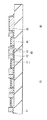
図1は、本発明の一実施の形態に係る表示装置の断面構造を表すものである。この表示装置は、例えば極薄型の有機発光ディスプレイとして用いられるものであり、駆動パネル10と封止パネル20とが対向配置され、駆動パネル10と封止パネル20との間に中間層30が設けられている。駆動パネル10は、例えば、図1(A)に示したように、ガラスなどの絶縁材料よりなる駆動用基板11上に、駆動素子層40およびこの駆動素子層40を覆う被覆層50を介して、赤色の光を発生する有機発光素子10Rと、緑色の光を発生する有機発光素子10Gと、青色の光を発生する有機発光素子10Bとが、順に全体としてマトリクス状に設けられている。また、駆動用基板11の周辺部分には、図1(B)に示したように、周辺回路部60および補助配線70が設けられている。
FIG. 1 illustrates a cross-sectional structure of a display device according to an embodiment of the present invention. This display device is used, for example, as an ultra-thin organic light-emitting display, in which a
有機発光素子10R,10G,10Bは、例えば、駆動用基板11の側から、陽極としての第1電極12、絶縁層13、発光層を含む有機層14、および陰極としての第2電極15がこの順に積層されている。第2電極15は、有機発光素子10R,10G,10Bのすべてを覆う共通電極として形成され、補助配線70の支線70Aに電気的に接続されている。また、第2電極15は、駆動用基板11の周辺部分まで延長され、補助配線70に電気的に接続されている。
In the organic light-
第1電極12は、反射層としての機能も兼ねており、例えば、白金(Pt),金(Au),クロム(Cr)またはタングステン(W)などの金属または合金により構成されている。
The
絶縁層13は、第1電極12と第2電極15との絶縁性を確保すると共に、有機発光素子10R,10G,10Bにおける発光領域の形状を正確に所望の形状とするためのものである。この絶縁層13は、例えば、二酸化ケイ素(SiO2 )などの絶縁材料により構成されている。
The
有機層14は、有機発光素子の発光色によって構成が異なっている。有機発光素子10R,10Bは、正孔輸送層,発光層および電子輸送層が第1電極12の側からこの順に積層された構造を有しており、有機発光素子10Gは、正孔輸送層および発光層が第1電極12の側からこの順に積層された構造を有している。正孔輸送層は、発光層への正孔注入効率を高めるためのものである。発光層は、電界をかけることにより電子と正孔との再結合が起こり、光を発生するものである。電子輸送層は、発光層への電子注入効率を高めるためのものである。
The configuration of the
有機発光素子10Rの正孔輸送層の構成材料としては、例えば、ビス[(N−ナフチル)−N−フェニル]ベンジジン(α−NPD)が挙げられ、有機発光素子10Rの発光層の構成材料としては、例えば、2,5−ビス[4−[N−(4−メトキシフェニル)―N−フェニルアミノ]]スチリルベンゼン―1,4−ジカーボニトリル(BSB)が挙げられ、有機発光素子10Rの電子輸送層の構成材料としては、例えば、8−キノリノールアルミニウム錯体(Alq3 )が挙げられる。
As a constituent material of the hole transport layer of the organic
有機発光素子10Bの正孔輸送層の構成材料としては、例えば、α−NPDが挙げられ、有機発光素子10Bの発光層の構成材料としては、例えば、4,4′−ビス(2,2′−ジフェニルビニン)ビフェニル(DPVBi)が挙げられ、有機発光素子10Bの電子輸送層の構成材料としては、例えば、Alq3 が挙げられる。
As a constituent material of the hole transport layer of the organic
有機発光素子10Gの正孔輸送層の構成材料としては、例えば、α−NPDが挙げられ、有機発光素子10Gの発光層の構成材料としては、例えば、Alq3 にクマリン6(C6;Coumarin6)を1体積%混合したものが挙げられる。
As a constituent material of the hole transport layer of the organic
第2電極15は、半透過性電極により構成されており、発光層で発生した光は第2電極15の側から取り出されるようになっている。第2電極15は、例えば、銀(Ag),アルミニウム(Al),マグネシウム(Mg),カルシウム(Ca),ナトリウム(Na)などの金属または合金により構成されている。
The
封止パネル20は、封止用基板21を有しており、この封止用基板21は、駆動パネル10の有機発光素子10R,10G,10Bの側に配置され、中間層30と共に有機発光素子10R,10G,10Bを封止している。封止用基板21は、有機発光素子10R,10G,10Bで発生した光に対して透明なガラスなどの材料により構成されている。封止用基板21には、例えば、カラーフィルタおよびブラックマトリクスとしての反射光吸収膜(図示せず)が設けられており、有機発光素子10R,10G,10Bで発生した光を取り出すと共に、有機発光素子10R,10G,10Bおよびその間の配線において反射された外光を吸収し、コントラストを改善するようになっている。
The
中間層30は、駆動パネル10と封止パネル20との間に有機発光素子10R,10G,10Bを覆うように設けられると共に、被覆層50の表面50Aおよび端面50Bを覆っている。これにより、この表示装置では、被覆層50の端面が駆動パネル10と封止パネル20との間から外部に露出することがなく、外部の水分が被覆層50を経路として内部の有機発光素子10R,10G,10Bに侵入することが防止されている。
The
中間層30は、例えば、有機発光素子10R,10G,10B並びに被覆層50の表面50Aおよび端面50Bを覆う保護膜31と、この保護膜31と封止用基板21との間の接着層32とを有している。保護膜31は、有機発光素子10R,10G,10Bを保護し、その劣化を防止するためのものであり、例えば、酸化シリコン(SiO2 ),窒化シリコン(SiN)などの透明誘電体により構成されている。接着層32は、例えば、熱硬化性樹脂により構成され、駆動パネル10および保護膜31と封止パネル20とを全面にわたって貼り合わせるものである。なお、駆動用基板11の周辺部分においては、接着層32は、駆動用基板11上に保護膜31を介して形成されていることが好ましい。保護膜31は、ガラスよりなる駆動用基板11よりも接着層32との密着性が良いからである。
The
駆動素子層40は、有機発光素子10R,10G,10Bを駆動する駆動素子としてTFT41を含んでいる。TFT41のゲート電極(図示せず)は、図示しない走査回路に接続され、ソースおよびドレイン(いずれも図示せず)は、例えば酸化シリコンあるいはPSG(Phospho-Silicate Glass)などよりなる層間絶縁膜42を介して設けられた配線43に接続されている。配線43は、層間絶縁膜42に設けられた図示しない接続孔を介してTFT41のソースおよびドレインに接続され、信号線として用いられる。配線43は、例えばアルミニウム(Al)もしくはアルミニウム(Al)―銅(Cu)合金により構成されている。なお、TFT41の構成は、特に限定されず、例えば、ボトムゲート型でもトップゲート型でもよい。
The driving
被覆層50は、駆動素子層40および周辺回路部60を覆うように設けられており、有機発光素子10R,10G,10Bの製造工程において駆動素子層40および周辺回路部60を保護するものである。また、被覆層50は、駆動素子層40が形成された駆動用基板11の表面を平坦化し、有機発光素子10R,10G,10Bにおける欠陥の発生を抑制するための平坦化層としての機能も有している。被覆層50には、有機発光素子10R,10G,10Bの第1電極12と配線43とを接続する接続孔51が設けられている。
The
被覆層50は、微細な接続孔51が形成されるため、パターン精度が良い材料により構成されていることが好ましい。更に、被覆層50の上に有機発光素子10R,10G,10Bが形成されるので、有機発光素子10R,10G,10Bの劣化を防ぐため、吸水率の低い材料により構成されていればより好ましい。吸水率は、例えば、所定の測定条件下で約1%以下であることが好ましい。具体的には、被覆層50は、例えばポリイミド等の有機材料により構成されている。
It is preferable that the
補助配線70および支線70Aは、第2電極15における電圧降下を抑制するものであり、例えば、アルミニウム(Al)あるいはクロム(Cr)のような低抵抗の導電性材料を単層あるいは積層構造としたものにより構成されている。補助配線70は、例えば、駆動用基板11の周辺部分において、有機発光素子10R,10G,10Bの形成されている領域を取り囲むように形成されている。支線70Aは、例えば、絶縁層13の上に行列状に形成されており、補助配線70に接続されている。補助配線70は、支線70Aよりも厚みを厚く、幅も広くすることが可能である。
The
なお、補助配線70は、図1に示したように被覆層50の上に形成されていてもよいし、あるいは、駆動用基板11上に形成されていると共にコンタクトホールにより第2電極15と接続されていてもよい。このように補助配線70が駆動用基板11上に形成されている場合には、被覆層50は補助配線70を覆うように形成されていることが好ましい。被覆層50により補助配線70を保護することができるからである。
The
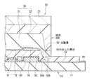
図2は、駆動パネル10,封止パネル20,中間層30および被覆層50の平面的な位置関係を表すものである。駆動パネル10および封止パネル20は必ずしも同じ大きさである必要はなく、例えば、駆動用基板11の一部は、封止パネル20および中間層30により覆われておらず、露出している。この露出した部分には、例えばチタン(Ti)―アルミニウム(Al)合金よりなる端子部80が設けられている。
FIG. 2 illustrates a planar positional relationship among the driving
中間層30は、図2に示したように、封止パネル20の全面に形成されている。また、被覆層50の形成範囲は、中間層30の形成された領域よりも内側の領域(図2の斜線を施した領域)となっている。
The
この表示装置では、例えば、第1電極12と第2電極15との間に所定の電圧が印加されると、有機層14の発光層に電流が注入され、正孔と電子とが再結合することにより発光が起こる。この光は、封止パネル20の側から取り出される。ここでは、中間層30、すなわち、保護膜31および接着層32によって被覆層50の表面50Aだけでなく、その端面50Bが覆われている。したがって、被覆層50の端面50Bが駆動パネル10と封止パネル20との間から外部に露出せず、外部の水分が被覆層50を経路として内部に侵入することが防止され、有機発光素子10R,10G,10Bの劣化が防止される。
In this display device, for example, when a predetermined voltage is applied between the
この表示装置は、例えば、次のようにして製造することができる。 This display device can be manufactured, for example, as follows.
図3ないし図6はこの表示装置の製造方法を工程順に表すものである。まず、図3に示したように、例えば、上述した材料よりなる駆動用基板11に、TFT41,層間絶縁膜42および配線43を有する駆動素子層40と、周辺回路部60とを形成する。
3 to 6 show a method of manufacturing the display device in the order of steps. First, as shown in FIG. 3, for example, a
次に、図4に示したように、駆動用基板11の全面に、感光性を有する材料よりなる感光性膜91を形成する。感光性膜91の構成材料としては、例えば被覆層50の材料として上述した材料を用いることができる。
Next, as shown in FIG. 4, a
続いて、図5に示したように、感光性膜91を露光および現像することにより、駆動素子層40および周辺回路部60を覆う被覆層50を形成する。同時に接続孔51も形成することが可能である。
Subsequently, as shown in FIG. 5, by exposing and developing the
そののち、図6に示したように、有機発光素子10R,10G,10Bおよび端子部80(図1参照)を形成する。すなわち、まず、被覆層50の接続孔51に対応して、上述した材料よりなる第1電極12を形成し、駆動素子層40と第1電極12との電気的導通をとる。次いで、この第1電極12の上に、絶縁層13を所定のパターンで形成する。続いて、絶縁層13の上に補助配線70の支線70Aを形成すると共に、駆動用基板11の周辺部分には補助配線70を形成する。次に、上述した材料よりなる正孔注入層,正孔輸送層,発光層および電子輸送層を順次成膜して有機層14を形成したのち、上述した材料よりなる第2電極15を形成する。
After that, as shown in FIG. 6, the organic
有機発光素子10R,10G,10Bを形成したのち、図7に示したように、保護膜31を、有機発光素子10R,10G,10B並びに被覆層50の表面50Aおよび端面50Bを覆うように形成する。続いて、上述した材料よりなる接着層32を形成する。これにより、中間層30が形成される。
After forming the organic
次に、上述した材料よりなり、必要に応じてカラーフィルタなどを形成した封止用基板21を有する封止パネル20を用意し、駆動パネル10および保護膜31と封止パネル20とを接着層32を介して全面にわたって貼り合わせる。以上により、図1および図2に示した表示装置が完成する。
Next, a sealing
また、この表示装置は、例えば、次のようにして製造することもできる。 This display device can be manufactured, for example, as follows.
まず、図3に示した工程により、駆動用基板11に、駆動素子層40および周辺回路部60を形成する。
First, the
次いで、図8に示したように、被覆層50が形成される領域(図2の斜線を施した領域)と同等のサイズを有するシート状平坦化膜92を用意する。このシート状平坦化膜92を、駆動素子層40および周辺回路部60が形成された駆動用基板11の所定の位置に配置する。これにより、図9に示したように、被覆層50を形成する。
Next, as shown in FIG. 8, a sheet-shaped
続いて、図5に示した工程により、被覆層50に接続孔51を形成する。そののち、図6に示した工程により、有機発光素子10R,10G,10Bおよび端子部80を形成する。続いて、図7に示した工程により、保護膜31および接着層32を順に形成し、接着層32を介して駆動パネル10および保護膜31と封止パネル20とを全面にわたって貼り合わせる。以上により、図1および図2に示した表示装置が完成する。
Subsequently, a
このように本実施の形態では、駆動パネル10と封止パネル20との間の中間層30が、有機発光素子10R,10G,10Bおよび被覆層50の表面50Aだけでなく、更に、被覆層50の端面50Bをも覆うように構成したので、被覆層50の端面50Bが駆動パネル10と封止パネル20との間から外部に露出することがなくなる。従って、外部の水分が被覆層50を経路として内部に侵入し、有機発光素子10R,10G,10Bを劣化させることがなくなり、これにより表示装置の信頼性が向上する。
As described above, in the present embodiment, the
特に、本実施の形態では、保護膜31により有機発光素子10R,10G,10B並びに被覆層50の表面50Aおよび端面50Bを覆い、かつ保護膜31と封止用基板21との間に接着層32を介在させるようにしたので、保護膜31および接着層32によって有機発光素子10R,10G,10Bの劣化を効果的に防止することができる。よって、封止性能を向上させることができ、特に、駆動パネル10と封止パネル20とが接着層32を介して全面にわたって貼り合わせられた完全固体封止構造の表示装置に好適である。
In particular, in the present embodiment, the
なお、本実施の形態では、中間層30が保護膜31および接着層32を有する場合について説明したが、保護膜31は必ずしも設けなくてもよい。例えば、図10に示したように、中間層30が保護膜31を含まず、接着層32のみを含むようにしてもよい。
In this embodiment, the case where the
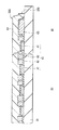
(変形例)
図11は、上記実施の形態の変形例に係る表示装置の断面構造を表すものである。この表示装置は上記実施の形態と同様に、駆動パネル10と封止パネル20との間に中間層30が設けられ、中間層30が被覆層50の表面50Aだけでなく端面50Bをも覆うように構成されたものである。よって、対応する構成要素には同一の符号を付して説明する。
(Modification)
FIG. 11 illustrates a cross-sectional structure of a display device according to a modification of the above embodiment. In this display device, similarly to the above-described embodiment, an
被覆層50は、中間層30の端面30Aからはみ出した部分52を有しており、はみ出した部分52と被覆層50の他の部分とは分離溝53により離間している。これにより、この表示装置では、外部の水分がはみ出した部分52を経路として内部に侵入することがなく、有機発光素子10R,10G,10Bの劣化が防止されるようになっている。
The
この表示装置は、上記実施の形態と同様にして製造することができる。また、この表示装置の作用は上記実施の形態と同様である。 This display device can be manufactured in the same manner as in the above embodiment. The operation of this display device is the same as in the above embodiment.
このように本変形例では、被覆層50に、中間層30の端面30Aからはみ出した部分52を設け、はみ出した部分52と被覆層50の他の部分とを分離溝53により離間するようにしたので、外部の水分がはみ出した部分52を経路として内部に侵入することがなく、有機発光素子10R,10G,10Bの劣化を防止することができる。
As described above, in the present modified example, the
以上、実施の形態を挙げて本発明を説明したが、本発明は上記実施の形態に限定されるものではなく、種々変形が可能である。例えば、上記実施の形態において説明した各層の材料および厚み、または成膜方法および成膜条件などは限定されるものではなく、他の材料および厚みとしてもよく、または他の成膜方法および成膜条件としてもよい。例えば、上記実施の形態においては、駆動用基板11に、第1電極12,絶縁層13,有機層14および第2電極15を駆動用基板11の側から順に積層し、封止パネル20の側から光を取り出すようにした場合について説明したが、積層順序を逆にして、駆動用基板11の上に、第2電極15,有機層14および第1電極12を駆動用基板11の側から順に積層し、駆動用基板11の側から光を取り出すようにすることもできる。
As described above, the present invention has been described with reference to the embodiment. However, the present invention is not limited to the above embodiment, and various modifications are possible. For example, the material and thickness of each layer described in the above embodiment, or the film forming method and film forming conditions are not limited, and may be other materials and thicknesses, or may be other film forming methods and film forming methods. It may be a condition. For example, in the above-described embodiment, the
更に、例えば、上記実施の形態では、第1電極12を陽極、第2電極15を陰極とする場合について説明したが、陽極および陰極を逆にして、第1電極12を陰極、第2電極15を陽極としてもよい。さらに、第1電極12を陰極、第2電極15を陽極とすると共に、駆動用基板11の上に、第2電極15,有機層14および第1電極12を駆動用基板11の側から順に積層し、駆動用基板11の側から光を取り出すようにすることもできる。
Further, for example, in the above-described embodiment, the case where the
加えて、上記実施の形態では、有機発光素子10R,10G,10Bの構成を具体的に挙げて説明したが、全ての層を備える必要はなく、また、他の層を更に備えていてもよい。
In addition, in the above-described embodiment, the configurations of the organic
更にまた、上記実施の形態では、第2電極15が半透過性反射層により構成され、第2電極15の電圧降下を抑制するための補助配線70および支線70Aを備えている場合について説明したが、第2電極15は、半透過性反射層と透明電極とが第1電極12の側から順に積層された構造としてもよい。この透明電極は、半透過性反射層の電気抵抗を下げるためのものであり、発光層で発生した光に対して十分な透光性を有する導電性材料により構成されている。透明電極を構成する材料としては、例えば、ITOまたはインジウムと亜鉛(Zn)と酸素とを含む化合物が好ましい。室温で成膜しても良好な導電性を得ることができるからである。
Furthermore, in the above-described embodiment, a case has been described where the
加えてまた、上記実施の形態では、駆動パネル10および保護膜31と封止パネル20とが接着層32を介して全面にわたって貼り合わせられている場合について説明したが、本発明は、例えば、駆動パネル10の周縁部のみに接着層32を形成して金属缶などを接着するようにした場合など、接着層32が駆動パネル10と封止パネル20との間の一部分のみに形成された場合についても適用することができる。
In addition, in the above-described embodiment, the case where the
10…駆動パネル、11…駆動用基板、12…第1電極、13…絶縁層、14…有機層、15…第2電極、20…封止パネル、21…封止用基板、30…中間層、30A…端面、31…保護膜、32…接着層、40…駆動素子層、41…TFT、42…層間絶縁膜、43…配線、50…被覆層、50A…表面、50B…端面、51…接続孔、52…はみ出した部分、53…分離溝、60…周辺回路部、70…補助配線、70A…支線、80…端子部
DESCRIPTION OF
Claims (13)
封止用基板を有し、前記封止用基板が前記駆動パネルの前記発光素子側に対向配置された封止パネルと、
前記駆動パネルと前記封止パネルとの間に前記複数の発光素子を覆うように設けられると共に、前記被覆層の表面および端面を覆う中間層と
を備えたことを特徴とする表示装置。 A driving panel having a plurality of light-emitting elements on a driving substrate via a driving element layer and a coating layer covering the driving element layer;
A sealing panel having a sealing substrate, wherein the sealing substrate is disposed to face the light emitting element side of the drive panel;
A display device provided between the drive panel and the sealing panel so as to cover the plurality of light emitting elements, and an intermediate layer covering a surface and an end surface of the coating layer.
ことを特徴とする請求項1記載の表示装置。 The display device according to claim 1, wherein the covering layer is made of an organic material.
ことを特徴とする請求項1記載の表示装置。 The display device according to claim 1, wherein a peripheral circuit portion is provided in a peripheral portion of the driving substrate, and the covering layer covers the peripheral circuit portion.
前記複数の発光素子並びに前記被覆層の表面および端面を覆う保護膜と、
前記保護膜と前記封止用基板との間に設けられ、前記駆動パネルおよび前記保護膜と前記封止パネルとを全面にわたって貼り合わせる接着層と
を含むことを特徴とする請求項1記載の表示装置。 The intermediate layer,
A protective film covering the surfaces and end faces of the plurality of light emitting elements and the coating layer,
2. The display according to claim 1, further comprising: an adhesive layer provided between the protective film and the sealing substrate, the adhesive layer bonding the drive panel, the protective film, and the sealing panel over the entire surface. 3. apparatus.
ことを特徴とする請求項1記載の表示装置。 The display device according to claim 1, wherein the intermediate layer includes an adhesive layer for bonding the driving panel and the sealing panel over the entire surface.
ことを特徴とする請求項1記載の表示装置。 The light emitting element has a configuration in which a first electrode, an organic layer including a light emitting layer, and a second electrode are sequentially stacked from the drive substrate side, and light generated in the light emitting layer is emitted from the second electrode side. The display device according to claim 1, wherein the display device is an organic light emitting element to be taken out.
ことを特徴とする請求項6記載の表示装置。 The display device according to claim 6, wherein the light emitting element has an auxiliary electrode for suppressing a voltage drop of the second electrode in contact with the coating layer.
ことを特徴とする請求項1記載の表示装置。 The said coating layer has the part which protruded from the end surface of the said intermediate | middle layer, The said protruding part and the other part of the said coating layer were separated by the separation groove. The said Claim. Display device.
前記複数の発光素子並びに前記被覆層の表面および端面を覆う中間層を形成する工程と、
前記中間層を介して、前記駆動パネルの前記発光素子側に、封止用基板を有する封止パネルを対向配置する工程と
を含むことを特徴とする表示装置の製造方法。 Forming a plurality of light-emitting elements on a driving substrate via a driving element layer and a covering layer covering the driving element layer, and forming a driving panel;
Forming an intermediate layer covering the surfaces and end faces of the plurality of light emitting elements and the coating layer,
A step of arranging a sealing panel having a sealing substrate on the light emitting element side of the drive panel via the intermediate layer.
ことを特徴とする請求項9記載の表示装置の製造方法。 The method for manufacturing a display device according to claim 9, wherein the coating layer is formed by disposing a sheet-like coating film.
ことを特徴とする請求項9記載の表示装置の製造方法。 The method for manufacturing a display device according to claim 9, wherein the covering layer is formed by forming a photosensitive film made of a photosensitive material, and then exposing and developing the photosensitive film.
ことを特徴とする請求項9記載の表示装置の製造方法。 As the intermediate layer, a protective film covering end surfaces of the plurality of light emitting elements and the covering layer, and an adhesive layer are sequentially formed, and then the drive panel, the protective film, and the sealing panel are interposed via the adhesive layer. 10. The method for manufacturing a display device according to claim 9, wherein the bonding is performed over the entire surface.
ことを特徴とする請求項9記載の表示装置の製造方法。
The light emitting element has a configuration in which a first electrode, an organic layer including a light emitting layer, and a second electrode are sequentially stacked from the drive substrate side, and light generated in the light emitting layer is emitted from the second electrode side. The method for manufacturing a display device according to claim 9, wherein the organic light-emitting element is a take-out organic light-emitting element.
Priority Applications (7)
| Application Number | Priority Date | Filing Date | Title |
|---|---|---|---|
| JP2004010345A JP4255844B2 (en) | 2003-02-24 | 2004-01-19 | Organic light-emitting display device and method for manufacturing the same |
| KR1020040011856A KR101021591B1 (en) | 2003-02-24 | 2004-02-23 | Display device and manufacturing method thereof |
| US10/787,038 US7034457B2 (en) | 2003-02-24 | 2004-02-24 | Display unit and method of manufacturing the same |
| SG200400846-2A SG135947A1 (en) | 2003-02-24 | 2004-02-24 | Display unit and method of manufacturing the same |
| CNB2004100326498A CN100442534C (en) | 2003-02-24 | 2004-02-24 | Display device and method of manufacturing same |
| TW093104648A TWI311736B (en) | 2003-02-24 | 2004-02-24 | Display unit and method of manufacturing the same |
| US11/318,371 US7169003B2 (en) | 2003-02-24 | 2005-12-23 | Method of manufacturing a display unit |
Applications Claiming Priority (2)
| Application Number | Priority Date | Filing Date | Title |
|---|---|---|---|
| JP2003046318 | 2003-02-24 | ||
| JP2004010345A JP4255844B2 (en) | 2003-02-24 | 2004-01-19 | Organic light-emitting display device and method for manufacturing the same |
Related Child Applications (1)
| Application Number | Title | Priority Date | Filing Date |
|---|---|---|---|
| JP2007172506A Division JP2007280964A (en) | 2003-02-24 | 2007-06-29 | Organic light-emitting display device and method for manufacturing the same |
Publications (2)
| Publication Number | Publication Date |
|---|---|
| JP2004281380A true JP2004281380A (en) | 2004-10-07 |
| JP4255844B2 JP4255844B2 (en) | 2009-04-15 |
Family
ID=33301688
Family Applications (1)
| Application Number | Title | Priority Date | Filing Date |
|---|---|---|---|
| JP2004010345A Expired - Lifetime JP4255844B2 (en) | 2003-02-24 | 2004-01-19 | Organic light-emitting display device and method for manufacturing the same |
Country Status (6)
| Country | Link |
|---|---|
| US (2) | US7034457B2 (en) |
| JP (1) | JP4255844B2 (en) |
| KR (1) | KR101021591B1 (en) |
| CN (1) | CN100442534C (en) |
| SG (1) | SG135947A1 (en) |
| TW (1) | TWI311736B (en) |
Cited By (10)
| Publication number | Priority date | Publication date | Assignee | Title |
|---|---|---|---|---|
| JP2006269405A (en) * | 2005-03-21 | 2006-10-05 | Samsung Sdi Co Ltd | Light emitting display device and manufacturing method thereof |
| JP2007080717A (en) * | 2005-09-15 | 2007-03-29 | Seiko Epson Corp | Electro-optical device and electronic apparatus |
| JP2007086667A (en) * | 2005-09-26 | 2007-04-05 | Mitsubishi Electric Corp | Display device and large screen display device |
| JPWO2006126304A1 (en) * | 2005-05-25 | 2008-12-25 | シャープ株式会社 | Light emitting circuit board and light emitting display device |
| JP2009522593A (en) * | 2005-12-30 | 2009-06-11 | エルジー・ケム・リミテッド | Flexible display device and manufacturing method thereof |
| WO2013118508A1 (en) * | 2012-02-07 | 2013-08-15 | パナソニック株式会社 | Composite substrate, method for manufacturing same, and organic electroluminescence device |
| US8514158B2 (en) | 2006-03-14 | 2013-08-20 | Nlt Technologies, Ltd. | Liquid crystal driving device |
| JP2013165007A (en) * | 2012-02-13 | 2013-08-22 | Panasonic Corp | Organic electroluminescent element and manufacturing method of the same |
| JP2013186984A (en) * | 2012-03-07 | 2013-09-19 | Panasonic Corp | Composite substrate structure, manufacturing method of the same, and organic electroluminescent element |
| WO2014057647A1 (en) * | 2012-10-11 | 2014-04-17 | パナソニック株式会社 | Organic electroluminescence element and lighting device |
Families Citing this family (24)
| Publication number | Priority date | Publication date | Assignee | Title |
|---|---|---|---|---|
| US7936338B2 (en) | 2002-10-01 | 2011-05-03 | Sony Corporation | Display unit and its manufacturing method |
| KR100552972B1 (en) | 2003-10-09 | 2006-02-15 | 삼성에스디아이 주식회사 | Flat panel display and manufacturing method |
| JP2006113376A (en) * | 2004-10-15 | 2006-04-27 | Toshiba Matsushita Display Technology Co Ltd | Organic EL display device and array substrate |
| KR20060104531A (en) * | 2005-03-30 | 2006-10-09 | 삼성에스디아이 주식회사 | Manufacturing method of light emitting display device |
| JP4611829B2 (en) | 2005-07-19 | 2011-01-12 | 東北パイオニア株式会社 | Method for manufacturing self-luminous panel and self-luminous panel |
| US7722929B2 (en) * | 2005-08-18 | 2010-05-25 | Corning Incorporated | Sealing technique for decreasing the time it takes to hermetically seal a device and the resulting hermetically sealed device |
| US7829147B2 (en) * | 2005-08-18 | 2010-11-09 | Corning Incorporated | Hermetically sealing a device without a heat treating step and the resulting hermetically sealed device |
| US20070040501A1 (en) * | 2005-08-18 | 2007-02-22 | Aitken Bruce G | Method for inhibiting oxygen and moisture degradation of a device and the resulting device |
| US20070145895A1 (en) * | 2005-10-14 | 2007-06-28 | Matsushita Electric Industrial Co., Ltd. | Light emitting apparatus, exposure apparatus, and method for manufacturing light emitting apparatus |
| KR101294844B1 (en) * | 2005-12-29 | 2013-08-08 | 엘지디스플레이 주식회사 | Fabricating method for organic electro-luminescence display device and organic electro-luminescence display device using the same |
| CN101506862B (en) | 2006-06-19 | 2012-12-12 | 索尼株式会社 | Light emitting display device and manufacturing method thereof |
| US20080150421A1 (en) * | 2006-12-21 | 2008-06-26 | Canon Kabushiki Kaisha | Organic light-emitting apparatus |
| JP5007598B2 (en) * | 2007-04-12 | 2012-08-22 | ソニー株式会社 | Display device and manufacturing method thereof |
| JP4424381B2 (en) * | 2007-06-13 | 2010-03-03 | ソニー株式会社 | Display device |
| JP4752818B2 (en) | 2007-07-06 | 2011-08-17 | ソニー株式会社 | Organic EL display device, electronic device, substrate for organic EL display device, and method for manufacturing organic EL display device |
| US7890805B2 (en) * | 2008-12-03 | 2011-02-15 | Ricoh Company, Ltd | Regression testing of a printing system |
| TWI470849B (en) * | 2012-01-20 | 2015-01-21 | Ind Tech Res Inst | Light-emitting element |
| JP5726804B2 (en) * | 2012-04-19 | 2015-06-03 | 株式会社東芝 | Display panel and display device |
| JP6060530B2 (en) * | 2012-06-12 | 2017-01-18 | ソニー株式会社 | Organic electroluminescent device and display device |
| US9159700B2 (en) | 2012-12-10 | 2015-10-13 | LuxVue Technology Corporation | Active matrix emissive micro LED display |
| US9178123B2 (en) | 2012-12-10 | 2015-11-03 | LuxVue Technology Corporation | Light emitting device reflective bank structure |
| US9029880B2 (en) * | 2012-12-10 | 2015-05-12 | LuxVue Technology Corporation | Active matrix display panel with ground tie lines |
| CN104699300B (en) * | 2015-03-05 | 2018-07-06 | 业成光电(深圳)有限公司 | Board structure |
| KR102545253B1 (en) | 2015-05-28 | 2023-06-19 | 엘지디스플레이 주식회사 | Organic light emitting display device and method of manufacturing the same |
Citations (7)
| Publication number | Priority date | Publication date | Assignee | Title |
|---|---|---|---|---|
| JP2001093661A (en) * | 1999-09-22 | 2001-04-06 | Semiconductor Energy Lab Co Ltd | EL display device and electronic device |
| JP2001094113A (en) * | 1998-11-17 | 2001-04-06 | Semiconductor Energy Lab Co Ltd | Semiconductor device and manufacturing method therefor |
| JP2002149112A (en) * | 1999-11-30 | 2002-05-24 | Semiconductor Energy Lab Co Ltd | Electronic device |
| JP2002170668A (en) * | 2000-12-01 | 2002-06-14 | Toppan Printing Co Ltd | Method for manufacturing organic electroluminescent display element |
| JP2002372928A (en) * | 2001-06-13 | 2002-12-26 | Sony Corp | Tiling type display device and manufacturing method thereof |
| JP2003022035A (en) * | 2001-07-10 | 2003-01-24 | Sharp Corp | Organic EL panel and manufacturing method thereof |
| JP2003031363A (en) * | 2001-07-16 | 2003-01-31 | Sharp Corp | Sputtering apparatus, method of manufacturing organic EL element panel using the same, and organic EL element |
Family Cites Families (15)
| Publication number | Priority date | Publication date | Assignee | Title |
|---|---|---|---|---|
| JP3290375B2 (en) * | 1997-05-12 | 2002-06-10 | 松下電器産業株式会社 | Organic electroluminescent device |
| JP3354444B2 (en) * | 1997-07-16 | 2002-12-09 | 三洋電機株式会社 | Organic electroluminescence device |
| JP2001102168A (en) | 1999-09-29 | 2001-04-13 | Sanyo Electric Co Ltd | Display device |
| JP3423261B2 (en) | 1999-09-29 | 2003-07-07 | 三洋電機株式会社 | Display device |
| JP2001102165A (en) | 1999-10-01 | 2001-04-13 | Sanyo Electric Co Ltd | EL display device |
| TW587239B (en) * | 1999-11-30 | 2004-05-11 | Semiconductor Energy Lab | Electric device |
| JP3806596B2 (en) * | 1999-12-27 | 2006-08-09 | 三洋電機株式会社 | Display device and manufacturing method thereof |
| JP4434411B2 (en) * | 2000-02-16 | 2010-03-17 | 出光興産株式会社 | Active drive type organic EL light emitting device and manufacturing method thereof |
| JP2002182380A (en) | 2000-12-14 | 2002-06-26 | Jsr Corp | Radiation-sensitive resin composition for forming insulating film of organic EL display element, insulating film formed therefrom, and organic EL display element |
| US6537688B2 (en) * | 2000-12-01 | 2003-03-25 | Universal Display Corporation | Adhesive sealed organic optoelectronic structures |
| JP4801278B2 (en) * | 2001-04-23 | 2011-10-26 | 株式会社半導体エネルギー研究所 | Light emitting device and manufacturing method thereof |
| TW548860B (en) * | 2001-06-20 | 2003-08-21 | Semiconductor Energy Lab | Light emitting device and method of manufacturing the same |
| KR100413450B1 (en) * | 2001-07-20 | 2003-12-31 | 엘지전자 주식회사 | protecting film structure for display device |
| KR100472502B1 (en) * | 2001-12-26 | 2005-03-08 | 삼성에스디아이 주식회사 | Organic electro luminescence display device |
| US7148624B2 (en) * | 2002-05-07 | 2006-12-12 | Osram Opto Semiconductors (Malaysia) Sdn. Bhd | Uniform deposition of organic layer |
-
2004
- 2004-01-19 JP JP2004010345A patent/JP4255844B2/en not_active Expired - Lifetime
- 2004-02-23 KR KR1020040011856A patent/KR101021591B1/en not_active Expired - Lifetime
- 2004-02-24 CN CNB2004100326498A patent/CN100442534C/en not_active Expired - Lifetime
- 2004-02-24 SG SG200400846-2A patent/SG135947A1/en unknown
- 2004-02-24 US US10/787,038 patent/US7034457B2/en not_active Expired - Lifetime
- 2004-02-24 TW TW093104648A patent/TWI311736B/en not_active IP Right Cessation
-
2005
- 2005-12-23 US US11/318,371 patent/US7169003B2/en not_active Expired - Lifetime
Patent Citations (7)
| Publication number | Priority date | Publication date | Assignee | Title |
|---|---|---|---|---|
| JP2001094113A (en) * | 1998-11-17 | 2001-04-06 | Semiconductor Energy Lab Co Ltd | Semiconductor device and manufacturing method therefor |
| JP2001093661A (en) * | 1999-09-22 | 2001-04-06 | Semiconductor Energy Lab Co Ltd | EL display device and electronic device |
| JP2002149112A (en) * | 1999-11-30 | 2002-05-24 | Semiconductor Energy Lab Co Ltd | Electronic device |
| JP2002170668A (en) * | 2000-12-01 | 2002-06-14 | Toppan Printing Co Ltd | Method for manufacturing organic electroluminescent display element |
| JP2002372928A (en) * | 2001-06-13 | 2002-12-26 | Sony Corp | Tiling type display device and manufacturing method thereof |
| JP2003022035A (en) * | 2001-07-10 | 2003-01-24 | Sharp Corp | Organic EL panel and manufacturing method thereof |
| JP2003031363A (en) * | 2001-07-16 | 2003-01-31 | Sharp Corp | Sputtering apparatus, method of manufacturing organic EL element panel using the same, and organic EL element |
Cited By (14)
| Publication number | Priority date | Publication date | Assignee | Title |
|---|---|---|---|---|
| JP2006269405A (en) * | 2005-03-21 | 2006-10-05 | Samsung Sdi Co Ltd | Light emitting display device and manufacturing method thereof |
| JPWO2006126304A1 (en) * | 2005-05-25 | 2008-12-25 | シャープ株式会社 | Light emitting circuit board and light emitting display device |
| JP4916439B2 (en) * | 2005-05-25 | 2012-04-11 | シャープ株式会社 | Light emitting circuit board and light emitting display device |
| JP2007080717A (en) * | 2005-09-15 | 2007-03-29 | Seiko Epson Corp | Electro-optical device and electronic apparatus |
| JP2007086667A (en) * | 2005-09-26 | 2007-04-05 | Mitsubishi Electric Corp | Display device and large screen display device |
| JP2009522593A (en) * | 2005-12-30 | 2009-06-11 | エルジー・ケム・リミテッド | Flexible display device and manufacturing method thereof |
| US8514158B2 (en) | 2006-03-14 | 2013-08-20 | Nlt Technologies, Ltd. | Liquid crystal driving device |
| WO2013118508A1 (en) * | 2012-02-07 | 2013-08-15 | パナソニック株式会社 | Composite substrate, method for manufacturing same, and organic electroluminescence device |
| US9112181B2 (en) | 2012-02-07 | 2015-08-18 | Panasonic Corporation | Composite substrate, manufacturing method of the same and organic electroluminescence device |
| JP2013165007A (en) * | 2012-02-13 | 2013-08-22 | Panasonic Corp | Organic electroluminescent element and manufacturing method of the same |
| JP2013186984A (en) * | 2012-03-07 | 2013-09-19 | Panasonic Corp | Composite substrate structure, manufacturing method of the same, and organic electroluminescent element |
| WO2014057647A1 (en) * | 2012-10-11 | 2014-04-17 | パナソニック株式会社 | Organic electroluminescence element and lighting device |
| JPWO2014057647A1 (en) * | 2012-10-11 | 2016-08-25 | パナソニックIpマネジメント株式会社 | ORGANIC ELECTROLUMINESCENT ELEMENT AND LIGHTING DEVICE |
| US9620740B2 (en) | 2012-10-11 | 2017-04-11 | Panasonic Intellectual Property Management Co., Ltd. | Organic electroluminescence element and lighting device |
Also Published As
| Publication number | Publication date |
|---|---|
| CN1538786A (en) | 2004-10-20 |
| KR101021591B1 (en) | 2011-03-17 |
| SG135947A1 (en) | 2007-10-29 |
| CN100442534C (en) | 2008-12-10 |
| KR20040076214A (en) | 2004-08-31 |
| JP4255844B2 (en) | 2009-04-15 |
| TWI311736B (en) | 2009-07-01 |
| US20060099873A1 (en) | 2006-05-11 |
| US7034457B2 (en) | 2006-04-25 |
| TW200426739A (en) | 2004-12-01 |
| US7169003B2 (en) | 2007-01-30 |
| US20040217704A1 (en) | 2004-11-04 |
Similar Documents
| Publication | Publication Date | Title |
|---|---|---|
| JP4255844B2 (en) | Organic light-emitting display device and method for manufacturing the same | |
| KR100838082B1 (en) | OLED display device and manufacturing method | |
| KR100579184B1 (en) | Organic light emitting display device | |
| US8754404B2 (en) | Organic light emitting diode display | |
| CN103035665B (en) | Display of organic electroluminescence | |
| JP5593676B2 (en) | Display device and manufacturing method of display device | |
| JP4032909B2 (en) | Manufacturing method of organic light emitting display device | |
| JP6399801B2 (en) | Organic electroluminescence display device | |
| JP4864546B2 (en) | Organic EL display device and manufacturing method thereof | |
| JP2010211984A (en) | Organic el device, method for manufacturing the same, and electronic apparatus | |
| CN115715118A (en) | display device | |
| CN111903187B (en) | display device | |
| JP4924329B2 (en) | Method for manufacturing light emitting device | |
| JP4466550B2 (en) | Display device | |
| CN100495720C (en) | Display device | |
| US9536936B2 (en) | Organic light emitting diode display | |
| JP4543336B2 (en) | Manufacturing method of display device | |
| JP2010218719A (en) | Organic el device and electronic equipment | |
| JP2007280964A (en) | Organic light-emitting display device and method for manufacturing the same | |
| CN112714969B (en) | Light emitting device, method of manufacturing light emitting device, and electronic apparatus | |
| WO2022064562A1 (en) | Display device | |
| KR20100067218A (en) | Organic light emitting display device and method for fabricating the same | |
| JP2008010275A (en) | Image display device | |
| CN120239461A (en) | Display Devices | |
| WO2022018846A1 (en) | Display device |
Legal Events
| Date | Code | Title | Description |
|---|---|---|---|
| A131 | Notification of reasons for refusal |
Free format text: JAPANESE INTERMEDIATE CODE: A131 Effective date: 20060704 |
|
| A521 | Request for written amendment filed |
Free format text: JAPANESE INTERMEDIATE CODE: A523 Effective date: 20060904 |
|
| A131 | Notification of reasons for refusal |
Free format text: JAPANESE INTERMEDIATE CODE: A131 Effective date: 20061122 |
|
| A521 | Request for written amendment filed |
Free format text: JAPANESE INTERMEDIATE CODE: A523 Effective date: 20070122 |
|
| A02 | Decision of refusal |
Free format text: JAPANESE INTERMEDIATE CODE: A02 Effective date: 20070502 |
|
| A521 | Request for written amendment filed |
Free format text: JAPANESE INTERMEDIATE CODE: A523 Effective date: 20070629 |
|
| A521 | Request for written amendment filed |
Free format text: JAPANESE INTERMEDIATE CODE: A523 Effective date: 20080808 |
|
| A521 | Request for written amendment filed |
Free format text: JAPANESE INTERMEDIATE CODE: A523 Effective date: 20081117 |
|
| A01 | Written decision to grant a patent or to grant a registration (utility model) |
Free format text: JAPANESE INTERMEDIATE CODE: A01 |
|
| A61 | First payment of annual fees (during grant procedure) |
Free format text: JAPANESE INTERMEDIATE CODE: A61 Effective date: 20090128 |
|
| FPAY | Renewal fee payment (event date is renewal date of database) |
Free format text: PAYMENT UNTIL: 20120206 Year of fee payment: 3 |
|
| R151 | Written notification of patent or utility model registration |
Ref document number: 4255844 Country of ref document: JP Free format text: JAPANESE INTERMEDIATE CODE: R151 |
|
| FPAY | Renewal fee payment (event date is renewal date of database) |
Free format text: PAYMENT UNTIL: 20120206 Year of fee payment: 3 |
|
| FPAY | Renewal fee payment (event date is renewal date of database) |
Free format text: PAYMENT UNTIL: 20120206 Year of fee payment: 3 |
|
| FPAY | Renewal fee payment (event date is renewal date of database) |
Free format text: PAYMENT UNTIL: 20130206 Year of fee payment: 4 |
|
| R250 | Receipt of annual fees |
Free format text: JAPANESE INTERMEDIATE CODE: R250 |
|
| FPAY | Renewal fee payment (event date is renewal date of database) |
Free format text: PAYMENT UNTIL: 20130206 Year of fee payment: 4 |
|
| FPAY | Renewal fee payment (event date is renewal date of database) |
Free format text: PAYMENT UNTIL: 20140206 Year of fee payment: 5 |
|
| R250 | Receipt of annual fees |
Free format text: JAPANESE INTERMEDIATE CODE: R250 |
|
| R250 | Receipt of annual fees |
Free format text: JAPANESE INTERMEDIATE CODE: R250 |
|
| R250 | Receipt of annual fees |
Free format text: JAPANESE INTERMEDIATE CODE: R250 |
|
| S111 | Request for change of ownership or part of ownership |
Free format text: JAPANESE INTERMEDIATE CODE: R313111 |
|
| R350 | Written notification of registration of transfer |
Free format text: JAPANESE INTERMEDIATE CODE: R350 |
|
| R250 | Receipt of annual fees |
Free format text: JAPANESE INTERMEDIATE CODE: R250 |
|
| R250 | Receipt of annual fees |
Free format text: JAPANESE INTERMEDIATE CODE: R250 |
|
| R250 | Receipt of annual fees |
Free format text: JAPANESE INTERMEDIATE CODE: R250 |
|
| R250 | Receipt of annual fees |
Free format text: JAPANESE INTERMEDIATE CODE: R250 |
|
| R250 | Receipt of annual fees |
Free format text: JAPANESE INTERMEDIATE CODE: R250 |
|
| R250 | Receipt of annual fees |
Free format text: JAPANESE INTERMEDIATE CODE: R250 |
|
| R250 | Receipt of annual fees |
Free format text: JAPANESE INTERMEDIATE CODE: R250 |
|
| R250 | Receipt of annual fees |
Free format text: JAPANESE INTERMEDIATE CODE: R250 |
|
| S303 | Written request for registration of pledge or change of pledge |
Free format text: JAPANESE INTERMEDIATE CODE: R316303 |
|
| R350 | Written notification of registration of transfer |
Free format text: JAPANESE INTERMEDIATE CODE: R350 |
|
| S803 | Written request for registration of cancellation of provisional registration |
Free format text: JAPANESE INTERMEDIATE CODE: R316803 |
|
| R350 | Written notification of registration of transfer |
Free format text: JAPANESE INTERMEDIATE CODE: R350 |
|
| EXPY | Cancellation because of completion of term |