JP2004192694A - Semiconductor storage device - Google Patents
Semiconductor storage device Download PDFInfo
- Publication number
- JP2004192694A JP2004192694A JP2002357630A JP2002357630A JP2004192694A JP 2004192694 A JP2004192694 A JP 2004192694A JP 2002357630 A JP2002357630 A JP 2002357630A JP 2002357630 A JP2002357630 A JP 2002357630A JP 2004192694 A JP2004192694 A JP 2004192694A
- Authority
- JP
- Japan
- Prior art keywords
- port
- memory cell
- cell array
- memory
- word lines
- Prior art date
- Legal status (The legal status is an assumption and is not a legal conclusion. Google has not performed a legal analysis and makes no representation as to the accuracy of the status listed.)
- Pending
Links
- 239000004065 semiconductor Substances 0.000 title claims abstract description 81
- 230000015654 memory Effects 0.000 claims abstract description 428
- 238000003491 array Methods 0.000 claims abstract description 17
- 239000011159 matrix material Substances 0.000 claims description 8
- 230000015572 biosynthetic process Effects 0.000 claims description 4
- 238000009792 diffusion process Methods 0.000 description 191
- 229910021420 polycrystalline silicon Inorganic materials 0.000 description 93
- 229920005591 polysilicon Polymers 0.000 description 93
- XAGFODPZIPBFFR-UHFFFAOYSA-N aluminium Chemical compound [Al] XAGFODPZIPBFFR-UHFFFAOYSA-N 0.000 description 79
- 229910052782 aluminium Inorganic materials 0.000 description 79
- 238000010586 diagram Methods 0.000 description 44
- 101001070329 Geobacillus stearothermophilus 50S ribosomal protein L18 Proteins 0.000 description 26
- 101100005916 Arabidopsis thaliana CER3 gene Proteins 0.000 description 16
- 101100390958 Arabidopsis thaliana FLP2 gene Proteins 0.000 description 16
- 101150088221 FLP1 gene Proteins 0.000 description 16
- 101100299619 Mus musculus Ptpn18 gene Proteins 0.000 description 16
- 101100220842 Schizosaccharomyces pombe (strain 972 / ATCC 24843) clp1 gene Proteins 0.000 description 16
- 102100026561 Filamin-A Human genes 0.000 description 14
- 102100026560 Filamin-C Human genes 0.000 description 14
- 101000913549 Homo sapiens Filamin-A Proteins 0.000 description 14
- 101000913557 Homo sapiens Filamin-C Proteins 0.000 description 14
- 230000006870 function Effects 0.000 description 13
- 230000000694 effects Effects 0.000 description 12
- 101000575029 Bacillus subtilis (strain 168) 50S ribosomal protein L11 Proteins 0.000 description 10
- 102100035793 CD83 antigen Human genes 0.000 description 10
- 101000946856 Homo sapiens CD83 antigen Proteins 0.000 description 10
- 238000001514 detection method Methods 0.000 description 7
- 239000012535 impurity Substances 0.000 description 6
- 230000010354 integration Effects 0.000 description 5
- 230000000644 propagated effect Effects 0.000 description 5
- 101001053754 Homo sapiens Type II iodothyronine deiodinase Proteins 0.000 description 4
- 102100024060 Type II iodothyronine deiodinase Human genes 0.000 description 4
- 101100386518 Caenorhabditis elegans dbl-1 gene Proteins 0.000 description 3
- 125000006850 spacer group Chemical group 0.000 description 3
- 230000003213 activating effect Effects 0.000 description 2
- 230000002093 peripheral effect Effects 0.000 description 2
- 230000004044 response Effects 0.000 description 2
- YAWWQIFONIPBKT-HXUWFJFHSA-N 2-[[(2r)-2-butyl-6,7-dichloro-2-cyclopentyl-1-oxo-3h-inden-5-yl]oxy]acetic acid Chemical compound C1([C@@]2(C(C3=C(Cl)C(Cl)=C(OCC(O)=O)C=C3C2)=O)CCCC)CCCC1 YAWWQIFONIPBKT-HXUWFJFHSA-N 0.000 description 1
- 101001053391 Homo sapiens Thyroxine 5-deiodinase Proteins 0.000 description 1
- XUIMIQQOPSSXEZ-UHFFFAOYSA-N Silicon Chemical compound [Si] XUIMIQQOPSSXEZ-UHFFFAOYSA-N 0.000 description 1
- 102100024373 Thyroxine 5-deiodinase Human genes 0.000 description 1
- 229910052710 silicon Inorganic materials 0.000 description 1
- 239000010703 silicon Substances 0.000 description 1
- 230000003068 static effect Effects 0.000 description 1
Images


Classifications
-
- G—PHYSICS
- G11—INFORMATION STORAGE
- G11C—STATIC STORES
- G11C11/00—Digital stores characterised by the use of particular electric or magnetic storage elements; Storage elements therefor
- G11C11/21—Digital stores characterised by the use of particular electric or magnetic storage elements; Storage elements therefor using electric elements
- G11C11/34—Digital stores characterised by the use of particular electric or magnetic storage elements; Storage elements therefor using electric elements using semiconductor devices
- G11C11/40—Digital stores characterised by the use of particular electric or magnetic storage elements; Storage elements therefor using electric elements using semiconductor devices using transistors
- G11C11/41—Digital stores characterised by the use of particular electric or magnetic storage elements; Storage elements therefor using electric elements using semiconductor devices using transistors forming static cells with positive feedback, i.e. cells not needing refreshing or charge regeneration, e.g. bistable multivibrator or Schmitt trigger
- G11C11/413—Auxiliary circuits, e.g. for addressing, decoding, driving, writing, sensing, timing or power reduction
- G11C11/417—Auxiliary circuits, e.g. for addressing, decoding, driving, writing, sensing, timing or power reduction for memory cells of the field-effect type
- G11C11/418—Address circuits
-
- G—PHYSICS
- G11—INFORMATION STORAGE
- G11C—STATIC STORES
- G11C11/00—Digital stores characterised by the use of particular electric or magnetic storage elements; Storage elements therefor
- G11C11/21—Digital stores characterised by the use of particular electric or magnetic storage elements; Storage elements therefor using electric elements
- G11C11/34—Digital stores characterised by the use of particular electric or magnetic storage elements; Storage elements therefor using electric elements using semiconductor devices
- G11C11/40—Digital stores characterised by the use of particular electric or magnetic storage elements; Storage elements therefor using electric elements using semiconductor devices using transistors
- G11C11/41—Digital stores characterised by the use of particular electric or magnetic storage elements; Storage elements therefor using electric elements using semiconductor devices using transistors forming static cells with positive feedback, i.e. cells not needing refreshing or charge regeneration, e.g. bistable multivibrator or Schmitt trigger
- G11C11/413—Auxiliary circuits, e.g. for addressing, decoding, driving, writing, sensing, timing or power reduction
-
- G—PHYSICS
- G11—INFORMATION STORAGE
- G11C—STATIC STORES
- G11C7/00—Arrangements for writing information into, or reading information out from, a digital store
- G11C7/14—Dummy cell management; Sense reference voltage generators
-
- G—PHYSICS
- G11—INFORMATION STORAGE
- G11C—STATIC STORES
- G11C8/00—Arrangements for selecting an address in a digital store
- G11C8/10—Decoders
-
- G—PHYSICS
- G11—INFORMATION STORAGE
- G11C—STATIC STORES
- G11C8/00—Arrangements for selecting an address in a digital store
- G11C8/14—Word line organisation; Word line lay-out
-
- G—PHYSICS
- G11—INFORMATION STORAGE
- G11C—STATIC STORES
- G11C15/00—Digital stores in which information comprising one or more characteristic parts is written into the store and in which information is read-out by searching for one or more of these characteristic parts, i.e. associative or content-addressed stores
- G11C15/04—Digital stores in which information comprising one or more characteristic parts is written into the store and in which information is read-out by searching for one or more of these characteristic parts, i.e. associative or content-addressed stores using semiconductor elements
Landscapes
- Engineering & Computer Science (AREA)
- Microelectronics & Electronic Packaging (AREA)
- Computer Hardware Design (AREA)
- Static Random-Access Memory (AREA)
- Semiconductor Memories (AREA)
Abstract
Description
【0001】
【発明の属する技術分野】
この発明は半導体記憶装置に関し、特にMOSスタティックRAMの複数のメモリセル構造の組合せに関するものである。
【0002】
【従来の技術】
従来、ポート構造等が異なる複数種のメモリセルからなる半導体記憶装置として例えば特許文献1に開示された半導体記憶装置がある。この半導体記憶装置は、3ポート同時アクセス可能な3ポートセル部と、1個のアクセスポートを有する1ポートセル部とを設け、これらを少なくとも1対のビット線に共通に接続することにより実現している。
【0003】
【特許文献1】
特開平6−349275号公報
【0004】
【発明が解決しようとする課題】
一方、コンピュータ分野等において、ビット長単位でアクセスされるデータを数ビット単位で分割し、分割した数ビット単位で個々のデータにアクセスしたい要求がある。また、ある一部のビットは複数のポートからアクセス可能に構成したいという要求もある。
【0005】
しかしながら、上述した特許文献1の半導体記憶装置では、3ポートセル部と1ポートセル部とがビット線を共有するため、双方のポートセル部に同時にアクセスすることが不可能であり、上記要求に応えることができないという問題点があった。
【0006】
この発明は上記問題点を解決するためになされたもので、異なるメモリセルアレイに存在するメモリセルに対して同時にアクセス可能な1チップ構成の半導体記憶装置を得ることを目的とする。
【0007】
【課題を解決するための手段】
この発明に係る請求項1記載の半導体記憶装置は、第1及び第2のメモリセルアレイを有し、前記第1のメモリセルアレイは、複数行に渡って少なくとも一列配置された複数の第1のメモリセルと、前記複数の第1のメモリセルと行単位に接続される複数の第1のワード線とを含み、前記第2のメモリセルアレイは、マトリクス状に配置された複数の第2のメモリセルと、前記複数の第2のメモリセルと行単位に接続される複数の第2のワード線と、前記複数の第2のメモリセルと行単位に接続され、かつ前記複数の第1のメモリセルのいずれとも接続されない複数の第3のワード線と、前記複数の第2のメモリセルと列単位に対応して設けられ、前記複数の第2のワード線のうち選択状態の第2のワード線に接続される第2のメモリセルとアクセス可能となる複数の第1のビット線と、前記複数の第2のメモリセルと列単位に対応して設けられ、前記複数の第3のワード線のうち選択状態の第3のワード線に接続される第2のメモリセルとアクセス可能となる第2のビット線とを含み、前記半導体記憶装置は、第1のアドレス信号基づき、前記複数の第1のワード線のうちのいずれか及び前記複数の第2のワード線のうちのいずれかを同時に選択状態にする第1の行デコーダをさらに備えて構成される。
【0008】
【発明の実施の形態】
<実施の形態1>
(全体構成)
図1はこの発明の実施の形態1である半導体記憶装置の構成を示すブロック図である。
【0009】
同図に示すように、1ポートメモリセルアレイ11(第1のメモリセルアレイ)と2ポートメモリセルアレイ12(第2のメモリセルアレイ)とを1チップ上に混在させてメモリマクロを構成している。すなわち、1ポートメモリセルアレイ11には第1ポート用ワード線WL1(第1のワード線(共通ワード線))が設けられ、2ポートメモリセルアレイ12には第1ポート用ワード線WL1(第2のワード線(共通ワード線))及び第2ポート用ワード線WL2(第3のワード線)が設けられる。
【0010】
制御回路31はアドレス入力バス信号AD1を受け、読み出し制御入力信号RE1及び書き込み制御入力信号WE1のタイミング制御下で、行アドレスを行デコーダ16(第1の行デコーダ)に列アドレスをカラムセレクタ21及び22に供給する。
【0011】
制御回路32はアドレス入力バス信号AD2を受け、読み出し制御入力信号RE2及び書き込み制御入力信号WE2のタイミング制御下で、行アドレスを行デコーダ17(第2の行デコーダ)に列アドレスをカラムセレクタ23に供給する。
【0012】
行デコーダ16は行アドレスに基づき複数の第1ポート用ワード線WL1をいずれかを選択的に活性状態(選択状態)に、行デコーダ17は行アドレスに基づき複数の第2ポート用ワード線WL2のいずれかを選択的に活性状態にする。
【0013】
カラムセレクタ21は制御回路31からの列アドレスに基づき、複数の第1ポート用ビット線対BL1・バーBL1から4ビット相当分選択し、選択した第1ポート用ビット線対BL1・バーBL1を介して1ポートメモリセルアレイ11に対しデータ入出力バス信号DIO11<7:4>の入出力を行う。
【0014】
カラムセレクタ22は制御回路31からの列アドレスに基づき、複数の第1ポート用ビット線対BL21・バーBL21(第1のビット線)から4ビット相当分選択し、選択した第1ポート用ビット線対BL21・バーBL21を介して2ポートメモリセルアレイ12に対しデータ入出力バス信号DIO12<3:0>の入出力を行う。
【0015】
カラムセレクタ23は制御回路32からの列アドレスに基づき、複数の第2ポート用ビット線対BL22・バーBL22(第2のビット線)から4ビット相当分選択し、選択した第2ポート用ビット線対BL22・バーBL22を介して2ポートメモリセルアレイ12に対しデータ入出力バス信号DIO2<3:0>の入出力を行う。
【0016】
なお、これらカラムセレクタ22〜24はセンスアンプ(SA)機能及び書き込み駆動(WD)機能を有している。
【0017】
(メモリセル構成)
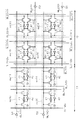
図2は1ポートメモリセルアレイ11及び2ポートメモリセルアレイ12のメモリセルアレイ構造を示す回路図である。なお、同図では説明の都合上、2×2のメモリセルを示しているにすぎず、実際のメモリセルアレイの大きさ(マトリクス状のメモリセル配置)を意味するものではない。
【0018】
1ポートメモリセルアレイ11はメモリセルms00,メモリセルms01,メモリセルms10及びメモリセルms11から構成されている。
【0019】
メモリセルms00〜ms11はそれぞれ、交叉接続されたインバータ41及び42と、インバータ41の入力(インバータ42の出力)に一方電極が接続されたNMOSトランジスタQ11と、インバータ42の入力(インバータ41の出力)に一方電極が接続されたNMOSトランジスタQ12から構成される。
【0020】
第1ポート用ワード線WL1<0>及び線WL1<1>はそれぞれドライバ51及び52(通常、行デコーダ16(図示せず)に内蔵)によって駆動される。
【0021】
同一行のメモリセルms00及びms01において、NMOSトランジスタQ11及びQ12のゲート電極は共通に第1ポート用ワード線WL1<0>に電気的に接続され、同一行のメモリセルms10及びms11において、NMOSトランジスタQ11及びQ12のゲート電極は共通に第1ポート用ワード線WL1<1>に電気的に接続される。
【0022】
同一列のメモリセルms00及びms10は共に第1ポート用ビット線対BL1<0>・バーBL1<0>間に設けられ、これらのメモリセルms00及びms10において、NMOSトランジスタQ11の他方電極が第1ポート用ビット線BL1<0>に電気的に接続され、NMOSトランジスタQ12の他方電極が第1ポート用反転ビット線バーBL1<0>に電気的に接続される。
【0023】
同一列のメモリセルms01及びms11は共に第1ポート用ビット線対BL1<1>・バーBL1<1>間に設けられ、メモリセルms01及びms11において、NMOSトランジスタQ11の他方電極が第1ポート用ビット線BL1<1>に電気的に接続され、NMOSトランジスタQ12の他方電極が第1ポート用反転ビット線バーBL1<1>に電気的に接続される。
【0024】
一方、2ポートメモリセルアレイ12はメモリセルmd00,メモリセルmd01,メモリセルmd10及びメモリセルmd11から構成されている。
【0025】
メモリセルmd00〜md11はそれぞれ、交叉接続されたインバータ41及び42と、インバータ41の入力に一方電極が接続されたNMOSトランジスタQ11及びQ21と、インバータ42の入力に一方電極が接続されたNMOSトランジスタQ12及びQ22とから構成される。
【0026】
第2ポート用ワード線WL2<0>及びWL2<1>はそれぞれドライバ53及び54(通常、行デコーダ17(図示せず)に内蔵)によって駆動される。
【0027】
同一行のメモリセルmd00及びmd01において、NMOSトランジスタQ11及びQ12のゲート電極は共通に第1ポート用ワード線WL1<0>に電気的に接続され、NMOSトランジスタQ21及びQ22のゲート電極は共通に第2ポート用ワード線WL2<0>に電気的に接続される。
【0028】
同一行のメモリセルmd10及びmd11において、NMOSトランジスタQ11及びQ12のゲート電極は共通に第1ポート用ワード線WL1<1>に電気的に接続され、NMOSトランジスタQ21及びQ22のゲート電極は共通に第2ポート用ワード線WL2<1>に電気的に接続される。
【0029】
同一列のメモリセルmd00及びmd10は共に第1ポート用ビット線対BL21<0>・バーBL21<0>間に設けられ、これらのメモリセルmd00及びmd10において、NMOSトランジスタQ11の他方電極が第1ポート用ビット線BL21<0>に電気的に接続され、NMOSトランジスタQ12の他方電極が第1ポート用反転ビット線バーBL21<0>に電気的に接続される。
【0030】
さらに、メモリセルmd00及びmd10は共に第2ポート用ビット線対BL22<0>・バーBL22<0>間に設けられ、これらのメモリセルmd00及びmd10において、NMOSトランジスタQ21の他方電極が第2ポート用ビット線BL22<0>に電気的に接続され、NMOSトランジスタQ22の他方電極が第2ポート用反転ビット線バーBL22<0>に電気的に接続される。
【0031】
同一列のメモリセルmd01及びmd11は共に第1ポート用ビット線対BL21<1>・バーBL21<1>間に設けられ、これらのメモリセルmd01及びmd11において、NMOSトランジスタQ11の他方電極が第1ポート用ビット線BL21<1>に電気的に接続され、NMOSトランジスタQ12の他方電極が第1ポート用反転ビット線バーBL21<1>に電気的に接続される。
【0032】
さらに、メモリセルmd01及びmd11は共に第2ポート用ビット線対BL22<1>・バーBL22<1>間に設けられ、これらのメモリセルmd01及びmd11において、NMOSトランジスタQ21の他方電極が第2ポート用ビット線BL22<1>に電気的に接続され、NMOSトランジスタQ22の他方電極が第2ポート用反転ビット線バーBL22<1>に電気的に接続される。
【0033】
なお、図1及び図2並びに図3以降の図において、記号<>はバス信号(線)であることを意味し、<>内の数字がバス信号名に相当する。また、<n−1:0>は、バス信号0〜バス信号(n−1)のnビット幅の信号を意味する。
【0034】
(動作)
以下、図1及び図2を参照して、第1ポートによる読み出し及び書き込み動作並びに第2ポートによる読み出し及び書き込み動作を説明する。ここで、説明の都合上、1ポートメモリセルアレイ11及び2ポートメモリセルアレイ12のメモリセルアレイ構成をn(行)×m(列)とする。
【0035】
まず、第1ポートの読み出し動作を実行する場合、読み出し制御入力信号RE1をイネーブルにする。読み出し制御入力信号RE1がイネーブル状態になると、アドレス入力バス信号AD1に対応した行アドレスを制御回路31を介して受ける行デコーダ16は、nビットの第1ポート用ワード線WL1<n−1:0>のうちの1つの第1ポート用ワード線WL1<i>(i=0〜n−1のいずれか)を選択的に活性状態にする。
【0036】
すると、活性状態とされた第1ポート用ワード線WL1<i>に接続される1ポートメモリセルアレイ11の選択メモリセルmsi0〜msim及び2ポートメモリセルアレイ12の選択メモリセルmdi0〜mdimそれぞれのNMOSトランジスタQ11及びQ12がオン状態となり、各選択メモリセルの記憶内容が対応の第1ポート用ビット線対BL1・バーBL1及びBL21・バーBL21に伝搬される。
【0037】
そして、アドレス入力バス信号AD1に対応した列アドレスを制御回路31を介して受けるカラムセレクタ21及び22それぞれは、m本の第1ポート用ビット線対BL1・バーBL1及びBL21・バーBL21からそれぞれ4組のビット線対を選択し、内部のセンスアンプによって感知・増幅することにより、データ入出力バス信号DIO11<7:4>及びデータ入出力バス信号DIO12<3:0>を8ビットの読み出しデータとして出力する。
【0038】
次に、第1ポートの書き込み動作を実行する場合、書き込み制御入力信号WE1をイネーブルにする。書き込み制御入力信号WE1がイネーブル状態になると、アドレス入力バス信号AD1に対応した行アドレスを制御回路31を介して受ける行デコーダ16は、nビットの第1ポート用ワード線WL1<n−1:0>のうちの1つの第1ポート用ワード線WL1<i>(i=0〜n−1のいずれか)を選択的に活性状態にする。
【0039】
すると、活性状態とされた第1ポート用ワード線WL1<i>に接続される1ポートメモリセルアレイ11の選択メモリセルmsi0〜msim及び2ポートメモリセルアレイ12の選択メモリセルmdi0〜mdimそれぞれのNMOSトランジスタQ11及びQ12がオン状態となり、各選択メモリセルのインバータ41及び42が第1ポート用ビット線対BL1・バーBL1及びBL21・バーBL21に電気的に接続される。
【0040】
同時に、外部からの書き込みデータを、データ入出力バス信号DIO11<7:4>及びデータ入出力バス信号DIO12<3:0>としてカラムセレクタ21及び22に与える。
【0041】
そして、アドレス入力バス信号AD1に対応した列アドレスを制御回路31を介して受けるカラムセレクタ21及び22それぞれは、m本の第1ポート用ビット線対BL1・バーBL1及びBL21・バーBL21からそれぞれ4組のビット線対を選択し、上記書き込みデータを選択したビット線対に与えることにより、選択したビット線対を“L”または“H”にドライブする。その結果、選択メモリセルに対して上記書き込みデータに基づく書き込みが行える。
【0042】
そして、第2ポートの読み出し動作を実行する場合、読み出し制御入力信号RE2をイネーブルにする。読み出し制御入力信号RE2がイネーブル状態になると、アドレス入力バス信号AD2に対応した行アドレスを制御回路32を介して受ける行デコーダ17は、nビットの第2ポート用ワード線WL2<n−1:0>のうちの1つの第2ポート用ワード線WL2<i>(i=0〜n−1のいずれか)を選択的に活性状態にする。
【0043】
すると、活性状態とされた第2ポート用ワード線WL2<i>に接続される2ポートメモリセルアレイ12の選択メモリセルmdi0〜mdimそれぞれのNMOSトランジスタQ21及びQ22がオン状態となり、各選択メモリセルの記憶内容が対応の第2ポート用ビット線対BL22・バーBL22に伝搬される。
【0044】
そして、アドレス入力バス信号AD2に対応した列アドレスを制御回路32を介して受けるカラムセレクタ23は、m本の第2ポート用ビット線対BL22・バーBL22からそれぞれ4組のビット線対を選択し、内部のセンスアンプによって感知・増幅することにより、データ入出力バス信号DIO2<3:0>を4ビットの読み出しデータとして出力する。
【0045】
次に、第2ポートの書き込み動作を実行する場合、書き込み制御入力信号WE2をイネーブルにする。書き込み制御入力信号WE2がイネーブル状態になると、アドレス入力バス信号AD2に対応した行アドレスを制御回路32を介して受ける行デコーダ17は、nビットの第2ポート用ワード線WL2<n−1:0>のうちの1つの第2ポート用ワード線WL2<i>を選択的に活性状態にする。
【0046】
すると、活性状態とされた第2ポート用ワード線WL2<i>に接続される2ポートメモリセルアレイ12の選択メモリセルmdi0〜mdimそれぞれのNMOSトランジスタQ21及びQ22がオン状態となり、各選択メモリセルのインバータ41及び42が第2ポート用ビット線対BL22・バーBL22に電気的に接続される。
【0047】
同時に、外部からの書き込みデータを、データ入出力バス信号DIO2<3:0>としてカラムセレクタ23に与える。
【0048】
そして、アドレス入力バス信号AD2に対応した列アドレスを制御回路32を介して受けるカラムセレクタ23は、m本の第2ポート用ビット線対BL22・バーBL22から4組のビット線対を選択し、上記書き込みデータを選択したビット線対に与えることにより、選択したビット線対を“L”または“H”にドライブする。その結果、選択メモリセルに対して上記書き込みデータに基づく書き込みが行える。
【0049】
以上説明したように、第1ポートから、1ポートメモリセルアレイ11及び2ポートメモリセルアレイ12に4ビット単位で上位及び下位に分割して保持されている総計8ビットデータの読み書きが可能である。
【0050】
そして、第2ポートから、2ポートメモリセルアレイ12に保持されている下位4ビットデータの読み書きが可能である。この際、上位4ビットデータは全くアクセスされない。
【0051】
その結果、実施の形態1の半導体記憶装置は、8ビット長単位でアクセスされるデータを4ビット単位で分割し、分割した下位4ビット単位のデータにアクセスすることができ、下位4ビットは第1及び第2のポートからアクセス可能にすることにより、データの分割アクセスの要求に応じた読み書きが行える。
【0052】
このように、実施の形態1では、一の行デコーダ16によって互いに回路構成が異なるメモリセルを有する1ポートメモリセルアレイ11及び2ポートメモリセルアレイ12が同時制御可能であるため、異なる構造のシングルポートメモリセル及び2ポートメモリセルに対して同時にアクセス可能な1チップ構成の半導体記憶装置を得ることができる。
【0053】
また、1ポートメモリセルアレイ11を2ポートメモリセルで置き換えて構成しても実施の形態1と等価な動作は可能であるが、この場合と比較すると、上位4ビットを1ポートメモリセルで構成する分面積の縮小が図れ、第2ポートではアクセス不要な上位4ビット分の制御回路及びカラムセレクタ等の削減が図れる分、レイアウト面積の縮小が図れる。このように、回路規模が小さくなることから、動作時及びスタンバイ時の消費電力の低減化を図ることができる。
【0054】
(レイアウト構成)
図3及び図4は1ポートメモリセルアレイ11のシングルポートメモリセルMSのレイアウト構成を示す説明図である。図3は主として第1アルミ配線層下のレイアウト構成を平面視した説明図である。図4は第2アルミ配線層上のレイアウト構成を平面視した説明図である。
【0055】
なお、図2で示したインバータ41はPMOSトランジスタP1及びNMOSトランジスタN1により構成されるCMOSインバータであり、インバータ42はNMOSトランジスタP2及びNMOSトランジスタN2で構成されるCMOSインバータであるとする。
【0056】
図3に示すように、PMOSトランジスタP1,P2はNウエル領域NW内に形成され、NMOSトランジスタN1とNMOSトランジスタQ11とはPウエル領域PW1内に形成され、NMOSトランジスタN2とNMOSトランジスタQ12とはPウエル領域PW0内に形成される。Pウエル領域PW0とPウエル領域PW1とはNウエル領域NWを挟んで各々反対側に形成される。
【0057】
Nウエル領域NW内において、P+拡散領域FLP1上を横断するポリシリコン配線PL1によりPMOSトランジスタP1を構成し、P+拡散領域FLP2上を横断するポリシリコン配線PL2によりPMOSトランジスタP2を構成する。
【0058】
Pウエル領域PW1内において、N+拡散領域FLN1上を横断するポリシリコン配線PL1によりNMOSトランジスタN1を構成し、N+拡散領域FLQ11を横断するポリシリコン配線PL11によってNMOSトランジスタQ11を構成する。なお、ポリシリコン配線PL1はNウエル領域NWからPウエル領域PW1にかけて形成されることにより、NMOSトランジスタN1及びPMOSトランジスタP1のゲートとして共有される。
【0059】
Pウエル領域PW0内において、N+拡散領域FLN2上を横断するポリシリコン配線PL2によりNMOSトランジスタN2を構成し、N+拡散領域FLQ12を横断するポリシリコン配線PL12によってNMOSトランジスタQ12を構成する。なお、ポリシリコン配線PL2はNウエル領域NWからPウエル領域PW0にかけて形成されることにより、NMOSトランジスタN2及びPMOSトランジスタP2のゲートとして共有される。
【0060】
また、ポリシリコン配線PL1及びポリシリコン配線PL12は同一直線上に形成され、ポリシリコン配線PL2及びポリシリコン配線PL11は同一直線上に形成され、拡散領域FLP1,FLN1及びFLQ12が同一直線上にほぼ同一形状で配置され、拡散領域FLP2,FLN2及びFLQ11が同一直線上にほぼ同一形状で配置される。
【0061】
その結果、PMOSトランジスタP1,NMOSトランジスタN1及びNMOSトランジスタQ12を同一直線上に沿って形成でき、PMOSトランジスタP2,NMOSトランジスタN2及びNMOSトランジスタQ11を同一直線上に沿って形成することにより、シングルポートメモリセルMSのセル高さHC1を2トランジスタ相当分に設定することができる。なお、本明細書中において、セル高さとは、レイアウト構成上のビット線形成方向(図中縦方向)の形成長を意味する。
【0062】
上述したP+拡散領域FLP1,FLP2はP型の不純物を注入,拡散することにより得られ、N+拡散領域FLN1,FLN2,FLQ11,FLQ12はN型の不純物を注入,拡散することにより得られる。なお、図3の説明において、各拡散領域はポリシリコン配線に対して、図中上方にある領域を一方領域、下方にある領域を他方領域として説明する。
【0063】
Pウェル領域PW1において、N+拡散領域FLN1の一方領域上のグランド配線LG1(第1層アルミ配線)は拡散コンタクトホールCHを介して拡散領域FLN1と電気的に接続される。ポリシリコン配線PL11はゲートコンタクトホールGCを介して、ワード線1WL1(第1層アルミ配線)に電気的に接続され、拡散領域FLQ11の他方領域上のビット線1BL1(第1層アルミ配線)は拡散コンタクトホールCHを介して拡散領域FLQ11の他方領域と電気的に接続される。
【0064】
なお、拡散コンタクトホールCHは拡散領域と第1層(アルミ)配線とのコンタクトホールを意味し、ゲートコンタクトホールGCはポリシリコン配線と第1層配線とのコンタクトホールを意味する。
【0065】
Nウェル領域NWにおいて、拡散領域FLP1の一方領域上の電源配線LV1(第1層アルミ配線)は拡散コンタクトホールCHを介して拡散領域FLP1の一方領域と電気的に接続され、拡散領域FLP2の他方領域上の電源配線LV1は拡散コンタクトホールCHを介して拡散領域FLP2の他方領域と電気的に接続される。
【0066】
Pウェル領域PW0において、拡散領域FLQ12の一方領域上の反転ビット線バー1BL1(第1層アルミ配線)は拡散コンタクトホールCHを介して拡散領域FLQ1の一方領域と電気的に接続され、ポリシリコン配線PL12上のワード線1WL1はゲートコンタクトホールGCを介してポリシリコン配線PL12と電気的に接続される。拡散領域FLN2の他方領域上のグランド配線LG1は拡散コンタクトホールCHを介して拡散領域FLN2の他方領域と電気的に接続される。
【0067】
拡散領域FLN1の他方領域上からP+拡散領域FLP1の他方領域上に伸びて形成される第1層アルミ配線であるアルミ配線AL11は、拡散領域FLN1の一方領域と拡散コンタクトホールCHを介して電気的に接続される。そして、P+拡散領域FLP1の他方領域からポリシリコン配線PL2にかけて形成されるシェアードコンタクトSCによって、アルミ配線AL11がP+拡散領域FLP1の他方領域及びポリシリコン配線PL2と電気的に接続される。
【0068】
拡散領域FLN2の一方領域上からP+拡散領域FLP2の一方領域上に伸びて形成される第1層アルミ配線であるアルミ配線AL12は、拡散領域FLN2の一方領域と拡散コンタクトホールCHを介して電気的に接続される。そして、P+拡散領域FLP2の一方領域からポリシリコン配線PL1にかけて形成されるシェアードコンタクトSCによって、アルミ配線AL12がP+拡散領域FLP2の一方領域及びポリシリコン配線PL1と電気的に接続される。
【0069】
図4に示すように、グランド配線LG2(第2層アルミ配線)はビアホールVH1を介して下方のグランド配線LG1(図示せず)と電気的に接続される。電源配線LV2(第2層アルミ配線)はビアホールVH1を介して下方の電源配線LV1(図示せず)と電気的に接続される。
【0070】
ワード線2WL1(第2層アルミ配線)はビアホールVH1を介してワード線1WL1(図示せず)と電気的に接続され、ワード線3WL1(第3層アルミ配線)はビアホールVH2を介してワード線2WL1と電気的に接続される。これらワード線1WL1〜ワード線3WL1によって図1及び図2の第1ポート用ワード線WL1を構成する。
【0071】
ワード線3WL1はPウエル領域PW0,PW1及びNウエル領域NWを横断して形成される。なお、ビアホールVH1は第1層配線,第2層(アルミ)配線間の接続用、ビアホールVH2は第2層配線,第3層(アルミ)配線間の接続用のビアホールを意味する。
【0072】
ビット線2BL1(第2層アルミ配線)はビアホールVH1を介して下方のビット線1BL1(図示せず)と電気的に接続され、反転ビット線バー2BL1(第2層アルミ配線)はビアホールVH1を介して下方の反転ビット線バー1BL1(図示せず)と電気的に接続される。
【0073】
ビット線2BL1,ビット線1BL1及び反転ビット線バー2BL1,バー1BL1によって、図1及び図2の第1ポート用ビット線対BL1及びバーBL1を構成する。
【0074】
ビット線2BL1,バー2BL1、グランド配線LG2及び電源配線LV2は、それぞれPウエル領域PW1,PW0及びNウエル領域NW上を図中縦方向に互いに並行して形成される。
【0075】
図5及び図6は2ポートメモリセルアレイ12の2ポートメモリセルMDのレイアウト構成を示す説明図である。図5は主として第1アルミ配線層下のレイアウト構成を平面視した説明図である。図6は第2アルミ配線層上のレイアウト構成を平面視した説明図である。
【0076】
なお、図2で示したインバータ41はPMOSトランジスタP1及びNMOSトランジスタN1により構成されるCMOSインバータであり、インバータ42はNMOSトランジスタP2及びNMOSトランジスタN2で構成されるCMOSインバータであるとする。
【0077】
図5に示すように、PMOSトランジスタP1,P2はNウエル領域NW内に形成され、NMOSトランジスタN1とNMOSトランジスタQ21及びQ22とはPウエル領域PW1内に形成され、NMOSトランジスタN2とNMOSトランジスタQ11及びQ12とはPウエル領域PW0内に形成される。Pウエル領域PW0とPウエル領域PW1とはNウエル領域NWを挟んで各々反対側に形成される。
【0078】
Nウエル領域NW内において、P+拡散領域FLP1上を横断するポリシリコン配線PL1によりPMOSトランジスタP1を構成し、P+拡散領域FLP2上を横断するポリシリコン配線PL2によりPMOSトランジスタP2を構成する。
【0079】
Pウエル領域PW0内において、N+拡散領域FLN1上を横断するポリシリコン配線PL1によりNMOSトランジスタN1を構成し、N+拡散領域FLQ11及びFLQ12を横断するポリシリコン配線PL10によってNMOSトランジスタQ11及びQ12を構成する。なお、ポリシリコン配線PL1はNウエル領域NWからPウエル領域PW1にかけて形成されることにより、NMOSトランジスタN1及びPMOSトランジスタP1のゲートとして共有され、ポリシリコン配線PL10はNMOSトランジスタQ11及びQ12のゲートとして共有される。
【0080】
Pウエル領域PW1内において、N+拡散領域FLN2上を横断するポリシリコン配線PL2によりNMOSトランジスタN2を構成し、N+拡散領域FLQ21及びFLQ22を横断するポリシリコン配線PL20によってNMOSトランジスタQ21及びQ22をそれぞれ構成する。なお、ポリシリコン配線PL2はNウエル領域NWからPウエル領域PW0にかけて形成されることにより、NMOSトランジスタN2及びPMOSトランジスタP2のゲートとして共有され、ポリシリコン配線PL20はNMOSトランジスタQ21及びQ22のゲートして共有される。
【0081】
また、ポリシリコン配線PL1及びポリシリコン配線PL20は同一直線上に形成され、ポリシリコン配線PL2及びポリシリコン配線PL10は同一直線上に形成され、拡散領域FLP1,FLN1,FLQ21及びFLQ22が同一直線上に配置され、拡散領域FLP2,FLN2,FLQ11及びFLQ12が同一直線上に配置される。
【0082】
その結果、PMOSトランジスタP1,NMOSトランジスタN1,Q21,及びQ22を同一直線上に沿って形成でき、PMOSトランジスタP2,NMOSトランジスタN2,Q11及びQ12を同一直線上に沿って形成することにより、2ポートメモリセルMDのセル高さHC2をシングルポートメモリセルMSと同様に2トランジスタ相当分に設定する(HC2=HC1)ことができる。
【0083】
上述したP+拡散領域FLP1,FLP2はP型の不純物を注入,拡散することにより得られ、N+拡散領域FLN1,FLN2,FLQ11,FLQ12,FLQ21及びFLQ22はN型の不純物を注入,拡散することにより得られる。なお、図5の説明において、各拡散領域はポリシリコン配線に対して、図中上方にある領域を一方領域、下方にある領域を他方領域として説明する。
【0084】
Pウェル領域PW0において、N+拡散領域FLN1の一方領域上のグランド配線LG1は拡散コンタクトホールCHを介して拡散領域FLN1の一方領域と電気的に接続される。ポリシリコン配線PL10はゲートコンタクトホールGCを介して、ワード線1WL1に電気的に接続され、拡散領域FLQ11の他方領域上のビット線1BL21(第1層アルミ配線)は拡散コンタクトホールCHを介して拡散領域FLQ11の他方領域と電気的に接続され、拡散領域FLQ12の他方領域上の反転ビット線バー1BL21(第1層アルミ配線)は拡散コンタクトホールCHを介して拡散領域FLQ12の他方領域と電気的に接続される。
【0085】
さらに、N+拡散領域FLQ11の一方領域からポリシリコン配線PL1にかけて形成されるシェアードコンタクトSCによって、ポリシリコン配線PL1とN+拡散領域FLQ12の一方領域とが電気的に接続される。
【0086】
Nウェル領域NWにおいて、拡散領域FLP1の一方領域上の電源配線LV1は拡散コンタクトホールCHを介して拡散領域FLP1の一方領域と電気的に接続され、拡散領域FLP2の他方領域上の電源配線LV1は拡散コンタクトホールCHを介して拡散領域FLP2の他方領域と電気的に接続される。
【0087】
Pウェル領域PW1において、拡散領域FLQ21の一方領域上のビット線1BL22(第1層アルミ配線)は拡散コンタクトホールCHを介して拡散領域FLQ21の一方領域と電気的に接続され、拡散領域FLQ22の一方領域上の反転ビット線バー1BL22(第1層アルミ配線)は拡散コンタクトホールCHを介して拡散領域FLQ22の一方領域と電気的に接続される。
【0088】
ポリシリコン配線PL20上のワード線1WL2(第1層アルミ配線)はゲートコンタクトホールGCを介してポリシリコン配線PL20と電気的に接続され、拡散領域FLN2の他方領域上のグランド配線LG1は拡散コンタクトホールCHを介して拡散領域FLN2の他方領域と電気的に接続される。
【0089】
拡散領域FLN1の他方領域上からP+拡散領域FLP1の他方領域上に伸びて形成される第1層アルミ配線であるアルミ配線AL11は、拡散領域FLN1の一方領域と拡散コンタクトホールCHを介して電気的に接続される。そして、P+拡散領域FLP1の他方領域からポリシリコン配線PL2にかけて形成されるシェアードコンタクトSCによって、アルミ配線AL11がP+拡散領域FLP1の他方領域及びポリシリコン配線PL2と電気的に接続される。
【0090】
拡散領域FLN2の一方領域上からP+拡散領域FLP2の一方領域上に伸びて形成される第1層アルミ配線であるアルミ配線AL12は、拡散領域FLN2の一方領域と拡散コンタクトホールCHを介して電気的に接続される。そして、P+拡散領域FLP2の一方領域からポリシリコン配線PL1にかけて形成されるシェアードコンタクトSCによって、アルミ配線AL12がP+拡散領域FLP2の一方領域及びポリシリコン配線PL1と電気的に接続される。
【0091】
図6に示すように、グランド配線LG2はビアホールVH1を介して下方のグランド配線LG1(図示せず)と電気的に接続される。電源配線LV2はビアホールVH1を介して下方の電源配線LV1(図示せず)と電気的に接続される。
【0092】
ワード線2WL1はビアホールVH1を介してワード線1WL1(図示せず)と電気的に接続され、ワード線3WL1はビアホールVH2を介してワード線2WL1と電気的に接続される。これらワード線1WL1〜ワード線3WL1によって図1及び図2の第1ポート用ワード線WL1を構成する。
【0093】
ワード線2WL2(第2層アルミ配線)はビアホールVH1を介してワード線1WL2(図示せず)と電気的に接続され、ワード線3WL2(第3層アルミ配線)はビアホールVH2を介してワード線2WL2と電気的に接続される。これらワード線1WL2〜ワード線3WL2によって図1及び図2の第2ポート用ワード線WL2を構成する。
【0094】
ワード線3WL1及び3WL2は、Pウエル領域PW0,PW1及びNウエル領域NWを横断して形成される。
【0095】
ビット線2BL21(第2層アルミ配線)はビアホールVH1を介して下方のビット線1BL21(図示せず)と電気的に接続され、反転ビット線バー2BL21(第2層アルミ配線)はビアホールVH1を介して下方の反転ビット線バー1BL21(図示せず)と電気的に接続される。
【0096】
ビット線2BL22(第2層アルミ配線)はビアホールVH1を介して下方のビット線1BL22(図示せず)と電気的に接続され、反転ビット線バー2BL22(第2層アルミ配線)はビアホールVH1を介して下方の反転ビット線バー1BL22(図示せず)と電気的に接続される。
【0097】
ビット線2BL21,ビット線1BL21及び反転ビット線バー2BL21,バー1BL21によって、図1及び図2の第1ポート用ビット線対BL21及びバーBL21を構成し、ビット線2BL22,ビット線1BL22及び反転ビット線バー2BL22,バー1BL22によって、図1及び図2の第2ポート用ビット線対BL22及びバーBL22を構成する。
【0098】
ビット線2BL21,バー2BL21、ビット線2BL22,バー2BL22、グランド配線LG2及び電源配線LV2は、それぞれPウエル領域PW1,PW0及びNウエル領域NW上を図中縦方向に互いに並行して形成される。
【0099】
図7は1ポートメモリセルアレイ11及び2ポートメモリセルアレイ12の境界近傍におけるシングルポートメモリセルMS及び2ポートメモリセルMDのレイアウト構成を示す説明図である。なお、図7は主として第1アルミ配線層下のレイアウト構成を平面視した説明図である。
【0100】
同図に示すように、シングルポートメモリセルMS及び2ポートメモリセルMDのセル高さを同一(HC1=HC2)に設定することにより、スペーサー等の無駄な領域を設けることなく、シングルポートメモリセルMS及び2ポートメモリセルMDを隣接配置することができる。この際、図7に示すように、境界線39上にあるワード線1WL1及びゲートコンタクトホールGC及びビアホールVH1(図示せず)を共有させている。
【0101】
<実施の形態2>
図8はこの発明に実施の形態2である半導体記憶装置の構成を示すブロック図である。実施の形態2の半導体記憶装置は、1ポートメモリセル構成のメモリマクロ60(第1のメモリセルアレイ)と2ポートメモリセル構成のメモリマクロ70(第2のメモリセルアレイ)とを用いて、1チップの半導体記憶装置を実現している。
【0102】
同図に示すように、独立して設けられたメモリマクロ60及び70の組合せにより実現している。メモリマクロ60は1ポートメモリセルアレイ61、行デコーダ62、制御回路63及びカラムセレクタ64から構成される。1ポートメモリセルアレイ61には第1ポート用ワード線WL1(第1のワード線)が設けられ、2ポートメモリセルアレイ71には第1ポート用ワード線WL21(第2のワード線)及び第2ポート用ワード線WL22(第3のワード線)が設けられる。
【0103】
制御回路63はアドレス入力バス信号AD1を受け、読み出し制御入力信号RE1及び書き込み制御入力信号WE1のタイミング制御下で、行アドレスを行デコーダ62に列アドレスをカラムセレクタ64に供給する。行デコーダ62(第1の行デコーダ(その1))は行アドレスに基づき複数の第1ポート用ワード線WL1のいずれかを選択的に活性状態する。
【0104】
カラムセレクタ64は制御回路63からの列アドレスに基づき、複数の第1ポート用ビット線対BL1・バーBL1から4ビット相当分選択し、選択した第1ポート用ビット線対BL1・バーBL1を介して1ポートメモリセルアレイ61に対しデータ入出力バス信号DIO11<7:4>の入出力を行う。
【0105】
一方、メモリマクロ70は2ポートメモリセルアレイ71、第1ポート用の周辺回路(行デコーダ72(第1の行デコーダ(その2))、制御回路73及びカラムセレクタ74)及び第2ポート用の周辺回路(行デコーダ75(第2の行デコーダ)、制御回路76及びカラムセレクタ77)から構成される。
【0106】
制御回路73はアドレス入力バス信号AD1を受け、読み出し制御入力信号RE1及び書き込み制御入力信号WE1のタイミング制御下で、行アドレスを行デコーダ72に列アドレスをカラムセレクタ74に供給する。行デコーダ72は行アドレスに基づき複数の第1ポート用ワード線WL21のいずれかを選択的に活性状態にする。
【0107】
カラムセレクタ74は制御回路73からの列アドレスに基づき、複数の第1ポート用ビット線対BL21・バーBL21から4ビット相当分選択し、選択した第1ポート用ビット線対BL21・バーBL21を介して2ポートメモリセルアレイ71に対しデータ入出力バス信号DIO11<3:0>の入出力を行う。
【0108】
制御回路76はアドレス入力バス信号AD2を受け、読み出し制御入力信号RE2及び書き込み制御入力信号WE2のタイミング制御下で、行アドレスを行デコーダ75に列アドレスをカラムセレクタ77に供給する。行デコーダ75は行アドレスに基づき複数の第2ポート用ワード線WL22のいずれかを選択的に活性状態にする。
【0109】
カラムセレクタ77は制御回路76からの列アドレスに基づき、複数の第2ポート用ビット線対BL22・バーBL22から4ビット相当分選択し、選択した第2ポート用ビット線対BL22・バーBL22を介して2ポートメモリセルアレイ71に対しデータ入出力バス信号DIO2<3:0>の入出力を行う。
【0110】
なお、これらカラムセレクタ64,74及び77はセンスアンプ機能及び書き込み駆動機能を有している。
【0111】
なお、実施の形態2の半導体記憶装置の動作は、実施の形態1の一の行デコーダ16による1ポートメモリセルアレイ11及び2ポートメモリセルアレイ12の同時制御が、2つの行デコーダ62及び72による1ポートメモリセルアレイ61及び2ポートメモリセルアレイ71の同時制御に置き換わる点を除いて、基本的に実施の形態1の動作と同様に行われる。
【0112】
したがって、実施の形態2の半導体記憶装置は、1ポートメモリセルアレイ61及び2ポートメモリセルアレイ71において4ビット単位で上位及び下位に分割して保持されている総計8ビットデータの読み書きが、アドレス入力バス信号AD1に基づき第1ポートから可能である。
【0113】
そして、2ポートメモリセルアレイ71に保持されている下位4ビットデータの読み書きが、アドレス入力バス信号AD2に基づき第2ポートから可能である。この際、上位4ビットデータは全くアクセスされない。
【0114】
その結果、実施の形態2の半導体記憶装置は、8ビット長単位でアクセスされるデータを4ビット単位で分割し、分割した下位4ビット単位のデータにアクセスすることができ、下位4ビットは第1及び第2のポートからアクセス可能にすることにより、データの分割アクセスの要求に応じた読み書きが行える。
【0115】
このように、実施の形態2では、メモリマクロ60及びメモリマクロ70を組み合わせ、異なるポート構成の1ポートメモリセルアレイ61及び2ポートメモリセルアレイ71それぞれが、同一のアドレス入力バス信号AD1に基づく行デコーダ62及び63によって同時制御が可能であるため、1ポートメモリセルアレイ61及び2ポートメモリセルアレイ71に対して同時にアクセス可能な1チップ構成の半導体記憶装置を得ることができる。
【0116】
実施の形態2の半導体記憶装置は、実施の形態1の半導体記憶装置と比較した場合、1ポートメモリセルアレイ61及び2ポートメモリセルアレイ71の第1ポート用ワード線WL1及びWL21を行デコーダ62及び72によって個別に駆動する分、ワード線の抵抗成分による信号伝搬遅延の増大を抑制することができる効果を奏する。
【0117】
さらに、実施の形態2の行デコーダ62及び72から1ポートメモリセルアレイ61及び2ポートメモリセルアレイ71それぞれ最も遠い位置あるメモリセルまでの距離を、実施の形態1の行デコーダ16から最も遠い位置あるメモリセルまでの距離よりも短くできる分、ワード線の抵抗成分による信号伝搬遅延の増大を抑制することができる効果を奏する。
【0118】
一方、図1で示した実施の形態1の構成は、図8で示した構成とを比較すると、行デコーダ及び制御回路数を1つ削減(図1では共に2個、図8では共に3個)できており、より集積度の向上が図れている。
【0119】
<実施の形態3>
図9はこの発明の実施の形態3である半導体記憶装置の構成を示すブロック図である。
【0120】
同図に示すように、行デコーダ18(第1の行デコーダ)を間に挟みながら1ポートメモリセルアレイ11L(第1のメモリセルアレイ)と2ポートメモリセルアレイ12R(第2のメモリセルアレイ)とを1チップ上に混在させてメモリマクロを構成している。1ポートメモリセルアレイ11Lには第1ポート用ワード線WL1L(第1のワード線)が設けられ、2ポートメモリセルアレイ12Rには第1ポート用ワード線WL1R(第2のワード線)及び第2ポート用ワード線WL2(第3のワード線)が設けられる。
【0121】
行デコーダ18は同一行が共通に活性状態になるように第1ポート用ワード線WL1L及びWL1Rを駆動する。他の構成は図1で示した実施の形態1と同様である。
【0122】
このように、実施の形態3では、1ポートメモリセルアレイ11L及び2ポートメモリセルアレイ12Rに設けられる第1ポート用ワード線WL1L及びWL1Rの活性状態にする制御を、1ポートメモリセルアレイ11L,2ポートメモリセルアレイ12R間にレイアウト配置される行デコーダ18によって行単位に共通に行っている。
【0123】
図10は図9の行デコーダ18の内部構成を示す説明図である。同図に示すように、行デコーダ18はデコード回路18aを有し、制御回路30を介して得られるアドレス入力バス信号AD1に基づき、最終段論理ゲート群65からの出力線OL<0>〜OL<n−1>のうちいずれかを選択的に“H”レベルにする。
【0124】
出力線OL<0>〜OL<n−1>はドライバDRL<0>〜DRL<n−1>の入力部に接続されるとともに、ドライバDRR<0>〜DRR<n−1>の入力部に接続される。そして、ドライバDRL<0>〜DRL<n−1>はWL1L<0>〜WL1L<n−1>を駆動し、ドライバDRR<0>〜DRR<n−1>はWL1R<0>〜WL1R<n−1>を駆動する。したがって、同一行の第1ポート用ワード線WL1L<i>及びWL1R<i>は、共通の出力線OL<i>によって共通に選択(“H”レベルに)される。
【0125】
このような構成の実施の形態3の半導体記憶装置は、実施の形態1の効果に加え、以下の効果をさらに奏する。
【0126】
実施の形態3の半導体記憶装置は、実施の形態1の半導体記憶装置と比較した場合、1ポートメモリセルアレイ11L,2ポートメモリセルアレイ12Rの第1ポート用ワード線WL1L、WL1Rを個別に駆動する分、ワード線の抵抗成分による信号伝搬遅延の増大を抑制することができる第1の効果を奏する。
【0127】
さらに、実施の形態3の行デコーダ18から最も遠い位置あるメモリセルまでの距離を、実施の形態1の行デコーダ16から最も遠い位置あるメモリセルまでの距離よりも短くできる分、ワード線の抵抗成分による信号伝搬遅延の増大を抑制することができる第2の効果を奏する。
【0128】
なお、実施の形態3では、1ポートメモリセルアレイ11L及び2ポートメモリセルアレイ12R用に別々の第1ポート用ワード線WL1L及びWL1Rを設けたが、実施の形態1と同様に、1ポートメモリセルアレイ11L及び2ポートメモリセルアレイ12Rで共用される共通ワード線として、1本の第1ポート用ワード線WL1を行単位に設け、共通のドライバによってドライブする構成によっても、ワード線の抵抗成分による信号伝搬遅延の増大を抑制することができる上記第2の効果を奏することはできる。
【0129】
<実施の形態4>
(全体構成)
図11はこの発明の実施の形態4である半導体記憶装置の構成を示すブロック図である。
【0130】
同図に示すように、1ポートメモリセルアレイ11と連想(CAM:Content Addressable Memory)セルアレイ13(第2のメモリセルアレイ)とを1チップ上に混在させてメモリマクロを構成している。すなわち、1ポートメモリセルアレイ11には第1ポート用ワード線WL1(第1のワード線(共通ワード線))が設けられ、CAMセルアレイ13には第1ポート用ワード線WL1(第2のワード線(共通ワード線))及び第2ポートとしてのマッチ線ML(第3のワード線)が設けられる。
【0131】
行デコーダ16、制御回路31、カラムセレクタ21,22は図1で示した実施の形態1と同様であるため、説明を省略する。
【0132】
制御回路33はアド比較制御入力信号MEのタイミング制御下で、ドライバ回路26及び一致検出回路27の動作を制御する。
【0133】
ドライバ回路26は制御回路33の制御下でデータ比較検索時に、m本のサーチ線対SL・バーSLに相当するデータ入力信号DI2<m−1:0>、すなわち1行分の期待値データをCAMセルアレイ13に入力する。
【0134】
一致検出回路27は制御回路33の制御下でデータ比較検索時にCAMセルアレイ13における複数のマッチ線MLの信号値に基づき、マッチ出力データMO及びヒット出力データBOを出力する。
【0135】
(メモリセル構成)
図12は1ポートメモリセルアレイ11及びCAMセルアレイ13のメモリセルアレイ構造を示す回路図である。なお、同図では説明の都合上、2×2構造のメモリセルを示しているにすぎず、実際のメモリセルアレイの大きさ(マトリクス状のメモリセル配置)を意味するものではない。
【0136】
1ポートメモリセルアレイ11は、図2で示した実施の形態1の構成と同様であるため、説明を省略する。
【0137】
一方、CAMセルアレイ13はメモリセルmc00,メモリセルmc01,メモリセルmc10及びメモリセルmc11から構成されている。
【0138】
メモリセルmc00〜mc11はそれぞれ、交叉接続されたインバータ41及び42と、インバータ41の入力に一方電極が接続されたNMOSトランジスタQ11と、インバータ42の入力に一方電極が接続されたNMOSトランジスタQ12と、NMOSトランジスタQ23〜Q26から構成される。
【0139】
インバータ42及び41の入力にゲート電極がそれぞれ接続されたNMOSトランジスタQ23及びQ24は、互いの一方電極同士が接続点N23で接続され、接続点N23のゲート電極が共通に接続されるNMOSトランジスタQ25及びQ26の一方電極は接地される。
【0140】
同一行のメモリセルmc00及びmc01において、NMOSトランジスタQ11及びQ12のゲート電極は共通に第1ポート用ワード線WL1<0>に電気的に接続され、NMOSトランジスタQ25及びQ26の他方電極が共通にマッチ線ML<0>に接続される。
【0141】
同一行のメモリセルmc10及びmc11において、NMOSトランジスタQ11及びQ12のゲート電極は共通に第1ポート用ワード線WL1<1>に電気的に接続され、NMOSトランジスタQ25及びQ26の他方電極が共通にマッチ線ML<1>に接続される。
【0142】
同一列のメモリセルmc00及びmc10は共に第1ポート用ビット線対BL21<0>・バーBL21<0>間に設けられ、これらのメモリセルmc00及びmc10において、NMOSトランジスタQ11の他方電極が第1ポート用ビット線BL21<0>に電気的に接続され、NMOSトランジスタQ12の他方電極が第1ポート用反転ビット線バーBL21<0>に電気的に接続される。
【0143】
さらに、メモリセルmc00及びmc10は共にサーチ線対SL<0>・バーSL<0>間に設けられ、これらのメモリセルmc00及びmc10において、NMOSトランジスタQ23の他方電極がサーチ線SL<0>に電気的に接続され、NMOSトランジスタQ24の他方電極が反転サーチ線バーSL<0>に電気的に接続される。
【0144】
同一列のメモリセルmc01及びmc11は共に第1ポート用ビット線対BL21<1>・バーBL21<1>間に設けられ、これらのメモリセルmc01及びmc11において、NMOSトランジスタQ11の他方電極が第1ポート用ビット線BL21<1>に電気的に接続され、NMOSトランジスタQ12の他方電極が第1ポート用反転ビット線バーBL21<1>に電気的に接続される。
【0145】
さらに、メモリセルmc01及びmc11は共にサーチ線対SL<1>・バーSL<1>間に設けられ、これらのメモリセルmc01及びmc11において、NMOSトランジスタQ23の他方電極がサーチ線SL<1>に電気的に接続され、NMOSトランジスタQ24の他方電極が反転サーチ線バーSL<2>に電気的に接続される。
【0146】
マッチ線ML<0>及びML<1>はそれぞれドライバ55及び56(通常、一致検出回路27(図示せず)に内蔵)によって増幅される。
【0147】
(動作)
以下、図11及び図12を参照して、第2ポートによるデータの比較検索動作について説明する。なお、第1ポートによる読み出し及び書き込み動作は、2ポートメモリセルアレイ12がCAMセルアレイ13に置き換わる点を除いて実施の形態1と同様であるため説明を省略する。
【0148】
以下、第2ポートによるデータの比較検索動作について説明する。ここで、説明の都合上、1ポートメモリセルアレイ11及びCAMセルアレイ13のメモリセルアレイ構成をn(行)×m(列)=2×2とする。
【0149】
第2ポートのデータの比較検索動作を実行する場合、全てのマッチ線ML<0>及びML<1>を“H”にプリチャージした後、比較制御入力信号MEをイネーブルにする。同時に、外部からの期待値データを、データ入力信号DI2<1:0>としてドライバ回路26に与える。したがって、全てのマッチ線ML<0>及びML<1>が選択状態となる。
【0150】
ドライバ回路26は、データ入力信号DI2<1:0>に基づき、サーチ線対SL<0>・バーSL<0>及びSL<1>・バーSL<1>それぞれを“H”または“L”にドライブする。その結果、CAMセルアレイ13の全メモリセルメモリセルmc00〜mc11に対して上記期待値データと記憶データとの比較が行える。
【0151】
以下、比較動作の詳細を説明する。サーチ線対SL<0>・バーSL<0>に対し、期待値データが“1”(サーチ線対SL<0>・バーSL<0>に“H”・“L”が付与)が与えられた場合を考える。
【0152】
この場合、メモリセルmc00の記憶内容が“1”(インバータ41の出力が“L”(インバータ42の出力が“H”))であれば、NMOSトランジスタQ23がオフし、NMOSトランジスタQ24がオンするため、“L”が接続点N23に伝搬される。その結果、NMOSトランジスタQ25及びQ26がオフ状態を維持し、マッチ線ML<0>は“H”を維持する(一致)。
【0153】
一方、メモリセルmc00の記憶内容が“0”(インバータ41の出力が“H”(インバータ42の出力が“L”))であれば、NMOSトランジスタQ23がオンし、NMOSトランジスタQ24がオフするため、“H”が接続点N23に伝搬される。その結果、NMOSトランジスタQ25及びQ26がオン状態となり、マッチ線ML<0>は“L”に導かれる(不一致)。
【0154】
同様な比較動作がサーチ線対SL<0>・バーSL<0>間に設けられるメモリセルmc10とマッチ線ML<1>との間、サーチ線対SL<1>・バーSL<1>間に設けられるメモリセルmc01及びmc11とマッチ線ML<0>及びML<1>との間でも行われる。
【0155】
したがって、メモリセルmc00及びメモリセルmc01の双方での比較結果が一致した場合にマッチ線ML<0>は“H”となり、一方でも比較結果が不一致の場合にマッチ線ML<0>は“L”になる。
【0156】
同様にして、メモリセルmc10及びメモリセルmc11の双方での比較結果が一致した場合にマッチ線ML<1>は“H”となり、一方でも比較結果が不一致の場合にマッチ線ML<1>は“L”になる。
【0157】
そして、マッチ線ML<0>及びマッチ線ML<1>より得られる信号はドライバ55及び56によってそれぞれ増幅され、図12では図示しない一致検出回路27によって、すべてのマッチ線MLの信号が2ビットのマッチ出力データMOとして出力されるとともに、すべてのマッチ線MLの信号の論理積が1ビットのヒット出力データBOとして出力される。すなわち、全てのマッチ線MLが“H”の(一致した)とき、ヒット出力データBOは“H”となり、それ以外のときはヒット出力データBOは“L”となる。
【0158】
以上説明したように、第1ポートから1ポートメモリセルアレイ11及びCAMセルアレイ13に4ビット単位で上位及び下位に分割して保持されている総計8ビットデータの読み書きが可能である。
【0159】
そして、第2ポートからCAMセルアレイ13に保持されている下位4ビットデータのデータ比較動作が可能である。この際、上位4ビットデータは全くアクセスされない。
【0160】
その結果、実施の形態4の半導体記憶装置は、8ビット長単位でアクセスされるデータを4ビット単位で分割し、分割した下位4ビット単位のデータに対してアクセス(比較動作)することができる。
【0161】
このように、実施の形態4の半導体記憶装置は、行デコーダ16によって互いに回路構成が異なるメモリセルを有する1ポートメモリセルアレイ11及びCAMセルアレイ13が制御可能であるため、異なる構造のシングルポートメモリセル及び連想メモリセルに対して同時にアクセス可能な1チップ構成の半導体記憶装置を得ることができる。
【0162】
(レイアウト構成)
図13はCAMメモリセルMCの詳細を示す回路図である。同図に示すように、インバータ41はPMOSトランジスタP1及びNMOSトランジスタN1によるCMOSインバータで構成され、インバータ42はPMOSトランジスタP2及びNMOSトランジスタN2によりCMOSインバータで構成される。
【0163】
他の構成は、ワード線WL、ビット線対BL,バーBL、マッチ線ML、サーチ線対SL・バーSLが一般化された点を除き、図12のメモリセルmc00等で説明した構成と同様である。
【0164】
図14〜図16はCAMメモリセルMCのレイアウト構成を示す説明図である。図14は全層におけるレイアウト構成を平面視した説明図である。図15は主として第1アルミ配線層下のレイアウト構成を平面視した説明図である。図16は第2アルミ配線層上のレイアウト構成を平面視した説明図である。なお、図14は図面の見易さを考慮して符号の図示を一部省略している。
【0165】
図15に示すように、PMOSトランジスタP1,P2はNウエル領域NW内に形成され、NMOSトランジスタN1とNMOSトランジスタQ23〜Q26はPウエル領域PW1内に形成され、NMOSトランジスタN2とNMOSトランジスタQ11及びQ12とはPウエル領域PW0内に形成される。Pウエル領域PW0とPウエル領域PW1とはNウエル領域NWを挟んで各々反対側に形成される。
【0166】
Nウエル領域NW内において、P+拡散領域FL110,FL101間を横断するポリシリコン配線PL1によりPMOSトランジスタP1を構成し、P+拡散領域FL100,FL111間上を横断するポリシリコン配線PL2によりPMOSトランジスタP2を構成する。
【0167】
Pウエル領域PW1内において、N+拡散領域FL201,211間上及びFL202,FL213間上を横断するポリシリコン配線PL1によりNMOSトランジスタN1及びQ23を構成し、N+拡散領域FL230,213間上をそれぞれ横断するポリシリコン配線PL2によってNMOSトランジスタQ24を構成する。なお、ポリシリコン配線PL1はNウエル領域NWからPウエル領域PW1にかけて形成されることにより、NMOSトランジスタN1,Q23及びPMOSトランジスタP1のゲートとして共有される。
【0168】
さらに、N+拡散領域FL203,FL214間上を横断するポリシリコン配線PL5の上辺部PL5aよりNMOSトランジスタQ25を構成し、N+拡散領域FL214,FL231間上を横断するポリシリコン配線PL5の下辺部PL5bよりNMOSトランジスタQ26を構成する。ポリシリコン配線PL5は二辺(PL5a,PL5b)が平行に設けられる横U字状に形成されており、NMOSトランジスタQ26,Q26間で共有される。
【0169】
Pウエル領域PW0内において、N+拡散領域FL200,FL210間上を横断するポリシリコン配線PL2によりNMOSトランジスタN2を構成し、N+拡散領域FL210,FL220間上及びFL212,FL221間上を横断するポリシリコン配線PL3によってNMOSトランジスタQ11及びQ12をそれぞれ構成する。なお、ポリシリコン配線PL2はPウェル領域PW1からNウエル領域NW上を経由してPウエル領域PW0にかけて形成されることにより、NMOSトランジスタQ24、PMOSトランジスタP2及びNMOSトランジスタN2のゲートとして共有され、ポリシリコン配線PL3はNMOSトランジスタQ11及びQ12のゲートして共有される。
【0170】
また、ポリシリコン配線PL1、ポリシリコン配線PL3及びポリシリコン配線PL5の上辺部PL5aは同一直線上に形成され、ポリシリコン配線PL2及びポリシリコン配線PL5の下辺部5bは同一直線上に形成される。
【0171】
その結果、PMOSトランジスタP1,NMOSトランジスタN1,Q11,Q12,Q23及びQ25を同一直線上に沿って形成でき、PMOSトランジスタP2,NMOSトランジスタN2,Q24及びQ26を同一直線上に沿って形成することにより、CAMメモリセルMCのセル高さCHCをシングルポートメモリセルMSと同様に2トランジスタ相当分に設定する(CHC=HC1)ことができる。
【0172】
Pウェル領域PW0において、N+拡散領域FL200上のグランド配線LG1は拡散コンタクトホールCHを介して拡散領域FL200と電気的に接続される。ポリシリコン配線PL3はゲートコンタクトホールGCを介して、ワード線1WL1に電気的に接続され、拡散領域FL220上のビット線1BL21は拡散コンタクトホールCHを介して拡散領域FL220と電気的に接続され、拡散領域FL221上の反転ビット線バー1BL21は拡散コンタクトホールCHを介して拡散領域FL221と電気的に接続される。
【0173】
さらに、N+拡散領域FL212からポリシリコン配線PL1にかけて形成されるシェアードコンタクトSCによって、ポリシリコン配線PL1とN+拡散領域FL212とが電気的に接続される。
【0174】
Nウェル領域NWにおいて、拡散領域FL100上の電源配線LV1は拡散コンタクトホールCHを介して拡散領域FL100と電気的に接続され、拡散領域FL101上の電源配線LV1は拡散コンタクトホールCHを介して拡散領域FL101と電気的に接続される。
【0175】
Pウェル領域PW1において、拡散領域FL230上のサーチ線1SL(第1層アルミ配線)は拡散コンタクトホールCHを介して拡散領域FL230と電気的に接続される。拡散領域FL202上の反転サーチ線バー1SL(第1層アルミ配線)は拡散コンタクトホールCHを介して拡散領域FL202と電気的に接続される。
【0176】
拡散領域FL213上からポリシリコン配線PL5上に伸びて形成される第1層アルミ配線であるアルミ配線AL105は、拡散コンタクトホールCH1を介して拡散領域FL213と電気的に接続され、ゲートコンタクトホールGCを介してポリシリコン配線PL5と電気的に接続される。
【0177】
拡散領域FL201上のグランド配線LG1は拡散コンタクトホールCHを介して拡散領域FL201と電気的に接続され、拡散領域FL203上のグランド配線LG1は拡散コンタクトホールCHを介して拡散領域FL203と電気的に接続され、拡散領域FL231上のグランド配線LG1は拡散コンタクトホールCHを介して拡散領域FL231と電気的に接続される。
【0178】
拡散領域FL214上のマッチ線1ML(第1層アルミ配線)は拡散コンタクトホールCHを介して拡散領域FL214と電気的に接続される。
【0179】
Pウェル領域PW0の拡散領域FL210上からNウェル領域NWの拡散領域FL111上に伸びて形成される第1層アルミ配線であるアルミ配線AL102は、拡散領域FL210と拡散コンタクトホールCHを介して電気的に接続される。そして、拡散領域FL111からポリシリコン配線PL1にかけて形成されるシェアードコンタクトSCによって、アルミ配線AL102が拡散領域FL111及びポリシリコン配線PL1と電気的に接続される。
【0180】
Pウェル領域PW1の拡散領域FL211上からNウェル領域NWの拡散領域FL110上に伸びて形成される第1層アルミ配線であるアルミ配線AL103は、拡散領域FL211と拡散コンタクトホールCHを介して電気的に接続される。そして、拡散領域FL110からポリシリコン配線PL2にかけて形成されるシェアードコンタクトSCによって、アルミ配線AL103が拡散領域FL110及びポリシリコン配線PL2と電気的に接続される。
【0181】
図16に示すように、グランド配線LG2はビアホールVH1を介して下方のグランド配線LG1(図示せず)と電気的に接続される。電源配線LV2はビアホールVH1を介して下方の電源配線LV1(図示せず)と電気的に接続される。
【0182】
ワード線2WL1はビアホールVH1を介してワード線1WL1(図示せず)と電気的に接続され、ワード線3WL1はビアホールVH2を介してワード線2WL1と電気的に接続される。これらワード線1WL1〜ワード線3WL1によって図11〜図13の第1ポート用ワード線WL1を構成する。
【0183】
マッチ線2MLはビアホールVH1を介してマッチ線1ML(図示せず)と電気的に接続され、ワード線3MLはビアホールVH2を介してマッチ線2MLと電気的に接続される。これらマッチ線1ML〜ワード線3MLによって図11〜図13の第2ポート用マッチ線MLを構成する。
【0184】
ワード線3WL1及びマッチ線3MLは、Pウエル領域PW0,PW1及びNウエル領域NWを横断して形成される。
【0185】
ビット線2BL21はビアホールVH1を介して下方のビット線1BL21(図示せず)と電気的に接続され、反転ビット線バー2BL21はビアホールVH1を介して下方の反転ビット線バー1BL21(図示せず)と電気的に接続される。
【0186】
サーチ線2SL(第2層アルミ配線)はビアホールVH1を介して下方のサーチ線1SL(図示せず)と電気的に接続される。反転サーチ線バー2SL(第2層アルミ配線)はビアホールVH1を介して下方の反転サーチ線バー1SLと電気的に接続される。
【0187】
ビット線2BL21,ビット線1BL21及び反転ビット線バー2BL21,バー1BL21によって、図11〜図13の第1ポート用ビット線対BL21及びバーBL21を構成し、サーチ線2SL,1SL及び反転サーチ線バー2SL,バー1SLによって、図11〜図13のサーチ線対SL,バーSLを構成する。
【0188】
反転サーチ線バー2SLとマッチ線2MLとの間に通過配線2DL(第2層アルミ配線)が形成され、この通過配線2DLはいずれの配線とも電気的に接続しない。なお、この通過配線2DLは必ずしも形成する必要はない。
【0189】
ビット線2BL21,バー2BL21、サーチ線2SL,バー2SL、グランド配線LG2、電源配線LV2及び通過配線2DLは、それぞれPウエル領域PW1,PW0及びNウエル領域NW上を図中縦方向に互いに並行して形成される。
【0190】
このように、CAMメモリセルMCのセル高さを、シングルポートメモリセルMSのセル高さと同一(HC1=CHC)に設定することにより、スペーサー等の無駄な領域を設けることなく、シングルポートメモリセルMS及びCAMメモリセルMCを隣接配置することができる。この際、図7で示した実施の形態1と同様に、境界線上にあるワード線1WL1及びゲートコンタクトホールGC及びビアホールVH1を共有させることができる。
【0191】
(その他)
なお、行デコーダ16に置き換えて、実施の形態3のように、行デコーダ18に相当する行デコーダを1ポートメモリセルアレイ11,CAMセルアレイ13間に配置した場合、実施の形態3と同様の効果を得ることができる。
【0192】
<実施の形態5>
(全体構成)
図17はこの発明の実施の形態5である半導体記憶装置の構成を示すブロック図である。
【0193】
同図に示すように、2ポートメモリセルアレイ14(第1のメモリセルアレイ)と2ポートメモリセルアレイ12とを1チップ上に混在させてメモリマクロを構成している。すなわち、2ポートメモリセルアレイ14には第1ポート用ワード線WL1(第1のワード線(共通ワード線))及び第2ポート用ワード線WL3が設けられ、2ポートメモリセルアレイ12には第1ポート用ワード線WL1(第2のワード線(共通ワード線))及び第2ポート用ワード線WL2(第3のワード線)が設けられる。
【0194】
行デコーダ16,17、制御回路31,32、カラムセレクタ21〜23については、図1で示した実施の形態1と同様であるため、説明を省略する。ただし、カラムセレクタ21が制御する第1ポート用ビット線対の名称を説明の都合上、BL11・バーBL11に変更している。
【0195】
制御回路34はアドレス入力バス信号AD3を受け、読み出し制御入力信号RE3及び書き込み制御入力信号WE3のタイミング制御下で、行アドレスを行デコーダ18に列アドレスをカラムセレクタ24に供給する。
【0196】
行デコーダ19は制御回路34より受ける行アドレスに基づき、2ポートメモリセルアレイ14内の複数の第2ポート用ワード線WL3を駆動する。
【0197】
カラムセレクタ24は制御回路34からの列アドレスに基づき、複数の第2ポート用ビット線対BL12・バーBL12から4ビット相当分選択し、選択した第2ポート用ビット線対BL12・バーBL12を介して2ポートメモリセルアレイ14に対しデータ入出力バス信号DIO3<3:0>の入出力を行う。
【0198】
なお、カラムセレクタ24はセンスアンプ(SA)機能及び書き込み駆動(WD)機能を有している。
【0199】
(メモリセル構成)
図18は2ポートメモリセルアレイ14及び2ポートメモリセルアレイ12のメモリセルアレイ構造を示す回路図である。なお、同図では説明の都合上、2×2構造のメモリセルを示しているにすぎず、実際のメモリセルアレイの大きさ(マトリクス状のメモリセル配置)を意味するものではない。なお、2ポートメモリセルアレイ12については図2で示した実施の形態1と同様であるため、説明を省略する。
【0200】
2ポートメモリセルアレイ14はメモリセルmw00,メモリセルmw01,メモリセルmw10及びメモリセルmw11から構成されている。
【0201】
メモリセルmw00〜mw11はそれぞれ、交叉接続されたインバータ41及び42と、インバータ41の入力に一方電極が接続されたNMOSトランジスタQ11及びQ31と、インバータ42の入力に一方電極が接続されたNMOSトランジスタQ12及びQ32とから構成される。
【0202】
第2ポート用ワード線WL3<0>及びWL3<1>はそれぞれドライバ57及び58(通常、行デコーダ19(図示せず)に内蔵)によって駆動される。
【0203】
同一行のメモリセルmw00及びmw01において、NMOSトランジスタQ11及びQ12のゲート電極は共通に第1ポート用ワード線WL1<0>に電気的に接続され、NMOSトランジスタQ31及びQ32のゲート電極は共通に第2ポート用ワード線WL3<0>に電気的に接続される。
【0204】
同一行のメモリセルmw10及びmw11において、NMOSトランジスタQ11及びQ12のゲート電極は共通に第1ポート用ワード線WL1<1>に電気的に接続され、NMOSトランジスタQ31及びQ32のゲート電極は共通に第2ポート用ワード線WL3<1>に電気的に接続される。
【0205】
同一列のメモリセルmw00及びmw10は共に第1ポート用ビット線対BL11<0>・バーBL11<0>間に設けられ、これらのメモリセルmw00及びmw10において、NMOSトランジスタQ11の他方電極が第1ポート用ビット線BL11<0>に電気的に接続され、NMOSトランジスタQ12の他方電極が第1ポート用反転ビット線バーBL11<0>に電気的に接続される。
【0206】
さらに、メモリセルmw00及びmw10は共に第2ポート用ビット線対BL12<0>・バーBL12<0>間に設けられ、これらのメモリセルmw00及びmw10において、NMOSトランジスタQ31の他方電極が第2ポート用ビット線BL12<0>に電気的に接続され、NMOSトランジスタQ32の他方電極が第2ポート用反転ビット線バーBL12<0>に電気的に接続される。
【0207】
同一列のメモリセルmw01及びmw11は共に第1ポート用ビット線対BL11<1>・バーBL11<1>間に設けられ、これらのメモリセルmw01及びmw11において、NMOSトランジスタQ11の他方電極が第1ポート用ビット線BL11<1>に電気的に接続され、NMOSトランジスタQ12の他方電極が第1ポート用反転ビット線バーBL11<1>に電気的に接続される。
【0208】
さらに、メモリセルmw01及びmw11は共に第2ポート用ビット線対BL12<1>・バーBL12<1>間に設けられ、これらのメモリセルmw01及びmw11において、NMOSトランジスタQ31の他方電極が第2ポート用ビット線BL12<1>に電気的に接続され、NMOSトランジスタQ32の他方電極が第2ポート用反転ビット線バーBL12<1>に電気的に接続される。
【0209】
(動作)
なお、2ポートメモリセルアレイ14に対する第2ポートによる読み出し及び書き込み動作は2ポートメモリセルアレイ12と同様であるため、説明は省略する。また、他の動作は実施の形態1と同様であるため、説明を省略する。
【0210】
したがって、実施の形態5の半導体記憶装置は、行デコーダ16によって2ポートメモリセルアレイ14及び2ポートメモリセルアレイ12が制御可能であるため、異なるメモリセルアレイにおける2ポートメモリセルそれぞれに対して同時にアクセス可能な1チップ構成の半導体記憶装置を得ることができる。
【0211】
(実施の形態2との比較)
2ポートメモリセル構成の2つのメモリマクロを用いて、実施の形態2と等価な半導体記憶装置を実現した場合の構成と比較した場合、行デコーダ及び制御回路数を1つ削減(図17では共に3個、実施の形態2の応用では共に4個)できており、実施の形態2より集積度の向上が図れている。
【0212】
(レイアウト構成)
図5及び図6で示した実施の形態12ポートメモリセルアレイ12のレイアウト構成と同様に2ポートメモリセルアレイ14をレイアウト構成することにより、両者のメモリセルのセル高さを同じにすることにより、スペーサー等の無駄な領域を設けることなく、2ポートメモリセルアレイ12と2ポートメモリセルアレイ14とを隣接配置することができる。
【0213】
(その他)
なお、行デコーダ16に置き換えて、実施の形態3のように、行デコーダ18に相当する行デコーダを2ポートメモリセルアレイ12,2ポートメモリセルアレイ14間に配置した場合、実施の形態3と同様の効果を得ることができる。
【0214】
<実施の形態6>
(全体構成)
図19はこの発明の実施の形態6である半導体記憶装置の構成を示すブロック図である。
【0215】
同図に示すように、1ポートメモリセルアレイ11と2ポートメモリセルアレイ36(第2のメモリセルアレイ)とを1チップ上に混在させてメモリマクロを構成している。すなわち、1ポートメモリセルアレイ11には第1ポート用ワード線WL1(第1のワード線(共通ワード線))が設けられ、2ポートメモリセルアレイ36には第1ポート用ワード線WL1(第2のワード線(共通ワード線))及び第2ポート用ワード線WL2(第3のワード線)が設けられる。
【0216】
行デコーダ16,17、制御回路31、及びカラムセレクタ21,22は、図1で示した実施の形態1と同様であるため、説明を省略する。
【0217】
制御回路35はアドレス入力バス信号AD2を受け、読み出し制御入力信号RE2のタイミング制御下で、行アドレスを行デコーダ17に列アドレスをカラムセレクタ37に供給する。
【0218】
カラムセレクタ37は制御回路35からの列アドレスに基づき、複数の第2ポート用読み出しビット線対RBLから4ビット相当分選択し、選択した読み出しビット線対RBLを介して2ポートメモリセルアレイ36に対しデータ出力信号DO2<3:0>の入出力を行う。
【0219】
なお、カラムセレクタ37はセンスアンプ機能及びドライブ機能を有している。
【0220】
(メモリセル構成)
図20は2ポートメモリセルアレイ36の1単位の2ポートメモリセル38の構成を示す回路図である。
【0221】
同図に示すように、インバータ41はPMOSトランジスタP1及びNMOSトランジスタN1によるCMOSインバータで構成され、インバータ42はPMOSトランジスタP2及びNMOSトランジスタN2によりCMOSインバータで構成される。
【0222】
インバータ41の入力(インバータ42の出力)であるノードNaはNMOSトランジスタN3を介して第1ポート用ビット線対BL21に接続され、インバータ42の入力であるノードNbはNMOSトランジスタN4を介して第1ポート用反転ビット線バーBL21に接続される。そして、NMOSトランジスタN3及びN4のゲート電極が第1ポート用ワード線WL1に接続される。
【0223】
NMOSトランジスタN5はゲート電極がノードNaに接続され、ソース電極が接地され、ドレイン電極がNMOSトランジスタN6を介して読み出しビット線RBLに接続される。そして、NMOSトランジスタN6のゲート電極は第2ポート用ワード線WL2に接続される。
【0224】
(動作)
以下、図19及び図20を参照して、第2ポートによる読み出し動作を説明する。ここで、説明の都合上、2ポートメモリセルアレイ36のメモリセルアレイ構成をn(行)×m(列)とする。なお、第1ポートに読み出し及び書き込み動作は実施の形態1と同様であるため、説明を省略する。
【0225】
全ての読み出しビット線RBLを“H”にプリチャージした後、読み出し制御入力信号RE2をイネーブルにする。読み出し制御入力信号RE2がイネーブル状態になると、アドレス入力バス信号AD2に対応した行アドレスを制御回路35を介して受ける行デコーダ17は、nビットの第2ポート用ワード線WL2<n−1:0>のうちの1つの第2ポート用ワード線WL2<i>(i=0〜n−1のいずれか)を選択的に活性状態にする。
【0226】
すると、活性状態とされた第2ポート用ワード線WL2<i>に接続される2ポートメモリセルアレイ36の選択メモリセルそれぞれのNMOSトランジスタQ21及びQ22がオン状態となり、各選択メモリセルの記憶内容が対応の読み出しビット線RBLに伝搬される。
【0227】
例えば、2ポートメモリセル38が“0”記憶(ノードNaが“H”と仮定)のとき、NMOSトランジスタN5、及び第2ポート用ワード線WL2により選択されたNMOSトランジスタN6が共にオンするため、読み出しビット線RBLは“L”に設定される。
【0228】
一方2ポートメモリセル38が“1”記憶(ノードNaが“L”と仮定)のとき、NMOSトランジスタN5がオフするため、第2ポート用ワード線WL2により選択されたNMOSトランジスタN6がオンしても、読み出しビット線RBLは“H”を維持する。
【0229】
このように、2ポートメモリセル38の記憶内容が全ての読み出しビット線RBLを介して読み出される。
【0230】
そして、アドレス入力バス信号AD2に対応した列アドレスを制御回路35を介して受けるカラムセレクタ37は、m本の読み出しビット線対RBLから4本の読み出しビット線を選択し、内部のセンスアンプによって感知・増幅することにより、データ出力信号DO2<3:0>を4ビットの読み出しデータとして出力する。
【0231】
以上説明したように、第1ポートから1ポートメモリセルアレイ11及び2ポートメモリセルアレイ36に4ビット単位で上位及び下位に分割して保持されている総計8ビットデータの読み書きが可能である。
【0232】
そして、第2ポートから2ポートメモリセルアレイ36に保持されている下位4ビットデータの読み出し可能である。この際、上位4ビットデータは全くアクセスされない。
【0233】
その結果、実施の形態6の半導体記憶装置は、8ビット長単位でアクセスされるデータを4ビット単位で分割し、分割した下位4ビット単位のデータにアクセスすることができ、下位4ビットは第1及び第2のポートからアクセス可能にすることにより、データの分割アクセスの要求に応じた読み出しが行える。
【0234】
このように、実施の形態6の半導体記憶装置は、行デコーダ16によって互いに回路構成が異なるメモリセルを有する1ポートメモリセルアレイ11及び2ポートメモリセルアレイ36が制御可能であるため、異なる構造のシングルポートメモリセル及び2ポートメモリセルに対して同時にアクセス可能な1チップ構成の半導体記憶装置を得ることができる。
【0235】
(実施の形態2との比較)
実施の形態1と同様、実施の形態2のように1ポートメモリセル構成のメモリマクロと2ポートメモリセル構成のメモリマクロとを用いて、実施の形態6と等価な半導体記憶装置を実現した場合の構成と比較した場合、行デコーダ及び制御回路数を1つ削減(図17では共に2個、実施の形態2の構成では共に3個)できており、実施の形態2より集積度の向上が図れている。
【0236】
(レイアウト構成)
図21〜図23は2ポートメモリセルアレイ36の2ポートメモリセル38のレイアウト構成を示す説明図である。図21は全層におけるレイアウト構成を平面視した説明図である。図22は主として第1アルミ配線層下のレイアウト構成を平面視した説明図である。図23は第2アルミ配線層上のレイアウト構成を平面視した説明図である。なお、図21は図面の見易さを考慮して符号の図示を一部省略している。
【0237】
図22に示すように、PMOSトランジスタP1,P2はNウエル領域NW内に形成され、NMOSトランジスタN1とNMOSトランジスタN5及びN6とはPウエル領域PW1内に形成され、NMOSトランジスタN2とNMOSトランジスタN3及びN4とはPウエル領域PW0内に形成される。Pウエル領域PW0とPウエル領域PW1とはNウエル領域NWを挟んで各々反対側に形成される。
【0238】
Nウエル領域NW内において、P+拡散領域FL110,FL101間を横断するポリシリコン配線PL1によりPMOSトランジスタP1を構成し、P+拡散領域FL100,FL111間上を横断するポリシリコン配線PL2によりPMOSトランジスタP2を構成する。
【0239】
Pウエル領域PW1内において、N+拡散領域FL201,211間上及びFL213,FL201間上を横断するポリシリコン配線PL1によりNMOSトランジスタN1及びN5を構成し、N+拡散領域FL230,213間上をそれぞれ横断するポリシリコン配線PL4によってNMOSトランジスタN6を構成する。なお、ポリシリコン配線PL1はNウエル領域NWからPウエル領域PW1にかけて形成されることにより、NMOSトランジスタN1,N5及びPMOSトランジスタP1のゲートとして共有される。
【0240】
Pウエル領域PW0内において、N+拡散領域FL200,FL210間上を横断するポリシリコン配線PL2によりNMOSトランジスタN2を構成し、N+拡散領域FL210,FL220間上及びFL212,FL221間上を横断するポリシリコン配線PL3によってNMOSトランジスタN3及びN4をそれぞれ構成する。なお、ポリシリコン配線PL2はNウエル領域NWからPウエル領域PW0にかけて形成されることにより、NMOSトランジスタN2及びPMOSトランジスタP2のゲートとして共有され、ポリシリコン配線PL3はNMOSトランジスタN3及びN4のゲートして共有される。
【0241】
また、ポリシリコン配線PL1及びポリシリコン配線PL3は同一直線上に形成され、ポリシリコン配線PL2及びポリシリコン配線PL4は同一直線上に形成される。
【0242】
その結果、PMOSトランジスタP1,NMOSトランジスタN1,N3〜N5を同一直線上に沿って形成でき、PMOSトランジスタP2,NMOSトランジスタN2及びN6を同一直線上に沿って形成することにより、2ポートメモリセル38のセル高さCH3をシングルポートメモリセルMSと同様に2トランジスタ相当分に設定する(CH3=HC1)ことができる。
【0243】
上述したP+拡散領域FL1…はP型の不純物を注入,拡散することにより得られ、N+拡散領域FL2…はN型の不純物を注入,拡散することにより得られる。
【0244】
Pウェル領域PW0において、N+拡散領域FL200上のグランド配線LG1は拡散コンタクトホールCHを介して拡散領域FL200と電気的に接続される。ポリシリコン配線PL3はゲートコンタクトホールGCを介して、ワード線1WL1に電気的に接続され、拡散領域FL220上のビット線1BL21は拡散コンタクトホールCHを介して拡散領域FL220と電気的に接続され、拡散領域FL221上の反転ビット線バー1BL21は拡散コンタクトホールCHを介して拡散領域FL221と電気的に接続される。
【0245】
さらに、N+拡散領域FL212からポリシリコン配線PL1にかけて形成されるシェアードコンタクトSCによって、ポリシリコン配線PL1とN+拡散領域FL212とが電気的に接続される。
【0246】
Nウェル領域NWにおいて、拡散領域FL100上の電源配線LV1は拡散コンタクトホールCHを介して拡散領域FL100と電気的に接続され、拡散領域FL101上の電源配線LV1は拡散コンタクトホールCHを介して拡散領域FL101と電気的に接続される。
【0247】
Pウェル領域PW1において、拡散領域FL230上の読み出しビット線1RBL(第1層アルミ配線)は拡散コンタクトホールCHを介して拡散領域FL230と電気的に接続される。
【0248】
ポリシリコン配線PL4上のワード線1WL2はゲートコンタクトホールGCを介してポリシリコン配線PL4と電気的に接続され、拡散領域FL201上のグランド配線LG1は拡散コンタクトホールCHを介して拡散領域FL201と電気的に接続され、拡散領域FL202上のグランド配線LG1は拡散コンタクトホールCHを介して拡散領域FL202と電気的に接続される。
【0249】
Pウェル領域PW0の拡散領域FL210上からNウェル領域NWの拡散領域FL111上に伸びて形成される第1層アルミ配線であるアルミ配線AL102は、拡散領域FL210と拡散コンタクトホールCHを介して電気的に接続される。そして、拡散領域FL111からポリシリコン配線PL1にかけて形成されるシェアードコンタクトSCによって、アルミ配線AL102が拡散領域FL111及びポリシリコン配線PL1と電気的に接続される。
【0250】
Pウェル領域PW1の拡散領域FL211上からNウェル領域NWの拡散領域FL110上に伸びて形成される第1層アルミ配線であるアルミ配線AL103は、拡散領域FL211と拡散コンタクトホールCHを介して電気的に接続される。そして、拡散領域FL110からポリシリコン配線PL2にかけて形成されるシェアードコンタクトSCによって、アルミ配線AL103が拡散領域FL110及びポリシリコン配線PL2と電気的に接続される。
【0251】
図23に示すように、グランド配線LG2はビアホールVH1を介して下方のグランド配線LG1(図示せず)と電気的に接続される。電源配線LV2はビアホールVH1を介して下方の電源配線LV1(図示せず)と電気的に接続される。
【0252】
ワード線2WL1はビアホールVH1を介してワード線1WL1(図示せず)と電気的に接続され、ワード線3WL1はビアホールVH2を介してワード線2WL1と電気的に接続される。これらワード線1WL1〜ワード線3WL1によって図19及び図20の第1ポート用ワード線WL1を構成する。
【0253】
ワード線2WL2はビアホールVH1を介してワード線1WL2(図示せず)と電気的に接続され、ワード線3WL2はビアホールVH2を介してワード線2WL2と電気的に接続される。これらワード線1WL2〜ワード線3WL2によって図19及び図20の第2ポート用ワード線WL2を構成する。
【0254】
ワード線3WL1及び3WL2は、Pウエル領域PW0,PW1及びNウエル領域NWを横断して形成される。
【0255】
ビット線2BL21(第2層アルミ配線)はビアホールVH1を介して下方のビット線1BL21(図示せず)と電気的に接続され、反転ビット線バー2BL21(第2層アルミ配線)はビアホールVH1を介して下方の反転ビット線バー1BL21(図示せず)と電気的に接続される。
【0256】
ビット線2RBL(第2層アルミ配線)はビアホールVH1を介して下方のビット線1RBL(図示せず)と電気的に接続される。
【0257】
ビット線2BL21,ビット線1BL21及び反転ビット線バー2BL21,バー1BL21によって、図19及び図20の第1ポート用ビット線対BL21及びバーBL21を構成し、ビット線2RBL及びビット線1RBLによって、図19及び図20の読み出しビット線RBLを構成する。
【0258】
ビット線2BL21,バー2BL21、読み出しビット線2RBL、グランド配線LG2及び電源配線LV2は、それぞれPウエル領域PW1,PW0及びNウエル領域NW上を図中縦方向に互いに並行して形成される。
【0259】
このように、2ポートメモリセル38のセル高さを、シングルポートメモリセルMSのセル高さと同一(HC1=CH3)に設定することにより、スペーサー等の無駄な領域を設けることなく、シングルポートメモリセルMS及び2ポートメモリセル38を隣接配置することができる。この際、図7で示した実施の形態1と同様に、境界線上にあるワード線1WL1及びゲートコンタクトホールGC及びビアホールVH1を共有させることができる。
【0260】
(その他)
なお、行デコーダ16に置き換えて、実施の形態3のように、行デコーダ18に相当する行デコーダを1ポートメモリセルアレイ11,2ポートメモリセルアレイ36間に配置した場合、実施の形態3と同様の効果を得ることができる。
【0261】
<実施の形態7>
(全体構成)
図24はこの発明の実施の形態7である半導体記憶装置の構成を示すブロック図である。
【0262】
同図に示すように、中央部に形成された実動作用実動作用2ポートメモリセルアレイ15m(第2のメモリセルアレイ)を挟んで両端にタイミング調整用1ポートメモリセルアレイ15a(第1のメモリセルアレイ),15b(第3のメモリセルアレイ)が形成され、これらのメモリセルアレイ15a,15b,15mが一体的に形成される。タイミング調整用1ポートメモリセルアレイ15a,15bには、複数行に渡って少なくとも一列状の複数のダミーセルが配置される。
【0263】
制御回路30Aはアドレス入力バス信号AD1を受け、読み出し制御入力信号RE1及び書き込み制御入力信号WE1のタイミング制御下で、行アドレスを行デコーダ20Aに列アドレスをカラムセレクタ25Aに供給する。
【0264】
制御回路30Bはアドレス入力バス信号AD2を受け、読み出し制御入力信号RE2及び書き込み制御入力信号WE2のタイミング制御下で、行アドレスを行デコーダ20Bに列アドレスをカラムセレクタ25Bに供給する。
【0265】
行デコーダ20A(第1の行デコーダ)は行アドレスに基づき複数の第1ポート用ワード線WL1(第1,第2のワード線(共通ワード線))を駆動し、行デコーダ20Bは行アドレスに基づき複数の第2ポート用ワード線WL2(第3のワード線)を駆動する。
【0266】
カラムセレクタ25Aは制御回路30Aからの列アドレスに基づき、複数の第1ポート用ビット線対BL1・バーBL1から所定ビット選択し、選択した第1ポート用ビット線対BL1・バーBL1を介して1ポートメモリセルアレイ11に対しデータ入出力バス信号DIOAの入出力を行う。
【0267】
カラムセレクタ25Bは制御回路30Bからの列アドレスに基づき、複数の第2ポート用ビット線対BL2・バーBL2から所定ビット選択し、選択した第2ポート用ビット線対BL2・バーBL2を介して2ポートメモリセルアレイ12に対しデータ入出力バス信号DIOBの入出力を行う。
【0268】
なお、これらカラムセレクタ25A,25BはSA機能及びWD機能並びに後述するダミーセンス機能を有している。
【0269】
(メモリセル構成)
図25はタイミング調整用1ポートメモリセルアレイ15a,15bに形成されるダミーセル6(6a,6b)の構成を示す回路図である。
【0270】
同図に示すように、インバータ43はPMOSトランジスタP11及びNMOSトランジスタN11によるCMOSインバータで構成され、インバータ44はPMOSトランジスタP12及びNMOSトランジスタN12によりCMOSインバータで構成される。
【0271】
そして、インバータ44の入力部(PMOSトランジスタP12及びNMOSトランジスタN12のゲート)が電源電圧で固定される。
【0272】
ダミーセル6はインバータ43の入力(ノードNa)に一方電極が接続されたNMOSトランジスタN13と、インバータ44の入力(ノードNb)に一方電極が接続されたNMOSトランジスタN14から構成される。
【0273】
NMOSトランジスタN13及びN14のゲート電極は共通にワード線WL(WL1,WL2)に電気的に接続され、NMOSトランジスタN13の他方電極がダミーDBLに電気的に接続され、NMOSトランジスタN14の他方電極が反転ダミービット線バーDBLに電気的に接続される。
【0274】
図26は実動作用実動作用2ポートメモリセルアレイ15m及びタイミング調整用1ポートメモリセルアレイ15a,15bのメモリセルアレイ構造を示す回路図である。なお、同図では説明の都合上、実動作用2ポートメモリセルアレイ15mに2×2構造のメモリセルを示しているにすぎず、実際のメモリセルアレイの大きさ(マトリクス状のメモリセル配置)を意味するものではない。
【0275】
行デコーダ20Aは複数の第1ポート用ワード線WL1のうち、一本の第1ポート用ワード線WL1を選択的に“H”に設定する。行デコーダ20Bは複数の第2ポート用ワード線WL2のうち、一本の第2ポート用ワード線WL2を選択的に“H”に設定する。
【0276】
2ポートメモリセル5は、交叉接続されたインバータ41及び42と、インバータ41の入力に一方電極が接続されたNMOSトランジスタQ11及びQ21と、インバータ42の入力に一方電極が接続されたNMOSトランジスタQ12及びQ22とから構成される。
【0277】
同一行の2ポートメモリセル5におけるNMOSトランジスタQ11及びQ12のゲート電極は共通に第1ポート用ワード線WL1に電気的に接続され、NMOSトランジスタQ21及びQ22のゲート電極は共通に第2ポート用ワード線WL2に電気的に接続される。
【0278】
同一列の2ポートメモリセル5におけるNMOSトランジスタQ11及びQ12の他方電極が共通の第1ポート用ビット線BL1,バーBL1にそれぞれ電気的に接続され、NMOSトランジスタQ21及びQ22の他方電極が共通の第2ポート用ビット線BL2,バーBL2にそれぞれ電気的に接続される。
【0279】
タイミング調整用1ポートメモリセルアレイ15aのダミーセル6aは、NMOSトランジスタN13及びN14のゲート電極(第1のダミーポート)は共通に第1ポート用ワード線WL1に電気的に接続され、NMOSトランジスタN13及びN14の他方電極がダミービット線DBL0及びバーDBL1にそれぞれ電気的に接続される。
【0280】
タイミング調整用1ポートメモリセルアレイ15bのダミーセル6b、NMOSトランジスタN13及びN14のゲート電極(第2のダミーポート)は共通に第2ポート用ワード線WL2に電気的に接続され、NMOSトランジスタN13及びN14の他方電極がダミービット線DBL1及びバーDBL1にそれぞれ電気的に接続される。
【0281】
このように、実施の形態7の半導体記憶装置は、実動作用2ポートメモリセルアレイ15mの両端にタイミング調整用1ポートメモリセルアレイ15a,15bを設けている。
【0282】
(タイミング調整動作)
このような構成におけるダミーセル6によるタイミング調整動作をタイミング調整用1ポートメモリセルアレイ15aのダミーセル6aについて説明する。
【0283】
実動作用実動作用2ポートメモリセルアレイ15m及びタイミング調整用1ポートメモリセルアレイ15aの第1ポートの読み出し動作実行時に、ダミービット線対DBL,バーDBLを“H”にプリチャージした後、選択された第1ポート用ワード線WL1が“H”に設定されると、選択された第1ポート用ワード線WL1に接続されたダミーセル6aのダミービット線DBL0の電位が“L”に引き抜かれ、反転ダミービット線バーDBL0の電位はプリチャージの“H”を保持する。
【0284】
この際、“L”レベルに引き抜かれたダミービット線DBLの電位をカラムセレクタ25A内のダミーセンス機能(電圧レベル検出回路もしくはダミーセンス回路)で検知したことをトリガとして、実動作用2ポートメモリセルアレイ15m用のSA機能を活性化させるセンスアンプ活性化信号を活性状態にする。その結果、実動作用2ポートメモリセルアレイ15mの2ポートメモリセル5に対して安定した読み出し動作を行える。
【0285】
したがって、ダミーセル6aのトランジスタサイズを2ポートメモリセル5に適合させて最適化しておくことにより、所望の読み出しタイミングを得ることができる。
【0286】
なお、ダミーセル6bについても同様にタイミング調整動作を行うことにより、第2ポートの読み出しにおいても同様な効果を得ることができる。
【0287】
このように、ダミーセル6aは第1ポートの読み出しタイミング生成用に用いられ、ダミーセル6bは第2ポートの読み出しタイミング生成用に用いられることにより、2ポートメモリセル5より少ないポート構成のダミーセル6a,6bを用いても何ら支障なく読み出しタイミングの調整を行うことができる。
【0288】
なお、実動作用実動作用2ポートメモリセルアレイ15mにおける2ポートの読み出し及び読み出し動作は、既存の2ポートと2ポートメモリセルに対する動作と同様であるため説明を省略する。
【0289】
(レイアウト構成)
ダミーセル6として、実動作用2ポートメモリセルアレイ15mに設けられる2ポートメモリセル5とは異なるポート構成の1ポートメモリセルを用いている。一般に、2ポートメモリセルのセルサイズは、1ポートメモリセルの約2倍程度の面積の約2倍程度の面積となる。このことは、例えば、実施の形態1で示した1ポートメモリセルアレイ11のメモリセル構造(図3,図4,図7参照)のレイアウト構成と2ポートメモリセルアレイ12のメモリセル構造(図5〜図7参照)のレイアウト構成との比較からも明らかである。
【0290】
その結果、実施の形態7の半導体記憶装置は、実動作用2ポートメモリセル領域15mに隣接して、1ポート構成のダミーセル6を有するタイミング調整用1ポートメモリセルアレイ15a,15bをそれぞれ配置することにより、タイミング調整用1ポートメモリセルアレイ15a,15bの形成面積の縮小化を図り、もって装置全体の集積度の向上を図ることができるという効果を奏する。
【0291】
すなわち、実施の形態7の半導体記憶装置は、ダミーセルのアクセス可能なポート数を、実動作用メモリセルである2ポートメモリセル5のアクセス可能なポート数よりも少なく設定することにより、形成面積の縮小化によって装置の集積度の向上を図ることができる。
【0292】
【発明の効果】
以上説明したように、この発明における請求項1記載の半導体記憶装置は、第1の行デコーダによって第1及び第2のメモリセルアレイが制御可能であるため、第1及び第2のメモリセルに対して同時にアクセス可能な1チップ構成の半導体記憶装置を得ることができる。
【図面の簡単な説明】
【図1】この発明の実施の形態1である半導体記憶装置の構成を示すブロック図である。
【図2】実施の形態1のメモリセルアレイ構造を示す回路図である。
【図3】1ポートメモリセルにおける第1アルミ配線層下のレイアウト構成を平面視した説明図である。
【図4】1ポートメモリセルにおける第2アルミ配線層上のレイアウト構成を示す説明図である。
【図5】2ポートメモリセルにおける第1アルミ配線層下のレイアウト構成を平面視した説明図である。
【図6】2ポートメモリセルにおける第2アルミ配線層上のレイアウト構成を示す説明図である。
【図7】1ポート及び2ポートメモリセルにおける第1アルミ配線層下のレイアウト構成を平面視した説明図である。
【図8】この発明の実施の形態2である半導体記憶装置の構成を示すブロック図である。
【図9】この発明の実施の形態3である半導体記憶装置の構成を示すブロック図である。
【図10】図9の行デコーダの内部構成を示す説明図である。
【図11】この発明の実施の形態4である半導体記憶装置の構成を示すブロック図である。
【図12】実施の形態4のメモリセルアレイ構造を示す回路図である。
【図13】CAMメモリセルの詳細を示す回路図である。
【図14】CAMメモリセルの全層におけるレイアウト構成を平面視した説明図である。
【図15】図14の第1アルミ配線層下のレイアウト構成を平面視した説明図である。
【図16】図14の第2アルミ配線層上のレイアウト構成を平面視した説明図である。
【図17】この発明の実施の形態5である半導体記憶装置の構成を示すブロック図である。
【図18】実施の形態5のメモリセルアレイ構造を示す回路図である。
【図19】この発明の実施の形態6である半導体記憶装置の構成を示すブロック図である。
【図20】実施の形態6の2ポートメモリセルの構成を示す回路図である。
【図21】実施の形態6の2ポートメモリセル全層におけるレイアウト構成を平面視した説明図である。
【図22】図21の第1アルミ配線層下のレイアウト構成を平面視した説明図である。
【図23】図21の第1アルミ配線層上のレイアウト構成を平面視した説明図である。
【図24】この発明の実施の形態7である半導体記憶装置の構成を示すブロック図である。
【図25】タイミング調整用メモリセル領域に形成されるダミーセルの構成を示す回路図である。
【図26】実施の形態7のメモリセルアレイ構造を示す回路図である。
【符号の説明】
11,11L,61 1ポートメモリセルアレイ、12,12R,14,15,36,71 2ポートメモリセルアレイ、13 CAMセルアレイ、15a,15b タイミング調整用メモリセルアレイ、16〜19,20A,20B,62,72,75 行デコーダ、21〜24,25A,25B,37 カラムセレクタ、26 ドライバ回路、27 一致検出回路、30A,30B,31〜34制御回路。[0001]
TECHNICAL FIELD OF THE INVENTION
The present invention relates to a semiconductor memory device, and more particularly to a combination of a plurality of memory cell structures of a MOS static RAM.
[0002]
[Prior art]
2. Description of the Related Art Conventionally, as a semiconductor memory device including a plurality of types of memory cells having different port structures and the like, for example, there is a semiconductor memory device disclosed in
[0003]
[Patent Document 1]
JP-A-6-349275
[0004]
[Problems to be solved by the invention]
On the other hand, in the field of computers and the like, there is a demand for dividing data accessed in units of bit length into units of several bits and accessing individual data in units of several bits. There is also a demand that some bits be configured to be accessible from a plurality of ports.
[0005]
However, in the semiconductor memory device of
[0006]
The present invention has been made to solve the above problems, and has as its object to obtain a one-chip semiconductor memory device capable of simultaneously accessing memory cells existing in different memory cell arrays.
[0007]
[Means for Solving the Problems]
2. The semiconductor memory device according to
[0008]
BEST MODE FOR CARRYING OUT THE INVENTION
<
(overall structure)
FIG. 1 is a block diagram showing a configuration of the semiconductor memory device according to the first embodiment of the present invention.
[0009]
As shown in the figure, a memory macro is configured by mixing a one-port memory cell array 11 (first memory cell array) and a two-port memory cell array 12 (second memory cell array) on one chip. That is, the 1-port
[0010]
The
[0011]
The
[0012]
The
[0013]
The
[0014]
The
[0015]
The
[0016]
These
[0017]
(Memory cell configuration)
FIG. 2 is a circuit diagram showing a memory cell array structure of the one-port
[0018]
The one-port
[0019]
The memory cells ms00 to ms11 are
[0020]
The word lines WL1 <0> and WL1 <1> for the first port are driven by
[0021]
In the memory cells ms00 and ms01 in the same row, the gate electrodes of the NMOS transistors Q11 and Q12 are commonly electrically connected to the first port word line WL1 <0>, and in the memory cells ms10 and ms11 in the same row, The gate electrodes of Q11 and Q12 are commonly connected to the first port word line WL1 <1>.
[0022]
The memory cells ms00 and ms10 in the same column are both provided between the first port bit line pair BL1 <0> and bar BL1 <0>. In these memory cells ms00 and ms10, the other electrode of the NMOS transistor Q11 is the first electrode. The bit line BL1 <0> for port is electrically connected, and the other electrode of the NMOS transistor Q12 is electrically connected to the inverted bit line bar BL1 <0> for first port.
[0023]
The memory cells ms01 and ms11 in the same column are both provided between the first port bit line pair BL1 <1> and bar BL1 <1>. In the memory cells ms01 and ms11, the other electrode of the NMOS transistor Q11 is used for the first port. The other electrode of the NMOS transistor Q12 is electrically connected to the bit line BL1 <1>, and the other electrode of the NMOS transistor Q12 is electrically connected to the first port inverted bit line bar BL1 <1>.
[0024]
On the other hand, the two-port
[0025]
The memory cells md00 to md11 are
[0026]
The second port word lines WL2 <0> and WL2 <1> are driven by
[0027]
In the memory cells md00 and md01 of the same row, the gate electrodes of the NMOS transistors Q11 and Q12 are commonly connected to the first port word line WL1 <0>, and the gate electrodes of the NMOS transistors Q21 and Q22 are commonly connected. It is electrically connected to 2-port word line WL2 <0>.
[0028]
In the memory cells md10 and md11 in the same row, the gate electrodes of the NMOS transistors Q11 and Q12 are commonly connected to the first port word line WL1 <1>, and the gate electrodes of the NMOS transistors Q21 and Q22 are commonly connected. It is electrically connected to 2-port word line WL2 <1>.
[0029]
The memory cells md00 and md10 in the same column are both provided between the first port bit line pair BL21 <0> and bar BL21 <0>. In these memory cells md00 and md10, the other electrode of the NMOS transistor Q11 is connected to the first electrode. The bit line BL21 <0> for port is electrically connected, and the other electrode of the NMOS transistor Q12 is electrically connected to the inverted bit line bar BL21 <0> for first port.
[0030]
Further, the memory cells md00 and md10 are both provided between the second port bit line pair BL22 <0> and bar BL22 <0>. In these memory cells md00 and md10, the other electrode of the NMOS transistor Q21 is connected to the second port. And the other electrode of the NMOS transistor Q22 is electrically connected to the second port inversion bit line BL22 <0>.
[0031]
The memory cells md01 and md11 in the same column are both provided between the first port bit line pair BL21 <1> and bar BL21 <1>. In these memory cells md01 and md11, the other electrode of the NMOS transistor Q11 is the first electrode. The bit line BL21 <1> for port is electrically connected, and the other electrode of the NMOS transistor Q12 is electrically connected to the inverted bit line bar BL21 <1> for first port.
[0032]
Further, the memory cells md01 and md11 are both provided between the second port bit line pair BL22 <1> and bar BL22 <1>. In these memory cells md01 and md11, the other electrode of the NMOS transistor Q21 is connected to the second port. And the other electrode of the NMOS transistor Q22 is electrically connected to the second port inverted bit line bar BL22 <1>.
[0033]
In FIGS. 1, 2 and 3 and subsequent figures, the symbol <> means a bus signal (line), and the number in <> corresponds to the bus signal name. <N-1: 0> means an n-bit width signal of
[0034]
(motion)
Hereinafter, the read and write operations by the first port and the read and write operations by the second port will be described with reference to FIGS. Here, for convenience of explanation, the memory cell array configuration of the one-port
[0035]
First, when performing the read operation of the first port, the read control input signal RE1 is enabled. When the read control input signal RE1 is enabled, the
[0036]
Then, the NMOS transistors of the selected memory cells msi0 to msim of the one-port
[0037]
Each of the
[0038]
Next, when executing the write operation of the first port, the write control input signal WE1 is enabled. When the write control input signal WE1 is enabled, the
[0039]
Then, the NMOS transistors of the selected memory cells msi0 to msim of the one-port
[0040]
At the same time, external write data is given to the
[0041]
Each of the
[0042]
Then, when executing the read operation of the second port, the read control input signal RE2 is enabled. When the read control input signal RE2 is enabled, the
[0043]
Then, the NMOS transistors Q21 and Q22 of the selected memory cells mdi0 to mdim of the two-port
[0044]
Then, the
[0045]
Next, when executing the write operation of the second port, the write control input signal WE2 is enabled. When the write control input signal WE2 is enabled, the
[0046]
Then, the NMOS transistors Q21 and Q22 of the selected memory cells mdi0 to mdim of the two-port
[0047]
At the same time, externally applied write data is given to the
[0048]
Then, the
[0049]
As described above, it is possible to read and write a total of 8 bits of data held in the 1-port
[0050]
Then, the lower 4 bits of data held in the 2-port
[0051]
As a result, the semiconductor memory device according to the first embodiment can divide data to be accessed in units of 8 bits in units of 4 bits and access the divided data in units of lower 4 bits. By making it accessible from the first and second ports, data can be read and written in response to a request for divided access.
[0052]
As described above, in the first embodiment, since the one-port
[0053]
Although the operation equivalent to that of the first embodiment can be performed by replacing the one-port
[0054]
(Layout configuration)
FIGS. 3 and 4 are explanatory diagrams showing the layout configuration of the single-port memory cells MS of the one-port
[0055]
Note that the
[0056]
As shown in FIG. 3, the PMOS transistors P1 and P2 are formed in an N-well region NW, the NMOS transistors N1 and Q11 are formed in a P-well region PW1, and the NMOS transistors N2 and Q12 are It is formed in the well region PW0. P well region PW0 and P well region PW1 are formed on opposite sides of N well region NW, respectively.
[0057]
In the N-well region NW, P + A PMOS transistor P1 is constituted by a polysilicon wiring PL1 crossing over the diffusion region FLP1, + The polysilicon wiring PL2 crossing over the diffusion region FLP2 forms a PMOS transistor P2.
[0058]
In the P well region PW1, N + An NMOS transistor N1 is formed by a polysilicon wiring PL1 crossing over the diffusion region FLN1. + The NMOS transistor Q11 is formed by the polysilicon wiring PL11 crossing the diffusion region FLQ11. The polysilicon wiring PL1 is formed from the N-well region NW to the P-well region PW1, and is thus shared as the gates of the NMOS transistor N1 and the PMOS transistor P1.
[0059]
In the P well region PW0, N + An NMOS transistor N2 is formed by a polysilicon wiring PL2 crossing over the diffusion region FLN2. + The NMOS transistor Q12 is formed by the polysilicon wiring PL12 crossing the diffusion region FLQ12. The polysilicon wiring PL2 is formed from the N-well region NW to the P-well region PW0, and is thus shared as the gates of the NMOS transistor N2 and the PMOS transistor P2.
[0060]
Further, the polysilicon wiring PL1 and the polysilicon wiring PL12 are formed on the same straight line, the polysilicon wiring PL2 and the polysilicon wiring PL11 are formed on the same straight line, and the diffusion regions FLP1, FLN1 and FLQ12 are substantially the same on the same straight line. The diffusion regions FLP2, FLN2, and FLQ11 are arranged on the same straight line with almost the same shape.
[0061]
As a result, the PMOS transistor P1, the NMOS transistor N1, and the NMOS transistor Q12 can be formed along the same straight line, and the PMOS transistor P2, the NMOS transistor N2, and the NMOS transistor Q11 can be formed along the same straight line. The cell height HC1 of the cell MS can be set to a value equivalent to two transistors. In this specification, the cell height refers to the formation length in the bit line formation direction (vertical direction in the drawing) in the layout configuration.
[0062]
P mentioned above + The diffusion regions FLP1 and FLP2 are obtained by implanting and diffusing a P-type impurity. + The diffusion regions FLN1, FLN2, FLQ11, and FLQ12 are obtained by implanting and diffusing N-type impurities. In the description of FIG. 3, each diffusion region will be described with respect to the polysilicon wiring as a region above in the drawing as one region and a region below as the other region.
[0063]
In the P well region PW1, N + Ground wiring LG1 (first layer aluminum wiring) on one region of diffusion region FLN1 is electrically connected to diffusion region FLN1 via diffusion contact hole CH. Polysilicon interconnection PL11 is electrically connected to word line 1WL1 (first-layer aluminum interconnection) via gate contact hole GC, and bit line 1BL1 (first-layer aluminum interconnection) on the other region of diffusion region FLQ11 is diffused. It is electrically connected to the other region of diffusion region FLQ11 via contact hole CH.
[0064]
The diffusion contact hole CH means a contact hole between the diffusion region and the first layer (aluminum) wiring, and the gate contact hole GC means a contact hole between the polysilicon wiring and the first layer wiring.
[0065]
In N well region NW, power supply wiring LV1 (first layer aluminum wiring) on one region of diffusion region FLP1 is electrically connected to one region of diffusion region FLP1 via diffusion contact hole CH, and is connected to the other of diffusion region FLP2. Power supply line LV1 on the region is electrically connected to the other region of diffusion region FLP2 via diffusion contact hole CH.
[0066]
In P well region PW0, inverted bit line bar 1BL1 (first layer aluminum interconnection) on one region of diffusion region FLQ12 is electrically connected to one region of diffusion region FLQ1 via diffusion contact hole CH, and is formed of polysilicon interconnection Word line 1WL1 on PL12 is electrically connected to polysilicon interconnection PL12 via gate contact hole GC. The ground line LG1 on the other region of the diffusion region FLN2 is electrically connected to the other region of the diffusion region FLN2 via the diffusion contact hole CH.
[0067]
P from the other area of the diffusion area FLN1 + Aluminum interconnection AL11, which is a first-layer aluminum interconnection formed to extend over the other region of diffusion region FLP1, is electrically connected to one region of diffusion region FLN1 via diffusion contact hole CH. And P + Due to shared contact SC formed from the other region of diffusion region FLP1 to polysilicon interconnection PL2, aluminum interconnection AL11 + Diffusion region FLP1 is electrically connected to the other region and polysilicon interconnection PL2.
[0068]
From one side of the diffusion region FLN2, P + Aluminum interconnection AL12, which is a first-layer aluminum interconnection extending over one region of diffusion region FLP2, is electrically connected to one region of diffusion region FLN2 via diffusion contact hole CH. And P + Due to shared contact SC formed from one region of diffusion region FLP2 to polysilicon wiring PL1, aluminum wiring AL12 + It is electrically connected to one region of diffusion region FLP2 and polysilicon wiring PL1.
[0069]
As shown in FIG. 4, the ground wiring LG2 (second layer aluminum wiring) is electrically connected to a lower ground wiring LG1 (not shown) via a via hole VH1. Power supply wiring LV2 (second layer aluminum wiring) is electrically connected to lower power supply wiring LV1 (not shown) via via hole VH1.
[0070]
Word line 2WL1 (second layer aluminum wiring) is electrically connected to word line 1WL1 (not shown) via via hole VH1, and word line 3WL1 (third layer aluminum wiring) is connected to word line 2WL1 via via hole VH2. Is electrically connected to The word lines 1WL1 to 3WL1 form the first port word line WL1 in FIGS. 1 and 2.
[0071]
Word line 3WL1 is formed across P-well regions PW0, PW1 and N-well region NW. The via hole VH1 is a via hole for connection between the first layer wiring and the second layer (aluminum) wiring, and the via hole VH2 is a via hole for connection between the second layer wiring and the third layer (aluminum) wiring.
[0072]
Bit line 2BL1 (second layer aluminum wiring) is electrically connected to lower bit line 1BL1 (not shown) via via hole VH1, and inverted bit line bar 2BL1 (second layer aluminum wiring) is connected via via hole VH1. And electrically connected to the lower inverted bit line bar 1BL1 (not shown).
[0073]
The bit line 2BL1, bit line 1BL1, and inverted bit line bar 2BL1, bar 1BL1 form the first port bit line pair BL1 and bar BL1 in FIGS. 1 and 2.
[0074]
The bit lines 2BL1, the bar 2BL1, the ground wiring LG2, and the power supply wiring LV2 are formed on the P-well regions PW1, PW0 and the N-well region NW, respectively, in parallel in the vertical direction in the drawing.
[0075]
5 and 6 are explanatory diagrams showing a layout configuration of the two-port memory cell MD of the two-port
[0076]
Note that the
[0077]
As shown in FIG. 5, the PMOS transistors P1 and P2 are formed in the N-well region NW, the NMOS transistor N1 and the NMOS transistors Q21 and Q22 are formed in the P-well region PW1, and the NMOS transistor N2 and the NMOS transistor Q11 are formed. Q12 is formed in P well region PW0. P well region PW0 and P well region PW1 are formed on opposite sides of N well region NW, respectively.
[0078]
In the N-well region NW, P + A PMOS transistor P1 is constituted by a polysilicon wiring PL1 crossing over the diffusion region FLP1, + The polysilicon wiring PL2 crossing over the diffusion region FLP2 forms a PMOS transistor P2.
[0079]
In the P well region PW0, N + An NMOS transistor N1 is formed by a polysilicon wiring PL1 crossing over the diffusion region FLN1. + NMOS transistors Q11 and Q12 are formed by polysilicon wiring PL10 crossing diffusion regions FLQ11 and FLQ12. The polysilicon wiring PL1 is formed from the N-well region NW to the P-well region PW1, so that the polysilicon wiring PL1 is shared as the gates of the NMOS transistor N1 and the PMOS transistor P1, and the polysilicon wiring PL10 is shared as the gates of the NMOS transistors Q11 and Q12. Is done.
[0080]
In the P well region PW1, N + An NMOS transistor N2 is formed by a polysilicon wiring PL2 crossing over the diffusion region FLN2. + The NMOS transistors Q21 and Q22 are formed by the polysilicon wiring PL20 crossing the diffusion regions FLQ21 and FLQ22, respectively. The polysilicon wiring PL2 is formed from the N-well region NW to the P-well region PW0, and is thus shared as the gates of the NMOS transistor N2 and the PMOS transistor P2. The polysilicon wiring PL20 serves as the gate of the NMOS transistors Q21 and Q22. Be shared.
[0081]
The polysilicon wiring PL1 and the polysilicon wiring PL20 are formed on the same straight line, the polysilicon wiring PL2 and the polysilicon wiring PL10 are formed on the same straight line, and the diffusion regions FLP1, FLN1, FLQ21 and FLQ22 are formed on the same straight line. The diffusion regions FLP2, FLN2, FLQ11 and FLQ12 are arranged on the same straight line.
[0082]
As a result, the PMOS transistor P1, the NMOS transistors N1, Q21, and Q22 can be formed along the same straight line, and the PMOS transistor P2, the NMOS transistors N2, Q11, and Q12 can be formed along the same straight line. The cell height HC2 of the memory cell MD can be set to be equivalent to two transistors (HC2 = HC1), similarly to the single-port memory cell MS.
[0083]
P mentioned above + The diffusion regions FLP1 and FLP2 are obtained by implanting and diffusing a P-type impurity. + The diffusion regions FLN1, FLN2, FLQ11, FLQ12, FLQ21, and FLQ22 are obtained by implanting and diffusing N-type impurities. In the description of FIG. 5, each diffusion region will be described with respect to the polysilicon wiring as a region above in the drawing as one region and a region below as the other region.
[0084]
In P well region PW0, N + Ground wiring LG1 on one region of diffusion region FLN1 is electrically connected to one region of diffusion region FLN1 via diffusion contact hole CH. Polysilicon interconnection PL10 is electrically connected to word line 1WL1 via gate contact hole GC, and bit line 1BL21 (first layer aluminum interconnection) on the other region of diffusion region FLQ11 is diffused via diffusion contact hole CH. Inverted bit line bar 1BL21 (first-layer aluminum wiring) on the other region of diffusion region FLQ12 is electrically connected to the other region of diffusion region FLQ12 via diffusion contact hole CH. Connected.
[0085]
Furthermore, N + The polysilicon contacts PL1 and N are formed by a shared contact SC formed from one region of the diffusion region FLQ11 to the polysilicon interconnect PL1. + Diffusion region FLQ12 is electrically connected to one region.
[0086]
In N well region NW, power supply line LV1 on one region of diffusion region FLP1 is electrically connected to one region of diffusion region FLP1 via diffusion contact hole CH, and power supply line LV1 on the other region of diffusion region FLP2 is Diffusion region FLP2 is electrically connected to the other region via diffusion contact hole CH.
[0087]
In P well region PW1, bit line 1BL22 (first layer aluminum wiring) on one region of diffusion region FLQ21 is electrically connected to one region of diffusion region FLQ21 via diffusion contact hole CH, and is connected to one region of diffusion region FLQ22. Inverted bit line bar 1BL22 (first layer aluminum wiring) on the region is electrically connected to one region of diffusion region FLQ22 via diffusion contact hole CH.
[0088]
Word line 1WL2 (first layer aluminum wiring) on polysilicon wiring PL20 is electrically connected to polysilicon wiring PL20 via gate contact hole GC, and ground wiring LG1 on the other area of diffusion area FLN2 is a diffusion contact hole. It is electrically connected to the other region of diffusion region FLN2 via CH.
[0089]
P from the other area of the diffusion area FLN1 + Aluminum interconnection AL11, which is a first-layer aluminum interconnection formed to extend over the other region of diffusion region FLP1, is electrically connected to one region of diffusion region FLN1 via diffusion contact hole CH. And P + Due to shared contact SC formed from the other region of diffusion region FLP1 to polysilicon interconnection PL2, aluminum interconnection AL11 + Diffusion region FLP1 is electrically connected to the other region and polysilicon interconnection PL2.
[0090]
From one side of the diffusion region FLN2, P + Aluminum interconnection AL12, which is a first-layer aluminum interconnection extending over one region of diffusion region FLP2, is electrically connected to one region of diffusion region FLN2 via diffusion contact hole CH. And P + Due to shared contact SC formed from one region of diffusion region FLP2 to polysilicon wiring PL1, aluminum wiring AL12 + It is electrically connected to one region of diffusion region FLP2 and polysilicon wiring PL1.
[0091]
As shown in FIG. 6, the ground line LG2 is electrically connected to a lower ground line LG1 (not shown) via a via hole VH1. Power supply wiring LV2 is electrically connected to lower power supply wiring LV1 (not shown) via via hole VH1.
[0092]
Word line 2WL1 is electrically connected to word line 1WL1 (not shown) via via hole VH1, and word line 3WL1 is electrically connected to word line 2WL1 via via hole VH2. The word lines 1WL1 to 3WL1 form the first port word line WL1 in FIGS. 1 and 2.
[0093]
Word line 2WL2 (second layer aluminum wiring) is electrically connected to word line 1WL2 (not shown) via via hole VH1, and word line 3WL2 (third layer aluminum wiring) is connected to word line 2WL2 via via hole VH2. Is electrically connected to The word lines 1WL2 to 3WL2 form the second port word line WL2 in FIGS. 1 and 2.
[0094]
Word lines 3WL1 and 3WL2 are formed across P-well regions PW0, PW1 and N-well region NW.
[0095]
Bit line 2BL21 (second layer aluminum wiring) is electrically connected to lower bit line 1BL21 (not shown) via via hole VH1, and inverted bit line bar 2BL21 (second layer aluminum wiring) is connected via via hole VH1. And electrically connected to the lower inverted bit line bar 1BL21 (not shown).
[0096]
Bit line 2BL22 (second layer aluminum wiring) is electrically connected to lower bit line 1BL22 (not shown) via via hole VH1, and inverted bit line bar 2BL22 (second layer aluminum wiring) is connected via via hole VH1. And electrically connected to the lower inverted bit line bar 1BL22 (not shown).
[0097]
The bit line 2BL21, the bit line 1BL21, and the inverted bit line bar 2BL21, the bar 1BL21 form the first port bit line pair BL21 and the bar BL21 shown in FIGS. 1 and 2, and include the bit line 2BL22, the bit line 1BL22, and the inverted bit line. The second port bit line pair BL22 and the bar BL22 in FIGS. 1 and 2 are constituted by the bars 2BL22 and 1BL22.
[0098]
The bit lines 2BL21, the bar 2BL21, the bit lines 2BL22, the bar 2BL22, the ground wiring LG2, and the power supply wiring LV2 are formed on the P-well regions PW1, PW0 and the N-well region NW, respectively, in parallel in the vertical direction in the drawing.
[0099]
FIG. 7 is an explanatory diagram showing a layout configuration of the single-port memory cell MS and the two-port memory cell MD near the boundary between the one-port
[0100]
As shown in the drawing, by setting the cell heights of the single-port memory cell MS and the two-port memory cell MD to be the same (HC1 = HC2), the single-port memory cell can be provided without any useless area such as a spacer. The MS and the two-port memory cell MD can be arranged adjacent to each other. At this time, as shown in FIG. 7, the word line 1WL1, the gate contact hole GC, and the via hole VH1 (not shown) on the boundary line 39 are shared.
[0101]
<
FIG. 8 is a block diagram showing a configuration of a semiconductor memory device according to the second embodiment of the present invention. The semiconductor memory device according to the second embodiment uses a memory macro 60 (first memory cell array) having a one-port memory cell configuration and a memory macro 70 (second memory cell array) having a two-port memory cell configuration to form one chip. Is realized.
[0102]
As shown in the figure, this is realized by a combination of independently provided
[0103]
The
[0104]
The
[0105]
On the other hand, the
[0106]
The control circuit 73 receives the address input bus signal AD1, and supplies a row address to the
[0107]
The
[0108]
The
[0109]
The
[0110]
These
[0111]
In the operation of the semiconductor memory device of the second embodiment, the simultaneous control of the one-port
[0112]
Therefore, in the semiconductor memory device according to the second embodiment, reading and writing of a total of 8 bits of data held in the 1-port
[0113]
Reading and writing of lower 4-bit data held in the 2-port memory cell array 71 can be performed from the second port based on the address input bus signal AD2. At this time, the upper 4-bit data is not accessed at all.
[0114]
As a result, the semiconductor memory device according to the second embodiment can divide the data accessed in units of 8-bit length in units of 4 bits and access the divided data in units of lower 4 bits. By making it accessible from the first and second ports, data can be read and written in response to a request for divided access.
[0115]
As described above, in the second embodiment, the
[0116]
The semiconductor memory device of the second embodiment is different from the semiconductor memory device of the first embodiment in that the word lines WL1 and WL21 for the first port of the one-port
[0117]
Further, the distance from the
[0118]
On the other hand, the configuration of the first embodiment shown in FIG. 1 reduces the number of row decoders and control circuits by one (two in FIG. 1 and three in FIG. 8) as compared with the configuration shown in FIG. ), And the degree of integration is further improved.
[0119]
<
FIG. 9 is a block diagram showing a configuration of the semiconductor memory device according to the third embodiment of the present invention.
[0120]
As shown in the figure, a one-port
[0121]
The
[0122]
As described above, in the third embodiment, the control to activate the first port word lines WL1L and WL1R provided in the one-port
[0123]
FIG. 10 is an explanatory diagram showing the internal configuration of the
[0124]
The output lines OL <0> to OL <n-1> are connected to the input units of the drivers DRL <0> to DRL <n-1>, and the input units of the drivers DRR <0> to DRR <n-1>. Connected to. Drivers DRL <0> to DRL <n-1> drive WL1L <0> to WL1L <n-1>, and drivers DRR <0> to DRR <n-1> drive WL1R <0> to WL1R <n-1>. Therefore, the first port word lines WL1L <i> and WL1R <i> in the same row are commonly selected (to “H” level) by the common output line OL <i>.
[0125]
The semiconductor memory device according to the third embodiment having such a configuration has the following effects in addition to the effects of the first embodiment.
[0126]
The semiconductor memory device according to the third embodiment is different from the semiconductor memory device according to the first embodiment in that the first port word lines WL1L and WL1R of the one-port
[0127]
Further, the distance from the
[0128]
In the third embodiment, separate first-port word lines WL1L and WL1R are provided for the one-port
[0129]
<
(overall structure)
FIG. 11 is a block diagram showing a configuration of a semiconductor memory device according to
[0130]
As shown in FIG. 1, a memory macro is configured by mixing a one-port
[0131]
The
[0132]
The
[0133]
The
[0134]
The
[0135]
(Memory cell configuration)
FIG. 12 is a circuit diagram showing a memory cell array structure of the one-port
[0136]
The one-port
[0137]
On the other hand, the
[0138]
Each of the memory cells mc00 to mc11 includes
[0139]
The NMOS transistors Q23 and Q24 whose gate electrodes are connected to the inputs of the
[0140]
In the memory cells mc00 and mc01 in the same row, the gate electrodes of the NMOS transistors Q11 and Q12 are commonly connected to the word line WL1 <0> for the first port, and the other electrodes of the NMOS transistors Q25 and Q26 match in common. Connected to line ML <0>.
[0141]
In the memory cells mc10 and mc11 in the same row, the gate electrodes of the NMOS transistors Q11 and Q12 are commonly electrically connected to the first port word line WL1 <1>, and the other electrodes of the NMOS transistors Q25 and Q26 are commonly matched. Connected to line ML <1>.
[0142]
The memory cells mc00 and mc10 in the same column are both provided between the first port bit line pair BL21 <0> and bar BL21 <0>. In these memory cells mc00 and mc10, the other electrode of the NMOS transistor Q11 is the first electrode. The bit line BL21 <0> for port is electrically connected, and the other electrode of the NMOS transistor Q12 is electrically connected to the inverted bit line bar BL21 <0> for first port.
[0143]
Further, memory cells mc00 and mc10 are both provided between search line pair SL <0> and bar SL <0>. In these memory cells mc00 and mc10, the other electrode of NMOS transistor Q23 is connected to search line SL <0>. It is electrically connected, and the other electrode of NMOS transistor Q24 is electrically connected to inverted search line bar SL <0>.
[0144]
The memory cells mc01 and mc11 in the same column are both provided between the first port bit line pair BL21 <1> and bar BL21 <1>. In these memory cells mc01 and mc11, the other electrode of the NMOS transistor Q11 is the first electrode. The bit line BL21 <1> for port is electrically connected, and the other electrode of the NMOS transistor Q12 is electrically connected to the inverted bit line bar BL21 <1> for first port.
[0145]
Further, memory cells mc01 and mc11 are both provided between search line pair SL <1> and bar SL <1>. In these memory cells mc01 and mc11, the other electrode of NMOS transistor Q23 is connected to search line SL <1>. Electrically connected, the other electrode of NMOS transistor Q24 is electrically connected to inverted search line bar SL <2>.
[0146]
Match lines ML <0> and ML <1> are amplified by
[0147]
(motion)
Hereinafter, with reference to FIG. 11 and FIG. 12, the data comparison search operation by the second port will be described. Note that the read and write operations by the first port are the same as those in the first embodiment except that the two-port
[0148]
Hereinafter, the data comparison search operation by the second port will be described. Here, for convenience of description, the memory cell array configuration of the one-port
[0149]
When performing the data comparison search operation of the second port, the comparison control input signal ME is enabled after all the match lines ML <0> and ML <1> are precharged to “H”. At the same time, external expected value data is given to the
[0150]
The
[0151]
Hereinafter, details of the comparison operation will be described. Expected value data is given to search line pair SL <0> and bar SL <0> by "1"("H" and "L" are given to search line pair SL <0> and bar SL <0>). Think about the case.
[0152]
In this case, if the storage content of the memory cell mc00 is “1” (the output of the
[0153]
On the other hand, if the storage content of the memory cell mc00 is “0” (the output of the
[0154]
Similar comparison operations are performed between the memory cell mc10 provided between the search line pair SL <0> and the bar SL <0> and the match line ML <1>, and between the search line pair SL <1> and the bar SL <1>. Is performed between the memory cells mc01 and mc11 provided in the memory cell and the match lines ML <0> and ML <1>.
[0155]
Therefore, when the comparison results of both memory cell mc00 and memory cell mc01 match, match line ML <0> becomes “H”, and when the comparison results do not match, match line ML <0> becomes “L”. "become.
[0156]
Similarly, when the comparison results of both memory cell mc10 and memory cell mc11 match, match line ML <1> becomes “H”, and when the comparison results do not match, match line ML <1> becomes It becomes “L”.
[0157]
The signals obtained from the match lines ML <0> and ML <1> are amplified by the
[0158]
As described above, it is possible to read and write a total of 8 bits of data which is divided into upper and lower parts in 4-bit units from the first port to the one-port
[0159]
Then, the data comparison operation of the lower 4-bit data held in the
[0160]
As a result, the semiconductor memory device according to the fourth embodiment can divide data accessed in 8-bit length units in 4-bit units and access (comparison operation) the divided lower 4-bit unit data. .
[0161]
As described above, the semiconductor memory device of the fourth embodiment can control the one-port
[0162]
(Layout configuration)
FIG. 13 is a circuit diagram showing details of the CAM memory cell MC. As shown in the figure, the
[0163]
The other configuration is the same as the configuration described in the memory cell mc00 and the like in FIG. 12 except that the word line WL, the bit line pair BL and bar BL, the match line ML, and the search line pair SL and bar SL are generalized. It is.
[0164]
14 to 16 are explanatory diagrams showing the layout configuration of the CAM memory cell MC. FIG. 14 is an explanatory view of the layout configuration in all layers as viewed in plan. FIG. 15 is a plan view mainly showing a layout configuration below the first aluminum wiring layer. FIG. 16 is an explanatory diagram showing a layout configuration on the second aluminum wiring layer as viewed in plan. In FIG. 14, some of the reference numerals are omitted for the sake of clarity of the drawing.
[0165]
As shown in FIG. 15, the PMOS transistors P1 and P2 are formed in the N well region NW, the NMOS transistor N1 and the NMOS transistors Q23 to Q26 are formed in the P well region PW1, and the NMOS transistor N2 and the NMOS transistors Q11 and Q12 are formed. Is formed in the P-well region PW0. P well region PW0 and P well region PW1 are formed on opposite sides of N well region NW, respectively.
[0166]
In the N-well region NW, P + A PMOS transistor P1 is formed by a polysilicon wiring PL1 crossing between the diffusion regions FL110 and FL101, + A PMOS transistor P2 is formed by a polysilicon wiring PL2 crossing over between the diffusion regions FL100 and FL111.
[0167]
In the P well region PW1, N + The NMOS transistors N1 and Q23 are formed by the polysilicon wiring PL1 crossing over between the diffusion regions FL201 and FL111, and between FL202 and FL213. + The NMOS transistor Q24 is constituted by the polysilicon wiring PL2 which traverses between the diffusion regions FL230 and FL213. The polysilicon wiring PL1 is formed from the N-well region NW to the P-well region PW1, and is thus shared as the gates of the NMOS transistors N1 and Q23 and the PMOS transistor P1.
[0168]
Furthermore, N + An NMOS transistor Q25 is constituted by an upper side portion PL5a of a polysilicon wiring PL5 crossing between the diffusion regions FL203 and FL214. + The lower side portion PL5b of the polysilicon wiring PL5 crossing over between the diffusion regions FL214 and FL231 forms an NMOS transistor Q26. The polysilicon wiring PL5 is formed in a horizontal U-shape in which two sides (PL5a, PL5b) are provided in parallel, and is shared between the NMOS transistors Q26, Q26.
[0169]
In the P well region PW0, N + An NMOS transistor N2 is formed by a polysilicon wiring PL2 crossing over between the diffusion regions FL200 and FL210. + The NMOS transistors Q11 and Q12 are respectively formed by the polysilicon wiring PL3 which crosses over the regions between the diffusion regions FL210 and FL220 and between the regions FL212 and FL221. The polysilicon wiring PL2 is formed from the P-well region PW1 to the P-well region PW0 via the N-well region NW, and is thus shared as the gates of the NMOS transistor Q24, the PMOS transistor P2, and the NMOS transistor N2. The silicon wiring PL3 is shared by the gates of the NMOS transistors Q11 and Q12.
[0170]
Also, the upper side PL5a of the polysilicon wiring PL1, the polysilicon wiring PL3 and the polysilicon wiring PL5 are formed on the same straight line, and the lower side 5b of the polysilicon wiring PL2 and the polysilicon wiring PL5 are formed on the same straight line.
[0171]
As a result, the PMOS transistor P1, the NMOS transistors N1, Q11, Q12, Q23 and Q25 can be formed along the same straight line, and the PMOS transistor P2, the NMOS transistors N2, Q24 and Q26 can be formed along the same straight line. , The cell height CHC of the CAM memory cell MC can be set to a value equivalent to two transistors (CHC = HC1), similarly to the single-port memory cell MS.
[0172]
In P well region PW0, N + The ground line LG1 on the diffusion region FL200 is electrically connected to the diffusion region FL200 via the diffusion contact hole CH. The polysilicon wiring PL3 is electrically connected to the word line 1WL1 via the gate contact hole GC, and the bit line 1BL21 on the diffusion region FL220 is electrically connected to the diffusion region FL220 via the diffusion contact hole CH, and Inversion bit line bar 1BL21 on region FL221 is electrically connected to diffusion region FL221 via diffusion contact hole CH.
[0173]
Furthermore, N + The polysilicon contacts PL1 and N are formed by a shared contact SC formed from the diffusion region FL212 to the polysilicon interconnect PL1. + Diffusion region FL212 is electrically connected.
[0174]
In N well region NW, power supply wiring LV1 on diffusion region FL100 is electrically connected to diffusion region FL100 via diffusion contact hole CH, and power supply wiring LV1 on diffusion region FL101 is connected to diffusion region via diffusion contact hole CH. It is electrically connected to FL101.
[0175]
In P well region PW1, search line 1SL (first layer aluminum wiring) on diffusion region FL230 is electrically connected to diffusion region FL230 via diffusion contact hole CH. Inversion search line bar 1SL (first layer aluminum wiring) on diffusion region FL202 is electrically connected to diffusion region FL202 via diffusion contact hole CH.
[0176]
Aluminum interconnection AL105, which is a first-layer aluminum interconnection formed extending from diffusion region FL213 to polysilicon interconnection PL5, is electrically connected to diffusion region FL213 via diffusion contact hole CH1 to form gate contact hole GC. And electrically connected to polysilicon wiring PL5 through the same.
[0177]
The ground line LG1 on the diffusion region FL201 is electrically connected to the diffusion region FL201 via the diffusion contact hole CH, and the ground line LG1 on the diffusion region FL203 is electrically connected to the diffusion region FL203 via the diffusion contact hole CH. The ground wiring LG1 on the diffusion region FL231 is electrically connected to the diffusion region FL231 via the diffusion contact hole CH.
[0178]
Match line 1ML (first layer aluminum wiring) on diffusion region FL214 is electrically connected to diffusion region FL214 via diffusion contact hole CH.
[0179]
Aluminum interconnection AL102, which is a first-layer aluminum interconnection formed to extend from diffusion region FL210 of P well region PW0 to diffusion region FL111 of N well region NW, is electrically connected to diffusion region FL210 and diffusion contact hole CH. Connected to. Then, aluminum interconnection AL102 is electrically connected to diffusion region FL111 and polysilicon interconnection PL1 by shared contact SC formed from diffusion region FL111 to polysilicon interconnection PL1.
[0180]
Aluminum wiring AL103, which is a first-layer aluminum wiring formed to extend from diffusion region FL211 in P well region PW1 to diffusion region FL110 in N well region NW, is electrically connected to diffusion region FL211 via diffusion contact hole CH. Connected to. Then, aluminum interconnection AL103 is electrically connected to diffusion region FL110 and polysilicon interconnection PL2 by shared contact SC formed from diffusion region FL110 to polysilicon interconnection PL2.
[0181]
As shown in FIG. 16, the ground wiring LG2 is electrically connected to a lower ground wiring LG1 (not shown) via a via hole VH1. Power supply wiring LV2 is electrically connected to lower power supply wiring LV1 (not shown) via via hole VH1.
[0182]
Word line 2WL1 is electrically connected to word line 1WL1 (not shown) via via hole VH1, and word line 3WL1 is electrically connected to word line 2WL1 via via hole VH2. These word lines 1WL1 to 3WL1 form the first port word line WL1 in FIGS.
[0183]
Match line 2ML is electrically connected to match line 1ML (not shown) via via hole VH1, and word line 3ML is electrically connected to match line 2ML via via hole VH2. The match line 1ML to the word line 3ML constitute the match line ML for the second port shown in FIGS.
[0184]
Word line 3WL1 and match line 3ML are formed across P-well regions PW0, PW1 and N-well region NW.
[0185]
Bit line 2BL21 is electrically connected to lower bit line 1BL21 (not shown) via via hole VH1, and inverted bit line bar 2BL21 is connected to lower inverted bit line bar 1BL21 (not shown) via via hole VH1. It is electrically connected.
[0186]
Search line 2SL (second layer aluminum wiring) is electrically connected to lower search line 1SL (not shown) via via hole VH1. Inverted search line bar 2SL (second layer aluminum wiring) is electrically connected to lower inverted search line bar 1SL via via hole VH1.
[0187]
The bit line 2BL21, the bit line 1BL21 and the inverted bit line bar 2BL21, the bar 1BL21 form the first port bit line pair BL21 and the bar BL21 in FIGS. 11 to 13, and include the search lines 2SL, 1SL and the inverted search line bar 2SL. , Bar 1SL form the search line pair SL, bar SL in FIGS.
[0188]
A passing wiring 2DL (second layer aluminum wiring) is formed between the inverted search line bar 2SL and the match line 2ML, and the passing wiring 2DL is not electrically connected to any wiring. Note that the passing wiring 2DL is not necessarily formed.
[0189]
The bit line 2BL21, the bar 2BL21, the search line 2SL, the bar 2SL, the ground line LG2, the power supply line LV2, and the passing line 2DL are respectively parallel to each other in the vertical direction in the drawing on the P-well regions PW1, PW0 and the N-well region NW. It is formed.
[0190]
As described above, by setting the cell height of the CAM memory cell MC to be the same as the cell height of the single port memory cell MS (HC1 = CHC), the single port memory cell MC can be used without providing an unnecessary area such as a spacer. The MS and the CAM memory cells MC can be arranged adjacent to each other. At this time, similarly to the first embodiment shown in FIG. 7, the word line 1WL1, the gate contact hole GC, and the via hole VH1 on the boundary line can be shared.
[0191]
(Other)
When a row decoder corresponding to row
[0192]
<Embodiment 5>
(overall structure)
FIG. 17 is a block diagram showing a configuration of the semiconductor memory device according to the fifth embodiment of the present invention.
[0193]
As shown in the figure, a memory macro is configured by mixing a two-port memory cell array 14 (first memory cell array) and a two-port
[0194]
[0195]
The
[0196]
The
[0197]
The
[0198]
Note that the
[0199]
(Memory cell configuration)
FIG. 18 is a circuit diagram showing a memory cell array structure of the two-port
[0200]
The two-port
[0201]
The memory cells mw00 to mw11 are respectively connected to
[0202]
The second port word lines WL3 <0> and WL3 <1> are driven by
[0203]
In the memory cells mw00 and mw01 in the same row, the gate electrodes of the NMOS transistors Q11 and Q12 are commonly electrically connected to the first port word line WL1 <0>, and the gate electrodes of the NMOS transistors Q31 and Q32 are commonly connected. It is electrically connected to 2-port word line WL3 <0>.
[0204]
In the memory cells mw10 and mw11 on the same row, the gate electrodes of the NMOS transistors Q11 and Q12 are commonly connected to the first port word line WL1 <1>, and the gate electrodes of the NMOS transistors Q31 and Q32 are commonly connected. It is electrically connected to 2-port word line WL3 <1>.
[0205]
The memory cells mw00 and mw10 in the same column are both provided between the first port bit line pair BL11 <0> and bar BL11 <0>. In these memory cells mw00 and mw10, the other electrode of the NMOS transistor Q11 is connected to the first electrode. It is electrically connected to the port bit line BL11 <0>, and the other electrode of the NMOS transistor Q12 is electrically connected to the first port inverted bit line bar BL11 <0>.
[0206]
Further, the memory cells mw00 and mw10 are both provided between the second port bit line pair BL12 <0> and bar BL12 <0>. In these memory cells mw00 and mw10, the other electrode of the NMOS transistor Q31 is connected to the second port. And the other electrode of the NMOS transistor Q32 is electrically connected to the second-port inversion bit line BL12 <0>.
[0207]
The memory cells mw01 and mw11 in the same column are both provided between the first port bit line pair BL11 <1> and bar BL11 <1>. In these memory cells mw01 and mw11, the other electrode of the NMOS transistor Q11 is connected to the first electrode. It is electrically connected to the port bit line BL11 <1>, and the other electrode of the NMOS transistor Q12 is electrically connected to the first port inversion bit line BL11 <1>.
[0208]
Further, the memory cells mw01 and mw11 are both provided between the second port bit line pair BL12 <1> and bar BL12 <1>. In these memory cells mw01 and mw11, the other electrode of the NMOS transistor Q31 is connected to the second port. And the other electrode of the NMOS transistor Q32 is electrically connected to the second port inversion bit line BL12 <1>.
[0209]
(motion)
Note that the read and write operations performed by the second port on the two-port
[0210]
Therefore, in the semiconductor memory device of the fifth embodiment, since the two-port
[0211]
(Comparison with Embodiment 2)
In comparison with a configuration in which a semiconductor memory device equivalent to the second embodiment is realized using two memory macros having a two-port memory cell configuration, the number of row decoders and control circuits is reduced by one (in FIG. 17, both are reduced). (3 in the application of the second embodiment and 4 in the application of the second embodiment), and the degree of integration is improved as compared with the second embodiment.
[0212]
(Layout configuration)
By arranging the layout of the two-port
[0213]
(Other)
When the row decoder corresponding to the
[0214]
<
(overall structure)
FIG. 19 is a block diagram showing a configuration of the semiconductor memory device according to the sixth embodiment of the present invention.
[0215]
As shown in the figure, a memory macro is configured by mixing a one-port
[0216]
The row decoders 16 and 17, the
[0219]
The
[0218]
The
[0219]
Note that the
[0220]
(Memory cell configuration)
FIG. 20 is a circuit diagram showing a configuration of one unit of two-
[0221]
As shown in the figure, the
[0222]
The node Na, which is the input of the inverter 41 (the output of the inverter 42), is connected to the first port bit line pair BL21 via the NMOS transistor N3, and the node Nb, which is the input of the
[0223]
The NMOS transistor N5 has a gate electrode connected to the node Na, a source electrode grounded, and a drain electrode connected to the read bit line RBL via the NMOS transistor N6. The gate electrode of the NMOS transistor N6 is connected to the second port word line WL2.
[0224]
(motion)
Hereinafter, the read operation by the second port will be described with reference to FIGS. Here, for convenience of explanation, the memory cell array configuration of the two-port
[0225]
After precharging all the read bit lines RBL to "H", the read control input signal RE2 is enabled. When the read control input signal RE2 is enabled, the
[0226]
Then, the NMOS transistors Q21 and Q22 of the selected memory cells of the two-port
[0227]
For example, when the 2-
[0228]
On the other hand, when the two-
[0229]
Thus, the stored contents of the two-
[0230]
Then, a
[0231]
As described above, it is possible to read and write a total of 8 bits of data which are divided into upper and lower portions in units of 4 bits and held in the 1-port
[0232]
Then, the lower 4-bit data held in the two-port
[0233]
As a result, the semiconductor memory device according to the sixth embodiment can divide data to be accessed in units of 8 bits in units of 4 bits and access the divided data in units of lower 4 bits. By enabling access from the first and second ports, data can be read according to a divided access request.
[0234]
As described above, in the semiconductor memory device of the sixth embodiment, since the
[0235]
(Comparison with Embodiment 2)
Similar to the first embodiment, a semiconductor memory device equivalent to the sixth embodiment is realized using a memory macro having a one-port memory cell configuration and a memory macro having a two-port memory cell configuration as in the second embodiment. 17, the number of row decoders and control circuits is reduced by one (two in FIG. 17 and three in the configuration of the second embodiment), and the degree of integration is higher than that of the second embodiment. I am planning.
[0236]
(Layout configuration)
21 to 23 are explanatory diagrams showing a layout configuration of the two-
[0237]
As shown in FIG. 22, the PMOS transistors P1 and P2 are formed in the N-well region NW, the NMOS transistor N1 and the NMOS transistors N5 and N6 are formed in the P-well region PW1, and the NMOS transistors N2 and N3 and N4 is formed in P well region PW0. P well region PW0 and P well region PW1 are formed on opposite sides of N well region NW, respectively.
[0238]
In the N-well region NW, P + A PMOS transistor P1 is formed by a polysilicon wiring PL1 crossing between the diffusion regions FL110 and FL101, + A PMOS transistor P2 is formed by a polysilicon wiring PL2 crossing over between the diffusion regions FL100 and FL111.
[0239]
In the P well region PW1, N + The NMOS transistors N1 and N5 are formed by the polysilicon wiring PL1 crossing between the diffusion regions FL201 and FL211 and between FL213 and FL201. + An NMOS transistor N6 is constituted by a polysilicon wiring PL4 which crosses between the diffusion regions FL230 and FL213. The polysilicon wiring PL1 is formed from the N-well region NW to the P-well region PW1, and is thus shared as the gates of the NMOS transistors N1 and N5 and the PMOS transistor P1.
[0240]
In the P well region PW0, N + An NMOS transistor N2 is formed by a polysilicon wiring PL2 crossing over between the diffusion regions FL200 and FL210. + The NMOS transistors N3 and N4 are respectively formed by the polysilicon wiring PL3 that crosses between the diffusion regions FL210 and FL220 and between the diffusion regions FL212 and FL221. The polysilicon wiring PL2 is formed from the N-well region NW to the P-well region PW0, and is thus shared as the gates of the NMOS transistor N2 and the PMOS transistor P2. The polysilicon wiring PL3 serves as the gate of the NMOS transistors N3 and N4. Be shared.
[0241]
The polysilicon wiring PL1 and the polysilicon wiring PL3 are formed on the same straight line, and the polysilicon wiring PL2 and the polysilicon wiring PL4 are formed on the same straight line.
[0242]
As a result, the PMOS transistor P1 and the NMOS transistors N1 and N3 to N5 can be formed along the same straight line, and the PMOS transistor P2 and the NMOS transistors N2 and N6 can be formed along the same straight line. Cell height CH3 can be set to be equivalent to two transistors (CH3 = HC1) as in the case of the single-port memory cell MS.
[0243]
P mentioned above + Are obtained by implanting and diffusing a P-type impurity. + Are obtained by implanting and diffusing N-type impurities.
[0244]
In P well region PW0, N + The ground line LG1 on the diffusion region FL200 is electrically connected to the diffusion region FL200 via the diffusion contact hole CH. The polysilicon wiring PL3 is electrically connected to the word line 1WL1 via the gate contact hole GC, and the bit line 1BL21 on the diffusion region FL220 is electrically connected to the diffusion region FL220 via the diffusion contact hole CH, and Inversion bit line bar 1BL21 on region FL221 is electrically connected to diffusion region FL221 via diffusion contact hole CH.
[0245]
Furthermore, N + The polysilicon contacts PL1 and N are formed by a shared contact SC formed from the diffusion region FL212 to the polysilicon interconnect PL1. + Diffusion region FL212 is electrically connected.
[0246]
In N well region NW, power supply wiring LV1 on diffusion region FL100 is electrically connected to diffusion region FL100 via diffusion contact hole CH, and power supply wiring LV1 on diffusion region FL101 is connected to diffusion region via diffusion contact hole CH. It is electrically connected to FL101.
[0247]
In P well region PW1, read bit line 1RBL (first layer aluminum wiring) on diffusion region FL230 is electrically connected to diffusion region FL230 via diffusion contact hole CH.
[0248]
Word line 1WL2 on polysilicon line PL4 is electrically connected to polysilicon line PL4 via gate contact hole GC, and ground line LG1 on diffusion region FL201 is electrically connected to diffusion region FL201 via diffusion contact hole CH. And the ground line LG1 on the diffusion region FL202 is electrically connected to the diffusion region FL202 via the diffusion contact hole CH.
[0249]
Aluminum interconnection AL102, which is a first-layer aluminum interconnection formed to extend from diffusion region FL210 of P well region PW0 to diffusion region FL111 of N well region NW, is electrically connected to diffusion region FL210 and diffusion contact hole CH. Connected to. Then, aluminum interconnection AL102 is electrically connected to diffusion region FL111 and polysilicon interconnection PL1 by shared contact SC formed from diffusion region FL111 to polysilicon interconnection PL1.
[0250]
Aluminum wiring AL103, which is a first-layer aluminum wiring formed to extend from diffusion region FL211 in P well region PW1 to diffusion region FL110 in N well region NW, is electrically connected to diffusion region FL211 via diffusion contact hole CH. Connected to. Then, aluminum interconnection AL103 is electrically connected to diffusion region FL110 and polysilicon interconnection PL2 by shared contact SC formed from diffusion region FL110 to polysilicon interconnection PL2.
[0251]
As shown in FIG. 23, the ground wiring LG2 is electrically connected to a lower ground wiring LG1 (not shown) via a via hole VH1. Power supply wiring LV2 is electrically connected to lower power supply wiring LV1 (not shown) via via hole VH1.
[0252]
Word line 2WL1 is electrically connected to word line 1WL1 (not shown) via via hole VH1, and word line 3WL1 is electrically connected to word line 2WL1 via via hole VH2. These word lines 1WL1 to 3WL1 form the first port word line WL1 in FIGS. 19 and 20.
[0253]
Word line 2WL2 is electrically connected to word line 1WL2 (not shown) via via hole VH1, and word line 3WL2 is electrically connected to word line 2WL2 via via hole VH2. These word lines 1WL2 to 3WL2 form the second port word line WL2 in FIGS. 19 and 20.
[0254]
Word lines 3WL1 and 3WL2 are formed across P-well regions PW0, PW1 and N-well region NW.
[0255]
Bit line 2BL21 (second layer aluminum wiring) is electrically connected to lower bit line 1BL21 (not shown) via via hole VH1, and inverted bit line bar 2BL21 (second layer aluminum wiring) is connected via via hole VH1. And electrically connected to the lower inverted bit line bar 1BL21 (not shown).
[0256]
Bit line 2RBL (second layer aluminum wiring) is electrically connected to lower bit line 1RBL (not shown) via via hole VH1.
[0257]
The bit line 2BL21, the bit line 1BL21 and the inverted bit line bar 2BL21, the bar 1BL21 form the first port bit line pair BL21 and the bar BL21 in FIGS. 19 and 20, and the bit line 2RBL and the bit line 1RBL in FIG. And the read bit line RBL of FIG.
[0258]
The bit line 2BL21, bar 2BL21, read bit line 2RBL, ground wiring LG2, and power supply wiring LV2 are formed on the P-well regions PW1, PW0 and the N-well region NW, respectively, in parallel in the vertical direction in the figure.
[0259]
As described above, by setting the cell height of the two-
[0260]
(Other)
When the row decoder corresponding to the
[0261]
<
(overall structure)
FIG. 24 is a block diagram showing a configuration of the semiconductor memory device according to the seventh embodiment of the present invention.
[0262]
As shown in the figure, a two-port memory cell array for
[0263]
The
[0264]
The control circuit 30B receives the address input bus signal AD2, and supplies a row address to the
[0265]
The
[0266]
The
[0267]
The column selector 25B selects a predetermined bit from the plurality of second port bit line pairs BL2 and / BL2 based on the column address from the control circuit 30B, and selects 2 bits via the selected second port bit line pair BL2 and / BL2. The data input / output bus signal DIOB is input / output to / from the port
[0268]
The
[0269]
(Memory cell configuration)
FIG. 25 is a circuit diagram showing a configuration of dummy cells 6 (6a, 6b) formed in one-port memory cell arrays for timing
[0270]
As shown in the figure, the
[0271]
Then, the input portion of the inverter 44 (the gates of the PMOS transistor P12 and the NMOS transistor N12) is fixed at the power supply voltage.
[0272]
The
[0273]
The gate electrodes of the NMOS transistors N13 and N14 are commonly connected to the word line WL (WL1, WL2), the other electrode of the NMOS transistor N13 is electrically connected to the dummy DBL, and the other electrode of the NMOS transistor N14 is inverted. It is electrically connected to dummy bit line DBL.
[0274]
FIG. 26 is a circuit diagram showing the memory cell array structure of the actual operation 2-port
[0275]
The
[0276]
The two-port memory cell 5 includes
[0277]
The gate electrodes of the NMOS transistors Q11 and Q12 in the two-port memory cell 5 in the same row are electrically connected to the first port word line WL1 in common, and the gate electrodes of the NMOS transistors Q21 and Q22 are commonly connected to the second port word line WL1. It is electrically connected to the line WL2.
[0278]
The other electrodes of the NMOS transistors Q11 and Q12 in the two-port memory cell 5 in the same column are electrically connected to the common first port bit lines BL1 and / BL1, respectively, and the other electrodes of the NMOS transistors Q21 and Q22 are commonly used. They are electrically connected to the two-port bit lines BL2 and bar BL2, respectively.
[0279]
In the dummy cell 6a of the one-port memory cell array for timing
[0280]
The dummy cell 6b of the one-port memory cell array for timing
[0281]
As described above, the semiconductor memory device according to the seventh embodiment includes the one-port memory cell arrays for timing
[0282]
(Timing adjustment operation)
The timing adjustment operation by the
[0283]
During the read operation of the first port of the two-port memory cell array for
[0284]
At this time, the detection of the potential of the dummy bit line DBL pulled out to the “L” level by the dummy sense function (voltage level detection circuit or dummy sense circuit) in the
[0285]
Therefore, a desired read timing can be obtained by optimizing the transistor size of the dummy cell 6a in conformity with the two-port memory cell 5.
[0286]
Note that the same effect can be obtained also in the reading of the second port by performing the timing adjustment operation on the dummy cell 6b in the same manner.
[0287]
Thus, the dummy cell 6a is used for generating the read timing of the first port, and the dummy cell 6b is used for generating the read timing of the second port. Can be used to adjust the read timing without any problem.
[0288]
Note that the two-port read and read operations in the two-port memory cell array for
[0289]
(Layout configuration)
As the
[0290]
As a result, in the semiconductor memory device of the seventh embodiment, one-port
[0291]
That is, in the semiconductor memory device of the seventh embodiment, the number of accessible ports of the dummy cell is set to be smaller than the number of accessible ports of the two-port memory cell 5, which is the actual operation memory cell, so that the formation area is reduced. The degree of integration of the device can be improved by downsizing.
[0292]
【The invention's effect】
As described above, in the semiconductor memory device according to the first aspect of the present invention, the first and second memory cell arrays can be controlled by the first row decoder. Thus, a one-chip semiconductor memory device that can be accessed simultaneously can be obtained.
[Brief description of the drawings]
FIG. 1 is a block diagram illustrating a configuration of a semiconductor memory device according to a first embodiment of the present invention;
FIG. 2 is a circuit diagram showing a memory cell array structure according to the first embodiment;
FIG. 3 is a plan view illustrating a layout configuration below a first aluminum wiring layer in a one-port memory cell.
FIG. 4 is an explanatory diagram showing a layout configuration on a second aluminum wiring layer in a one-port memory cell.
FIG. 5 is an explanatory diagram showing a plan view of a layout configuration below a first aluminum wiring layer in a two-port memory cell.
FIG. 6 is an explanatory diagram showing a layout configuration on a second aluminum wiring layer in a two-port memory cell.
FIG. 7 is an explanatory plan view of a layout configuration below a first aluminum wiring layer in one-port and two-port memory cells.
FIG. 8 is a block diagram showing a configuration of a semiconductor memory device according to a second embodiment of the present invention;
FIG. 9 is a block diagram showing a configuration of a semiconductor memory device according to a third embodiment of the present invention;
FIG. 10 is an explanatory diagram showing an internal configuration of the row decoder of FIG. 9;
FIG. 11 is a block diagram showing a configuration of a semiconductor memory device according to a fourth embodiment of the present invention;
FIG. 12 is a circuit diagram showing a memory cell array structure according to a fourth embodiment;
FIG. 13 is a circuit diagram showing details of a CAM memory cell.
FIG. 14 is an explanatory diagram showing a plan view of a layout configuration in all layers of a CAM memory cell.
FIG. 15 is a plan view showing a layout configuration below a first aluminum wiring layer in FIG. 14;
FIG. 16 is an explanatory diagram of a layout configuration on a second aluminum wiring layer in FIG. 14 as viewed in plan.
FIG. 17 is a block diagram showing a configuration of a semiconductor memory device according to a fifth embodiment of the present invention;
FIG. 18 is a circuit diagram showing a memory cell array structure according to a fifth embodiment.
FIG. 19 is a block diagram showing a configuration of a semiconductor memory device according to a sixth embodiment of the present invention;
FIG. 20 is a circuit diagram showing a configuration of a two-port memory cell according to a sixth embodiment.
FIG. 21 is an explanatory plan view of a layout configuration in all layers of a two-port memory cell according to a sixth embodiment.
FIG. 22 is an explanatory diagram of a layout configuration below a first aluminum wiring layer in FIG. 21 as viewed in plan.
FIG. 23 is an explanatory diagram of a layout configuration on a first aluminum wiring layer in FIG. 21 as viewed in plan.
FIG. 24 is a block diagram showing a configuration of a semiconductor memory device according to a seventh embodiment of the present invention;
FIG. 25 is a circuit diagram showing a configuration of a dummy cell formed in a memory cell area for timing adjustment.
FIG. 26 is a circuit diagram showing a memory cell array structure according to a seventh embodiment.
[Explanation of symbols]
11, 11L, 61 1-port memory cell array, 12, 12R, 14, 15, 36, 71 2-port memory cell array, 13 CAM cell array, 15a, 15b Memory cell array for timing adjustment, 16-19, 20A, 20B, 62, 72 , 75 row decoders, 21-24, 25A, 25B, 37 column selectors, 26 driver circuits, 27 match detection circuits, 30A, 30B, 31-34 control circuits.
Claims (14)
前記第1のメモリセルアレイは、
複数行に渡って少なくとも一列配置された複数の第1のメモリセルと、
前記複数の第1のメモリセルと行単位に接続される複数の第1のワード線とを含み、
前記第2のメモリセルアレイは、
マトリクス状に配置された複数の第2のメモリセルと、
前記複数の第2のメモリセルと行単位に接続される複数の第2のワード線と、
前記複数の第2のメモリセルと行単位に接続され、かつ前記複数の第1のメモリセルのいずれとも接続されない複数の第3のワード線と、
前記複数の第2のメモリセルと列単位に対応して設けられ、前記複数の第2のワード線のうち選択状態の第2のワード線に接続される第2のメモリセルとアクセス可能となる複数の第1のビット線と、
前記複数の第2のメモリセルと列単位に対応して設けられ、前記複数の第3のワード線のうち選択状態の第3のワード線に接続される第2のメモリセルとアクセス可能となる第2のビット線とを含み、
前記半導体記憶装置は、
第1のアドレス信号基づき、前記複数の第1のワード線のうちのいずれか及び前記複数の第2のワード線のうちのいずれかを同時に選択状態にする第1の行デコーダを、
をさらに備える半導体記憶装置。A semiconductor memory device having first and second memory cell arrays,
The first memory cell array includes:
A plurality of first memory cells arranged in at least one column over a plurality of rows;
A plurality of first memory cells and a plurality of first word lines connected in row units;
The second memory cell array includes:
A plurality of second memory cells arranged in a matrix;
A plurality of second word lines connected to the plurality of second memory cells in row units;
A plurality of third word lines connected to the plurality of second memory cells in a row unit and not connected to any of the plurality of first memory cells;
The plurality of second memory cells are provided corresponding to a column unit, and are accessible to a second memory cell connected to a selected second word line among the plurality of second word lines. A plurality of first bit lines;
A plurality of second memory cells are provided corresponding to a column unit, and are accessible to a second memory cell connected to a selected third word line among the plurality of third word lines. A second bit line;
The semiconductor storage device includes:
A first row decoder for simultaneously selecting one of the plurality of first word lines and one of the plurality of second word lines based on a first address signal;
A semiconductor memory device further comprising:
前記複数の第1のメモリセルはマトリクス状に配置された複数のメモリセルを含み、
前記複数の第1及び第2のワード線は行単位に共有される複数の共通ワード線を含む、
半導体記憶装置。2. The semiconductor memory device according to claim 1, wherein
The plurality of first memory cells include a plurality of memory cells arranged in a matrix,
The plurality of first and second word lines include a plurality of common word lines shared in row units.
Semiconductor storage device.
前記複数の第1のメモリセルはマトリクス状に配置された複数のメモリセルを含み、
前記第1の行デコーダは前記第1及び第2のメモリセルアレイ間に配置される、
半導体記憶装置。2. The semiconductor memory device according to claim 1, wherein
The plurality of first memory cells include a plurality of memory cells arranged in a matrix,
The first row decoder is disposed between the first and second memory cell arrays;
Semiconductor storage device.
前記第1及び第2のメモリセルは互いにポート構成が異なる回路構成を有する、
半導体記憶装置。The semiconductor memory device according to claim 1, wherein:
The first and second memory cells have a circuit configuration having different port configurations from each other;
Semiconductor storage device.
前記第1のメモリセルは第1のポートのみによるアクセスが可能な1ポート構成のメモリセルを含み、
前記第2のメモリセルは前記第1のポート及び第2のポートによるアクセス可能な2ポート構成のメモリセルを含み、
前記第1のデコーダにより前記第1及び第2のワード線を選択状態にして行うアクセスは前記第1のポートによるアクセスを含む、
半導体記憶装置。5. The semiconductor memory device according to claim 4, wherein
The first memory cell includes a one-port memory cell that can be accessed only by a first port,
The second memory cell includes a two-port memory cell accessible by the first port and the second port,
The access performed by the first decoder with the first and second word lines being selected includes the access by the first port.
Semiconductor storage device.
第2のアドレス信号基づき、前記複数の第3のワード線のうちのいずれかを選択状態にする第2の行デコーダをさらに備え、
前記第2のデコーダにより前記第3のワード線を選択状態にして行うアクセスは前記第2のポートによるアクセスを含む、
半導体記憶装置。The semiconductor memory device according to claim 5, wherein
A second row decoder that selects one of the plurality of third word lines based on a second address signal;
The access performed by the second decoder while setting the third word line to a selected state includes an access by the second port.
Semiconductor storage device.
前記第2のメモリセルは前記第2のポートによる読み書き可能な2ポート構成のメモリセルを含む、
半導体記憶装置。7. The semiconductor memory device according to claim 5, wherein:
The second memory cell includes a two-port memory cell readable and writable by the second port.
Semiconductor storage device.
前記第2のメモリセルは、外部から与える期待値と自身の記憶内容と比較結果が前記第2のポートより出力可能な連想メモリセルを含む、
半導体記憶装置。The semiconductor memory device according to claim 5, wherein
The second memory cell includes an associative memory cell capable of outputting an expected value given from the outside, its own stored content, and a comparison result from the second port.
Semiconductor storage device.
前記第2のメモリセルは前記第2のポートによる読み出しのみ可能な2ポート構成のメモリセルを含む、
半導体記憶装置。7. The semiconductor memory device according to claim 5, wherein:
The second memory cell includes a memory cell having a two-port configuration that can only be read by the second port.
Semiconductor storage device.
前記第1のメモリセル及び前記第2のメモリセルは、レイアウト構成上の所定方向の形成長であるセル高さが同一に設定される、
半導体記憶装置。The semiconductor memory device according to claim 5, wherein:
The first memory cell and the second memory cell are set to have the same cell height, which is a formation length in a predetermined direction on a layout configuration.
Semiconductor storage device.
第2のアドレス信号基づき、前記複数の第3のワード線のうちのいずれかを選択状態にする第2の行デコーダをさらに備え、
前記第1のメモリセルは前記第1のポート及び第2のポートによるアクセスが可能な2ポート構成のメモリセルを含み、
前記第2のメモリセルは前記第1のポート及び、前記第2のポートとは異なる第3のポートによるアクセスが可能な2ポート構成のメモリセルを含み、
前記第1のデコーダにより前記第1及び第2のワード線を選択状態にして行うアクセスは前記第1のポートによるアクセスを含む、
前記第2のデコーダにより前記第3のワード線を選択状態にして行うアクセスは前記第3のポートによるアクセスを含む、
半導体記憶装置。5. The semiconductor memory device according to claim 4, wherein
A second row decoder that selects one of the plurality of third word lines based on a second address signal;
The first memory cell includes a two-port memory cell accessible by the first port and the second port,
The second memory cell includes the first port and a two-port memory cell that can be accessed by a third port different from the second port.
The access performed by the first decoder with the first and second word lines being selected includes the access by the first port.
The access performed by the second decoder to select the third word line includes the access by the third port.
Semiconductor storage device.
前記複数の第1のメモリセルは複数の第1のダミーセルを含み、前記複数の第2のメモリセルは複数の実動作用モリセルを含み、
前記複数の第1及び第2のワード線は行単位に共有される複数の共通ワード線を含み、
前記第1のダミーセルのアクセス可能なポート数は、前記実動作用メモリセルのアクセス可能なポート数よりも少なく設定されることを特徴とする、
半導体記憶装置。2. The semiconductor memory device according to claim 1, wherein
The plurality of first memory cells include a plurality of first dummy cells, the plurality of second memory cells include a plurality of actual operation memory cells,
The plurality of first and second word lines include a plurality of common word lines shared in row units,
The number of accessible ports of the first dummy cell is set smaller than the number of accessible ports of the actual operation memory cell,
Semiconductor storage device.
第2のアドレス信号基づき、前記複数の第3のワード線のうちのいずれかを選択状態にする第2の行デコーダと、
複数行に渡って少なくとも一列配置された複数の第2のダミーセルを有する第3のメモリセルアレイとをさらに備え、前記第1及び第3のメモリセルアレイは前記第2のメモリセルアレイを挟んで一体的に形成され、前記第2のダミーセルのアクセス可能なポート数は、前記実動作用メモリセルのアクセス可能なポート数よりも少なく設定され、
前記実動作用メモリセルはアクセス可能な第1及び第2のポートを有する2ポート構成のメモリセルを含み、
前記第1及び第2のダミーセルはアクセス可能な第1及び第2のダミーポートを有する1ポート構成のメモリセルを含み、
前記複数の実動作用メモリセルの前記第1のポート及び前記複数の第1のダミーセルの前記第1のダミーポートは前記複数の共通ワード線に行単位に共通に接続され、
前記複数の実動作用メモリセルの前記第2のポート及び前記複数の第2のダミーセルの前記第2のダミーポートは前記複数の第3のワード線に行単位に共通に接続され、
前記第1の行デコーダは前記第1のメモリセルアレイ近傍に配置された行デコーダを含み、
前記第2の行デコーダは前記第3のメモリセルアレイ近傍に配置された行デコーダを含む、
半導体記憶装置。13. The semiconductor memory device according to claim 12, wherein
A second row decoder for selecting one of the plurality of third word lines based on a second address signal;
A third memory cell array having a plurality of second dummy cells arranged in at least one column over a plurality of rows, wherein the first and third memory cell arrays are integrated with the second memory cell array interposed therebetween. Formed, the number of accessible ports of the second dummy cell is set smaller than the number of accessible ports of the actual operation memory cell,
The actual operation memory cell includes a two-port configuration memory cell having accessible first and second ports,
The first and second dummy cells include one-port memory cells having accessible first and second dummy ports,
The first ports of the plurality of actual operation memory cells and the first dummy ports of the plurality of first dummy cells are commonly connected to the plurality of common word lines in row units,
The second ports of the plurality of actual operation memory cells and the second dummy ports of the plurality of second dummy cells are commonly connected to the plurality of third word lines in row units,
The first row decoder includes a row decoder disposed near the first memory cell array;
The second row decoder includes a row decoder arranged near the third memory cell array;
Semiconductor storage device.
前記第1及び第2のダミーセルは前記実動作用メモリセルに対する読み出しタイミング調整用のメモリセルを含む、
半導体記憶装置。14. The semiconductor memory device according to claim 13, wherein
The first and second dummy cells include a read timing adjustment memory cell for the actual operation memory cell.
Semiconductor storage device.
Priority Applications (5)
| Application Number | Priority Date | Filing Date | Title |
|---|---|---|---|
| JP2002357630A JP2004192694A (en) | 2002-12-10 | 2002-12-10 | Semiconductor storage device |
| US10/454,500 US7024524B2 (en) | 2002-12-10 | 2003-06-05 | Semiconductor storage |
| TW092116931A TW200410397A (en) | 2002-12-10 | 2003-06-23 | Semiconductor storage |
| KR1020030059801A KR20040050830A (en) | 2002-12-10 | 2003-08-28 | Semiconductor storage |
| CNA031589065A CN1507060A (en) | 2002-12-10 | 2003-09-10 | Semiconductor memory device |
Applications Claiming Priority (1)
| Application Number | Priority Date | Filing Date | Title |
|---|---|---|---|
| JP2002357630A JP2004192694A (en) | 2002-12-10 | 2002-12-10 | Semiconductor storage device |
Publications (2)
| Publication Number | Publication Date |
|---|---|
| JP2004192694A true JP2004192694A (en) | 2004-07-08 |
| JP2004192694A5 JP2004192694A5 (en) | 2005-12-22 |
Family
ID=32463432
Family Applications (1)
| Application Number | Title | Priority Date | Filing Date |
|---|---|---|---|
| JP2002357630A Pending JP2004192694A (en) | 2002-12-10 | 2002-12-10 | Semiconductor storage device |
Country Status (5)
| Country | Link |
|---|---|
| US (1) | US7024524B2 (en) |
| JP (1) | JP2004192694A (en) |
| KR (1) | KR20040050830A (en) |
| CN (1) | CN1507060A (en) |
| TW (1) | TW200410397A (en) |
Cited By (2)
| Publication number | Priority date | Publication date | Assignee | Title |
|---|---|---|---|---|
| JP2006060233A (en) * | 2004-08-23 | 2006-03-02 | Taiwan Semiconductor Manufacturing Co Ltd | Memory cell structure |
| US8120986B2 (en) | 2005-12-22 | 2012-02-21 | Samsung Electronics Co., Ltd. | Multi-port semiconductor memory device having variable access paths and method therefor |
Families Citing this family (11)
| Publication number | Priority date | Publication date | Assignee | Title |
|---|---|---|---|---|
| KR100587168B1 (en) * | 2004-09-23 | 2006-06-08 | 삼성전자주식회사 | Semiconductor memory device having stack bank structure and word line driving method thereof |
| KR100614660B1 (en) * | 2005-06-01 | 2006-08-22 | 삼성전자주식회사 | Data line of semiconductor memory device and forming method thereof |
| JP5362198B2 (en) | 2007-08-31 | 2013-12-11 | ルネサスエレクトロニクス株式会社 | Semiconductor device |
| JP2013254537A (en) * | 2012-06-06 | 2013-12-19 | Toshiba Corp | Semiconductor memory and controller |
| US8929153B1 (en) * | 2013-08-23 | 2015-01-06 | Qualcomm Incorporated | Memory with multiple word line design |
| JP2015176309A (en) | 2014-03-14 | 2015-10-05 | 株式会社東芝 | Semiconductor memory device |
| US9455026B2 (en) | 2014-11-18 | 2016-09-27 | Qualcomm Incorporated | Shared global read and write word lines |
| US10515973B2 (en) * | 2017-11-30 | 2019-12-24 | Intel Corporation | Wordline bridge in a 3D memory array |
| TWI755932B (en) * | 2020-11-17 | 2022-02-21 | 華邦電子股份有限公司 | Layout for measuring overlapping state |
| CN117809712B (en) * | 2022-09-29 | 2026-01-09 | 华为技术有限公司 | Storage arrays, content-addressable memory, electronic devices |
| US20240257866A1 (en) * | 2023-01-31 | 2024-08-01 | Taiwan Semiconductor Manufacturing Company, Ltd. | Memory devices and methods of manufacturing and operating thereof |
Citations (24)
| Publication number | Priority date | Publication date | Assignee | Title |
|---|---|---|---|---|
| JPS6168794A (en) * | 1984-09-12 | 1986-04-09 | Nippon Hoso Kyokai <Nhk> | Semiconductor storage device |
| JPS6238590A (en) * | 1985-08-13 | 1987-02-19 | Fujitsu Ltd | Semiconductor memory device |
| JPH023163A (en) * | 1988-06-09 | 1990-01-08 | Toshiba Corp | Multi-port memory |
| JPH03181093A (en) * | 1989-12-08 | 1991-08-07 | Toshiba Corp | Multiport memory device |
| JPH04310161A (en) * | 1991-04-09 | 1992-11-02 | Nec Corp | Data readout circuit |
| JPH0546527A (en) * | 1991-08-14 | 1993-02-26 | Matsushita Electric Ind Co Ltd | Dual port memory circuit |
| JPH05158791A (en) * | 1991-12-09 | 1993-06-25 | Matsushita Electric Ind Co Ltd | 2-port memory |
| JPH05159576A (en) * | 1991-08-30 | 1993-06-25 | Hitachi Ltd | Semiconductor memory device |
| JPH0546638B2 (en) * | 1987-01-12 | 1993-07-14 | Nippon Electric Co | |
| JPH06103778A (en) * | 1992-09-18 | 1994-04-15 | Sharp Corp | Semiconductor memory device |
| JPH06150659A (en) * | 1992-11-12 | 1994-05-31 | Nec Corp | Semiconductor memory device |
| JPH0798979A (en) * | 1993-09-29 | 1995-04-11 | Toshiba Corp | Semiconductor memory device |
| JPH07230692A (en) * | 1994-02-17 | 1995-08-29 | Fujitsu Ltd | Multiport memory |
| JPH07334989A (en) * | 1993-07-12 | 1995-12-22 | Sgs Thomson Microelectron Sa | Dual port memory |
| JPH097373A (en) * | 1995-06-20 | 1997-01-10 | Oki Electric Ind Co Ltd | Semiconductor memory device |
| JPH0917188A (en) * | 1995-06-30 | 1997-01-17 | Oki Electric Ind Co Ltd | Memory circuit of packet processing device |
| JPH09180433A (en) * | 1995-12-21 | 1997-07-11 | Kawasaki Steel Corp | First-in / first-out memory device |
| JPH09204772A (en) * | 1996-01-30 | 1997-08-05 | Nec Corp | Semiconductor image storage device of dual port type |
| JPH10326491A (en) * | 1997-03-07 | 1998-12-08 | Mitsubishi Semiconductor America Inc | Memory unit, sram cell, and data transfer method |
| JPH1186559A (en) * | 1997-09-16 | 1999-03-30 | Nec Corp | Semiconductor storage device |
| JPH11345489A (en) * | 1998-03-13 | 1999-12-14 | Cypress Semiconductor Corp | Random access memory and method for writing to and reading from the same |
| JP2001243763A (en) * | 2000-02-24 | 2001-09-07 | Nec Microsystems Ltd | Semiconductor storage device and method for transferring data between its banks |
| JP2002140892A (en) * | 1995-03-03 | 2002-05-17 | Internatl Business Mach Corp <Ibm> | Cam, device for address parallel processing of ram, and method |
| JP2003085975A (en) * | 2001-09-11 | 2003-03-20 | Seiko Epson Corp | Semiconductor integrated circuit |
Family Cites Families (8)
| Publication number | Priority date | Publication date | Assignee | Title |
|---|---|---|---|---|
| US5067111A (en) * | 1988-10-28 | 1991-11-19 | Kabushiki Kaisha Toshiba | Semiconductor memory device having a majority logic for determining data to be read out |
| US4964083A (en) * | 1989-04-27 | 1990-10-16 | Motorola, Inc. | Non-address transition detection memory with improved access time |
| JPH06349275A (en) | 1993-06-10 | 1994-12-22 | Toshiba Corp | Semiconductor memory device |
| JPH08250674A (en) * | 1995-03-15 | 1996-09-27 | Toshiba Microelectron Corp | Semiconductor memory device |
| JP3523762B2 (en) | 1996-12-19 | 2004-04-26 | 株式会社東芝 | Semiconductor storage device |
| JP3618241B2 (en) * | 1999-02-02 | 2005-02-09 | 松下電器産業株式会社 | Semiconductor memory device |
| JP2001084762A (en) * | 1999-09-16 | 2001-03-30 | Matsushita Electric Ind Co Ltd | Semiconductor memory device |
| US6195278B1 (en) * | 1999-12-30 | 2001-02-27 | Nortel Networks Limited | Content addressable memory cells and words |
-
2002
- 2002-12-10 JP JP2002357630A patent/JP2004192694A/en active Pending
-
2003
- 2003-06-05 US US10/454,500 patent/US7024524B2/en not_active Expired - Fee Related
- 2003-06-23 TW TW092116931A patent/TW200410397A/en unknown
- 2003-08-28 KR KR1020030059801A patent/KR20040050830A/en not_active Ceased
- 2003-09-10 CN CNA031589065A patent/CN1507060A/en active Pending
Patent Citations (24)
| Publication number | Priority date | Publication date | Assignee | Title |
|---|---|---|---|---|
| JPS6168794A (en) * | 1984-09-12 | 1986-04-09 | Nippon Hoso Kyokai <Nhk> | Semiconductor storage device |
| JPS6238590A (en) * | 1985-08-13 | 1987-02-19 | Fujitsu Ltd | Semiconductor memory device |
| JPH0546638B2 (en) * | 1987-01-12 | 1993-07-14 | Nippon Electric Co | |
| JPH023163A (en) * | 1988-06-09 | 1990-01-08 | Toshiba Corp | Multi-port memory |
| JPH03181093A (en) * | 1989-12-08 | 1991-08-07 | Toshiba Corp | Multiport memory device |
| JPH04310161A (en) * | 1991-04-09 | 1992-11-02 | Nec Corp | Data readout circuit |
| JPH0546527A (en) * | 1991-08-14 | 1993-02-26 | Matsushita Electric Ind Co Ltd | Dual port memory circuit |
| JPH05159576A (en) * | 1991-08-30 | 1993-06-25 | Hitachi Ltd | Semiconductor memory device |
| JPH05158791A (en) * | 1991-12-09 | 1993-06-25 | Matsushita Electric Ind Co Ltd | 2-port memory |
| JPH06103778A (en) * | 1992-09-18 | 1994-04-15 | Sharp Corp | Semiconductor memory device |
| JPH06150659A (en) * | 1992-11-12 | 1994-05-31 | Nec Corp | Semiconductor memory device |
| JPH07334989A (en) * | 1993-07-12 | 1995-12-22 | Sgs Thomson Microelectron Sa | Dual port memory |
| JPH0798979A (en) * | 1993-09-29 | 1995-04-11 | Toshiba Corp | Semiconductor memory device |
| JPH07230692A (en) * | 1994-02-17 | 1995-08-29 | Fujitsu Ltd | Multiport memory |
| JP2002140892A (en) * | 1995-03-03 | 2002-05-17 | Internatl Business Mach Corp <Ibm> | Cam, device for address parallel processing of ram, and method |
| JPH097373A (en) * | 1995-06-20 | 1997-01-10 | Oki Electric Ind Co Ltd | Semiconductor memory device |
| JPH0917188A (en) * | 1995-06-30 | 1997-01-17 | Oki Electric Ind Co Ltd | Memory circuit of packet processing device |
| JPH09180433A (en) * | 1995-12-21 | 1997-07-11 | Kawasaki Steel Corp | First-in / first-out memory device |
| JPH09204772A (en) * | 1996-01-30 | 1997-08-05 | Nec Corp | Semiconductor image storage device of dual port type |
| JPH10326491A (en) * | 1997-03-07 | 1998-12-08 | Mitsubishi Semiconductor America Inc | Memory unit, sram cell, and data transfer method |
| JPH1186559A (en) * | 1997-09-16 | 1999-03-30 | Nec Corp | Semiconductor storage device |
| JPH11345489A (en) * | 1998-03-13 | 1999-12-14 | Cypress Semiconductor Corp | Random access memory and method for writing to and reading from the same |
| JP2001243763A (en) * | 2000-02-24 | 2001-09-07 | Nec Microsystems Ltd | Semiconductor storage device and method for transferring data between its banks |
| JP2003085975A (en) * | 2001-09-11 | 2003-03-20 | Seiko Epson Corp | Semiconductor integrated circuit |
Cited By (2)
| Publication number | Priority date | Publication date | Assignee | Title |
|---|---|---|---|---|
| JP2006060233A (en) * | 2004-08-23 | 2006-03-02 | Taiwan Semiconductor Manufacturing Co Ltd | Memory cell structure |
| US8120986B2 (en) | 2005-12-22 | 2012-02-21 | Samsung Electronics Co., Ltd. | Multi-port semiconductor memory device having variable access paths and method therefor |
Also Published As
| Publication number | Publication date |
|---|---|
| TW200410397A (en) | 2004-06-16 |
| CN1507060A (en) | 2004-06-23 |
| KR20040050830A (en) | 2004-06-17 |
| US20040111571A1 (en) | 2004-06-10 |
| US7024524B2 (en) | 2006-04-04 |
Similar Documents
| Publication | Publication Date | Title |
|---|---|---|
| US7193912B2 (en) | Semiconductor integrated circuit device | |
| US7120080B2 (en) | Dual port semiconductor memory device | |
| US9928899B2 (en) | Flying and twisted bit line architecture for dual-port static random-access memory (DP SRAM) | |
| US9202529B2 (en) | Semiconductor memory device having vertical transistors | |
| US5379248A (en) | Semiconductor memory device | |
| US7532508B2 (en) | Semiconductor memory device having phase change memory cells arranged in a checker manner | |
| US4951259A (en) | Semiconductor memory device with first and second word line drivers | |
| JP5093885B2 (en) | Semiconductor memory device | |
| JP2004335535A (en) | Semiconductor storage device | |
| JP2004192694A (en) | Semiconductor storage device | |
| JP2018073443A (en) | Semiconductor memory | |
| US5392242A (en) | Semiconductor memory device with single data line pair shared between memory cell arrays | |
| KR20040012241A (en) | Read only memory cell, program and layout method of the cell, and read only memory device comprising the cell | |
| JP3366216B2 (en) | Semiconductor storage device | |
| JP2019109954A (en) | Semiconductor memory device | |
| US6909663B1 (en) | Multiport memory with twisted bitlines | |
| CN117615580A (en) | Semiconductor memory unit and array structure thereof | |
| US7403408B2 (en) | Semiconductor memory device and semiconductor device | |
| JP3579068B2 (en) | Logic circuit | |
| KR100604902B1 (en) | Data readout circuit and data read control method of SRAM for LC reducing chip size | |
| KR20190075821A (en) | Semiconductor memory device | |
| JP5311431B2 (en) | Semiconductor memory device | |
| JPH04238191A (en) | Semiconductor storage device | |
| KR0133273B1 (en) | Semiconductor memory device | |
| JP2000207899A (en) | Semiconductor storage device |
Legal Events
| Date | Code | Title | Description |
|---|---|---|---|
| A521 | Request for written amendment filed |
Free format text: JAPANESE INTERMEDIATE CODE: A523 Effective date: 20051108 |
|
| A621 | Written request for application examination |
Free format text: JAPANESE INTERMEDIATE CODE: A621 Effective date: 20051108 |
|
| A977 | Report on retrieval |
Free format text: JAPANESE INTERMEDIATE CODE: A971007 Effective date: 20081224 |
|
| A131 | Notification of reasons for refusal |
Free format text: JAPANESE INTERMEDIATE CODE: A131 Effective date: 20090421 |
|
| A521 | Request for written amendment filed |
Free format text: JAPANESE INTERMEDIATE CODE: A523 Effective date: 20090616 |
|
| RD04 | Notification of resignation of power of attorney |
Free format text: JAPANESE INTERMEDIATE CODE: A7424 Effective date: 20090616 |
|
| A711 | Notification of change in applicant |
Free format text: JAPANESE INTERMEDIATE CODE: A712 Effective date: 20100524 |
|
| A131 | Notification of reasons for refusal |
Free format text: JAPANESE INTERMEDIATE CODE: A131 Effective date: 20100622 |
|
| A521 | Request for written amendment filed |
Free format text: JAPANESE INTERMEDIATE CODE: A523 Effective date: 20100806 |
|
| A131 | Notification of reasons for refusal |
Free format text: JAPANESE INTERMEDIATE CODE: A131 Effective date: 20110329 |
|
| A02 | Decision of refusal |
Free format text: JAPANESE INTERMEDIATE CODE: A02 Effective date: 20110719 |