JP2004153332A - Clock generating circuit - Google Patents
Clock generating circuit Download PDFInfo
- Publication number
- JP2004153332A JP2004153332A JP2002313314A JP2002313314A JP2004153332A JP 2004153332 A JP2004153332 A JP 2004153332A JP 2002313314 A JP2002313314 A JP 2002313314A JP 2002313314 A JP2002313314 A JP 2002313314A JP 2004153332 A JP2004153332 A JP 2004153332A
- Authority
- JP
- Japan
- Prior art keywords
- clock
- reference clock
- phase
- output
- input reference
- Prior art date
- Legal status (The legal status is an assumption and is not a legal conclusion. Google has not performed a legal analysis and makes no representation as to the accuracy of the status listed.)
- Pending
Links
- 230000003111 delayed effect Effects 0.000 claims description 6
- 238000010586 diagram Methods 0.000 description 12
- 230000010355 oscillation Effects 0.000 description 11
- 230000000630 rising effect Effects 0.000 description 3
- 230000005540 biological transmission Effects 0.000 description 2
- 238000006243 chemical reaction Methods 0.000 description 2
- 230000003247 decreasing effect Effects 0.000 description 1
- 230000000694 effects Effects 0.000 description 1
- 230000000873 masking effect Effects 0.000 description 1
Images






Landscapes
- Stabilization Of Oscillater, Synchronisation, Frequency Synthesizers (AREA)
Abstract
Description
【0001】
【発明の属する技術分野】
本発明は、フェーズロックループ(PLL:Phase Locked Loop)で構成するクロック発生回路に関するものであり、特に、基準クロックの周波数変動が大きい場合の出力クロックへの影響を抑えるためのクロック発生回路に関するものである。
【0002】
【従来の技術】
PLLを用いたクロック発生回路は、電圧制御発信器(VCO:Voltage Controlled Oscillator)の出力クロックを分周器で所定の値で分周して生成したフィードバッククロックと入力基準クロックとの位相を位相比較器で比較し、その比較結果に基づいてVCOの発信周波数を制御し、出力クロックの周波数を調整する。すなわち、PLLを用いたクロック発生回路は、基準クロックに追従して出力クロックを生成する。そのため、入力基準クロックの周波数変動が大きい場合、出力クロックに含まれるジッタ成分は大きくなる。入力基準クロックの周波数変動の出力クロックへの除去率は、PLLの有する伝達関数で決定される。伝達関数は、VCOの変換利得、位相比較器の変換利得、位相比較器の制御信号の高周波成分を除去するためのループフィルタの伝達関数および分周器の分周比で決定するため、入力基準クロックの周波数の大きな変動、たとえば、出力クロックの周期以上の変動などを除去することができない。
【0003】
このような問題を改善するために、たとえば、従来のクロック発生回路では、VCOが生成したクロックに基づいて入力基準クロックのエッジ間隔をカウントし、そのカウント値が所定の範囲であるかの判別を行い、所定の範囲外である場合、位相比較器の動作を停止してVCOの制御を行わないようにして、出力クロックの変動を抑えるようにしている。(たとえば、特許文献1参照)。
【0004】
【特許文献1】
特開2001−53600号公報
【0005】
【発明が解決しようとする課題】
しかしながら、上記従来技術では、入力基準クロックの周波数変動が大きい場合、位相比較器の動作を停止してVCOの制御を行わないようにしているため、入力基準クロックの複数周期にわたってVCOの制御を行わずに出力クロックを生成することになり、出力クロックのジッタ成分が増加してしまうという問題があった。さらに、ジッタ成分の増加した出力クロックに基づいて入力基準クロックのエッジをカウントすることになり、所定の範囲の判定の精度も悪くなるという問題もあった。
【0006】
この発明は上記に鑑みてなされたもので、入力基準クロックの周波数変動が大きい場合は所定範囲内でVCOの発振周波数を制御することで生成するクロックの変動を抑制するクロック発生回路を得ることを目的としている。
【0007】
【課題を解決するための手段】
上記目的を達成するために、電圧制御発振器の出力クロックを所定の値に分周したフィードバッククロックを分周器により生成し、位相比較器は該フィードバッククロックと入力基準クロックとの位相差を検出してこの位相差を無くすための位相誤差信号を生成して前記電圧制御発振器の出力クロックを制御するフェーズロックループを用いたクロック発生回路において、前記入力基準クロックの周波数変動が所定の範囲より大きい場合、該周波数変動を所定の範囲内に調整する調整回路を備えることを特徴とする。
【0008】
この発明によれば、調整回路は、電圧制御発振器の出力クロックを所定の値に分周して入力基準クロックと同位相になるように生成したフィードバッククロックを基準として入力基準クロックの位相差が所定の範囲より大きい場合には、その変動を所定の範囲に調整して電圧制御発振器を制御するようにしている。
【0009】
【発明の実施の形態】
以下に添付図面を参照して、この発明にかかるクロック発生回路の好適な実施の形態を詳細に説明する。
【0010】
実施の形態1.
図1〜図10を用いて本発明の実施の形態1を説明する。図1は、この発明の実施の形態1のクロック発生回路の構成を示すブロック図である。実施の形態1におけるクロック発生回路は、基準クロック調整回路10(請求の範囲でいうところの調整回路)、位相比較器20、チャージポンプ30、ローパスフィルタ(LPF)40、VCO50および分周器60を備えている。
【0011】
基準クロック調整回路10は、分周器60で生成させるフィードバッククロックと入力基準クロックとを比較してその差分が所定の値以上の場合には入力基準クロックを調整た調整基準クロックを位相比較器20に出力する。差分が所定の値以内の場合には入力基準クロックを調整せずにそのまま調整基準クロックとして位相比較器20に出力する。
【0012】
位相比較器20は、調整基準クロックと分周器60で生成されたフィードバッククロックとの位相の比較を行い、チャージポンプに位相誤差信号を出力する。
【0013】
チャージポンプ30は、位相比較器20から出力された位相誤差信号をVCO50の電圧制御が可能なレベルまで昇圧し、LPF40に昇圧した位相誤差信号を出力する。
【0014】
LPF40は、チャージポンプ30で昇圧された位相誤差信号の高周波成分を遮断し、VCO50に高周波成分を遮断した位相誤差信号を出力する。
【0015】
VCO50は、LPF40で高周波成分を遮断された位相誤差信号に基づいて発信制御を行い、入力基準クロックをM(M>0,Mは整数)逓倍した出力クロックを生成する。VCO50は、分周器60と基準クロック調整回路10に出力クロックを出力する。
【0016】
分周器60は、VCO50が生成した出力クロックを1/M分周してフィードバッククロックを生成し、位相比較器20に生成したフィードバッククロックを出力する。
【0017】
図2〜図4のタイムチャートを参照して、この実施の形態1のクロック発生回路の動作概要を説明する。図2は、入力基準クロックの周波数変動がフィードバッククロックに対して出力クロック1周期以内の場合のタイムチャートである。図2において入力基準クロックは、フィードバッククロックに対して差分aだけ遅れている。差分aは出力クロック1周期以内であるので、基準クロック調整回路10は、位相比較器20に入力基準クロックを出力する。すなわち、基準クロック調整回路10は、入力基準クロックとフィードバッククロックとの位相差が出力クロック1周期以内の場合調整動作を行わずに、入力基準クロックをそのまま調整基準クロックとして位相比較器20に出力する。
【0018】
図3(a)は、入力基準クロックの周波数変動がフィードバッククロックに対して出力クロック1周期以上遅れている場合のタイムチャートである。図3(a)において入力基準クロックは、フィードバッククロックに対して差分a遅れている。差分aは出力クロック1周期以上であるので、基準クロック調整回路10は、入力基準クロックを調整する。図3(b)に示すように、基準クロック調整回路は、フィードバッククロックの立ち上がりエッジから出力クロック1周期分の時間tだけ遅延させた調整基準クロックを位相比較器20に出力する。
【0019】
図4(a)は、入力基準クロックの周波数変動がフィードバッククロックに対して出力クロック1周期以上進んでいる場合のタイムチャートである。図4(a)において入力基準クロックは、フィードバッククロックに対して差分a進んでいる。差分aは出力クロック1周期以上であるので、基準クロック調整回路10は、入力基準クロックを調整する。図3(b)に示すように、基準クロック調整回路は、フィードバッククロックの立ち上がりエッジから出力クロック1周期分の時間tだけ早めた調整基準クロックを位相比較器20に出力する。
【0020】
このように基準クロック調整回路10は、入力基準クロックの周波数変動が大きい場合、フィードバッククロックを基準にして出力クロック1周期分の変動に抑えた調整基準クロックを位相比較器20に出力する。
【0021】
位相比較器20は、比較用クロックとフィードバッククロックとの位相を比較する。その結果、フィードバッククロックの位相が比較用クロックの位相に対して進んでいる場合には、チャージポンプ30にVCO50の発振周波数を下げる位相誤差信号を出力する。また、フィードバッククロックの位相が比較用クロックの位相に対して遅れている場合には、チャージポンプ30にVCO50の発振周波数を上げる位相誤差信号を出力する。
【0022】
チャージポンプ30は、入力された位相誤差信号を蓄えてVCO50の電圧制御が可能なレベルまで昇圧してLPF40に出力する。
【0023】
LPF40は、チャージポンプ30で昇圧された位相誤差信号の高周波成分を除去してVCO50に出力する。
【0024】
VCO50は、LPF40で高周波成分を除去された位相誤差信号に基づいて発振周波数の調整を行い出力クロックを生成する。VCO50は、分周器60と基準クロック調整回路10に出力クロックを出力する。
【0025】
分周器60は、出力クロックを所定の値、すなわち、入力基準クロックと同位相になるように設定された値で出力クロックを分周してフィードバッククロックを生成する。そして、位相比較器20にフィードバッククロックを生成する。
【0026】
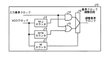
図5は、図1に示した基準クロック調整回路10の構成の一例を示すブロック図である。基準クロック調整回路10は、Mカウンタ11、M−Jカウンタ12、M+Kカウンタ13、アンドゲートであるAND14と、オアゲートであるOR15と、セレクタ16とを備えている。
【0027】
Mカウンタ11は、VCO50で生成した出力クロックであるVCOクロックをM個カウントする。Mカウンタ11は、分周器60と同一の機能であり、フィードバッククロックの代りとなる基準値を生成する。そしてその基準値をセレクタ16に出力する。M−Jカウンタ12は、VCOクロックをM−J(J>0,Jは整数)個カウントする。M+Kカウンタ13は、VCOクロックをM+K(K>0,Kは整数)個カウントする。
【0028】
AND14には、入力基準クロックとM−Jカウンタ12の出力が入力される。AND14は、入力基準クロックの位相が基準値に対して所定の値(この場合VCOクロックJ個分の周期)以上進んでいる場合に入力基準クロックをマスクした調整基準クロックをセレクタ16に出力する。また、入力基準クロックが所定の範囲内である場合に入力基準クロックを出力する。
【0029】
OR15には、入力基準クロックとM+Kカウンタ13の出力が入力される。OR15は、入力基準クロックの位相が基準クロックに対して所定の値(この場合VCOクロックK個分の周期)以上遅れている場合に、その遅れ分を補った値調整基準クロックをセレクタ16に出力する。
【0030】
セレクタ16は、基準値が“L”の場合AND14の出力を選択し、基準値が“H”の場合OR15の出力を選択する。
【0031】
図6および図7のタイムチャートを参照して、基準クロック調整回路10の詳細な動作を説明する。図6は、入力基準クロックの位相が基準値よりも早くなった場合のタイムチャートを示している。図6に示すように、入力基準クロックは基準値よりも早く“H”になっている。しかし、基準値からVCOクロックJ個分以上早いため、M−Jカウンタ12の出力は“L”である。したがって、AND14の出力は“L”のまま変化しない。入力基準クロックが“H”に変化したため、OR15は出力を“H”にする。しかし、基準値は“L”であるのでセレクタ16はAND14の出力を選択し、調整基準クロックは“L”のまま変化しない。
【0032】
M−Jカウンタ12がVCOクロックをM−J個カウントし出力を“H”にする。M−Jカウンタ12の出力が“H”に変化すると、すでに入力基準クロックが“H”であるのでAND14は出力を“H”にする。基準値が“L”であるのでセレクタ16はADN14の出力を選択し、調整基準クロックを“H”にする。これにより、入力基準クロックの位相が基準値よりも早くなった場合でも、所定の範囲内の変動で抑えた調整基準クロックを出力することができる。
【0033】
図7は、入力基準クロックの位相が基準値よりも遅くなった場合のタイムチャートを示している。M−Jカウンタ12がVCOクロックをM−J個カウントして出力を“H”にする。しかし、入力基準クロックが“L”であるのでAND14の出力は“L”のまま変化しない。Mカウンタ11がVCOクロックをM個カウントして出力を“H”にする。Mカウンタ11の出力が“H”に変化するとセレクタ16は、OR15の出力を選択する。しかし、入力基準クロックとM+Kカウンタ13の出力がともに“L”であるので調整基準クロックは“L”のまま変化しない。
【0034】
M+Kカウンタ13がVCOクロックをM+K個カウントし出力を“H”にする。M+Kカウンタ13の出力が“H”に変化するとOR15は出力を“H”にする。すでに基準値が“H”であり、セレクタ16はOR15の出力を選択し、基準調整クロックを“H”にする。これにより、入力基準クロックの位相が基準値よりも遅くなった場合でも、所定の範囲内の変動で抑えた調整基準クロックを出力することができる。
【0035】
このようにこの実施の形態1では、基準クロック調整回路10は、VCO50が生成したクロックを入力基準クロックと同位相になるように1/Mで分周したフィードバッククロックと入力基準クロックとの位相を比較する。そして、比較の結果、入力基準クロックの位相が所定の範囲以上進んだり遅れたりしていた場合には、入力基準クロックを調整した調整基準クロックを位相比較器20に出力する。これにより、入力基準クロックの周波数変動が大きい場合でも、その変動を抑制した調整基準クロックを用いてVCO50が発生するクロック周波数を制御し出力クロックの変動を抑えることができる。
【0036】
なお、位相比較器20は立ち上がりエッジで位相の比較を行うものとしたが、位相の比較は立ち下がりエッジやパルス幅で比較するようにしてもよい。
【0037】
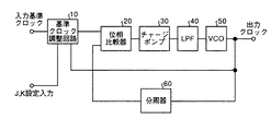
また、図8に示すように、基準クロック調整回路10のカウンタの値を外部から設定できるようにしてもよい。すなわち、図5のM−Jカウンタ12とM+Kカウンタ13のカウント値を外部から設定可能とする。入力基準クロックの周波数変動が、たとえば、周波数が高い方(フィードバッククロックと比較して位相が進む)に変動が大きい場合にはJの値を大きく設定し、Kの値を小さく設定する。周波数が低い方(フィードバッククロックと比較して位相が遅れる)に変動が大きい場合にはJの値を小さく設定し、Kの値を大きく設定する。入力基準クロックの変動が時系列的に変化する場合には、その変動が大きい場合にはJ,Kの値を大きく設定し、変動が小さい場合にはJ,Kの値を小さく設定する。このように、外部からJ,Kの値を設定することにより、より入力基準クロックに近い最適な調整基準クロックを生成することが可能となり、入力基準クロックの変動周期および発生確率に合わせてVCO50を制御して出力クロックの変動を抑えることができる。
【0038】
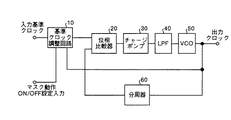
さらに、図9に示すように、基準クロック調整回路10を動作させるか否かを外部から設定できるようにしてもよい。すなわち、位相比較器20がフィードバッククロックと位相比較をするクロックを入力基準クロックを用いるか調整基準クロックを用いるかを外部から設定できるようにする。この設定は、周期的でも任意のタイミングで変更してもよい。たとえば、入力基準クロックの周波数変動が一定周期である場合、周波数変動が小さい期間は基準クロック調整回路10を動作させずに入力基準クロックを用いてVCO50の制御を行い、周波数変動が大きい期間は、基準クロック調整回路10を動作させて変動を抑制した調整基準クロックを用いてVCO50を制御する。これにより、入力基準クロックの変動周期および発生確率に合わせてVCO50を制御して出力クロックの変動を抑えることができる。
【0039】
もちろん、図10に示すようにM−Jカウンタ12とM+Kカウンタ13のカウント値の設定および基準クロック調整回路10を動作させるか否かのON/OFF設定を同時に設定することも可能であり、それらの設定は外部端子によるものではなくJ,Kの値およびON/OFFの信号を生成する設定回路80の信号を用いるようにしてもよい。周期的に入力基準クロックの周波数が変動する場合、設定回路80がその周期毎に設定値を変更するようにする。これにより、入力基準クロックの変動に連動させて基準クロック調整回路10を動作させることができる。
【0040】
実施の形態2.
図11〜図15を用いて本発明の実施の形態2を説明する。実施の形態2では、フィードバッククロックと比較する入力基準クロックを調整することで出力クロックの変動を抑制するようにした。この実施の形態2では、クロックを生成するVCO50を制御する位相誤差信号を調整することで出力クロックの変動を抑制するものである。
【0041】
図11は、この発明の実施の形態2のクロック発生回路の構成を示すブロック図である。図11に示すクロック生成回路は、位相比較器20とチャージポンプ30との間に位相誤差調整回路70(請求の範囲でいうところの調整回路)を備えている。図1と同じ機能を持つ構成部分については同一符号を付し、重複する説明は省略する。
【0042】
位相誤差調整回路70は、位相比較器20が出力した位相誤差信号が所定の値以上VCO50の発振周波数を変化させるような信号である場合、その変化を所定の値内にするように位相誤差信号を調整する。位相誤差信号は、VCO50の発振周波数を上げるためのUP信号とVCO50の発振周波数を下げるためのDOWN信号とがある。位相誤差調整回路70は、UP信号とDOWN信号を調整してVCO50の出力クロックの変動を抑える。
【0043】
VCO50は、UP信号とDOWN信号がともに“H”となると発振周波数を上げるように動作し、UP信号とDOWN信号がともに“L”になると発振周波数を下げるように動作するものとする。
【0044】
図12は、図11に示す位相誤差調整回路70の構成を示すブロック図である。位相誤差調整回路70は、M−Jカウンタ12と、M+Kカウンタ13と、反転回路であるインバータ71,72と、アンドゲートであるAND73,74と、ナンドゲートであるNAND75とを備えている。
【0045】
M−Jカウンタ12は、VCOクロックをM−J(J>1,Jは整数)個カウントする。M+Kカウンタ13は、VCOクロックをM+K(K>1,Kは整数)個カウントする。
【0046】
AND73には、M−Jカウンタ12の出力とM+Kカウンタ13の出力がインバータ72を介したM+Kカウンタ13の出力が入力される。すなわち、このAND73は、周波数変動の所定の範囲内だけMASK信号を“H”にする。
【0047】
AND74には、DOWN信号とAND73の出力MASKが入力されDOWN信号を調整する。NAND75には、インバータ71を介したUP信号とAND73の出力MASKが入力されUP信号を調整する。
【0048】
図13および図14のタイムチャートを参照して、位相誤差調整回路70の詳細な動作を説明する。図13は、入力基準クロックの位相がフィードバッククロックの位相よりも早くなったために、DOWN信号を出力する場合のタイムチャートを示している。図13に示すように、UP信号が“H”から“L”に変化する。これにより、NAND75の一方の入力は“H”となる。しかし、M−Jカウンタ12とM+Kカウンタ13がともに“L”であるため、MASK信号は“L”であり、調整UP信号は“H”のまま変化しない。
【0049】
M−Jカウンタ12がVCOクロックをM−J個カウントし出力を“H”にする。M+Kカウンタ13はVCOクロックをM+K個カウントしていないのでインバータ72を介してAND73には“H”が入力されているため、M−Jカウンタ12の出力が“H”に変化すると、AND73はMASK信号を“H”にする。MASK信号が“H”変化するとインバータ71を介して入力されているUP信号を有効となり、NAND75は調整UP信号を“L”にする。これにより、調整UP信号が“L”、調整DOWN信号が“L”となり、VCO50の周波数を上げるような指定となる。
【0050】
図14は、入力基準クロックの位相がフィードバッククロックの位相よりも遅くなったため、DOWN信号を出力する場合のタイムチャートを示している。M−Jカウンタ12がVCOクロックをM−J個カウントし出力を“H”にする。M+Kカウンタ13はVCOクロックをM+K個カウントしていないので出力は“L”である。したがって、MASK信号は“H”となり、NAND75はUP信号を、AND74はDOWN信号を有効にする。しかし、DOWN信号は“L”であるので調整DOWN信号は“L”のまま変化しない。
【0051】
入力基準クロックの位相がフィードバッククロックの位相よりも遅れているため、VCO50の発振周波数を高くするようにDOWN信号が“H”となると、AND74は、DOWN信号を有効にして調整DOWN信号を“H”にする。
【0052】
M+Kカウンタ13がVCOクロックをM+K個カウントし出力を“H”にする。M+Kカウンタ13の出力が“H”に変化するとAND73はMASK信号を“L”にする。MASK信号が“L”に変化するとAND74は調整DOWN信号を“H”にする。これにより、調整UP信号が“H”、調整DOWN信号が“L”となり、VCO50の発振周波数を下げるような指定が解除される。
【0053】
このようにこの実施の形態2では、位相誤差調整回路70は、位相比較器20から出力されるUP信号とDOWN信号を所定の範囲内だけ有効にするようにしているため、入力基準クロックの周波数変動が大きい場合でも、その変動を抑制した調整UP信号と調整DOWN信号を用いてVCO50が発生するクロック周波数を制御し出力クロックの変動を抑えることができる。
【0054】
なお、図15に示すように、位相誤差調整回路70のカウンタの値を外部から設定できるようにしてもよい。すなわち、図11のM−Jカウンタ12とM+Kカウンタ13のカウント値を外部から設定可能とする。入力基準クロックの周波数変動が、たとえば、周波数が高い方(フィードバッククロックと比較して位相が進む)に変動が大きい場合にはJの値を大きく設定し、Kの値を小さく設定する。周波数が低い方(フィードバッククロックと比較して位相が遅れる)に変動が大きい場合にはJの値を小さく設定し、Kの値を大きく設定する。入力基準クロックの変動が時系列的に変化する場合には、その変動が大きい場合にはJ,Kの値を大きく設定し、変動が小さい場合にはJ,Kの値を小さく設定する。このように、外部からJ,Kの値を設定することにより、入力基準クロックの変動周期および発生確率に合わせてVCO50を制御して出力クロックの変動を抑えることができる。
【0055】
また、位相誤差調整回路70を動作させるか否かを外部から設定できるようにしてもよい。すなわち、位相比較器20が生成したUP信号およびDOWN信号をそのまま用いるか調整を行うかを外部から設定できるようにする。これにより、入力基準クロックの変動周期および発生確率に合わせてVCO50を制御して出力クロックの変動を抑えることができる。
【0056】
さらに、M−Jカウンタ12とM+Kカウンタ13のカウント値の設定および位相誤差調整回路70を動作させるか否かのON/OFF設定を同時に設定することも可能であり、それらの設定は外部端子によるものではなくJ,Kの値およびON/OFFの信号を生成する設定回路から指定するようにしてもよい。周期的に入力基準クロックの周波数が変動する場合、設定回路がその周期毎に設定値を変更するようにする。これにより、入力基準クロックの変動に連動させて基準クロック調整回路10を動作させることができる。
【0057】
【発明の効果】
以上説明したように、この発明にかかるクロック発生回路によれば、調整回路は、電圧制御発振器の出力クロックを所定の値に分周して入力基準クロックと同位相になるように生成したフィードバッククロックを基準として入力基準クロックの位相差が所定の範囲より大きい場合には、その変動を所定の範囲に調整して電圧制御発振器を制御するようにしているため、入力基準クロックの周波数変動が大きい場合でも、電圧制御発振器が生成する出力クロックの変動を抑えることができる。
【図面の簡単な説明】
【図1】この発明にかかるクロック生成回路の実施の形態1の構成の一例を示すブロック図である。
【図2】この発明にかかるクロック生成回路の実施の形態1の動作を説明するためのタイムチャートである。
【図3】この発明にかかるクロック生成回路の実施の形態1の動作を説明するためのタイムチャートである。
【図4】この発明にかかるクロック生成回路の実施の形態1の動作を説明するためのタイムチャートである。
【図5】図1に示した基準クロック調整回路の構成を示すブロック図である。
【図6】基準クロック調整回路の動作を説明するためのタイムチャートである。
【図7】基準クロック調整回路の動作を説明するためのタイムチャートである。
【図8】この発明にかかるクロック生成回路の実施の形態1の構成の一例を示すブロック図である。
【図9】この発明にかかるクロック生成回路の実施の形態1の構成の一例を示すブロック図である。
【図10】この発明にかかるクロック生成回路の実施の形態1の構成の一例を示すブロック図である。
【図11】この発明にかかるクロック生成回路の実施の形態2の構成の一例を示すブロック図である。
【図12】図11に示した位相誤差調整回路の構成を示すブロック図である。
【図13】位相誤差調整回路の動作を説明するためのタイムチャートである。
【図14】位相誤差調整回路の動作を説明するためのタイムチャートである。
【図15】この発明にかかるクロック生成回路の実施の形態2の構成の一例を示すブロック図である。
【符号の説明】
10 基準クロック調整回路、11 Mカウンタ、12 M−Jカウンタ、13 M+Kカウンタ、14,73,74 AND、15 OR、16 セレクタ、20 位相比較器、30 チャージポンプ、40 LPF、50 VCO、60 分周器、70 位相誤差調整回路、71,72 インバータ、75 NAND、80 設定回路。[0001]
TECHNICAL FIELD OF THE INVENTION
The present invention relates to a clock generation circuit configured with a phase locked loop (PLL), and more particularly to a clock generation circuit for suppressing an influence on an output clock when a reference clock has a large frequency fluctuation. It is.
[0002]
[Prior art]
A clock generation circuit using a PLL compares a phase of a feedback clock generated by dividing an output clock of a voltage controlled oscillator (VCO) by a predetermined value with a frequency divider and an input reference clock. The transmission frequency of the VCO is controlled based on the comparison result, and the frequency of the output clock is adjusted. That is, the clock generation circuit using the PLL generates the output clock following the reference clock. Therefore, when the frequency fluctuation of the input reference clock is large, the jitter component included in the output clock becomes large. The removal rate of the frequency fluctuation of the input reference clock to the output clock is determined by the transfer function of the PLL. The transfer function is determined by the conversion gain of the VCO, the conversion gain of the phase comparator, the transfer function of the loop filter for removing the high frequency component of the control signal of the phase comparator, and the division ratio of the frequency divider. A large change in the frequency of the clock, for example, a change longer than the cycle of the output clock cannot be eliminated.
[0003]
In order to solve such a problem, for example, a conventional clock generation circuit counts an edge interval of an input reference clock based on a clock generated by a VCO, and determines whether the count value is within a predetermined range. When it is out of the predetermined range, the operation of the phase comparator is stopped so that the VCO is not controlled, and the fluctuation of the output clock is suppressed. (For example, see Patent Document 1).
[0004]
[Patent Document 1]
JP 2001-53600 A
[0005]
[Problems to be solved by the invention]
However, in the above-described conventional technology, when the frequency fluctuation of the input reference clock is large, the operation of the phase comparator is stopped so that the VCO is not controlled, so that the VCO is controlled over a plurality of cycles of the input reference clock. Therefore, the output clock is generated without causing a problem that the jitter component of the output clock increases. Further, the edge of the input reference clock is counted based on the output clock with the increased jitter component, and there is a problem that the accuracy of the determination in the predetermined range is deteriorated.
[0006]
The present invention has been made in view of the above, and an object of the present invention is to provide a clock generation circuit that suppresses fluctuation of a generated clock by controlling the oscillation frequency of a VCO within a predetermined range when the frequency fluctuation of an input reference clock is large. The purpose is.
[0007]
[Means for Solving the Problems]
In order to achieve the above object, a feedback clock obtained by dividing an output clock of a voltage controlled oscillator to a predetermined value is generated by a frequency divider, and a phase comparator detects a phase difference between the feedback clock and an input reference clock. In a clock generation circuit using a phase-locked loop that generates a phase error signal for eliminating a leverage phase difference and controls an output clock of the voltage controlled oscillator, when a frequency fluctuation of the input reference clock is larger than a predetermined range. And an adjusting circuit for adjusting the frequency variation within a predetermined range.
[0008]
According to the present invention, the adjustment circuit divides the output clock of the voltage controlled oscillator to a predetermined value and sets the phase difference of the input reference clock to a predetermined value based on the feedback clock generated so as to have the same phase as the input reference clock. Is larger than the range, the fluctuation is adjusted to a predetermined range to control the voltage-controlled oscillator.
[0009]
BEST MODE FOR CARRYING OUT THE INVENTION
Hereinafter, preferred embodiments of a clock generation circuit according to the present invention will be described in detail with reference to the accompanying drawings.
[0010]
Embodiment 1 FIG.
Embodiment 1 of the present invention will be described with reference to FIGS. FIG. 1 is a block diagram showing a configuration of the clock generation circuit according to the first embodiment of the present invention. The clock generation circuit according to the first embodiment includes a reference clock adjustment circuit 10 (an adjustment circuit referred to in the claims), a
[0011]
The reference
[0012]
The
[0013]
The
[0014]
The
[0015]
The VCO 50 performs transmission control based on the phase error signal whose high-frequency component has been cut off by the
[0016]
The
[0017]
An outline of the operation of the clock generation circuit according to the first embodiment will be described with reference to time charts of FIGS. FIG. 2 is a time chart when the frequency fluctuation of the input reference clock is within one cycle of the output clock with respect to the feedback clock. In FIG. 2, the input reference clock lags behind the feedback clock by the difference a. Since the difference a is within one cycle of the output clock, the reference
[0018]
FIG. 3A is a time chart when the frequency fluctuation of the input reference clock is delayed by one or more output clock cycles with respect to the feedback clock. In FIG. 3A, the input reference clock lags behind the feedback clock by a difference a. Since the difference a is equal to or more than one cycle of the output clock, the reference
[0019]
FIG. 4A is a time chart in the case where the frequency fluctuation of the input reference clock leads the output clock by one or more cycles of the output clock. In FIG. 4A, the input reference clock leads the difference a with respect to the feedback clock. Since the difference a is equal to or more than one cycle of the output clock, the reference
[0020]
As described above, when the frequency fluctuation of the input reference clock is large, the reference
[0021]
The
[0022]
The
[0023]
The
[0024]
The
[0025]
The
[0026]
FIG. 5 is a block diagram showing an example of the configuration of the reference
[0027]
The M counter 11 counts M VCO clocks, which are output clocks generated by the
[0028]
The input reference clock and the output of the
[0029]
The input reference clock and the output of the M + K counter 13 are input to the
[0030]
The
[0031]
The detailed operation of the reference
[0032]
The MJ counter 12 counts MJ VCO clocks and sets the output to “H”. When the output of the MJ counter 12 changes to "H", the AND 14 changes the output to "H" because the input reference clock is already "H". Since the reference value is "L", the
[0033]
FIG. 7 shows a time chart when the phase of the input reference clock is later than the reference value. The MJ counter 12 counts MJ VCO clocks and sets the output to “H”. However, since the input reference clock is "L", the output of the AND 14 remains "L". The M counter 11 counts M VCO clocks and changes the output to “H”. When the output of the M counter 11 changes to “H”, the
[0034]
The M + K counter 13 counts M + K VCO clocks and sets the output to “H”. When the output of the M + K counter 13 changes to "H", the
[0035]
As described above, in the first embodiment, the reference
[0036]
Although the
[0037]
Further, as shown in FIG. 8, the value of the counter of the reference
[0038]
Further, as shown in FIG. 9, whether or not to operate the reference
[0039]
Of course, as shown in FIG. 10, the setting of the count values of the
[0040]
[0041]
FIG. 11 is a block diagram showing a configuration of the clock generation circuit according to the second embodiment of the present invention. The clock generation circuit shown in FIG. 11 includes a phase error adjustment circuit 70 (an adjustment circuit in claims) between the
[0042]
When the phase error signal output from the
[0043]
The
[0044]
FIG. 12 is a block diagram showing a configuration of the phase
[0045]
The MJ counter 12 counts MJ (J> 1, J is an integer) VCO clocks. The M + K counter 13 counts M + K (K> 1, K is an integer) VCO clocks.
[0046]
The output of the
[0047]
The AND 74 receives the DOWN signal and the output MASK of the AND 73 and adjusts the DOWN signal. The
[0048]
The detailed operation of the phase
[0049]
The MJ counter 12 counts MJ VCO clocks and sets the output to “H”. Since the M +
[0050]
FIG. 14 shows a time chart when the DOWN signal is output because the phase of the input reference clock is later than the phase of the feedback clock. The MJ counter 12 counts MJ VCO clocks and sets the output to “H”. Since the M +
[0051]
Since the phase of the input reference clock is behind the phase of the feedback clock, when the DOWN signal becomes “H” so as to increase the oscillation frequency of the
[0052]
The M + K counter 13 counts M + K VCO clocks and sets the output to “H”. When the output of the M + K counter 13 changes to "H", the AND 73 changes the MASK signal to "L". When the MASK signal changes to “L”, the AND 74 sets the adjustment DOWN signal to “H”. As a result, the adjustment UP signal becomes “H” and the adjustment DOWN signal becomes “L”, and the designation of lowering the oscillation frequency of the
[0053]
As described above, in the second embodiment, the phase
[0054]
As shown in FIG. 15, the counter value of the phase
[0055]
Further, whether or not to operate the phase
[0056]
Further, the setting of the count values of the
[0057]
【The invention's effect】
As described above, according to the clock generation circuit of the present invention, the adjustment circuit divides the output clock of the voltage controlled oscillator to a predetermined value and generates the feedback clock generated so as to have the same phase as the input reference clock. When the phase difference of the input reference clock is larger than a predetermined range with respect to the reference, the fluctuation is adjusted to the predetermined range to control the voltage-controlled oscillator. However, fluctuations in the output clock generated by the voltage controlled oscillator can be suppressed.
[Brief description of the drawings]
FIG. 1 is a block diagram illustrating an example of a configuration of a clock generating circuit according to a first embodiment of the present invention;
FIG. 2 is a time chart for explaining an operation of the clock generating circuit according to the first embodiment of the present invention;
FIG. 3 is a time chart for explaining the operation of the clock generating circuit according to the first embodiment of the present invention;
FIG. 4 is a time chart for explaining the operation of the clock generating circuit according to the first embodiment of the present invention;
FIG. 5 is a block diagram illustrating a configuration of a reference clock adjustment circuit illustrated in FIG. 1;
FIG. 6 is a time chart for explaining the operation of the reference clock adjustment circuit.
FIG. 7 is a time chart for explaining the operation of the reference clock adjustment circuit.
FIG. 8 is a block diagram illustrating an example of a configuration of a clock generation circuit according to a first embodiment of the present invention;
FIG. 9 is a block diagram illustrating an example of a configuration of a clock generation circuit according to the first embodiment of the present invention;
FIG. 10 is a block diagram illustrating an example of a configuration of a clock generation circuit according to a first embodiment of the present invention;
FIG. 11 is a block diagram illustrating an example of a configuration of a clock generation circuit according to a second embodiment of the present invention;
FIG. 12 is a block diagram showing a configuration of a phase error adjustment circuit shown in FIG.
FIG. 13 is a time chart for explaining the operation of the phase error adjustment circuit.
FIG. 14 is a time chart for explaining the operation of the phase error adjustment circuit.
FIG. 15 is a block diagram illustrating an example of a configuration of a clock generation circuit according to a second embodiment of the present invention;
[Explanation of symbols]
10 Reference clock adjustment circuit, 11 M counter, 12 M-J counter, 13 M + K counter, 14, 73, 74 AND, 15 OR, 16 selector, 20 phase comparator, 30 charge pump, 40 LPF, 50 VCO, 60 minutes Frequency divider, 70 phase error adjustment circuit, 71, 72 inverter, 75 NAND, 80 setting circuit.
Claims (8)
前記入力基準クロックの周波数変動が所定の範囲より大きい場合、該周波数変動を所定の範囲内に調整する調整回路、
を備えることを特徴とするクロック発生回路。A frequency divider generates a feedback clock obtained by dividing the output clock of the voltage controlled oscillator to a predetermined value. In a clock generation circuit using a phase locked loop that generates a phase error signal and controls an output clock of the voltage controlled oscillator,
An adjusting circuit that adjusts the frequency fluctuation within a predetermined range when the frequency fluctuation of the input reference clock is larger than a predetermined range;
A clock generation circuit comprising:
前記入力基準クロックと前記フィードバッククロックの位相差が所定の範囲内の場合には前記位相比較器に前記入力基準クロックを出力し、前記入力基準クロックと前記フィードバッククロックの位相差が所定の範囲外の場合には位相比較器に前記入力基準クロックの位相が所定の範囲内になるように調整した調整基準クロックを出力することを特徴とする請求項1に記載のクロック発生回路。The adjustment circuit includes:
When the phase difference between the input reference clock and the feedback clock is within a predetermined range, the input reference clock is output to the phase comparator, and the phase difference between the input reference clock and the feedback clock is out of a predetermined range. 2. The clock generation circuit according to claim 1, wherein in such a case, an adjusted reference clock adjusted so that the phase of the input reference clock falls within a predetermined range is output to a phase comparator.
前記位相誤差信号のアサート状態が所定の範囲内の場合には電圧制御発振器に該位相誤差信号を出力し、所定の範囲外に前記位相誤差信号がアサート状態になった場合にはそのアサート状態をネゲート状態に変えて電圧制御発振器に出力することを特徴とする請求項1に記載のクロック発生回路。The adjustment circuit includes:
When the asserted state of the phase error signal is within a predetermined range, the phase error signal is output to the voltage-controlled oscillator. 2. The clock generating circuit according to claim 1, wherein the clock generating circuit outputs the signal to a voltage-controlled oscillator after changing to a negated state.
を備えたことを特徴とする請求項4または7に記載のクロック発生回路。A setting circuit that periodically changes the setting of the number of clock cycles of the voltage-controlled oscillator that specifies the predetermined range and / or the setting of whether to operate the adjustment circuit;
The clock generation circuit according to claim 4, further comprising:
Priority Applications (1)
| Application Number | Priority Date | Filing Date | Title |
|---|---|---|---|
| JP2002313314A JP2004153332A (en) | 2002-10-28 | 2002-10-28 | Clock generating circuit |
Applications Claiming Priority (1)
| Application Number | Priority Date | Filing Date | Title |
|---|---|---|---|
| JP2002313314A JP2004153332A (en) | 2002-10-28 | 2002-10-28 | Clock generating circuit |
Publications (1)
| Publication Number | Publication Date |
|---|---|
| JP2004153332A true JP2004153332A (en) | 2004-05-27 |
Family
ID=32457960
Family Applications (1)
| Application Number | Title | Priority Date | Filing Date |
|---|---|---|---|
| JP2002313314A Pending JP2004153332A (en) | 2002-10-28 | 2002-10-28 | Clock generating circuit |
Country Status (1)
| Country | Link |
|---|---|
| JP (1) | JP2004153332A (en) |
Cited By (5)
| Publication number | Priority date | Publication date | Assignee | Title |
|---|---|---|---|---|
| JP2009065631A (en) * | 2007-08-10 | 2009-03-26 | Hitachi Kokusai Electric Inc | Signal reproduction device |
| JP2012154841A (en) * | 2011-01-27 | 2012-08-16 | Mitsubishi Electric Corp | Gps jitter reduction device |
| US9252749B2 (en) | 2013-10-31 | 2016-02-02 | Seiko Epson Corporation | Clock generation device, electronic apparatus, moving object, and clock generation method |
| US9389636B2 (en) | 2013-10-31 | 2016-07-12 | Seiko Epson Corporation | Clock generating device, electronic apparatus, moving object, clock generating method |
| WO2020012550A1 (en) * | 2018-07-10 | 2020-01-16 | 株式会社ソシオネクスト | Phase synchronization circuit, transmission and reception circuit, and integrated circuit |
-
2002
- 2002-10-28 JP JP2002313314A patent/JP2004153332A/en active Pending
Cited By (8)
| Publication number | Priority date | Publication date | Assignee | Title |
|---|---|---|---|---|
| JP2009065631A (en) * | 2007-08-10 | 2009-03-26 | Hitachi Kokusai Electric Inc | Signal reproduction device |
| JP2012154841A (en) * | 2011-01-27 | 2012-08-16 | Mitsubishi Electric Corp | Gps jitter reduction device |
| US9252749B2 (en) | 2013-10-31 | 2016-02-02 | Seiko Epson Corporation | Clock generation device, electronic apparatus, moving object, and clock generation method |
| US9389636B2 (en) | 2013-10-31 | 2016-07-12 | Seiko Epson Corporation | Clock generating device, electronic apparatus, moving object, clock generating method |
| WO2020012550A1 (en) * | 2018-07-10 | 2020-01-16 | 株式会社ソシオネクスト | Phase synchronization circuit, transmission and reception circuit, and integrated circuit |
| JPWO2020012550A1 (en) * | 2018-07-10 | 2021-08-02 | 株式会社ソシオネクスト | Phase-locked loop, transceiver circuit and integrated circuit |
| JP7174271B2 (en) | 2018-07-10 | 2022-11-17 | 株式会社ソシオネクスト | Phase locked loop, transmitter/receiver circuit and integrated circuit |
| US11777701B2 (en) | 2018-07-10 | 2023-10-03 | Socionext Inc. | Phase synchronization circuit, transmission and reception circuit, and integrated circuit |
Similar Documents
| Publication | Publication Date | Title |
|---|---|---|
| US8085101B2 (en) | Spread spectrum clock generation device | |
| JP2795323B2 (en) | Phase difference detection circuit | |
| US7881419B2 (en) | Semiconductor device, spread spectrum clock generator and method thereof | |
| CN100566173C (en) | A clock generation circuit using a spectrum diffusion method capable of high-precision frequency modulation | |
| US7177611B2 (en) | Hybrid control of phase locked loops | |
| US8988121B2 (en) | Method and apparatus for generating a reference signal for a fractional-N frequency synthesizer | |
| US7558311B2 (en) | Spread spectrum clock generator and method for generating a spread spectrum clock signal | |
| US6642800B2 (en) | Spurious-free fractional-N frequency synthesizer with multi-phase network circuit | |
| JP4390353B2 (en) | Clock generation method and clock generation circuit | |
| US8786329B1 (en) | Method for doubling the frequency of a reference clock | |
| US20200220550A1 (en) | PLL with Wide Frequency Coverage | |
| US20080136532A1 (en) | Phase locked loop with adaptive phase error compensation | |
| JPH11316616A (en) | Clock signal supply method and device | |
| US7276944B2 (en) | Clock generation circuit and clock generation method | |
| JP2006024110A (en) | Spread spectrum clock generator and its modulation method | |
| WO2003065586A3 (en) | Phase-locked-loop with reduced clock jitter | |
| US6967536B2 (en) | Phase-locked loop circuit reducing steady state phase error | |
| US6842056B1 (en) | Cascaded phase-locked loops | |
| JP2004153332A (en) | Clock generating circuit | |
| JP2017169109A (en) | Clock generation circuit and clock generation method | |
| CN1866746B (en) | System and method for optimizing damping coefficient of phase-locked loop | |
| US8502574B2 (en) | Device and method for generating a signal of parametrizable frequency | |
| JP2001230667A (en) | Phase control circuit | |
| JPH07154246A (en) | Phase-locked loop and operation method | |
| JP3161137B2 (en) | PLL circuit |