JP2004144826A - Liquid crystal display device and method for manufacturing the same - Google Patents
Liquid crystal display device and method for manufacturing the same Download PDFInfo
- Publication number
- JP2004144826A JP2004144826A JP2002306991A JP2002306991A JP2004144826A JP 2004144826 A JP2004144826 A JP 2004144826A JP 2002306991 A JP2002306991 A JP 2002306991A JP 2002306991 A JP2002306991 A JP 2002306991A JP 2004144826 A JP2004144826 A JP 2004144826A
- Authority
- JP
- Japan
- Prior art keywords
- film
- electrode
- liquid crystal
- crystal display
- display device
- Prior art date
- Legal status (The legal status is an assumption and is not a legal conclusion. Google has not performed a legal analysis and makes no representation as to the accuracy of the status listed.)
- Pending
Links
- 239000004973 liquid crystal related substance Substances 0.000 title claims abstract description 67
- 238000000034 method Methods 0.000 title claims abstract description 50
- 238000004519 manufacturing process Methods 0.000 title claims description 53
- 229920002120 photoresistant polymer Polymers 0.000 claims abstract description 77
- 238000000059 patterning Methods 0.000 claims abstract description 22
- 239000010408 film Substances 0.000 claims description 310
- 239000000758 substrate Substances 0.000 claims description 27
- 239000010409 thin film Substances 0.000 claims description 24
- 238000000151 deposition Methods 0.000 claims description 21
- 239000011229 interlayer Substances 0.000 claims description 20
- 239000010410 layer Substances 0.000 claims description 13
- 229910052804 chromium Inorganic materials 0.000 claims description 11
- 238000005530 etching Methods 0.000 claims description 11
- 229910052735 hafnium Inorganic materials 0.000 claims description 8
- 229910052715 tantalum Inorganic materials 0.000 claims description 8
- 229910052719 titanium Inorganic materials 0.000 claims description 8
- 229910052726 zirconium Inorganic materials 0.000 claims description 8
- 229910052750 molybdenum Inorganic materials 0.000 claims description 7
- 229910000838 Al alloy Inorganic materials 0.000 claims description 6
- 230000005540 biological transmission Effects 0.000 claims description 6
- 229910052710 silicon Inorganic materials 0.000 claims description 6
- 229910052721 tungsten Inorganic materials 0.000 claims description 6
- 229910052779 Neodymium Inorganic materials 0.000 claims description 5
- 229910052706 scandium Inorganic materials 0.000 claims description 5
- 229910052727 yttrium Inorganic materials 0.000 claims description 5
- 229910052738 indium Inorganic materials 0.000 claims description 4
- 229910045601 alloy Inorganic materials 0.000 claims description 3
- 239000000956 alloy Substances 0.000 claims description 3
- 229910052802 copper Inorganic materials 0.000 claims description 3
- 229910052759 nickel Inorganic materials 0.000 claims description 3
- 229910052763 palladium Inorganic materials 0.000 claims description 3
- 239000002356 single layer Substances 0.000 claims description 3
- 229910001316 Ag alloy Inorganic materials 0.000 claims description 2
- 229910052725 zinc Inorganic materials 0.000 claims description 2
- 230000007797 corrosion Effects 0.000 abstract description 36
- 238000005260 corrosion Methods 0.000 abstract description 36
- 238000006243 chemical reaction Methods 0.000 abstract description 24
- VYPSYNLAJGMNEJ-UHFFFAOYSA-N Silicium dioxide Chemical compound O=[Si]=O VYPSYNLAJGMNEJ-UHFFFAOYSA-N 0.000 description 29
- 150000002500 ions Chemical class 0.000 description 21
- 238000010586 diagram Methods 0.000 description 18
- 229910021420 polycrystalline silicon Inorganic materials 0.000 description 18
- 229910052681 coesite Inorganic materials 0.000 description 14
- 229910052906 cristobalite Inorganic materials 0.000 description 14
- 239000000377 silicon dioxide Substances 0.000 description 14
- 235000012239 silicon dioxide Nutrition 0.000 description 14
- 229910052682 stishovite Inorganic materials 0.000 description 14
- 229910052905 tridymite Inorganic materials 0.000 description 14
- 239000011651 chromium Substances 0.000 description 13
- 238000001312 dry etching Methods 0.000 description 13
- 229910021417 amorphous silicon Inorganic materials 0.000 description 11
- 239000000463 material Substances 0.000 description 11
- 230000000694 effects Effects 0.000 description 9
- 239000011521 glass Substances 0.000 description 9
- 238000000206 photolithography Methods 0.000 description 9
- 238000004544 sputter deposition Methods 0.000 description 9
- 229910052581 Si3N4 Inorganic materials 0.000 description 7
- 229910004298 SiO 2 Inorganic materials 0.000 description 7
- 238000004380 ashing Methods 0.000 description 5
- 239000002585 base Substances 0.000 description 5
- 238000005229 chemical vapour deposition Methods 0.000 description 5
- 230000007547 defect Effects 0.000 description 5
- 238000004090 dissolution Methods 0.000 description 5
- 229910021424 microcrystalline silicon Inorganic materials 0.000 description 5
- 230000002093 peripheral effect Effects 0.000 description 5
- 238000001039 wet etching Methods 0.000 description 5
- 229910000789 Aluminium-silicon alloy Inorganic materials 0.000 description 4
- 239000003513 alkali Substances 0.000 description 4
- 229910052782 aluminium Inorganic materials 0.000 description 4
- QVGXLLKOCUKJST-UHFFFAOYSA-N atomic oxygen Chemical compound [O] QVGXLLKOCUKJST-UHFFFAOYSA-N 0.000 description 4
- 238000009792 diffusion process Methods 0.000 description 4
- 238000002513 implantation Methods 0.000 description 4
- 230000033116 oxidation-reduction process Effects 0.000 description 4
- 239000001301 oxygen Substances 0.000 description 4
- 229910052760 oxygen Inorganic materials 0.000 description 4
- XLYOFNOQVPJJNP-UHFFFAOYSA-N water Substances O XLYOFNOQVPJJNP-UHFFFAOYSA-N 0.000 description 4
- VYZAMTAEIAYCRO-UHFFFAOYSA-N Chromium Chemical compound [Cr] VYZAMTAEIAYCRO-UHFFFAOYSA-N 0.000 description 3
- VEXZGXHMUGYJMC-UHFFFAOYSA-N Hydrochloric acid Chemical compound Cl VEXZGXHMUGYJMC-UHFFFAOYSA-N 0.000 description 3
- 230000001133 acceleration Effects 0.000 description 3
- XAGFODPZIPBFFR-UHFFFAOYSA-N aluminium Chemical compound [Al] XAGFODPZIPBFFR-UHFFFAOYSA-N 0.000 description 3
- 239000004020 conductor Substances 0.000 description 3
- 238000011109 contamination Methods 0.000 description 3
- 238000007796 conventional method Methods 0.000 description 3
- 239000002019 doping agent Substances 0.000 description 3
- 238000010438 heat treatment Methods 0.000 description 3
- 239000011159 matrix material Substances 0.000 description 3
- 238000006722 reduction reaction Methods 0.000 description 3
- 239000004065 semiconductor Substances 0.000 description 3
- 239000010703 silicon Substances 0.000 description 3
- 239000000126 substance Substances 0.000 description 3
- NBIIXXVUZAFLBC-UHFFFAOYSA-N Phosphoric acid Chemical compound OP(O)(O)=O NBIIXXVUZAFLBC-UHFFFAOYSA-N 0.000 description 2
- XUIMIQQOPSSXEZ-UHFFFAOYSA-N Silicon Chemical compound [Si] XUIMIQQOPSSXEZ-UHFFFAOYSA-N 0.000 description 2
- 239000002253 acid Substances 0.000 description 2
- 230000004913 activation Effects 0.000 description 2
- 229910052796 boron Inorganic materials 0.000 description 2
- 239000013078 crystal Substances 0.000 description 2
- 230000008034 disappearance Effects 0.000 description 2
- 238000002845 discoloration Methods 0.000 description 2
- 238000010292 electrical insulation Methods 0.000 description 2
- 230000005611 electricity Effects 0.000 description 2
- 239000001257 hydrogen Substances 0.000 description 2
- 229910052739 hydrogen Inorganic materials 0.000 description 2
- 238000005984 hydrogenation reaction Methods 0.000 description 2
- 239000012535 impurity Substances 0.000 description 2
- 239000007791 liquid phase Substances 0.000 description 2
- 239000002245 particle Substances 0.000 description 2
- 229910052698 phosphorus Inorganic materials 0.000 description 2
- 238000002834 transmittance Methods 0.000 description 2
- ZOXJGFHDIHLPTG-UHFFFAOYSA-N Boron Chemical compound [B] ZOXJGFHDIHLPTG-UHFFFAOYSA-N 0.000 description 1
- KZBUYRJDOAKODT-UHFFFAOYSA-N Chlorine Chemical compound ClCl KZBUYRJDOAKODT-UHFFFAOYSA-N 0.000 description 1
- ZAMOUSCENKQFHK-UHFFFAOYSA-N Chlorine atom Chemical compound [Cl] ZAMOUSCENKQFHK-UHFFFAOYSA-N 0.000 description 1
- UFHFLCQGNIYNRP-UHFFFAOYSA-N Hydrogen Chemical compound [H][H] UFHFLCQGNIYNRP-UHFFFAOYSA-N 0.000 description 1
- ZOKXTWBITQBERF-UHFFFAOYSA-N Molybdenum Chemical compound [Mo] ZOKXTWBITQBERF-UHFFFAOYSA-N 0.000 description 1
- OAICVXFJPJFONN-UHFFFAOYSA-N Phosphorus Chemical compound [P] OAICVXFJPJFONN-UHFFFAOYSA-N 0.000 description 1
- 238000010521 absorption reaction Methods 0.000 description 1
- PNEYBMLMFCGWSK-UHFFFAOYSA-N aluminium oxide Inorganic materials [O-2].[O-2].[O-2].[Al+3].[Al+3] PNEYBMLMFCGWSK-UHFFFAOYSA-N 0.000 description 1
- 229910000147 aluminium phosphate Inorganic materials 0.000 description 1
- 230000000903 blocking effect Effects 0.000 description 1
- 239000002800 charge carrier Substances 0.000 description 1
- 239000000460 chlorine Substances 0.000 description 1
- 229910052801 chlorine Inorganic materials 0.000 description 1
- 238000004140 cleaning Methods 0.000 description 1
- 229910052593 corundum Inorganic materials 0.000 description 1
- 229910021419 crystalline silicon Inorganic materials 0.000 description 1
- 238000006356 dehydrogenation reaction Methods 0.000 description 1
- 239000000539 dimer Substances 0.000 description 1
- 238000009826 distribution Methods 0.000 description 1
- 230000005684 electric field Effects 0.000 description 1
- 238000003487 electrochemical reaction Methods 0.000 description 1
- 239000003792 electrolyte Substances 0.000 description 1
- 238000005516 engineering process Methods 0.000 description 1
- 230000002349 favourable effect Effects 0.000 description 1
- 239000007789 gas Substances 0.000 description 1
- 150000002431 hydrogen Chemical class 0.000 description 1
- 125000004435 hydrogen atom Chemical group [H]* 0.000 description 1
- APFVFJFRJDLVQX-UHFFFAOYSA-N indium atom Chemical compound [In] APFVFJFRJDLVQX-UHFFFAOYSA-N 0.000 description 1
- AMGQUBHHOARCQH-UHFFFAOYSA-N indium;oxotin Chemical compound [In].[Sn]=O AMGQUBHHOARCQH-UHFFFAOYSA-N 0.000 description 1
- 239000012212 insulator Substances 0.000 description 1
- 238000005468 ion implantation Methods 0.000 description 1
- 238000005224 laser annealing Methods 0.000 description 1
- 230000000873 masking effect Effects 0.000 description 1
- 229910021645 metal ion Inorganic materials 0.000 description 1
- 239000000203 mixture Substances 0.000 description 1
- 239000011733 molybdenum Substances 0.000 description 1
- 239000000178 monomer Substances 0.000 description 1
- 230000003287 optical effect Effects 0.000 description 1
- TWNQGVIAIRXVLR-UHFFFAOYSA-N oxo(oxoalumanyloxy)alumane Chemical compound O=[Al]O[Al]=O TWNQGVIAIRXVLR-UHFFFAOYSA-N 0.000 description 1
- 230000035699 permeability Effects 0.000 description 1
- 239000011574 phosphorus Substances 0.000 description 1
- 238000006479 redox reaction Methods 0.000 description 1
- HQVNEWCFYHHQES-UHFFFAOYSA-N silicon nitride Chemical compound N12[Si]34N5[Si]62N3[Si]51N64 HQVNEWCFYHHQES-UHFFFAOYSA-N 0.000 description 1
- 229910052814 silicon oxide Inorganic materials 0.000 description 1
- 229910001845 yogo sapphire Inorganic materials 0.000 description 1
Images


Landscapes
- Liquid Crystal (AREA)
Abstract
Description
【0001】
【発明の属する技術分野】
本発明は、液晶表示装置に関し、特に半透過型液晶表示装置の画素電極構造とその製造方法に関する。
【0002】
【従来の技術】
近年、半導体層にp−Si(poly−Silicon:多結晶シリコン)膜を使用したTFT(Thin Film Transistor:薄膜トランジスタ)、すなわちp−Si TFTを画素スイッチング素子に使用したAMLCD(Active Matrix Liquid Crystal Display:アクティブマトリクス方式液晶表示装置)の開発が盛んに行われている。
【0003】
特にp−Si TFTは、半導体層にa−Si(amorphous−Silicon:非晶質シリコン)膜を使用したTFT、すなわちa−Si TFTよりもキャリア移動度が数桁高いため、AMLCDの画素スイッチング素子としてだけでなく、周辺駆動回路素子としても使用でき、且つガラス基板上に形成できることから、いわゆるSOI(Silicon On Insulator)技術としても活発に研究が進められている。
【0004】
一般に透過型および半透過型の液晶表示装置の透明画素電極には、可視光透過率の高いITO(Indium Tin Oxide)膜が用いられている。また半透過型および反射型の液晶表示装置の反射画素電極には、可視光反射率の高いAl(アルミ)膜が用いられている。特にAl膜は、電気抵抗率が3μΩ・cm前後と低いため、配線材料としても使用されている。
【0005】
以降、図を用いて、特に半透過型AMLCDの画素部に関する従来構造とその製造方法を説明する。まず図19示すように、ガラス基板上1に下地SiO2(酸化シリコン)膜2、a−Si膜、表面SiO2膜を順次堆積した後、ガラス基1板全面にn型TFTの閾値電圧調整用のB(ボロン)関連イオンを注入し、次いでp型TFT部(図示せず)のみにp型TFT(図示せず)の閾値電圧調整用のP(リン)関連イオンを注入する。その後、表面SiO2膜を除去し、次いでa−Si膜を溶融状態から液相結晶成長させてp−Si膜3化すると同時に注入元素の拡散と活性化を行う。
【0006】
次に図20に示すように、p−Si膜3上に界面SiO2膜4を堆積した後、n型TFT部およびp型TFT部(図示せず)の界面SiO2膜4とp−Si膜3を同時にアイランド化する。
【0007】
次に図21に示すように、アイランド部を含むガラス基1板上にゲートSiO2膜5、μc−Si(μ crystal−Silicon:微結晶シリコン)膜6、Cr(クロム)膜7を順次堆積した後、Cr膜7とμc−Si膜6を同時にパターニングしてゲート電極7を形成する。
【0008】
次に図22に示すように、n型TFT部のアイランド部、つまりp−Si膜3部のゲート電極7よりもやや広い領域にP関連イオンを注入してSD(Source Drain)領域8を形成した後、同じn型TFT部のアイランド部、つまりp−Si膜3部にSD領域8よりも少ない濃度でP関連イオンをゲート電極7に対して自己整合的に注入してLDD(Lightly Doped Drain)領域9を形成し、次いでp型TFT部(図示せず)のアイランド部、つまりp−Si膜3部にB関連イオンをゲート電極7に対して自己整合的に注入してSD領域8を形成する。
【0009】
次に図23に示すように、ガラス基板1上に層間SiO2膜10を堆積した後、熱処理によるn型TFT部とp型TFT部(図示せず)のSD領域8の低抵抗化を行い、次いで水素拡散処理による各膜中および各膜界面の低欠陥密度化を行う。そして、n型TFT部とp型TFT部(図示せず)のSD領域8部とゲート電極端子部(図示せず)にコンタクトホールを形成した後、層間SiO2膜10上にAlSi(シリコン含有アルミ)膜17、Mo(モリブデン)膜18を順次堆積し、次いでMo膜18とAlSi膜17を同時にパターニングしてソース・ドレイン電極17,18を形成する。
【0010】
次に図24に示すように、ガラス基板1上に層間Si3N4(窒化シリコン)膜12を堆積した後、画素スイッチング素子用のn型TFT部のドレイン電極部(画素電極接続部)とゲート電極端子接続部(図示せず)およびソース・ドレイン電極端子接続部(図示せず)にコンタクトホールを形成する。
【0011】
その後、図25に示すように全面にITO膜16を堆積した後、ITO膜16をパターニングして透明画素電極16を形成する。
【0012】
次に図26に示すように、全面にMo膜13とAl膜14を順次堆積した後、フォトレジストパターン15を形成して、Al膜14とMo膜13を同時にパターニングする。
【0013】
その後、図27に示すように、フォトレジストパターン15を除去すると、従来技術の半透過型画素電極の構成が得られる。
【0014】
上述のようなTFT基板と対向基板とが対面して張り合わされ、その基板間に電気的および光学的異方性を有する液晶が封止されて半透過型液晶表示装置ができあがる。このような半透過型液晶表示装置は、暗所環境では、主にバックライトからの透過光を利用して、明所環境では、主に外周光からの反射光を利用して画像表示を行うことができる。このため、このような半透過型AMLCDは、屋外、屋内を問わず頻用される携帯電話や携帯情報端末、さらにはノート型PC(パーソナルコンピュータ)等の画像表示装置として使用される場合が多い。
【0015】
上述において、TFTの製造工程には、高解像度が得られると言う理由から、通常ポジ型のフォトレジストが使用される。そして、その現像液には、有機アルカリ溶液が用いられる。この現像液は、一般にph(ペーハー)12〜14の強アルカリ性であるため、酸・アルカリに可溶であるAl膜は、フォトレジスト膜の現像中に3価の金属イオンとなって溶解してしまう。
【0016】
一方、ITO膜は、現像液には不溶であるが、ITO膜の酸化還元電位がAl膜のそれよりも貴側(正側)、言い換えればAl膜の酸化還元電位がITO膜のそれよりも卑側(負側)で、且つ両者の酸化還元電位差が大きいため、電解質(イオンが電荷担体となって電気を通じる媒質)である現像液中でAl膜とITO膜が電気的に接続していると、両者の間で現像液を介した電流回路が形成されてしまい、Al膜の溶解に伴って放出された電子がITO膜に流れ込んでITO膜を還元してしまう。
【0017】
より詳しくは、フォトレジスト膜の現像時にAl膜が溶解して局所的に生じたピンホール等を通じて現像液がITO膜にまで到達し、現像液を介してAl膜を局部アノード、ITO膜を局部カソードとした電流回路が形成され、Al膜とITO膜の酸化還元電位差を反応の駆動力としたAl膜の溶解反応とITO膜の還元反応が進行してしまう。この反応は電池腐食反応と呼ばれ、この問題を解決する技術が、例えば実用新案登録第2539324号公報に記載されている。すなわち、AL膜とITO膜との間にクロム膜を挿入して、上述の問題を解決しようとしたものである。上述では、クロムの代わりにMoを使用した従来技術を紹介した。
【0018】
【特許文献1】
実用新案登録第2539324号公報(第1−2図)
【0019】
また、電池腐食反応の問題が仮に無くても、一般にAl膜とITO膜との間で安定した電気接触を直接とることは難しい。それは、AlとIn(インジウム)の酸化物生成エネルギーの関係がAl>Inであるためで、ITO膜上にAl膜を、あるいは表面酸化膜を除去したAl膜上にITO膜を堆積した後に150℃以上の熱履歴を経験してしまうと、両者の接触界面で電気抵抗率の小さいIn酸化物よりも電気抵抗率の大きいAl酸化物の方が優先的に形成されてしまい、両者が電気絶縁状態になってしまうからである。
【0020】
上述の観点から、光反射電極にアルミを用い、光透過電極にITOを用いた範透過型液晶表示装置の画素電極には、Al反射電極14とITO透過電極16との間に、電池腐食反応を抑制でき、且つ双方の間で良好な電気接触がとれる中間層(図中ではMo膜)13を設ければ良い、という考えがあった。
【0021】
【発明が解決しようとする課題】
ところが、実際にやってみると、中間電極膜を挿入しているにもかかわらず、図26に示すように、反射画素電極14用フォトレジストパターン15形成時に、Al膜14が溶解してITO膜16の還元が起こり、反射画素電極14と透明画素電極16が部分的に消失してしまう、と言う問題を認識した。つまり、中間層13を設けていてもAl膜14とITO膜16との間の電池腐食反応が完全には抑制できない場合があることを発明者は知見した。
【0022】
これが原因で、反射画素電極14面積の減少による反射輝度の低下や透明画素電極16上における液晶分子の制御不良によるコントラスト低下等が起こり、製造歩留まりを悪化させる結果となっていた。この原因は、半透過型AMLCDの反射画素電極14と透明画素電極16の面積が同程度と広いことにあると、知見した。
【0023】
すなわち、上述の従来技術では、画素部のほぼ全面に透明画素電極16を形成した後、Mo膜13とAl膜14を全面に順次堆積し、次いでAl膜14とMo膜13をパターニングするためのフォトレジストパターン15を形成している。
【0024】
この時、ITO膜16上の全面にスパッタで堆積したMo膜13とAl膜14が存在することになるが、スパッタで付けた膜にはどうしてもピンホールが存在する。ITO膜16上のMo膜13およびAl膜14のピンホール数(パーティクルの付着に起因するものも含む)は、統計学的に透明画素電極16面積が広いほど増加するので、結果的に電池腐食反応の発生点もまた増えることになる。つまり、いたるところで電池腐食反応が起こりやすくなる。
【0025】
この電池腐食反応は、いわゆる電気化学反応であるから、ファラデーの法則より、その腐食速度は、その系に流れる腐食電流に比例する。この腐食電流は、酸化還元反応に費やされるイオン数あるいは電子数に比例するから、結果的に反応の発生点や面積が増加するほど電池腐食反応は促進されることになる。
【0026】
更に、電池腐食反応は、パーティクル付着部やピンホール部だけでなく、段差部やフォトレジストパターン15エッジ部等でも起こりやすいことを見いだした。特にフォトレジストパターン15エッジ部に沿って電池腐食反応が進行すると、図26、27に示すように、反射画素電極14と透明画素電極16との間の電気的経路が完全に断たれてしまい、明瞭な点欠陥になってしまうので深刻な問題である。
【0027】
ここで、段差部で起こりやすいのは、堆積膜の被覆性が低下して部分的に薄膜化しやすいことに加え、膜構造が柱状化して膜密度が低下しやすく、クラックが生じやすいからである。またフォトレジストパターン15エッジ部で起こりやすいのは、現像液の対流や電場分布等が関係していると考えられる。
【0028】
これを解決するために、Al膜14あるいはMo膜13を厚くして電池腐食反応を抑制しようとすると、いずれの膜厚も200nm以上必要になり、応力による膜剥がれやスループットの低下と言った新たな問題を生じていた。しかもフォトレジスト膜15の現像時に目立った電池腐食反応の跡がなくても、ウェットエッチングによるAl膜14およびMo膜13のパターニング後に電池腐食反応の跡が目立つようになってしまい、どうしても電池腐食反応に関係する問題を完全には解決できないでいた。
【0029】
なおAl膜14およびMo膜13のパターニングにウェットエッチング工程を用いるのは、ITO膜16との間で十分なエッチング選択比がとれるからである。これを一般的なCl2(塩素)を用いたドライエッチング工程で行うと、下層のITO膜16までエッチングされてしまうだけでなく、主に大気暴露後のHCl(塩酸)生成に起因する腐食、いわゆるアフターコロ−ジョンによって反射画素電極14と透明画素電極16の双方が深刻な損傷を受けてしまう。
【0030】
本発明の目的は、懸かる課題を解決し、高画質で、且つ高信頼性を有した液晶表示装置とその製造方法を提供することにある。
【0031】
【課題を解決するための手段】
そこで、本発明では、互いに接続された光反射電極部と光透過電極部とからなる半透過型画素電極を備えた半透過型液晶表示装置の製造方法において、絶縁基板上に薄膜トランジスタを形成する工程と、その後前記薄膜トランジスタの電流電極に接続される前記光反射電極部または前記光透過電極部の一方をパターン形成する工程と、その後前記反射電極部または前記光透過電極部の他方をパターン形成する工程と、有することを特徴とする。
【0032】
また、前記一方の画素電極の形成工程は、絶縁基板全面に前記一方の画素電極を構成する導電膜を堆積する工程と、その後所望のパターンのフォトレジストをマスクにして該導電膜をエッチングする工程とを備え、前記他方の画素電極の形成工程は、所望のパターンのフォトレジストをマスクにして前記他方の電極を構成する導電膜を堆積する工程と、その後リフトオフにより該マスクを除去する工程とを備えていることを特徴とする。
【0033】
また、互いに接続された光反射電極部と光透過電極部とからなる半透過型画素電極を備えた半透過型液晶表示装置の製造方法において、絶縁基板上に薄膜トランジスタを形成する工程と、その後全面に層間膜を形成する工程と、その後前記薄膜トランジスタの電流電極を露出するように前期層間膜を開口する工程と、その後全面に中間電極膜および光反射電極膜を堆積する工程と、その後所望のフォトレジストパターンをマスクにして前記中間電極膜および反射電極膜をエッチングして前記薄膜トランジスタの前記電流電極に接続される前記光反射電極部を形成する工程と、前記フォトレジストパターンを除去した後、所望のフォトレジストパターンを形成する工程と、その後全面に光透過電極膜を堆積した後前記フォトレジストパターンをリフトオフして前記光透過電極部を形成する工程と、を有する。
【0034】
また、互いに接続された光反射電極部と光透過電極部とからなる半透過型画素電極を備えた半透過型液晶表示装置の製造方法において、絶縁基板上に薄膜トランジスタを形成する工程と、その後全面に層間膜を形成する工程と、その後前記薄膜トランジスタの電流電極を露出するように前期層間膜を開口する工程と、その後全面に光透過電極膜を堆積する工程と、その後前記開口部を覆わないように所望のフォトレジストパターンを形成しそれをマスクにして前記光透過電極膜をエッチングして前記透過電極部を形成する工程と、前記フォトレジストパターンを除去した後、所望のフォトレジストパターンを形成する工程と、その後全面に中間電極膜および光反射電極膜を堆積した後前記フォトレジストパターンをリフトオフして前記薄膜トランジスタの前記電流電極に接続される前記光反射電極部を形成する工程と、を有することを特徴とする。
【0035】
更に、互いに接続された光反射電極部と光透過電極部とからなる半透過型画素電極を備えた半透過型液晶表示装置の製造方法において、絶縁基板上に薄膜トランジスタを形成する工程と、その後全面に層間膜を形成する工程と、その後前記薄膜トランジスタの電流電極を露出するように前期層間膜を開口する工程と、その後全面に光透過電極膜を堆積する工程と、その後所望のフォトレジストパターンをマスクにして前記光透過電極膜をエッチングして前記薄膜トランジスタの前記電流電極に接続される前記光透過電極部を形成する工程と、前記フォトレジストパターンを除去した後、所望のフォトレジストパターンを形成する工程と、その後全面に中間電極膜および光反射電極膜を堆積した後前記フォトレジストパターンをリフトオフして前記光反射電極部を形成する工程と、を有することを特徴とする。
【0036】
そして、構造に於いては、半透過型画素電極を備えた半透過型液晶表示装置において、前記半透過型画素電極は、TFTの電流電極に接続された光反射電極部と、前記反射電極部の少なくとも境界部を覆うように設けられた光透過電極部と、を備えていることを特徴とする。
【0037】
また上記において、前記光反射電極部は下層が中間電極膜であり上層が光反射電極膜の2層構造になっていることを特徴とする。
【0038】
また上記に於いて、前記光反射電極膜の領域は前記中間電極膜の領域よりも内側にあり、前記光反射電極部は前記境界部において前記光反射電極膜および前記中間電極膜の両方に接するように前記光透過電極部に覆われていることを特徴とする。
【0039】
また、前記透過電極部は前記反射電極の全面を覆っていることを特徴とする。
【0040】
また、前記中間電極膜を含む前記光反射電極部の膜厚が40nm以上200nm以下であることを特徴とする。
【0041】
また、前記光反射電極部の膜厚が20nm以上180nm以下であることを特徴とする。また、前記中間電極膜の膜厚が20nm以上180nm以下であることを特徴とする。
【0042】
また、半透過型画素電極を備えた半透過型液晶表示装置において、前記半透過型画素電極は、TFTのドレイン電極に接続された透過電極部と、前記透過電極部の直上で前記透過電極部より内側に設けられた中間電極膜と、前記中間電極の直上で前記中間電極よりも内側に設けられた反射電極膜とを備え、前記中間電極膜の膜厚が20nm以上180nm以下であり、前記反射電極膜の膜圧が20nm以上180nm以下であることを特徴とする。
【0043】
そして、半透過型画素電極を備えた半透過型液晶表示装置において、前記半透過型画素電極は、TFTのドレイン電極に接続された透過電極部と、前記透過電極部の直上で前記透過電極部より内側に設けられた中間電極膜と、前記中間電極の直上で前記中間電極よりも内側に設けられた反射電極膜とを備え、前記中間電極膜を含む前記反射電極部の膜厚が40nm以上200nm以下でありことを特徴とする。
【0044】
更に、前記反射電極膜がAlおよびAl合金もしくはAgおよびAg合金から成ることを特徴とする。
【0045】
また、前記Al合金がSc、Y、Nd、Ti、Zr、Hf、Ta、Cr、Mo、W、Co、Ni、Pd、Cu、Siの少なくとも1種類以上を含み、且つその含有率が0.5at%以上10at%以下であることを特徴とする。
【0046】
また、前記中間電極膜が単層もしくは多層構造から成ることを特徴とする。
【0047】
また、前記中間電極膜がMo、Ti、Zr、Hf、Ta、Cr、Wおよびそれら合金の少なくとも1種類以上から成ることを特徴とする。
【0048】
また、前記透明電極部がInおよびZnのどちらか一方もしくは双方を含む酸化物から成ることを特徴とする。
【0049】
【発明の実施の形態】
先ず、はじめに、本発明の第1実施の形態の製造方法を用いて造られるデバイスの構造の平面図および断面図を、それぞれ図1および図2に示す。平面図は1画素分を示し、断面図は図1における一点鎖線に沿った断面図を示す。本発明の趣旨を説明する目的からTFT画素電極部を詳述している。
【0050】
以下に製造方法を説明する。図19乃至22は従来と大略同じである。まず図19に示すように、透明絶縁基板(例えば、ガラス基板)1上に化学気相成長法により透明絶縁基板1からのアルカリ元素汚染防止用の下地SiO2膜2を厚さ400nmで、無水素a−Si膜を厚さ50nmで、製造工程汚染防止用の表面SiO2膜を厚さ10nmで順次堆積する。なお有水素a−Si膜を堆積した後、熱処理による脱水素処理をして無水素a−Si膜を形成してもよい。また下地SiO2膜2は、アルカリ元素拡散阻止能の高いSi3N4膜やAl2O3(酸化アルミ)膜等でもよい。
【0051】
次に透明絶縁基板1全面にイオンドーピング法(イオン種の選別を行わない不純物注入法)によりn型TFTの閾値電圧を調整するためのB関連イオン(主にB2Hxダイマイオン)を加速エネルギー20keV、ドーズ量5E+12/cm2で注入した後、フォトリソグラフィ工程により形成したフォトレジストパターンをマスクにして周辺駆動回路用のp型TFT部(図示せず)のみにp型TFTの閾値電圧を調整するためのP関連イオン(主にPHxモノマイオン)を加速エネルギー80keV、ドーズ量3E+12/cm2で注入する。なおドーパント元素(BとP)は、イオン注入法(イオン種の選別を行う不純物注入法)により注入してもよい。
【0052】
そして、イオンドーピングのマスクに使用したフォトレジストパターンを除去した後、酸洗浄工程により表面SiO2膜を除去し、次いでエキシマレーザアニール法により無水素a−Si膜を溶融状態から液相結晶成長させてp−Si膜3化すると同時にドーパント元素の拡散と活性化を行う。なお無水素a−Si膜をp−Si膜化した後、ドーパント元素の注入を行ってもよい。
【0053】
その後、図20のように、全面に化学気相成長法により製造工程汚染防止用の界面SiO2膜4を厚さ10nmで堆積した後、フォトリソグラフィ工程により形成したフォトレジストパターンをマスクにしてドライエッチング法によりn型TFT部とp型TFT部(図示せず)の界面SiO2膜4およびp−Si膜3を同時にアイランド化する。その後、ドライエッチングのマスクに使用したフォトレジストパターンを除去する。なおアイランド部の断面形状は、傾斜部の無い四角形状でも良いが、傾斜部の有る台形状の方が絶縁膜や導体膜の被覆性が向上するので好ましい。
【0054】
その理由は、絶縁膜や導体膜の被覆性が良くなると、応力集中によるクラックや被覆不足による薄膜部が減少するからである。その結果、例えばゲート絶縁膜の場合では、電気絶縁耐圧が向上し、例えばゲート導体膜の場合では、断線確率が減少して素子の特性や信頼性が向上する。
【0055】
その後、図21にしめすように、全面化学気相成長法によりゲートSiO2膜5を厚さ50nmで、表面被覆性改善用のμc−Si膜6を厚さ50nmで順次堆積した後、μc−Si膜6上にスパッタリング法によりCr膜7を厚さ150nmで堆積する。
【0056】
そして、フォトリソグラフィ工程により形成したフォトレジストパターンをマスクにしてドライエッチング法によりCr膜7とμc−Si膜6を同時にパターニングしてゲート電極7を形成した後、ドライエッチングのマスクに使用したフォトレジストパターンを除去する(図21)。
【0057】
次に、フォトリソグラフィ工程により形成したフォトレジストパターンをマスクにしてイオンドーピング法によりn型TFT部のアイランド部、つまりp−Si膜3部のゲート電極7よりもやや広い領域にP関連イオンを加速エネルギー30keV、ドーズ量3E+15/cm2で注入してSD領域8を形成した後、同じn型TFT部のアイランド部、つまりp−Si膜3部にゲート電極7に対して自己整合的にP関連イオンを加速エネルギー80keV、ドーズ量1E+13/cm2で注入してLDD領域9を形成する。
【0058】
そして、フォトリソグラフィ工程により形成したフォトレジストパターンとゲート電極7をマスクにしてイオンドーピング法によりp型TFT部(図示せず)におけるアイランド部、つまりp−Si膜3部にゲート電極7に対して自己整合的にB関連イオンを加速エネルギー20keV、ドーズ量3E+15/cm2で注入してSD領域8を形成した後、イオンドーピングのマスクに使用したフォトレジストパターンを除去する(図22)。ここまでは、従来技術と同様である。
【0059】
その後は、図3乃至図7に示す。まず、全面に化学気相成長法により電極間電気絶縁用の層間SiO2膜10を厚さ300nmで堆積した後、熱処理によるn型TFT部とp型TFT部(図示せず)におけるSD領域8の低抵抗化を行う。その後、水素プラズマを利用した水素化を行う。この水素化は、絶縁膜中や半導体膜中およびそれら界面に水素原子を拡散させ、そこに存在するダングリングボンド欠陥を終端する等して欠陥準位密度を減らし、素子特性を向上させるために行う。
【0060】
その後、フォトリソグラフィ工程により形成したフォトレジストパターンをマスクにしてドライエッチング法によりn型TFT部とp型TFT部(図示せず)のSD領域8とゲート電極端子接続部(図示せず)にコンタクトホールを形成した後、ドライエッチングのマスクに使用したフォトレジストパターンを除去する。
【0061】
その後、全面にスパッタリング法によりAlSi膜11を厚さ500nmで堆積し、次いでフォトリソグラフィ工程により形成したフォトレジストパターンをマスクにしてドライエッチング法によりAlSi膜11をパターニングしてソース・ドレイン電極11を形成した後、ドライエッチングのマスクに使用したフォトレジストパターンを除去する(図3)。
【0062】
なお本発明の第一実施の形態では、ドレイン電極部(画素電極接続部)とゲート電極端子接続部(図示せず)およびソース・ドレイン電極端子接続部(図示せず)でAl膜とITO膜とが直接接触しないので、ソース・ドレイン電極11上部に中間層となる上部ソース・ドレイン電極を必要としないが、別にあっても差し支えない。但し、中間層電極がない方が製造工程を簡略化できるので好ましい。
【0063】
次に、図4に示すように、全面に化学気相成長法により電極間電気絶縁用の層間Si3N4膜12を厚さ300nmで堆積し、次いでフォトリソグラフィ工程により形成したフォトレジストパターンをマスクにしてドライエッチング法により画素スイッチング素子用のn型TFT部の電流電極であるソース/ドレイン電極部(画素電極接続部)とゲート電極端子接続部(図示せず)およびソース/ドレイン電極端子接続部(図示せず)にコンタクトホールを形成した後、ドライエッチングのマスクに使用したフォトレジストパターンを除去する。なお層間Si3N4膜12をSiO2膜で代用しても良いが、Si3N4膜の方が耐ガス透過性や耐吸湿性が高いので都合がよい。
【0064】
その後、全面にスパッタリング法によりソース・ドレイン電極(電流電極)11と透明画素電極16との間の電気接続用の中間電極膜(Mo膜)13を厚さ50nmで、反射画素電極14用の反射電極膜(Al膜)14を厚さ50nmで順次堆積した後、フォトレジストパターンをマスクにしてウェットエッチング法によりAl膜14とMo膜13を同時にパターニングして反射画素電極14を形成した後、使用したフォトレジストパターンを除去して図5の構造に至る。なおAl膜14とMo膜13のパターニングをドライエッチング法で行っても良いが、ウェットエッチング法の方が都合がよい。
【0065】
その理由は、例えばリン酸を使用したウェットエッチング工程では、Mo膜13よりもAl膜14の方が速くエッチングされるため、自動的にAl膜14パターン幅がMo膜13パターン幅よりも後退して段差形状を形成できるからである。その結果、ドライエッチング法でパターニングした場合よりもMo膜13とITO膜16との接触面積を増やすことができるので、より良好な電気接触を得ることができる。
【0066】
その後図7に示すように、フォトリソグラフィ工程により透明画素電極16パターニング用のフォトレジストパターン15を形成し、次いでO2(酸素)アッシング工程によりフォトレジストパターン15の表面を凹凸化する。ここで、フォトレジストパターン15の表面を凹凸化するのは、後でその上に堆積するITO膜16の表面被覆性を低下させて大量のピンホールを形成し、剥離液をフォトレジストパターンまで浸透しやすくしてリフトオフしやすくするためである。
【0067】
その後、図7に示すように全面にスパッタリング法により光透過電極膜(ITO膜)16を厚さ50nmで堆積する。
【0068】
そしてリフトオフ工程によりフォトレジストパターン15を除去すると、図1および2に示す本発明による構造が得られる。
【0069】
上述の本発明の製造方法では、Al膜14とITO膜16とが同時に現像液に曝されない。このため、従来は、完全には防ぎきれないでいた電池腐食反応を完全に防ぐことができる。この結果、従来よりも歩留まり良く、信頼性の高い液晶表示装置を提供できるようになる。
【0070】
すなわち、電池腐食反応によるAl膜14の溶解消失やITO膜16の黒化変色がないので、可視光反射輝度および可視光透過輝度の高い、明るく、高コントラストの鮮明な画像表示ができるようになる。
【0071】
更に、に透明画素電極16のパターニングに関わるエッチング工程を省くことができるので、従来よりも製造スループットを高くでき、その製造コストを下げることができる。
【0072】
図1乃至2に示すような本発明の液晶表示装置では、Al膜14から成る反射画素電極14とITO膜16から成る透明画素電極16とがMo膜13から成る中間電極13の端部端面を介して電気的に接続されており、且つAl膜14の一部がITO膜16とも接触している。
【0073】
より詳しくは、図1に示すように、Al膜14とITO膜16とがMo膜13の外周部に沿って長く電気的に接触している。このため、Al膜14とITO膜16との間の電気抵抗を十分に低くすることができる。この結果、反射画素電極14と透過画素電極16の電位を同じにすることができ、良好な画素書込動作を実現することができる。
【0074】
さらに、耐食性の劣る異種材料接触面の一部を上から耐食性の高いITO膜16で保護できるため、従来に比べて環境から受ける外的作用(水、酸素、薬品等)を遮断でき、異種材料接触面の腐食信頼性を向上させることができる。
【0075】
なぜなら、異種材料接触面では、格子不整合等によるダングリングボンド欠陥密度が高く、化学反応が起こりやすいことに加えて、水等の腐食環境が介在すると、互いの酸化還元電位差を駆動力とした電池腐食反応が進行しやすいからである。
【0076】
更に、本発明では、画素電極パターンニングに際して電池効果が原理的に起きないので、従来に比べて中間電極膜および反射電極膜を薄く形成できるので、応力による電極膜の剥がれが防止できるとろもに、スルーップトが向上する。
【0077】
次に、本発明の第2実施の形態の製造方法を説明する。図8および図9は、本形態により得られる構造の平面図および断面図である。5図までは、第1実の施形態と同様の工程である。
【0078】
本形態では、図10に示すように、画素電極全体を透明画素電極16で覆うように、フォトレジストパターン15を設ける。次いでO2アッシング工程によりフォトレジストパターン15の表面を凹凸化した後、全面にスパッタリング法によりITO膜16を厚さ50nmで堆積する。
【0079】
次に、リフトオフ工程により透明画素電極16パターニング用のフォトレジストパターンを除去すると同時にITO膜16をパターニングして透明画素電極16を形成すると、図8および図9に示す本形態の構造が得られる。
【0080】
本形態は、第1実施の形態の効果に加えて、Al膜14とMo膜13の全部をそれらよりも耐食性の高いITO膜16で覆って保護できるため、第1実施の形態よりも更に腐食信頼性を向上させることができる。
【0081】
次に、図11および図12に、本発明の第3実施の形態の方法により得られる構造の平面図および断面図を示す。第5図までは、第2実の施形態と同様の工程である。
【0082】
本形態では、図13に示すように、反射電極部を囲む外周部を除いた所にも、フォトレジストパターン15を設ける。そして、次いでO2アッシング工程によりフォトレジストパターン15の表面を凹凸化した後、ガラス基板1上にスパッタリング法によりITO膜16を厚さ50nmで堆積する。
【0083】
次に、リフトオフ工程により透明画素電極16パターニング用のフォトレジストパターンを除去すると同時にITO膜16をパターニングして透明画素電極16を形成すると、図11および図12に示す本形態の構造が得られる。
【0084】
本形態では、耐食性の劣る異種材料接触面の周囲を上から耐食性の高いITO膜16で保護できるため、従来に比べて環境から受ける外的作用(水、酸素、薬品等)を遮断でき、異種材料接触面の腐食信頼性を向上させることができる。
【0085】
更に、Al膜14上の周囲以外にはITO膜16を設けていないので、その分第2実施の形態よりも反射輝度を高くすることができるという効果が有る。
【0086】
図14は、本発明の第4実施の形態の製造方法により得られた構造の断面図であり、図15、16は中間工程図を示す。平面図は割愛する。これらの図を用いて本発明の別の液晶表示装置とその製造方法を説明する。図4に至るまでの工程は、上述の第1実施の形態と大略同じであるので、説明を省略する。
【0087】
図4に示す工程の後、図15に示すように、全面にスパッタリング法によりITO膜16を厚さ50nmで堆積し、フォトレジストパターンをマスクにしてドライエッチング法によりITO膜16をパターニングして透明画素電極16を形成する。この時、ITO膜が薄膜トランジスタの電流電極に接続しないようにパターンニングする。
【0088】
その後、反射画素電極14パターニング用のフォトレジストパターン15を形成し、次いでO2アッシング工程によりフォトレジストパターン15の表面を凹凸化する。
【0089】
その後図16に示すように、ソース・ドレイン電極11と透明画素電極16との間の電気接続用のMo膜13を厚さ50nmで、反射画素電極14用のAl膜14を厚さ50nmで順次堆積する。次に、リフトオフ工程によりレジストパターン15を除去すると同時にMo膜13およびAl膜14をパターニングして反射画素電極14を形成すると、図14に示す構造になる。
【0090】
上述の方法に於いても、Al膜14とITO膜16とが同時に現像液に曝されることもないので、従来問題とされた電池効果を防止できるので、従来よりも歩留まり良く、信頼性の高い液晶表示装置を提供できる。
【0091】
そして、図14に示すように、Al膜14から成る反射画素電極14とITO膜16から成る透明画素電極16とがMo膜13の中間電極13を介して電気的に接続されており、しかも、反射電極が透明電極よりも上にあり、反射電極部にITO膜が覆い被さってないので、上述の第1乃至第3の実施の形態よりも反射効率自体は良くなる。
【0092】
図17は、本発明の第5実施の形態の製造方法により得られる断面図を示す。これらの図を用いて本発明の別の液晶表示装置とその製造方法を説明する。なお図Gに至るまでの工程は、上述の第1実施の形態と大略同じである。
【0093】
図Gに到達した後、図18に示すように反射画素電極14パターニング用のフォトレジストパターン15を形成し、次いでO2アッシング工程によりフォトレジストパターン15の表面を凹凸化した後、反射画素電極14と透明画素電極16との間の電気接続用のMo膜13を厚さ50nmで、反射画素電極14用のAl膜14を厚さ50nmで順次堆積する。
【0094】
次に、リフトオフ工程によりフォトレジストパターン15を除去すると同時にMo膜13およびAl膜14をパターニングして反射画素電極14を形成すると、図17に至る。
【0095】
図17の構造は、Al膜14から成る反射画素電極14とITO膜16から成る透明画素電極16とがMo膜13から成る中間電極13の底部全面を介して電気的に接続されており、且つAl膜14がITO膜16とは接触していない。
【0096】
この結果、第4実施の形態よりも反射画素電極14と透過画素電極16の間の電気抵抗を減少でき、良好な画素書込動作を実現することができる。本構造は基本的には、従来と同じであるが、中間電極膜および反射電極膜を従来よりも薄くできるので、膜の剥がれが少ないという効果がある。
【0097】
なお画素電極の構造は、上述の例で用いように反射電極部がコの字型構造に限定されるものではないく、適宜決めればよいことは言うまでもない。
【0098】
また、反射画素電極14に使用するAlは、純Alでも良いが、Al合金の方が好ましい。その理由は、耐熱性が高く、ヒロックやボイドが発生しにくいことに加えて、結晶粒径が微細化されているので表面平坦性が良く、可視光反射率が高いからである。その結果、純Alよりも高輝度の画像表示ができる。
【0099】
Al合金の組成としては、Sc、Y、Nd、Ti、Zr、Hf、Ta、Cr、Mo、W、Co、Ni、Pd、Cu、Siの内、少なくともいずれか1種類以上の元素を含むことが好ましい。
【0100】
特にSc、Y、Nd、Ti、Zr、Hf、Ta、Crは、耐熱性が高い上、電極電位がAlに近いかもしくは卑側であるため、予期せぬ局部腐食を抑制することができるので好適である。
【0101】
さらにSc、Y、Nd、Ti、Zr、Hf、Ta、Crの含有率は0.5at%以上10at%以下であることが望ましい。特に0.5以上5%以下の範囲であれば、150℃以上の耐熱性と20μΩ・cm以下の抵抗率、80%以上の反射率が得られるので配線材料としても望ましい。
【0102】
またAlの代わりにAgを用いても良い。その理由は、Alよりも可視光反射率が高く抵抗も低いからである。
【0103】
またAl膜14とITO膜16の間の中間層材料13は、Moで無くても良いが、Moであれば電池腐食の抑制力が高いだけでなく、Alと同時にパターニングできるので都合がよい。
【0104】
Mo意外の中間層材料13としては、Ti、Zr、Hf、Ta、Cr、W等を用いても良い。その理由は、耐食性が高い上、その酸化物もある程度電気を通すからである。またこれら材料の合金でもよい。これらの材料であればAlと同時にパターニングできるので都合がよい。
【0105】
中間電極13を含む反射画素電極14の膜厚は40nm以上200nm以下が好ましい。その理由は、30nm以下では反射率が80%以下になってしまい、200nm以上ではリフトオフし難くなるからである。
【0106】
また反射画素電極14だけの厚さは20nm以上180nm以下であることが望ましい。20nm以上であれば中間電極と併せて80%以上の反射率が得られる。
【0107】
また中間電極13の構造は、単層でもいいし、多層でもよいが、その厚さは、20nm以上180nm以下であることが望ましい。20nm以上であれば反射画素電極と透明画素電極との間で良好な電気接触を取ることができる。
【0108】
また透明画素電極16としては、ITO以外にもZnO等が使用できることは言うまでもないが、その厚さは、40nm以上200nm以下が好ましい。その理由は、40nm以下では十分な被覆率が得られず、200nm以上では透過率が80%以下になり、且つリフトオフし難くなるからである。
【0109】
なお本発明の実施の形態では、移動度の高いp−Si TFTを使用した場合を例示しているが、それに限定する必要はなく、a−Si TFTを使用した場合にも適用できる。また二端子素子を用いた場合や能動素子を用いないいわゆるパッシブマトリクス方式の液晶表示装置に適用しても良い。
【0110】
【発明の効果】
本発明の液晶表示装置によれば、電池腐食反応を完全に防ぐことができる。その理由は、Al膜14とITO膜と16が同時に現像液に曝されないからである。このため、電池腐食反応によるAl膜14の溶解消失やITO膜16の黒化変色を防止することができ、従来よりも可視光反射輝度および可視光透過輝度の高い、明るく、高コントラストの鮮明な画像表示ができるようになる。
【0111】
また本発明の液晶表示装置によれば、環境から受ける外的作用(水、酸素、薬品等)を遮断でき、異種材料接触面の腐食信頼性を向上させることができる。その理由は、耐食性の劣る異種材料接触面の一部を耐食性の高いITO膜16で保護できるからである。このため、従来よりも歩留まり良く、信頼性の高い液晶表示装置を提供できるようになる。
【0112】
さらに本発明の液晶表示装置の製造方法によれば、透明画素電極16あるいは反射画素電極14のパターニングに関わるエッチング工程を省くことができる。その理由は、リフトオフ工程によりレジストパターン15の除去と画素電極のパターニングを兼務するからである。このため、従来よりも製造スループットを高くでき、その製造コストを下げることができる。
【図面の簡単な説明】
【図1】本発明の第1実施の形態の液晶表示装置の平面図である。
【図2】本発明の第1実施の形態の液晶表示装置の断面図である。
【図3】本発明の第1実施の形態の製造工程を示す図である。
【図4】本発明の第1実施の形態の製造工程を示す図である。
【図5】本発明の第1実施の形態の製造工程を示す図である。
【図6】本発明の第1実施の形態の製造工程を示す図である。
【図7】本発明の第1実施の形態の製造工程を示す図である。
【図8】本発明の第2実施の形態の液晶表示装置の平面図である。
【図9】本発明の第2実施の形態の液晶表示装置の断面図である。
【図10】本発明の第2実施の形態の製造工程を示す図である。
【図11】本発明の第3実施の形態の液晶表示装置の平面図である。
【図12】本発明の第3実施の形態の液晶表示装置の断面図である。
【図13】本発明の第3実施の形態の製造工程を示す図である。
【図14】本発明の第4実施の形態の液晶表示装置の断面図である。
【図15】本発明の第4実施の形態の製造工程を示す図である。
【図16】本発明の第4実施の形態の製造工程を示す図である。
【図17】本発明の第5実施の形態の液晶表示装置の断面図である。
【図18】本発明の第5実施の形態の製造工程を示す図である。
【図19】従来技術の製造工程を示す図である。
【図20】従来技術の製造工程を示す図である。
【図21】従来技術の製造工程を示す図である。
【図22】従来技術の製造工程を示す図である。
【図23】従来技術の製造工程を示す図である。
【図24】従来技術の製造工程を示す図である。
【図25】従来技術の製造工程を示す図である。
【図26】従来技術の製造工程を示す図である。
【図27】従来技術の液晶表示装置の断面図である。
【符号の説明】
1 ガラス基板
2 下地SiO2膜
3 p−Si膜
4 界面SiO2膜
5 ゲートSiO2膜
6 μc−Si膜
7 ゲート電極
8 SD領域
9 LDD領域
10 層間SiO2膜
11 ソース・ドレイン電極
12 層間Si3N4膜
13 中間電極
14 反射画素電極
15 フォトレジスト膜
16 透明画素電極
17 下部ソース・ドレイン電極
18 上部ソース・ドレイン電極[0001]
TECHNICAL FIELD OF THE INVENTION
The present invention relates to a liquid crystal display device, and more particularly, to a pixel electrode structure of a transflective liquid crystal display device and a method of manufacturing the same.
[0002]
[Prior art]
2. Description of the Related Art In recent years, a TFT (Thin Film Transistor) using a p-Si (poly-silicon) film as a semiconductor layer, that is, an AMLCD (Active Matrix Liquid Crystal Display) using a p-Si TFT as a pixel switching element. Active matrix type liquid crystal display devices) are being actively developed.
[0003]
In particular, a p-Si TFT has a carrier mobility several orders of magnitude higher than a TFT using an a-Si (amorphous-silicon) film as a semiconductor layer, that is, an a-Si TFT. In addition, since it can be used not only as a peripheral drive circuit element but also on a glass substrate, so-called SOI (Silicon On Insulator) technology has been actively studied.
[0004]
In general, an ITO (Indium Tin Oxide) film having a high visible light transmittance is used for a transparent pixel electrode of a transmissive or transflective liquid crystal display device. Further, an Al (aluminum) film having high visible light reflectance is used for the reflective pixel electrode of the transflective and reflective liquid crystal display devices. In particular, an Al film is used as a wiring material because its electrical resistivity is as low as about 3 μΩ · cm.
[0005]
Hereinafter, a conventional structure and a method of manufacturing the pixel portion of a transflective AMLCD will be described with reference to the drawings. First, as shown in FIG. 19, a base SiO 2 (silicon oxide)
[0006]
Next, as shown in FIG. 20, after depositing the
[0007]
Next, as shown in FIG. 21, a
[0008]
Next, as shown in FIG. 22, an SD (Source Drain)
[0009]
Next, as shown in FIG. 23, after depositing an
[0010]
Next, as shown in FIG. 24, after depositing an interlayer Si3N4 (silicon nitride)
[0011]
Thereafter, as shown in FIG. 25, an
[0012]
Next, as shown in FIG. 26, after sequentially depositing a Mo
[0013]
Thereafter, as shown in FIG. 27, when the
[0014]
The above-described TFT substrate and the opposing substrate are bonded to each other, and liquid crystal having electrical and optical anisotropy is sealed between the substrates, whereby a transflective liquid crystal display device is completed. Such a transflective liquid crystal display device performs image display mainly in a dark place environment using transmitted light from a backlight, and in a bright place environment mainly using reflected light from peripheral light. be able to. For this reason, such a semi-transmissive AMLCD is often used as an image display device such as a mobile phone or a portable information terminal that is frequently used outdoors or indoors, and a notebook PC (personal computer).
[0015]
In the above description, a positive photoresist is usually used in the TFT manufacturing process because high resolution can be obtained. An organic alkali solution is used as the developer. Since this developer is generally strongly alkaline having a pH of 12 to 14, the Al film soluble in acid and alkali is dissolved as trivalent metal ions during the development of the photoresist film. I will.
[0016]
On the other hand, although the ITO film is insoluble in the developing solution, the oxidation-reduction potential of the ITO film is more noble (positive side) than that of the Al film, in other words, the oxidation-reduction potential of the Al film is higher than that of the ITO film. Since the oxidation-reduction potential difference between the two is large on the base side (negative side), the Al film and the ITO film are electrically connected in a developing solution that is an electrolyte (a medium in which ions serve as charge carriers and conduct electricity). In such a case, a current circuit is formed between the two via the developer, and electrons emitted with the dissolution of the Al film flow into the ITO film to reduce the ITO film.
[0017]
More specifically, the developing solution reaches the ITO film through pinholes or the like that are locally formed by dissolution of the Al film during the development of the photoresist film, and the Al film is locally anode and the ITO film is locally formed via the developing solution. A current circuit serving as a cathode is formed, and the dissolution reaction of the Al film and the reduction reaction of the ITO film using the oxidation-reduction potential difference between the Al film and the ITO film as a driving force for the reaction proceed. This reaction is called a battery corrosion reaction, and a technique for solving this problem is described, for example, in Utility Model Registration No. 2539324. That is, the chromium film is inserted between the AL film and the ITO film to solve the above-mentioned problem. In the above, the prior art using Mo instead of chromium was introduced.
[0018]
[Patent Document 1]
Japanese Utility Model Registration No. 2539324 (FIG. 1-2)
[0019]
Even if there is no problem of the battery corrosion reaction, it is generally difficult to directly make stable electrical contact between the Al film and the ITO film. This is because the relation between the oxide generation energy of Al and In (indium) is Al> In. After depositing the Al film on the ITO film or depositing the ITO film on the Al film from which the surface oxide film has been removed, 150 nm is obtained. If a thermal history of more than ℃ is experienced, an Al oxide having a large electrical resistivity is formed preferentially at a contact interface between them and an In oxide having a small electrical resistivity, and both are electrically insulated. It is because it becomes a state.
[0020]
In view of the above, the pixel electrode of the normal transmission type liquid crystal display device using aluminum for the light reflection electrode and ITO for the light transmission electrode has a battery corrosion reaction between the
[0021]
[Problems to be solved by the invention]
However, actually, when the
[0022]
As a result, a reduction in reflection luminance due to a reduction in the area of the
[0023]
That is, in the above-described conventional technique, after the
[0024]
At this time, the
[0025]
Since this battery corrosion reaction is a so-called electrochemical reaction, the corrosion rate is proportional to the corrosion current flowing through the system according to Faraday's law. This corrosion current is proportional to the number of ions or electrons consumed in the oxidation-reduction reaction. As a result, as the reaction generation point or area increases, the battery corrosion reaction is accelerated.
[0026]
Furthermore, it has been found that the battery corrosion reaction easily occurs not only at the particle attachment portion and the pinhole portion but also at the step portion, the edge portion of the
[0027]
Here, the reason why the film is likely to occur at the step portion is that, in addition to the fact that the coverage of the deposited film is reduced and the film is easily thinned partially, the film structure is columnar and the film density is easily reduced and cracks are easily generated. . It is considered that the convection and electric field distribution of the developer are likely to occur at the edge of the
[0028]
In order to solve this problem, if the thickness of the
[0029]
The reason why the wet etching step is used for patterning the
[0030]
SUMMARY OF THE INVENTION An object of the present invention is to provide a liquid crystal display device having high image quality and high reliability, and a method of manufacturing the liquid crystal display device, which solves a problem to be solved.
[0031]
[Means for Solving the Problems]
Therefore, according to the present invention, in a method of manufacturing a transflective liquid crystal display device including a transflective pixel electrode including a light reflective electrode portion and a light transmissive electrode portion connected to each other, a step of forming a thin film transistor on an insulating substrate And then patterning one of the light reflecting electrode portion or the light transmitting electrode portion connected to the current electrode of the thin film transistor, and then patterning the other of the reflecting electrode portion or the light transmitting electrode portion And having.
[0032]
Further, the step of forming the one pixel electrode includes a step of depositing a conductive film forming the one pixel electrode over the entire surface of the insulating substrate, and a step of thereafter etching the conductive film using a photoresist having a desired pattern as a mask. The step of forming the other pixel electrode includes a step of depositing a conductive film forming the other electrode using a photoresist of a desired pattern as a mask, and a step of removing the mask by lift-off thereafter. It is characterized by having.
[0033]
Further, in the method of manufacturing a transflective liquid crystal display device including a transflective pixel electrode including a light reflective electrode portion and a light transmissive electrode portion connected to each other, a step of forming a thin film transistor on an insulating substrate; Forming an interlayer film, thereafter opening the interlayer film so as to expose the current electrode of the thin film transistor, depositing an intermediate electrode film and a light reflecting electrode film over the entire surface, Forming the light reflective electrode portion connected to the current electrode of the thin film transistor by etching the intermediate electrode film and the reflective electrode film using a resist pattern as a mask, and removing the photoresist pattern; Forming a photoresist pattern, and thereafter depositing a light transmitting electrode film on the entire surface, and then forming the photoresist pattern. Futoofu to and a step of forming the light transmitting electrode unit.
[0034]
Further, in the method of manufacturing a transflective liquid crystal display device including a transflective pixel electrode including a light reflective electrode portion and a light transmissive electrode portion connected to each other, a step of forming a thin film transistor on an insulating substrate; Forming an interlayer film, thereafter opening the interlayer film so as to expose the current electrode of the thin film transistor, thereafter depositing a light transmitting electrode film on the entire surface, and then covering the opening portion. Forming a desired photoresist pattern on the substrate and etching the light transmitting electrode film using the mask as a mask to form the transmitting electrode portion; and forming the desired photoresist pattern after removing the photoresist pattern. And then depositing an intermediate electrode film and a light reflecting electrode film on the entire surface, and then lifting off the photoresist pattern to remove the thin film transistor. A step of forming the light reflective electrode portion connected to said current electrode of Njisuta, characterized by having a.
[0035]
Further, in the method of manufacturing a transflective liquid crystal display device including a transflective pixel electrode including a light reflective electrode portion and a light transmissive electrode portion connected to each other, forming a thin film transistor on an insulating substrate, Forming an interlayer film, thereafter opening the interlayer film so as to expose the current electrode of the thin film transistor, thereafter, depositing a light transmitting electrode film over the entire surface, and then masking a desired photoresist pattern. Forming the light transmitting electrode portion connected to the current electrode of the thin film transistor by etching the light transmitting electrode film, and forming a desired photoresist pattern after removing the photoresist pattern Then, after depositing an intermediate electrode film and a light reflecting electrode film on the entire surface, the photoresist pattern is lifted off. Forming a serial light reflective electrode section, and having a.
[0036]
In the structure, in a transflective liquid crystal display device having a transflective pixel electrode, the transflective pixel electrode includes a light reflective electrode portion connected to a current electrode of a TFT, and the reflective electrode portion. And a light transmitting electrode portion provided so as to cover at least the boundary portion.
[0037]
In the above, the light reflection electrode portion has a two-layer structure in which a lower layer is an intermediate electrode film and an upper layer is a light reflection electrode film.
[0038]
In the above, the region of the light reflection electrode film is located inside the region of the intermediate electrode film, and the light reflection electrode portion contacts both the light reflection electrode film and the intermediate electrode film at the boundary portion. Thus, it is characterized by being covered with the light transmitting electrode portion.
[0039]
The transmission electrode portion covers the entire surface of the reflection electrode.
[0040]
Further, the light reflection electrode portion including the intermediate electrode film has a thickness of 40 nm or more and 200 nm or less.
[0041]
Further, the light reflection electrode portion has a thickness of 20 nm or more and 180 nm or less. Further, the thickness of the intermediate electrode film is not less than 20 nm and not more than 180 nm.
[0042]
In a transflective liquid crystal display device having a transflective pixel electrode, the transflective pixel electrode includes a transmissive electrode portion connected to a drain electrode of a TFT, and the transmissive electrode portion immediately above the transmissive electrode portion. An intermediate electrode film provided further inside, and a reflective electrode film provided directly above the intermediate electrode and inside the intermediate electrode, wherein the thickness of the intermediate electrode film is 20 nm or more and 180 nm or less; The film thickness of the reflective electrode film is not less than 20 nm and not more than 180 nm.
[0043]
In a transflective liquid crystal display device having a transflective pixel electrode, the transflective pixel electrode includes a transmissive electrode portion connected to a drain electrode of a TFT and the transmissive electrode portion immediately above the transmissive electrode portion. An intermediate electrode film provided further inside, and a reflective electrode film provided directly above the intermediate electrode and inside the intermediate electrode, wherein the thickness of the reflective electrode portion including the intermediate electrode film is 40 nm or more. It is characterized by being not more than 200 nm.
[0044]
Further, the reflective electrode film is made of Al and an Al alloy or Ag and an Ag alloy.
[0045]
Further, the Al alloy contains at least one or more of Sc, Y, Nd, Ti, Zr, Hf, Ta, Cr, Mo, W, Co, Ni, Pd, Cu, and Si, and has a content of 0.1%. It is not less than 5 at% and not more than 10 at%.
[0046]
Further, the intermediate electrode film has a single-layer or multilayer structure.
[0047]
Further, the intermediate electrode film is made of at least one of Mo, Ti, Zr, Hf, Ta, Cr, W and alloys thereof.
[0048]
Further, the transparent electrode portion is made of an oxide containing one or both of In and Zn.
[0049]
BEST MODE FOR CARRYING OUT THE INVENTION
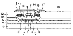
First, a plan view and a cross-sectional view of a structure of a device manufactured by using the manufacturing method according to the first embodiment of the present invention are shown in FIGS. 1 and 2, respectively. The plan view shows one pixel, and the cross-sectional view shows a cross-sectional view taken along a chain line in FIG. The TFT pixel electrode portion is described in detail for the purpose of explaining the gist of the present invention.
[0050]
The manufacturing method will be described below. 19 to 22 are substantially the same as those in the related art. First, as shown in FIG. 19, a
[0051]
Next, B-related ions (mainly B2Hx dimer ions) for adjusting the threshold voltage of the n-type TFT are accelerated at an energy of 20 keV and a dose by an ion doping method (an impurity implantation method that does not select an ion type) over the entire surface of the transparent insulating
[0052]
Then, after removing the photoresist pattern used as the mask for ion doping, the
[0053]
Thereafter, as shown in FIG. 20, an
[0054]
The reason is that when the covering property of the insulating film or the conductor film is improved, cracks due to stress concentration and thin film portions due to insufficient covering are reduced. As a result, for example, in the case of a gate insulating film, the electric withstand voltage is improved, and in the case of a gate conductor film, for example, the probability of disconnection is reduced, and the characteristics and reliability of the element are improved.
[0055]
Thereafter, as shown in FIG. 21, a
[0056]
Then, using the photoresist pattern formed by the photolithography process as a mask, the
[0057]
Next, using the photoresist pattern formed by the photolithography process as a mask, P-related ions are accelerated to the island portion of the n-type TFT portion, that is, the region slightly larger than the
[0058]
Then, using the photoresist pattern formed by the photolithography process and the
[0059]
After that, it is shown in FIGS. First, an
[0060]
Thereafter, the
[0061]
Thereafter, an
[0062]
In the first embodiment of the present invention, an Al film and an ITO film are used for a drain electrode portion (pixel electrode connection portion), a gate electrode terminal connection portion (not shown), and a source / drain electrode terminal connection portion (not shown). Do not directly contact with each other, so that an upper source / drain electrode serving as an intermediate layer is not required above the source /
[0063]
Next, as shown in FIG. 4, an
[0064]
Thereafter, an intermediate electrode film (Mo film) 13 for electrical connection between the source / drain electrode (current electrode) 11 and the
[0065]
The reason is that, for example, in a wet etching process using phosphoric acid, the
[0066]
Thereafter, as shown in FIG. 7, a
[0067]
Thereafter, as shown in FIG. 7, a light transmitting electrode film (ITO film) 16 is deposited to a thickness of 50 nm on the entire surface by sputtering.
[0068]
Then, when the
[0069]
In the manufacturing method of the present invention described above, the
[0070]
That is, since there is no dissolution and disappearance of the
[0071]
Furthermore, since the etching step related to the patterning of the
[0072]
In the liquid crystal display device of the present invention as shown in FIGS. 1 and 2, the
[0073]
More specifically, as shown in FIG. 1, the
[0074]
Further, since a part of the contact surface of the dissimilar material having poor corrosion resistance can be protected from above by the
[0075]
This is because dangling bond defect density due to lattice mismatch etc. is high on the contact surface between different materials and chemical reaction is likely to occur. In addition, when a corrosive environment such as water is interposed, the difference in redox potential between each other is used as driving force. This is because the battery corrosion reaction easily proceeds.
[0076]
Furthermore, in the present invention, since the battery effect does not occur in principle during pixel electrode patterning, the intermediate electrode film and the reflective electrode film can be formed thinner than in the past, so that peeling of the electrode film due to stress can be prevented. , Throughput is improved.
[0077]
Next, a manufacturing method according to a second embodiment of the present invention will be described. 8 and 9 are a plan view and a cross-sectional view of the structure obtained according to the present embodiment. The steps up to FIG. 5 are the same as those in the first embodiment.
[0078]
In this embodiment, as shown in FIG. 10, a
[0079]
Next, by removing the photoresist pattern for patterning the
[0080]
In the present embodiment, in addition to the effects of the first embodiment, the
[0081]
Next, FIGS. 11 and 12 are a plan view and a cross-sectional view of a structure obtained by the method according to the third embodiment of the present invention. The steps up to FIG. 5 are the same as those in the second embodiment.
[0082]
In the present embodiment, as shown in FIG. 13, the
[0083]
Next, by removing the photoresist pattern for patterning the
[0084]
In the present embodiment, since the periphery of the contact surface of the dissimilar material having poor corrosion resistance can be protected from above with the
[0085]
Further, since the
[0086]
FIG. 14 is a cross-sectional view of a structure obtained by the manufacturing method according to the fourth embodiment of the present invention, and FIGS. 15 and 16 show intermediate process drawings. The plan view is omitted. With reference to these drawings, another liquid crystal display device of the present invention and a method of manufacturing the same will be described. The steps up to FIG. 4 are substantially the same as those in the above-described first embodiment, and a description thereof will not be repeated.
[0087]
After the step shown in FIG. 4, as shown in FIG. 15, an
[0088]
Thereafter, a
[0089]
Thereafter, as shown in FIG. 16, a
[0090]
Also in the above method, the
[0091]
As shown in FIG. 14, the
[0092]
FIG. 17 shows a cross-sectional view obtained by the manufacturing method according to the fifth embodiment of the present invention. With reference to these drawings, another liquid crystal display device of the present invention and a method of manufacturing the same will be described. The steps up to FIG. G are substantially the same as those in the first embodiment.
[0093]
After reaching FIG. G, a
[0094]
Next, when the
[0095]
In the structure shown in FIG. 17, the
[0096]
As a result, the electric resistance between the
[0097]
It should be noted that the structure of the pixel electrode is not limited to the U-shaped structure of the reflective electrode portion as used in the above-described example, and it goes without saying that the pixel electrode may be appropriately determined.
[0098]
Al used for the
[0099]
The composition of the Al alloy includes at least one of Sc, Y, Nd, Ti, Zr, Hf, Ta, Cr, Mo, W, Co, Ni, Pd, Cu, and Si. Is preferred.
[0100]
In particular, Sc, Y, Nd, Ti, Zr, Hf, Ta, and Cr have high heat resistance and have an electrode potential close to Al or a base side, so that unexpected local corrosion can be suppressed. It is suitable.
[0101]
Further, it is desirable that the contents of Sc, Y, Nd, Ti, Zr, Hf, Ta, and Cr be 0.5 at% or more and 10 at% or less. In particular, if it is in the range of 0.5 to 5%, heat resistance of 150 ° C. or more, resistivity of 20 μΩ · cm or less, and reflectance of 80% or more can be obtained.
[0102]
Ag may be used instead of Al. The reason is that the visible light reflectance is higher and the resistance is lower than Al.
[0103]
The
[0104]
As the
[0105]
The thickness of the
[0106]
Further, it is desirable that the thickness of only the
[0107]
Further, the structure of the
[0108]
Needless to say, ZnO or the like can be used for the
[0109]
Note that, in the embodiment of the present invention, a case where a p-Si TFT having high mobility is used is illustrated, but the present invention is not limited to this and can be applied to a case where an a-Si TFT is used. Further, the present invention may be applied to a so-called passive matrix type liquid crystal display device using a two-terminal element or using no active element.
[0110]
【The invention's effect】
According to the liquid crystal display device of the present invention, the battery corrosion reaction can be completely prevented. The reason is that the
[0111]
Further, according to the liquid crystal display device of the present invention, external effects (water, oxygen, chemicals, and the like) received from the environment can be blocked, and the corrosion reliability of the contact surface between different materials can be improved. The reason is that a part of the contact surface between different materials having poor corrosion resistance can be protected by the
[0112]
Further, according to the method for manufacturing a liquid crystal display device of the present invention, an etching step relating to patterning of the
[Brief description of the drawings]
FIG. 1 is a plan view of a liquid crystal display device according to a first embodiment of the present invention.
FIG. 2 is a sectional view of the liquid crystal display device according to the first embodiment of the present invention.
FIG. 3 is a diagram showing a manufacturing process according to the first embodiment of the present invention.
FIG. 4 is a diagram illustrating a manufacturing process according to the first embodiment of the present invention.
FIG. 5 is a diagram illustrating a manufacturing process according to the first embodiment of the present invention.
FIG. 6 is a diagram illustrating a manufacturing process according to the first embodiment of the present invention.
FIG. 7 is a diagram illustrating a manufacturing process according to the first embodiment of the present invention.
FIG. 8 is a plan view of a liquid crystal display device according to a second embodiment of the present invention.
FIG. 9 is a sectional view of a liquid crystal display device according to a second embodiment of the present invention.
FIG. 10 is a diagram illustrating a manufacturing process according to a second embodiment of the present invention.
FIG. 11 is a plan view of a liquid crystal display device according to a third embodiment of the present invention.
FIG. 12 is a sectional view of a liquid crystal display device according to a third embodiment of the present invention.
FIG. 13 is a diagram illustrating a manufacturing process according to a third embodiment of the present invention.
FIG. 14 is a sectional view of a liquid crystal display device according to a fourth embodiment of the present invention.
FIG. 15 is a diagram illustrating a manufacturing process according to a fourth embodiment of the present invention.
FIG. 16 is a diagram illustrating a manufacturing process according to a fourth embodiment of the present invention.
FIG. 17 is a sectional view of a liquid crystal display device according to a fifth embodiment of the present invention.
FIG. 18 is a diagram illustrating a manufacturing process according to a fifth embodiment of the present invention.
FIG. 19 is a diagram showing a manufacturing process according to the related art.
FIG. 20 is a diagram showing a manufacturing process according to the related art.
FIG. 21 is a diagram showing a manufacturing process according to the related art.
FIG. 22 is a diagram showing a manufacturing process according to the related art.
FIG. 23 is a diagram showing a manufacturing process of a conventional technique.
FIG. 24 is a diagram showing a manufacturing process according to the related art.
FIG. 25 is a diagram showing a manufacturing process of a conventional technique.
FIG. 26 is a diagram showing a manufacturing process according to the related art.
FIG. 27 is a cross-sectional view of a conventional liquid crystal display device.
[Explanation of symbols]
1 Glass substrate
2 Base SiO2 film
3 p-Si film
4 Interface SiO2 film
5 Gate SiO2 film
6 μc-Si film
7 Gate electrode
8 SD area
9 LDD area
10 Interlayer SiO2 film
11 Source and drain electrodes
12 Interlayer Si3N4 film
13 Intermediate electrode
14 Reflection pixel electrode
15 Photoresist film
16 Transparent pixel electrode
17 Lower source / drain electrodes
18 Upper source / drain electrode
Claims (19)
Priority Applications (1)
| Application Number | Priority Date | Filing Date | Title |
|---|---|---|---|
| JP2002306991A JP2004144826A (en) | 2002-10-22 | 2002-10-22 | Liquid crystal display device and method for manufacturing the same |
Applications Claiming Priority (1)
| Application Number | Priority Date | Filing Date | Title |
|---|---|---|---|
| JP2002306991A JP2004144826A (en) | 2002-10-22 | 2002-10-22 | Liquid crystal display device and method for manufacturing the same |
Publications (1)
| Publication Number | Publication Date |
|---|---|
| JP2004144826A true JP2004144826A (en) | 2004-05-20 |
Family
ID=32453593
Family Applications (1)
| Application Number | Title | Priority Date | Filing Date |
|---|---|---|---|
| JP2002306991A Pending JP2004144826A (en) | 2002-10-22 | 2002-10-22 | Liquid crystal display device and method for manufacturing the same |
Country Status (1)
| Country | Link |
|---|---|
| JP (1) | JP2004144826A (en) |
Cited By (7)
| Publication number | Priority date | Publication date | Assignee | Title |
|---|---|---|---|---|
| JP2007226186A (en) * | 2006-02-20 | 2007-09-06 | Samsung Electronics Co Ltd | Display substrate, manufacturing method thereof, and display device having the same |
| US7570327B2 (en) | 2006-07-19 | 2009-08-04 | Nec Lcd Technologies, Ltd. | Semi-transmissive type liquid-crystal display device and method of fabricating the same |
| JP2009217038A (en) * | 2008-03-11 | 2009-09-24 | Toshiba Mobile Display Co Ltd | Liquid crystal display device |
| EP2506308A1 (en) * | 2011-03-28 | 2012-10-03 | Boe Technology Group Co. Ltd. | Amorphous oxide thin film transistor, method for manufacturing the same, and display panel |
| US8384280B2 (en) | 2007-12-26 | 2013-02-26 | Kobe Steel, Ltd. | Reflective electrode, display device, and method for producing display device |
| US20130256121A1 (en) * | 2012-03-31 | 2013-10-03 | Shenzhen China Star Optoelcetronics Technology Co., Ltd. | Manufacturing method of reflective layer for reflective type liquid crystal |
| US8729794B2 (en) | 2007-06-01 | 2014-05-20 | Japan Display Inc. | Display device having three layer electroconductive film |
-
2002
- 2002-10-22 JP JP2002306991A patent/JP2004144826A/en active Pending
Cited By (10)
| Publication number | Priority date | Publication date | Assignee | Title |
|---|---|---|---|---|
| JP2007226186A (en) * | 2006-02-20 | 2007-09-06 | Samsung Electronics Co Ltd | Display substrate, manufacturing method thereof, and display device having the same |
| US7570327B2 (en) | 2006-07-19 | 2009-08-04 | Nec Lcd Technologies, Ltd. | Semi-transmissive type liquid-crystal display device and method of fabricating the same |
| US8729794B2 (en) | 2007-06-01 | 2014-05-20 | Japan Display Inc. | Display device having three layer electroconductive film |
| US8384280B2 (en) | 2007-12-26 | 2013-02-26 | Kobe Steel, Ltd. | Reflective electrode, display device, and method for producing display device |
| JP2009217038A (en) * | 2008-03-11 | 2009-09-24 | Toshiba Mobile Display Co Ltd | Liquid crystal display device |
| US8405805B2 (en) | 2008-03-11 | 2013-03-26 | Japan Display Central Inc. | Liquid crystal display device |
| EP2506308A1 (en) * | 2011-03-28 | 2012-10-03 | Boe Technology Group Co. Ltd. | Amorphous oxide thin film transistor, method for manufacturing the same, and display panel |
| US9112040B2 (en) | 2011-03-28 | 2015-08-18 | Boe Technology Group Co., Ltd. | Amorphous oxide thin film transistor, method for manufacturing the same, and display panel |
| US9608127B2 (en) | 2011-03-28 | 2017-03-28 | Boe Technology Group Co., Ltd. | Amorphous oxide thin film transistor, method for manufacturing the same, and display panel |
| US20130256121A1 (en) * | 2012-03-31 | 2013-10-03 | Shenzhen China Star Optoelcetronics Technology Co., Ltd. | Manufacturing method of reflective layer for reflective type liquid crystal |
Similar Documents
| Publication | Publication Date | Title |
|---|---|---|
| US6350995B1 (en) | Thin film transistor and manufacturing method therefore | |
| TW200810129A (en) | Active matrix TFT array substrate and method of manufacturing the same | |
| US6395586B1 (en) | Method for fabricating high aperture ratio TFT's and devices formed | |
| KR980012071A (en) | Manufacturing method of thin film transistor | |
| US8199270B2 (en) | TFT-LCD array substrate and method of manufacturing the same | |
| US10833104B2 (en) | Array substrate and its fabricating method, display device | |
| US7479415B2 (en) | Fabrication method of polycrystalline silicon liquid crystal display device | |
| US7833813B2 (en) | Thin film transistor array panel and method of manufacturing the same | |
| CN102236204B (en) | There is transflective liquid crystal display device and the manufacture method thereof of thin film transistor (TFT) | |
| JPH06188265A (en) | Semiconductor device and manufacture thereof | |
| US20240224629A1 (en) | Display panel and manufacturing method thereof, and display device | |
| KR0171648B1 (en) | Thin film device and manufacturing method | |
| JP2004144826A (en) | Liquid crystal display device and method for manufacturing the same | |
| US12100711B2 (en) | Active matrix substrate and method for manufacturing same | |
| JP2006330130A (en) | Liquid crystal display device and manufacturing method thereof | |
| US10529749B2 (en) | Manufacturing method for thin film transistor array substrate | |
| TWI269449B (en) | Photo-electronic display device and the making method thereof | |
| US6160598A (en) | Liquid crystal display and a method for fabricating thereof | |
| US20070273814A1 (en) | Transflective display apparatus and method of manufacturing the same | |
| US10497724B2 (en) | Manufacturing method of a thin film transistor and manufacturing method of an array substrate | |
| JP3200639B2 (en) | Method for manufacturing thin film transistor panel | |
| JP2003156764A (en) | Method of manufacturing thin film transistor array substrate and liquid crystal display device having the same | |
| CN105765709A (en) | Array substrate and manufacturing method thereof, display panel, display device | |
| JP4219717B2 (en) | A display device manufacturing method, a liquid crystal display device, and a metal film patterning method. | |
| CN100456098C (en) | Pixel structure and manufacturing method thereof |
Legal Events
| Date | Code | Title | Description |
|---|---|---|---|
| RD01 | Notification of change of attorney |
Free format text: JAPANESE INTERMEDIATE CODE: A7421 Effective date: 20050309 |
|
| A621 | Written request for application examination |
Free format text: JAPANESE INTERMEDIATE CODE: A621 Effective date: 20050914 |
|
| RD01 | Notification of change of attorney |
Free format text: JAPANESE INTERMEDIATE CODE: A7421 Effective date: 20060120 |
|
| A131 | Notification of reasons for refusal |
Free format text: JAPANESE INTERMEDIATE CODE: A131 Effective date: 20090512 |
|
| A02 | Decision of refusal |
Free format text: JAPANESE INTERMEDIATE CODE: A02 Effective date: 20091007 |