JP2004066543A - Semiconductor laser array light source - Google Patents
Semiconductor laser array light source Download PDFInfo
- Publication number
- JP2004066543A JP2004066543A JP2002226381A JP2002226381A JP2004066543A JP 2004066543 A JP2004066543 A JP 2004066543A JP 2002226381 A JP2002226381 A JP 2002226381A JP 2002226381 A JP2002226381 A JP 2002226381A JP 2004066543 A JP2004066543 A JP 2004066543A
- Authority
- JP
- Japan
- Prior art keywords
- semiconductor laser
- laser array
- light source
- submount
- emission light
- Prior art date
- Legal status (The legal status is an assumption and is not a legal conclusion. Google has not performed a legal analysis and makes no representation as to the accuracy of the status listed.)
- Pending
Links
Images


Landscapes
- Laser Beam Printer (AREA)
- Semiconductor Lasers (AREA)
Abstract
Description
【0001】
【発明の属する技術分野】
本発明は、複数のレーザビームの走査光と電子写真プロセスにより印字するレーザビームプリンタ等に用いられる半導体レーザアレイ光源に関するものである。
【0002】
【従来の技術】
従来、レーザプリンタ等の電子写真方式のデジタル画像形成装置においては、半導体レーザ素子からの光ビームをポリゴンスキャナと呼ばれる回転多面鏡で偏向走査し、これを副走査方向に移動する感光体の被走査面に照射する。光ビームは出力すべき画像に応じて変調されるので、感光体上には出力すべき画像に応じた静電潜像が形成され、この静電潜像が現像されてトナー像となる。このトナー像が記録紙に転写され定着されることにより、記録紙に画像が形成される。
【0003】
このようなデジタル画像形成装置において高速で画像を出力するためには、光ビームの走査速度を高める必要がある。しかし、光ビーム走査速度は回転多面鏡の回転速度の限界によって制限される。そこで近年、複数の光ビームで被走査面を同時に走査するマルチビーム方式が採用されるようになった。この方式によれば、光ビーム数に比例して画像出力速度を高めることがことができる。つまり、感光体に同時に走査する光ビームの本数を2本、3本と増加させていけば、画像出力速度を2倍、3倍と高速化することができる。例えば、特開平5−29711号、特開平11−84283号等では、複数の半導体レーザ素子を副走査方向に配列して半導体レーザアレイを製造し、これを光書込系の光源部に用いた画像形成装置が提案されている。
【0004】
一方、出力画像の精細度を高めるためには、走査線の間隔(ピッチ)を狭くする必要がある。そのためには半導体レーザ素子相互間のピッチを狭くすればよい。しかしながら、半導体レーザ素子相互間のピッチをあまり狭くしすぎると、クロストークやドループが発生する問題が生じる。そこで、半導体レーザ素子相互間のピッチを広くし、半導体レーザアレイを副走査方向に対して傾けて保持すれば、クロストーク等の問題を防止できると共に、半導体レーザ素子相互間の見かけ上の(副走査方向における)ピッチを狭くすることができる。
【0005】
【発明が解決しようとする課題】
しかし、半導体レーザ素子を1列に4個以上配列すると、両端の半導体レーザ素子からの光ビームの間隔がレンズのイメージサークルより大きくなり、収差が生じて光学性能が著しく低下し、画像再現性を劣化させることになる。また、特開平11−249043号記載の複数個の汎用の半導体レーザを用いた構成は組立性が悪く、複雑な走査光学系が必要となるといった問題がある。
【0006】
一方、特開平9−200431号では、複数の面発光レーザ素子を備えた2次元面発光レーザアレイが提案されている。しかしながら、面発光レーザ素子の場合には光出力が1つの光源で最大1mW程度であり、1つの光源で少なくとも5mWである端面発光レーザ素子と比べて光出力が低い。そのため、1次元2ビーム端面発光レーザアレイの場合、2つの光源で10mWの光出力が得られるが、これと同等の光出力を面発光レーザアレイで得るには、少なくとも10個の光源を持つ2×5の2次元面発光レーザアレイとなってしまう。そのため、面発光レーザ素子を用いた場合には、端面発光レーザ素子と比較して駆動装置が複雑になるとともに、光源の発光面積が大きくなるためレンズのイメージサークルが大きくせざるを得ず、記録装置全体のコストが高くなってしまう不具合がある。
【0007】
そこで本発明は、半導体レーザ素子を複数個用いた半導体レーザアレイ光源であって、組立性が良く、安価に製造でき、しかも複雑な走査光学系が不要な半導体レーザアレイ光源を提供することを目的とする。
【0008】
【課題を解決するための手段】
上記目的を達成するため本発明は、サブマウントと、サブマウントの片面に固着され複数個の第1の光ビーム出射光源を有する第1の半導体レーザアレイと、サブマウントの他面に固着され複数個の第2の光ビーム出射光源を有する第2の半導体レーザアレイとを備える半導体レーザアレイ光源を提供する。 かかる構成によれば、2次元光ビーム配列が実現されるため、光ビーム出射光源を一列に並べた場合と比較してレンズのイメージサークルの範囲が小さく抑えられる。また、第1及び第2の半導体レーザアレイがサブマウントの両面に固着されるため、複数個の光ビーム出射光源を容易に精度良く取り付けられる。
【0009】
請求項2の発明は、請求項1記載の半導体レーザアレイ光源において、前記第2の光ビーム光源間の略中央に、前記第1の光ビーム出射光源が設置されていることを特徴としている。また、請求項3の発明は、請求項1記載の半導体レーザアレイ光源において、主走査方向に対する前記サブマウントの傾きをθとし、サブマウントの厚み方向における第1の光ビーム出射光源と第2の光ビーム出射光源との距離をP2としたとき、第1の光ビーム出射光源と第2の光ビーム出射光源のサブマウントの傾き方向における位置ずれZが、P2×tanθであることを特徴としている。これら構成によれば、複数のレーザ出射光源が副走査方向に1列に並ぶ。
【0010】
請求項4の発明は、請求項1乃至3記載の半導体レーザアレイ光源において、窪みが形成されたヒートシンクを更に備え、前記サブマウントはヒートシンクに取りつけられ、前記第2の半導体レーザアレイは当該窪みに収容されていることを特徴としている。かかる構成によれば、半導体レーザアレイの熱がサブマウントを介してヒートシンクに伝わるため、半導体レーザアレイが効率良く冷却される。なお、サブマウントは放熱性の良い材料で形成されているのが好ましい。
【0011】
光ビーム出射光源は端面発光型レーザ素子であることが好ましい。端面発光型レーザ素子は面発光型レーザ素子と比較して光出力が高いため、駆動装置の構成を簡単にできるためである。
【0012】
【発明の実施の形態】
本発明の実施の形態による半導体レーザアレイ光源について図1乃至図4に基づき説明する。
図1は本発明の半導体レーザアレイ光源40を光源部に備える光走査装置100の構成を示す概略図である。まず、光走査装置100の全体構成から説明する。図1に示すように、光走査装置100は半導体レーザアレイ光源40と、コリメータレンズ110と、スキャナモータ115と、非球面レンズ112と、感光体111と、ビーム検出器52とを備える。半導体レーザアレイ光源40は印字データに基づきオン/オフ制御され、後述する4個の端面発光型レーザ素子から4本の光ビームを出射する。スキャナモータ115はポリゴンミラー113と駆動モータ114で構成されており、駆動モータ114はポリゴンミラー113を少ない回転変動で高速回転させる。感光体111は副走査方向に回転する。
【0013】
半導体レーザアレイ光源40より出射した4本の光ビームはコリメータレンズ110を通り、ポリゴンミラー113に達する。ポリゴンミラー113は高速回転しているので4本の光ビームを偏向して走査する。偏向走査された4本のビームは非球面レンズ112を介して感光体111上に達し、主走査方向に走査することにより感光体111の被走査面111aに静電潜像を形成する。この時4本の光ビームの照射位置が副走査方向において特定のピッチ(例えば600dipの画像形成の場合には約40μm)となり、且つ副走査方向において重ならないように、半導体レーザアレイ光源40が固定されている。また、コリメータ110及び非球面レンズ112により感光体111上の光ビームは一定に絞られている。
【0014】
ビーム検出器52は感光体111上の書出位置を決定するものであり、感光体111の近傍位置かつ光ビーム走査上に設けられている。ビーム検出器52には高速型PINホトダイオードが用いられているため、各光ビームの書出位置を決定するのに必要とされる高速応答が可能となっている。
【0015】
次に、半導体レーザアレイ光源40の具体的構成について図2乃至図4を参照して説明する。図2に示すように、半導体レーザアレイ光源40は、第1の半導体レーザアレイ1と、第2の半導体レーザアレイ2と、サブマウント3と、ホトダイオード4と、ステム5と、ヒートシンク6とを備える。サブマウント3はALN等の放熱性の良い材料で形成されていて、両面には半導体レーザアレイ1、2の図示しない電極部に通電するためのパターン、スルーホール穴、パッド部が形成されている(図示せず)。
【0016】
第1の半導体レーザアレイ1はレーザ出射光源(半導体レーザ素子)11、12を備え、合計2本の光ビームを出射することができる。また、第1の半導体レーザアレイ1はレーザ出射光源11、12の共通電極面1aを有し、共通電極面1aと反対の面には図示しない電極部が設けられている。同様に、第2の半導体レーザアレイ2はレーザ出射光源21、22を備え、合計2本の光ビームを出射できる。第2の半導体レーザアレイ2は更にレーザ出射光源21、22の共通電極面2aを有し、共通電極面2aと反対の面には図示しない電極部が設けられている。これら半導体レーザアレイ1、2の電極部はサブマウント3の両面に形成された前記パターンに蒸着半田PbSnを用いて半田つけされ、これにより半導体レーザアレイ1、2がサブマウント3の両側に固着されている。
【0017】
サブマウント3は中央に窪み6aが形成されたヒートシンク6に半田付けやロウ付けなどで固着されている。半導体レーザアレイ2は窪み6aに収容され、その共通電極面2aはヒートシンク6に直接半田付けされている。また、第1の半導体レーザアレイ1の共通電極面1aはAg線8bによりヒートシンク6に接続されている。かかる構成により、半導体レーザアレイ1、2は直接、或いはサブマウント3又はAg線8bを介してヒートシンク6に熱を逃がすことができる。これによって、半導体レーザアレイ1、2の冷却を効率良く行って温度上昇の低減を図ることができ、熱による影響として発生するクロストークやドループの低減が可能となり、半導体レーザアレイ光源40の特性を安定に保つことが可能となる。なお、図3に示すように、半導体レーザアレイ2の側面はヒートシンク6には接触せず、半導体レーザアレイ2とヒートシンク6との間に隙間が設けられている。
【0018】
ステム5には端子71、72、73、74、75、76が設けられていて、端子71乃至75はステム5から電気的絶縁状態に保たれるよう、ガラスなどのハーメチックシール部材でシールされている。端子71、72、74、75はサブマウント3に形成された前記パッド部(図示せず)にAg線8aによりそれぞれ接続されている。ヒートシンク6は、ステム5の前面にロウ付けなどで接合され、端子76と接合している。
【0019】
サブマウント3の後方には、光ビームの強度モニタとしてのホトダイオード4が設けられている。ホトダイオード4の図示しないパッド部は、Ag線8cにより端子73に接続されている。
【0020】
ここで、端子71と76間に電圧が印可され特定の電流が流れると、サブマウント3上のパターンでつながった第1の半導体レーザアレイ1に電流が流れ、レーザ出射光源11より電流に応じた強度の光ビームが出射される。同様に端子72と76間に電圧が印可されると、第1の半導体レーザアレイ1に電流が流れ、レーザ出射光源12より電流に応じた強度の光ビームが出射される。端子74と76間に電圧が印可されると、第2の半導体レーザアレイ2に電流が流れ、レーザ出射光源21より電流に応じた強度の光ビームが出射され、端子75と76間に電圧が印可されると、第2の半導体レーザアレイ2に電流が流れ、レーザ出射光源22より電流に応じた強度の光ビームが出射される。
【0021】
このとき、光ビームは各レーザ出射光源11、12、21、22の光ビーム出射端面から前方に出射されるだけでなく、後方の端面からも出射される。後端面からの光ビームはホトダイオード4に入射し、光強度モニタ信号として外部へ出力される。
【0022】
図3は、半導体レーザアレイ光源40を半導体レーザアレイ1、2の光ビーム出射端面側(前方)から見た図である。レーザ出射光源11、12(21、22)間のピッチP1は100μmであり、サブマウント3の厚さは100μmである。レーザ出射光源11、12、21、22はサブマウント3近傍より出射される(埋め込み型リッジ構造等の場合)ので、サブマウント3の厚さ方向におけるレーザ出射光源11、21間のピッチP2もほぼ100μmである。
【0023】
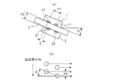
次に、本実施の形態における半導体レーザアレイ1、2の配置関係と感光体111上を走査する光ビームの位置関係について説明する。図4(a)において、半導体レーザアレイ光源40はサブマウント3が水平方向H(主走査方向)に対し特定の角度θ傾けて配置されている。また、サブマウント3の傾き方向におけるレーザ出射光源12と21との位置ずれZは、ほぼゼロの値となるよう配置されている。これにより図4(b)に示す光ビームの感光体111上における副走査方向におけるピッチP3は、600dpi(約42.3μm)で等間隔となる。従って、2次元面で配列された光ビームを用いて4本の走査線を同時に走査することが可能であり、高速、高精細の書込みが可能になる。
【0024】
次に、本発明の実施の形態の変型例について説明する。ここでは図5(a)に示すように位置ずれ量ZがピッチP2×tanθ近傍の値となるように設定することで、レーザ出射光源11と22を副走査方向に一列に並べている。その結果、図5(b)に示すようにレーザ出射光源11と22からの光ビームの感光体111上の入射位置も副走査方向に一列に並ぶ。レーザ出射光源12と21に付いても同様である。このような配置により以下の問題点を解決できる。
【0025】
つまり、前述の実施の形態においてはレーザ出射光源11と22から出射された光ビームが主走査方向で非常に隣接しているため、ビーム検出器52のディテクタ部(図示せず)に複数の光ビームが重なって入射してしまい、これらの光ビームを分離することが困難である。これはレーザ出射光源12と21の場合も同様である。また、傾き角θの値を大きくすれば、光ビームの主走査方向の間隔がますます狭くなり、4本すべての光ビームを分離検出することが出来なくなる。光ビームを分離検出できなければ書出信号が得られず、感光体111上に光を発光させるタイミングが解らなくなり、印刷不可能になってしまう。
【0026】
しかしながら、本例の様にレーザ出射光源11と22を副走査方向に一列に並べれば、レーザ出射光源11と22からの光ビームがビーム検出器52へは同時に入射するため、書出位置を容易に決定することが可能となる。レーザ出射光源12と21についても同様である。
【0027】
また、図6(a)示すように傾き角θを90°とし、レーザ出射光源11と12、レーザ出射光源21と22を副走査方向に並べることもできる。この場合、レーザ出射光源22がレーザ出射光源11、12間の略中央に位置するように位置ずれ量Z=P1/2と設定すれば、図6(b)に示すように感光体111上のピッチP3を均一にできる。なお、位置ずれ量Zの値は数1で求められる。
Z=P3/N ・・・・・・ (数1)
Nは光学系の倍率である。
【0028】
このように、2個の半導体レーザアレイ1、2でサブマウント3を挟み込むように設置することで4本の光ビームを2次元で出射可能なレーザ光源を実現でき、コリメータレンズ110のイメージサークルのエリアを4本のレーザ出射光源を1列に並べた場合(300μmとなる)よりも大幅に小さくすることができる。従って、コリメータレンズ110の小型化が図られ、安価な光走査装置100を提供することができる。
【0029】
更に、レーザ出射光源11、12、21、22は端面発光型レーザ素子であるため、半導体レーザアレイ光源40を駆動するための駆動装置の構成を簡単にできる。また、面発光型レーザ素子を使用した場合に比べてコリメータレンズ110のイメージサークルのエリアを更に小さくできると共に、少ないレーザ出射光源で高い光出力を得ることができる。
【0030】
本発明による半導体レーザアレイ光源は上述した実施の形態に限定されず、特許請求の範囲に記載した範囲で種々の変形や改良が可能である。例えば、前記実施の形態では2本の光ビームを発生する半導体レーザアレイを用いたが、2本以上光ビームを発生する半導体レーザアレイを用いても同様の効果が得られる。また、光ビームを隣接走査したときの場合について説明したが、飛び越し走査の場合も同様の効果が得られる。なお、飛び越し走査については周知であるため説明は省略する。
【0031】
【発明の効果】
請求項1記載の半導体レーザアレイ光源によれば、レンズのイメージサークルの範囲を小さく抑えられるので、収差による光学性能の低下といった問題を回避して光学系の性能を確保することができると共に、レンズの小型化と低価格化が可能になる。また、複数個の光ビーム出射光源を容易に精度良く取り付けられるので、製造工程を簡易にできる。
【0032】
請求項2及び3記載の半導体レーザアレイ光源によれば、複数のレーザ出射光源が副走査方向に一列並ぶので、感光体上の書出位置を確実に決定でき、印刷が可能になる。
【0033】
請求項4記載の半導体レーザアレイ光源によれば、サブマウントを介して半導体レーザアレイが効率良く冷却されるので、クロストークやドループの改善を図ることができ、半導体レーザの性能を向上できる。また、サブマウントを放熱性の良い材料で形成すれば、より効率よく冷却を行うことができる。
【図面の簡単な説明】
【図1】本発明の実施の形態による半導体レーザアレイ光源を光源部に用いた光走査装置の一例を示す構成図。
【図2】半導体レーザアレイ光源の概略構成図。
【図3】光ビーム出射端面から見た半導体レーザアレイ光源の一部拡大図。
【図4】(a)は2個の半導体レーザアレイの配置関係を示す平面図であり、(b)は感光体上を走査する光ビームの位置関係を示す平面図。
【図5】第1の変型例を示す図であり、(a)2個の半導体レーザアレイの配置関係を、(b)は感光体上を走査する光ビームの位置関係を示す平面図。
【図6】第2の変型例を示す図であり、(a)2個の半導体レーザアレイの配置関係を、(b)は感光体上を走査する光ビームの位置関係を示す平面図。
【符号の説明】
1、2.....半導体レーザアレイ、 3.....サブマウント、 6.....ヒートシンク、 11、12、21、22.....レーザ出射光源、 40.....半導体レーザアレイ光源、 52.....ビーム検出器、 110.....コリメータレンズ、 112.....非球面レンズ、 113.....ポリゴンミラー、 111.....感光体[0001]
TECHNICAL FIELD OF THE INVENTION
The present invention relates to a semiconductor laser array light source used for a laser beam printer or the like for performing printing by scanning light of a plurality of laser beams and an electrophotographic process.
[0002]
[Prior art]
2. Description of the Related Art Conventionally, in an electrophotographic digital image forming apparatus such as a laser printer, a light beam from a semiconductor laser element is deflected and scanned by a rotating polygon mirror called a polygon scanner, and this is scanned by a photosensitive member moving in a sub-scanning direction. Irradiate the surface. Since the light beam is modulated according to the image to be output, an electrostatic latent image corresponding to the image to be output is formed on the photoconductor, and this electrostatic latent image is developed into a toner image. The toner image is transferred to the recording paper and fixed, whereby an image is formed on the recording paper.
[0003]
In order to output an image at high speed in such a digital image forming apparatus, it is necessary to increase the scanning speed of the light beam. However, the light beam scanning speed is limited by the rotation speed limit of the rotary polygon mirror. Therefore, in recent years, a multi-beam system for simultaneously scanning a surface to be scanned with a plurality of light beams has been adopted. According to this method, the image output speed can be increased in proportion to the number of light beams. That is, if the number of light beams that scan the photoconductor simultaneously is increased to two or three, the image output speed can be increased to twice or three times. For example, in JP-A-5-29711 and JP-A-11-84283, a semiconductor laser array is manufactured by arranging a plurality of semiconductor laser elements in the sub-scanning direction, and this is used for a light source unit of an optical writing system. An image forming apparatus has been proposed.
[0004]
On the other hand, in order to increase the definition of an output image, it is necessary to reduce the interval (pitch) between scanning lines. For this purpose, the pitch between the semiconductor laser elements may be reduced. However, if the pitch between the semiconductor laser elements is made too narrow, there arises a problem that crosstalk and droop occur. Therefore, if the pitch between the semiconductor laser elements is widened and the semiconductor laser array is held at an angle to the sub-scanning direction, problems such as crosstalk can be prevented, and the apparent (sub-) The pitch (in the scanning direction) can be reduced.
[0005]
[Problems to be solved by the invention]
However, when four or more semiconductor laser elements are arranged in one row, the distance between the light beams from the semiconductor laser elements at both ends becomes larger than the image circle of the lens, causing aberrations and significantly lowering the optical performance, thereby reducing image reproducibility. It will deteriorate. In addition, the configuration using a plurality of general-purpose semiconductor lasers described in Japanese Patent Application Laid-Open No. H11-290443 has a problem that the assemblability is poor and a complicated scanning optical system is required.
[0006]
On the other hand, Japanese Patent Application Laid-Open No. Hei 9-200431 proposes a two-dimensional surface emitting laser array including a plurality of surface emitting laser elements. However, in the case of the surface emitting laser element, the light output is about 1 mW at maximum with one light source, and the light output is lower than that of the edge emitting laser element with at least 5 mW with one light source. Therefore, in the case of a one-dimensional two-beam edge emitting laser array, an optical output of 10 mW can be obtained with two light sources, but in order to obtain an equivalent optical output with the surface emitting laser array, at least ten light sources having two light sources are required. The result is a × 5 two-dimensional surface emitting laser array. Therefore, when the surface emitting laser element is used, the driving device becomes more complicated than the edge emitting laser element, and the light emitting area of the light source increases, so that the image circle of the lens has to be enlarged, and the recording is performed. There is a problem that the cost of the entire apparatus increases.
[0007]
Accordingly, an object of the present invention is to provide a semiconductor laser array light source using a plurality of semiconductor laser elements, which has good assemblability, can be manufactured at low cost, and does not require a complicated scanning optical system. And
[0008]
[Means for Solving the Problems]
In order to achieve the above object, the present invention provides a submount, a first semiconductor laser array having a plurality of first light beam emission light sources fixed to one surface of the submount, and a plurality of first semiconductor laser arrays fixed to the other surface of the submount. And a second semiconductor laser array having a plurality of second light beam emission light sources. According to such a configuration, a two-dimensional light beam arrangement is realized, so that the range of the image circle of the lens can be suppressed smaller than when the light beam emission light sources are arranged in a line. Further, since the first and second semiconductor laser arrays are fixed to both surfaces of the submount, a plurality of light beam emission light sources can be easily and accurately attached.
[0009]
According to a second aspect of the present invention, in the semiconductor laser array light source according to the first aspect, the first light beam emitting light source is provided substantially at the center between the second light beam light sources. According to a third aspect of the present invention, in the semiconductor laser array light source according to the first aspect, the inclination of the submount with respect to the main scanning direction is θ, and the first light beam emitting light source and the second light source in the thickness direction of the submount are provided. When the distance between the first light beam emitting light source and the second light beam emitting light source is P2, the displacement Z in the tilt direction of the submount between the first light beam emitting light source and the second light beam emitting light source is P2 × tan θ. . According to these configurations, a plurality of laser emission light sources are arranged in a line in the sub-scanning direction.
[0010]
According to a fourth aspect of the present invention, in the semiconductor laser array light source according to any one of the first to third aspects, a heat sink having a depression is further provided, the submount is attached to the heat sink, and the second semiconductor laser array is disposed in the depression. It is characterized by being housed. According to such a configuration, since the heat of the semiconductor laser array is transmitted to the heat sink via the submount, the semiconductor laser array is efficiently cooled. Preferably, the submount is formed of a material having good heat dissipation.
[0011]
The light beam emission light source is preferably an edge-emitting laser element. This is because the edge-emitting laser element has a higher light output than the surface-emitting laser element, so that the configuration of the driving device can be simplified.
[0012]
BEST MODE FOR CARRYING OUT THE INVENTION
A semiconductor laser array light source according to an embodiment of the present invention will be described with reference to FIGS.
FIG. 1 is a schematic diagram showing a configuration of an
[0013]
The four light beams emitted from the semiconductor laser array
[0014]
The
[0015]
Next, a specific configuration of the semiconductor laser array
[0016]
The first
[0017]
The
[0018]
[0019]
Behind the
[0020]
Here, when a voltage is applied between the
[0021]
At this time, the light beam is emitted not only forward from the light beam emission end faces of the laser
[0022]
FIG. 3 is a diagram of the semiconductor laser array
[0023]
Next, the positional relationship between the
[0024]
Next, a modified example of the embodiment of the present invention will be described. Here, as shown in FIG. 5A, the laser
[0025]
That is, in the above-described embodiment, since the light beams emitted from the laser
[0026]
However, if the laser
[0027]
Further, as shown in FIG. 6A, the laser
Z = P3 / N (Equation 1)
N is the magnification of the optical system.
[0028]
In this manner, a laser light source capable of two-dimensionally emitting four light beams can be realized by placing the
[0029]
Further, since the laser
[0030]
The semiconductor laser array light source according to the present invention is not limited to the above embodiment, and various modifications and improvements can be made within the scope described in the claims. For example, in the above embodiment, a semiconductor laser array that generates two light beams is used, but the same effect can be obtained by using a semiconductor laser array that generates two or more light beams. Also, the case where the light beam is scanned adjacently has been described, but the same effect can be obtained in the case of interlaced scanning. Since the interlaced scanning is well known, the description is omitted.
[0031]
【The invention's effect】
According to the semiconductor laser array light source of the first aspect, the range of the image circle of the lens can be suppressed to be small, so that the problem of a decrease in optical performance due to aberration can be avoided, and the performance of the optical system can be ensured. It is possible to reduce the size and cost of the device. In addition, since a plurality of light beam emission light sources can be easily and accurately attached, the manufacturing process can be simplified.
[0032]
According to the semiconductor laser array light source according to the second and third aspects, the plurality of laser emission light sources are arranged in a line in the sub-scanning direction, so that the writing position on the photosensitive member can be reliably determined and printing can be performed.
[0033]
According to the semiconductor laser array light source of the fourth aspect, since the semiconductor laser array is efficiently cooled via the submount, crosstalk and droop can be improved, and the performance of the semiconductor laser can be improved. If the submount is formed of a material having good heat dissipation, cooling can be performed more efficiently.
[Brief description of the drawings]
FIG. 1 is a configuration diagram showing an example of an optical scanning device using a semiconductor laser array light source according to an embodiment of the present invention in a light source unit.
FIG. 2 is a schematic configuration diagram of a semiconductor laser array light source.
FIG. 3 is a partially enlarged view of a semiconductor laser array light source viewed from a light beam emission end face.
FIG. 4A is a plan view showing an arrangement relationship between two semiconductor laser arrays, and FIG. 4B is a plan view showing a positional relationship of a light beam that scans a photoconductor.
FIGS. 5A and 5B are diagrams showing a first modified example, wherein FIG. 5A is a plan view showing an arrangement relationship between two semiconductor laser arrays, and FIG.
FIGS. 6A and 6B are diagrams showing a second modified example, in which FIG. 6A is a plan view showing an arrangement relationship between two semiconductor laser arrays, and FIG. 6B is a plan view showing a positional relationship of a light beam that scans a photoconductor.
[Explanation of symbols]
1,2. . . . . 2. a semiconductor laser array; . . . . 5. submount, . . . . Heat sinks 11, 12, 21, 22. . . . . Laser emission light source, 40. . . . . Semiconductor laser array light source, 52. . . . . Beam detector, 110. . . . . A collimator lens, 112. . . . . Aspherical lens, 113. . . . . Polygon mirror, 111. . . . . Photoconductor
Claims (4)
Priority Applications (1)
| Application Number | Priority Date | Filing Date | Title |
|---|---|---|---|
| JP2002226381A JP2004066543A (en) | 2002-08-02 | 2002-08-02 | Semiconductor laser array light source |
Applications Claiming Priority (1)
| Application Number | Priority Date | Filing Date | Title |
|---|---|---|---|
| JP2002226381A JP2004066543A (en) | 2002-08-02 | 2002-08-02 | Semiconductor laser array light source |
Publications (1)
| Publication Number | Publication Date |
|---|---|
| JP2004066543A true JP2004066543A (en) | 2004-03-04 |
Family
ID=32013742
Family Applications (1)
| Application Number | Title | Priority Date | Filing Date |
|---|---|---|---|
| JP2002226381A Pending JP2004066543A (en) | 2002-08-02 | 2002-08-02 | Semiconductor laser array light source |
Country Status (1)
| Country | Link |
|---|---|
| JP (1) | JP2004066543A (en) |
Cited By (8)
| Publication number | Priority date | Publication date | Assignee | Title |
|---|---|---|---|---|
| WO2008010966A3 (en) * | 2006-07-18 | 2008-06-19 | Coherent Inc | High power and high brightness diode-laser array for material processing applications |
| JP2010226078A (en) * | 2009-02-24 | 2010-10-07 | Sony Corp | Light emitting device and manufacturing method thereof |
| JP2019192915A (en) * | 2018-04-28 | 2019-10-31 | エスゼット ディージェイアイ テクノロジー カンパニー リミテッドSz Dji Technology Co.,Ltd | Semiconductor apparatus |
| JP2019204890A (en) * | 2018-05-24 | 2019-11-28 | 日本ルメンタム株式会社 | Optical assembly |
| US20220360039A1 (en) * | 2019-09-30 | 2022-11-10 | Osram Opto Semiconductors Gmbh | Laser package and system with laser packages |
| US11902714B1 (en) | 2020-12-20 | 2024-02-13 | Lumus Ltd. | Image projector with laser scanning over spatial light modulator |
| US12326574B2 (en) | 2017-12-10 | 2025-06-10 | Lumus Ltd. | Image projector |
| US12392874B2 (en) | 2018-04-28 | 2025-08-19 | SZ DJI Technology Co., Ltd. | Light detection and ranging sensors with multiple emitters and multiple receivers, and associated systems and methods |
-
2002
- 2002-08-02 JP JP2002226381A patent/JP2004066543A/en active Pending
Cited By (13)
| Publication number | Priority date | Publication date | Assignee | Title |
|---|---|---|---|---|
| US7515346B2 (en) | 2006-07-18 | 2009-04-07 | Coherent, Inc. | High power and high brightness diode-laser array for material processing applications |
| US7697207B2 (en) | 2006-07-18 | 2010-04-13 | Coherent, Inc. | High power and high brightness diode-laser array for material processing applications |
| WO2008010966A3 (en) * | 2006-07-18 | 2008-06-19 | Coherent Inc | High power and high brightness diode-laser array for material processing applications |
| JP2010226078A (en) * | 2009-02-24 | 2010-10-07 | Sony Corp | Light emitting device and manufacturing method thereof |
| US8654810B2 (en) | 2009-02-24 | 2014-02-18 | Sony Corporation | Light-emitting device and method of manufacturing the same |
| US12326574B2 (en) | 2017-12-10 | 2025-06-10 | Lumus Ltd. | Image projector |
| JP2019192915A (en) * | 2018-04-28 | 2019-10-31 | エスゼット ディージェイアイ テクノロジー カンパニー リミテッドSz Dji Technology Co.,Ltd | Semiconductor apparatus |
| US12392874B2 (en) | 2018-04-28 | 2025-08-19 | SZ DJI Technology Co., Ltd. | Light detection and ranging sensors with multiple emitters and multiple receivers, and associated systems and methods |
| JP2019204890A (en) * | 2018-05-24 | 2019-11-28 | 日本ルメンタム株式会社 | Optical assembly |
| JP7132747B2 (en) | 2018-05-24 | 2022-09-07 | 日本ルメンタム株式会社 | optical subassembly |
| JP2022549941A (en) * | 2019-09-30 | 2022-11-29 | エイエムエス-オスラム インターナショナル ゲーエムベーハー | Laser packages and systems with laser packages |
| US20220360039A1 (en) * | 2019-09-30 | 2022-11-10 | Osram Opto Semiconductors Gmbh | Laser package and system with laser packages |
| US11902714B1 (en) | 2020-12-20 | 2024-02-13 | Lumus Ltd. | Image projector with laser scanning over spatial light modulator |
Similar Documents
| Publication | Publication Date | Title |
|---|---|---|
| JP3645598B2 (en) | Multi-beam diode laser array and laser printer using the same | |
| US6798438B2 (en) | Image-recording device for a printing form, having an array of VCSEL light sources | |
| JP2008268721A (en) | Optical scanning apparatus and image forming apparatus | |
| US5640188A (en) | Multiple diode laser employing mating substrates | |
| JPH05294005A (en) | Image forming device | |
| US5432535A (en) | Method and apparatus for fabrication of multibeam lasers | |
| JPH10153742A (en) | Multiple beam light source device | |
| JP5321915B2 (en) | Light source device, optical scanning device, and image forming apparatus | |
| JP2005317925A (en) | Light source device, recording device, plate making device, and image forming device | |
| JP2008192780A (en) | Surface emitting laser module, optical scanning device, image forming apparatus, optical transmission module, and optical transmission system | |
| JP2004066543A (en) | Semiconductor laser array light source | |
| JP2000105347A (en) | Multibeam light source device, multibeam scanning device and image forming device | |
| US6740869B2 (en) | Light beam scanning device for micro-area light source | |
| JP2014157873A (en) | Lid for optical package, optical package, optical unit, multi-beam scanner, and image forming apparatus | |
| KR100538250B1 (en) | Multi-beam emitting device and light scanning unit employing the same | |
| JP2002026445A (en) | Light source device | |
| JP6379755B2 (en) | Light source module, optical scanning device, image forming apparatus, and light source module manufacturing method | |
| JP2004013021A (en) | Light source device, light source module, optical scanning device, and image forming device | |
| JPH10282440A (en) | Optical scanning device and electrophotographic recording device | |
| JP4157647B2 (en) | Multi-beam scanning device and light source device thereof | |
| JP6478146B2 (en) | Light source module and light source module manufacturing method | |
| US6867796B1 (en) | Semiconductor laser array and optical scanner | |
| JP5471278B2 (en) | Optical device, optical scanning apparatus, image forming apparatus, optical transmission module, and optical transmission system | |
| JP3093439B2 (en) | Semiconductor light emitting device | |
| JP2005305950A (en) | Multi-beam laser light source device and multi-beam scanning optical device |
Legal Events
| Date | Code | Title | Description |
|---|---|---|---|
| A521 | Written amendment |
Free format text: JAPANESE INTERMEDIATE CODE: A821 Effective date: 20050121 |
|
| RD04 | Notification of resignation of power of attorney |
Free format text: JAPANESE INTERMEDIATE CODE: A7424 Effective date: 20050121 |
|
| A621 | Written request for application examination |
Free format text: JAPANESE INTERMEDIATE CODE: A621 Effective date: 20050304 |
|
| A131 | Notification of reasons for refusal |
Free format text: JAPANESE INTERMEDIATE CODE: A131 Effective date: 20080806 |
|
| A711 | Notification of change in applicant |
Free format text: JAPANESE INTERMEDIATE CODE: A712 Effective date: 20081028 |
|
| A02 | Decision of refusal |
Free format text: JAPANESE INTERMEDIATE CODE: A02 Effective date: 20090113 |