JP2004023424A - Power amplifier module - Google Patents
Power amplifier module Download PDFInfo
- Publication number
- JP2004023424A JP2004023424A JP2002175501A JP2002175501A JP2004023424A JP 2004023424 A JP2004023424 A JP 2004023424A JP 2002175501 A JP2002175501 A JP 2002175501A JP 2002175501 A JP2002175501 A JP 2002175501A JP 2004023424 A JP2004023424 A JP 2004023424A
- Authority
- JP
- Japan
- Prior art keywords
- power amplification
- inductor
- capacitor
- resonance circuit
- power
- Prior art date
- Legal status (The legal status is an assumption and is not a legal conclusion. Google has not performed a legal analysis and makes no representation as to the accuracy of the status listed.)
- Pending
Links
- 239000003990 capacitor Substances 0.000 claims abstract description 49
- 230000003321 amplification Effects 0.000 claims description 76
- 238000003199 nucleic acid amplification method Methods 0.000 claims description 76
- 230000000903 blocking effect Effects 0.000 claims description 3
- 230000005540 biological transmission Effects 0.000 description 10
- 239000004020 conductor Substances 0.000 description 7
- 238000010586 diagram Methods 0.000 description 7
- 238000013459 approach Methods 0.000 description 2
- 230000000694 effects Effects 0.000 description 2
- 239000002902 ferrimagnetic material Substances 0.000 description 2
- 230000001771 impaired effect Effects 0.000 description 2
- 230000005291 magnetic effect Effects 0.000 description 1
- 238000000034 method Methods 0.000 description 1
Images


Landscapes
- Amplifiers (AREA)
Abstract
Description
【0001】
【発明の属する技術分野】
本発明は、高周波回路等に用いられる電力増幅モジュールに関する。
【0002】
【従来の技術】
現在使用されているデジタル式携帯電話として、例えば、CDMA方式のデジタル式携帯電話がある。このCDMA(Code Division Multiple Access)方式のデジタル式携帯電話は、送信回路の後段に電力増幅モジュールが備えられ、電力増幅モジュールの後段には、送信アンテナが備えられている。この電力増幅モジュールは、線形の電力増幅回路を含んでいる。
【0003】
携帯電話に備えられた送信アンテナは、そのインピーダンスが大きく変化するので、電力増幅モジュールに含まれる電力増幅回路と送信アンテナとを直接接続した場合には、両者のインピーダンスの不整合により反射波が生じ、電力増幅回路の信号が歪んでしまう。この歪みが大きくなると、線形性が損なわれ、信号の復調が困難になる。
【0004】
そこで、従来の電力増幅モジュールでは、送信アンテナと電力増幅回路との間にアイソレータを備え、電力増幅回路が、送信アンテナのインピーダンス変化の影響を受けないようにしてある。
【0005】
ところで、アイソレータを備える電力増幅モジュールにおいて、使用周波数帯域内における電力増幅回路の出力端子に接続される回路のインピーダンス(アイソレータ側インピーダンス)は、VSWR(電圧定在波比)が大きくなると、電力増幅回路の出力インピーダンスに対する不整合の程度が大きくなり、隣接チャネル漏洩電力比が増大し、高周波出力及び電力効率が低下し、電力増幅回路の信号の線形性が損なわれるという問題が生じる。
【0006】
ところが、従来の電力増幅モジュールにおいて、アイソレータ側インピーダンスは、VSWRが小さな値、例えば、VSWR≦1.2となる周波数範囲が極めて狭く、使用周波数帯域の大部分において、VSWRが大きな値となっていた。具体的には、従来の電力増幅モジュールにおいて、アイソレータ側インピーダンスがVSWR≦1.2となる周波数範囲は、使用周波数帯域の2〜3%程度であった。
【0007】
このため、従来の電力増幅モジュールは、電力増幅回路の出力インピーダンスと、アイソレータ側インピーダンスとが不整合になり、隣接チャネル漏洩電力比が増大し、高周波出力及び電力効率が低下し、電力増幅回路の信号の線形性が損なわれるという問題を生じていた。
【0008】
アイソレータ側インピーダンスを調整する部品を新たに追加すれば、使用周波数帯域の広い範囲において、VSWR≦1.2となるように調整することは可能である。しかし、この場合は、部品点数の増大を招き、小型化が妨げられるとともに、コストが高くなるという問題点を生じる。
【0009】
【発明が解決しようとする課題】
本発明の課題は、小型化、低コスト化を図り得る電力増幅モジュールを提供することである。
【0010】
本発明のもう1つの課題は、使用周波数帯域内の広い周波数において、隣接チャネル漏洩電力比の増大、並びに、高周波出力及び電力効率の低下を防ぐことができる電力増幅モジュールを提供することである。
【0011】
本発明の更にもう1つの課題は、使用周波数帯域内の広い周波数において、電力増幅部の信号の線形性を保つことができる電力増幅モジュールを提供することである。
【0012】
【課題を解決するための手段】
上述した課題を解決するため、本発明に係る電力増幅モジュールは、電力増幅部と、コンデンサと、方向性結合器と、アイソレータとを含む。
【0013】
電力増幅部は、入力された信号を増幅して出力する。コンデンサは、電力増幅部の出力ラインに直列に接続される。方向性結合器は、第1のインダクタと、第2のインダクタとを含み、第1のインダクタがコンデンサの後段に備えられ、第2のインダクタが第1のインダクタに結合される。第1のインダクタ及びコンデンサは、LC直列共振回路を構成する。アイソレータは、入力回路が等価的にLC並列共振回路を構成し、第1のインダクタの後段に備えられる。LC直列共振回路の共振周波数、及び、LC並列共振回路の反共振周波数は、使用周波数帯域内にある。
【0014】
上述したように、本発明に係る電力増幅モジュールは、電力増幅部を含んでおり、電力増幅部は、入力された信号を増幅して出力する。このため、例えば、携帯電話の送信回路から出力された信号を増幅できる。
【0015】
本発明に係る電力増幅モジュールは、アイソレータを含んでおり、アイソレータは第1のインダクタの後段に備えられ、第1のインダクタは、電力増幅部の後段に備えられている。このため、アイソレータの後段に備えられる電子機器、例えば、送信アンテナ等は、アイソレータを介して、電力増幅部に接続されることになる。このため、電力増幅部が、送信アンテナ等のインピーダンス変化の影響を受けなくなる。
【0016】
本発明に係る電力増幅モジュールは、コンデンサを含んでおり、コンデンサは、電力増幅部の出力ラインに直列に接続されているので、電力増幅部から出力された信号の直流成分を除去することができ、直流阻止コンデンサとして機能させることができる。
【0017】
また、本発明に係る電力増幅モジュールは、方向性結合器を含んでおり、方向性結合器は、第1のインダクタと、第2のインダクタとを含む。第1のインダクタは、コンデンサの後段に備えられているので、コンデンサから信号が入力される。
【0018】
第2のインダクタは、第1のインダクタに結合されている。このため、第2のインダクタを用いて、コンデンサから入力された信号を検出することにより、電力増幅部とアイソレータとの間の進行波を検出することができる。更に具体的には、この第2のインダクタで検出された信号は、制御部に供給され、制御部から出力される信号により、電力増幅部がコントロールされる。
【0019】
第1のインダクタは、コンデンサの後段に備えられているので、第1のインダクタ及びコンデンサが、LC直列共振回路を構成する。アイソレータは、入力回路が等価的にLC並列共振回路を構成する。
【0020】
アイソレータの入力回路は、第1のインダクタの後段に備えられているから、電力増幅部とコンデンサとの接続点から、コンデンサ側を見たインピーダンス(以下、共振回路側インピーダンスと称する)が、LC直列共振回路とLC並列共振回路との合成インピーダンスになる。
【0021】
このため、LC直列共振回路又はLC並列共振回路の共振条件を用いて、共振回路側インピーダンスを定めることが可能になる。具体的には、LC直列共振回路の共振周波数f0、及び、LC並列共振回路の反共振周波数f1を使用周波数帯域内に設定することにより、使用周波数帯域内の広い周波数において、共振回路側インピーダンスが50Ω整合に近づき小さなVSWRとなるように、例えば、VSWR≦1.2となるように設定することができ、これにより、共振回路側インピーダンスを電力増幅部10の出力インピーダンスに整合させることができる。
【0022】
したがって、共振回路側インピーダンスを電力増幅部10の出力インピーダンスに整合できる結果、使用周波数帯域内の広い周波数において、隣接チャネル漏洩電力比の増大、並びに、高周波出力及び電力効率の低下を防ぐことができる。
【0023】
また、同様に、共振回路側インピーダンスを電力増幅部10の出力インピーダンスに整合できる結果、使用周波数帯域内の広い周波数において、電力増幅部の信号の線形性を保つことができる。
【0024】
更に、本発明に係る電力増幅モジュールにおいて、LC直列共振回路は、既存の方向性結合器及びコンデンサを用いて構成されている。従って、VSWR≦1.2を満たすにあたり、共振回路側インピーダンスを調整するための新たな部品を追加する必要がないので、小型化、低コスト化を図り得る。
【0025】
【発明の実施の形態】
図1は本発明に係る電力増幅モジュールの一実施例を含むブロック図、図2は、図1に示した電力増幅モジュールの一部を更に詳細に示す等価回路図である。図1において、本実施例に係る電力増幅モジュールは、電力増幅部10と、コンデンサCdと、方向性結合器20と、制御部60と、アイソレータ30とを含み、携帯電話の送信回路50と、送信アンテナ40との間に備えられている。
【0026】
電力増幅部10は、例えば、1パッケージ化されたパワーアンプ用のMMIC(Microwave Monolithic IC)であり、電力増幅回路110と、インピーダンス整合回路120とを含む。インピーダンス整合回路120は、電力増幅回路110の後段に備えられ、出力インピーダンスが、例えば、50Ωである。コンデンサCdは、電力増幅部10の出力ラインに直列に接続されている。
【0027】
方向性結合器20は、第1のインダクタL1と、第2のインダクタL2とを含む。第1のインダクタL1及び第2のインダクタL2は、ストリップライン、マイクロストリップライン等の線路で構成されている。
【0028】
第1のインダクタL1は、コンデンサCdの後段に備えられている。第2のインダクタL2は、第1のインダクタL1に結合されている。
【0029】
制御部60は、第2のインダクタL2と電力増幅部10との間に備えられている。コンデンサCd及び第1のインダクタL1は、LC直列共振回路210を構成している。本実施例において、LC直列共振回路210は、等価的にLC直列共振回路を構成するものであれば、コンデンサCd、第1のインダクタL1以外の回路要素を含むものであってもよい。
【0030】
アイソレータ30の入力回路は、中心導体Ls1及びコンデンサC1が並列に接続されてなり、等価的にLC並列共振回路310を構成している。本実施例においては、LC並列共振回路310のキャパシタンス成分C1は、コンデンサCdのキャパシタンスと略一致し、LC並列共振回路310のインダクタンス成分Ls1は、第1のインダクタL1のインダクタンスと略一致している。この入力回路は、第1のインダクタL1の後段に備えられている。
【0031】
本実施例において、LC並列共振回路310は、等価的にLC並列共振回路を構成するものであれば、中心導体Ls1、コンデンサC1以外の回路要素を含むものであってもよい。
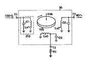
【0032】
図2は、アイソレータ30を更に詳細に示す等価回路図である。アイソレータ30は、フェリ磁性体YIGと、3つの中心導体Ls1〜Ls3と、コンデンサC1〜C3含む。
【0033】
中心導体Ls1には端子T1が備えられ、中心導体Ls2には端子T2が備えられ、中心導体Ls3には端子T3が備えられる。中心導体Ls1〜Ls3はフェリ磁性体YIGに装着される。端子T1は方向性結合器20に接続され、端子T2は送信アンテナ40に接続され、端子T3は終端抵抗R1に接続される。本実施例においては、集中定数型のアイソレータを示したが、分布定数型のアイソレータを用いてもよい。
【0034】
本実施例に係る電力増幅モジュールにおいて、電力増幅回路110は、送信回路50から入力された信号を所望の電力まで増幅し、インピーダンス整合回路120を介して出力する。コンデンサCdは、電力増幅部10から出力された信号に含まれる直流成分を除去して、方向性結合器20に出力する。方向性結合器20は、電力増幅部10とアイソレータ30との間の進行波を検出する。
【0035】
制御部60は、第2のインダクタL2から供給される信号を処理して、電力増幅部10に制御信号S1を出力する。制御信号S1は、電力増幅部10の利得制御に使用される。
【0036】
アイソレータ30は、直流磁界Hdcが印加され、方向性結合器20を介して、入力された信号を、送信アンテナ40側の端子T2にのみ出力する。端子T2から端子T1に戻ろうとする信号(反射波等)は、端子T3にのみ出力され終端抵抗R1によって吸収される。
【0037】
上述したように、本実施例に係る電力増幅モジュールにおいて、電力増幅部10は、入力された信号を増幅して出力する。このため、例えば、携帯電話の送信回路50から出力された信号を増幅できる。
【0038】
また、本実施例に係る電力増幅モジュールにおいて、アイソレータ30は第1のインダクタL1の後段に備えられ、第1のインダクタL1は、電力増幅部10の後段に備えられているので、アイソレータ30の後段に備えられる電子機器、例えば、送信アンテナ40等は、アイソレータ30を介して、電力増幅部10に接続されることになる。このため、電力増幅部10が、送信アンテナ40等のインピーダンス変化の影響を受けなくなる。
【0039】
また、本実施例に係る電力増幅モジュールにおいて、コンデンサCdは、電力増幅部10の出力ラインに直列に接続されているので、電力増幅部10から出力された信号の直流成分を除去することができ、直流阻止コンデンサとして機能させることができる。
【0040】
また、本実施例に係る電力増幅モジュールにおいて、方向性結合器20は、第1のインダクタL1と、第2のインダクタL2とを含む。第1のインダクタL1は、コンデンサCdの後段に備えられているので、コンデンサCdから信号が入力される。
【0041】
第2のインダクタL2は、第1のインダクタL1に結合されている。このため、第2のインダクタL2を用いて、コンデンサCdから入力された信号を検出することにより、電力増幅部10とアイソレータ30との間の進行波を検出することができる。更に具体的には、この第2のインダクタL2で検出された信号は、制御部60に供給され、制御部60から出力される制御信号S1が電力増幅部10の利得制御に使用される。
【0042】
第1のインダクタL1は、コンデンサCdの後段に備えられているので、第1のインダクタL1及びコンデンサCdが、LC直列共振回路210を構成する。アイソレータ30は、入力回路が等価的にLC並列共振回路310を構成する。
【0043】
アイソレータ30の入力回路は、第1のインダクタL1の後段に備えられているから、電力増幅部10とコンデンサCdとの接続点から、コンデンサCd側を見たインピーダンス(共振回路側インピーダンス)が、LC直列共振回路210とLC並列共振回路310との合成インピーダンスになる。
【0044】
このため、本実施例に係る電力増幅モジュールは、LC直列共振回路210又はLC並列共振回路310の共振条件を用いて、共振回路側インピーダンスを定めることが可能になる。
【0045】
具体的には、LC直列共振回路210の共振周波数f0、及び、LC並列共振回路310の反共振周波数f1を使用周波数帯域内に設定することにより、使用周波数帯域内の広い周波数において、共振回路側インピーダンスが50Ω整合に近づき小さなVSWRとなるように、例えば、VSWR≦1.2となるように設定することができ、これにより、共振回路側インピーダンスを電力増幅部10の出力インピーダンスに整合させることができる。
【0046】
したがって、本実施例に係る電力増幅モジュールは、共振回路側インピーダンスを電力増幅部10の出力インピーダンスに整合できる結果、使用周波数帯域内の広い周波数において、隣接チャネル漏洩電力比の増大、並びに、高周波出力及び電力効率の低下を防ぐことができる。
【0047】
また、同様に、本実施例に係る電力増幅モジュールは、共振回路側インピーダンスを電力増幅部10の出力インピーダンスに整合できる結果、使用周波数帯域内の広い周波数において、電力増幅部10の信号の線形性を保つことができる。
【0048】
また、本実施例に係る電力増幅モジュールにおいて、LC直列共振回路210は、既存の方向性結合器20及びコンデンサCdを用いて構成されている。従って、VSWR≦1.2を満たすに当たって、共振回路側インピーダンスを調整するための部品を、新たに追加する必要がないので、小型化、低コスト化を図り得る。
【0049】
また、本実施例に係る電力増幅モジュールにおいて、LC直列共振回路210は、第1のインダクタL1、又は、コンデンサCdを所定の値に設定することにより、共振条件を任意に設定できる。LC並列共振回路310は、キャパシタンス成分C1、又は、インダクタンス成分Ls1を所定の値に設定することにより、共振条件を任意に設定できる。
【0050】
本実施例に係る電力増幅モジュールは、例えば、使用中心周波数が2GHzであり、コンデンサCd及びキャパシタンス成分C1のキャパシタンスを3.0pF、第1のインダクタL1及びインダクタンス成分Ls1のインダクタンスを2.0nHとする。
【0051】
図3は、入力インピーダンスを示すスミスチャートであり、図4は、図3に示したスミスチャートを拡大した図である。図において、実線は、本実施例に係る電力増幅モジュールの共振回路側インピーダンス、すなわち、LC並列共振回路310の前段にLC直列共振回路210を接続した場合の特性であり、破線は、LC並列共振回路310のみの場合の特性である。
【0052】
図3、図4において、本実施例に係る電力増幅モジュールの共振回路側インピーダンスは、使用周波数帯域内の周波数f4、f5において、VSWR=1.2となっており、使用周波数帯域内の広い周波数(f4〜f5)において、VSWR≦1.2を満たす。周波数(f4〜f5)間の帯域は、270MHzである。
【0053】
これに対し、LC並列共振回路310のみの場合の入力インピーダンスは、周波数f4〜f5よりも狭い周波数(f6〜f7)においてのみ、VSWR≦1.2を満たす。周波数(f6〜f7)間の帯域は、190MHzである。
【0054】
このように、本実施例に係る電力増幅モジュールは、VSWR≦1.2を満たす使用周波数帯域が270MHzであり、190MHzよりも80MHz広がることになるから、使用周波数帯域内の広い周波数範囲において、電力増幅部10の出力インピーダンスと、共振回路側インピーダンスとが整合する。
【0055】
また、本発明に係る電力増幅モジュールは、LC直列共振回路210の共振周波数f0と、LC並列共振回路310の反共振周波数f1との比(f0/f1)が、ほぼ1であるとき、使用周波数帯域内の広い周波数範囲において、共振回路側インピーダンスがVSWR≦1.2となる。
【0056】
図5は、本実施例に係る電力増幅モジュールにおける(f0/f1)と、共振回路側インピーダンスとの関係を示す図である。図5に示すように、例えば、f0/f1が、0.9<f0/f1<1.1である場合にも、共振回路側インピーダンスをVSWR≦1.2とすることができ、実用的なインピーダンス特性を得ることができる。
【0057】
【発明の効果】
以上述べたように、本発明によれば、次のような効果を得ることができる。
(A)小型化、低コスト化を図り得る電力増幅モジュールを提供することができる。
(B)使用周波数帯域内の広い周波数において、隣接チャネル漏洩電力比の増大、並びに、高周波出力及び電力効率の低下を防ぐことができる電力増幅モジュールを提供することができる。
(C)使用周波数帯域内の広い周波数において、電力増幅部の信号の線形性を保つことができる電力増幅モジュールを提供することができる。
【図面の簡単な説明】
【図1】本発明に係る電力増幅モジュールの一実施例を含むブロック図である。
【図2】図1に示した電力増幅モジュールの一部を更に詳細に示す等価回路図である。
【図3】入力インピーダンスを示すスミスチャートである。
【図4】図3に示したスミスチャートを拡大した図である。
【図5】本実施例に係る電力増幅モジュールにおける(f0/f1)と、共振回路側インピーダンスとの関係を示す図である。
【符号の説明】
10 電力増幅部
210 LC直列共振回路
L1 第1のインダクタ
Cd コンデンサ
20 方向性結合器
30 アイソレータ
310 LC並列共振回路[0001]
TECHNICAL FIELD OF THE INVENTION
The present invention relates to a power amplification module used for a high-frequency circuit or the like.
[0002]
[Prior art]
Currently used digital mobile phones include, for example, CDMA digital mobile phones. This digital mobile phone of the CDMA (Code Division Multiple Access) system has a power amplification module provided downstream of a transmission circuit, and a transmission antenna provided downstream of the power amplification module. This power amplification module includes a linear power amplification circuit.
[0003]
Since the impedance of the transmitting antenna provided in a mobile phone changes greatly, when the power amplifying circuit included in the power amplifying module and the transmitting antenna are directly connected, a reflected wave is generated due to the impedance mismatch between the two. As a result, the signal of the power amplifier circuit is distorted. When this distortion increases, the linearity is impaired, and demodulation of the signal becomes difficult.
[0004]
Therefore, in the conventional power amplification module, an isolator is provided between the transmission antenna and the power amplification circuit so that the power amplification circuit is not affected by the impedance change of the transmission antenna.
[0005]
By the way, in a power amplifying module including an isolator, when a VSWR (voltage standing wave ratio) of a circuit connected to an output terminal of the power amplifying circuit in a used frequency band increases, the power amplifying circuit However, there is a problem that the degree of mismatch with respect to the output impedance increases, the adjacent channel leakage power ratio increases, the high-frequency output and the power efficiency decrease, and the signal linearity of the power amplifier circuit is impaired.
[0006]
However, in the conventional power amplifier module, the isolator-side impedance has a very small VSWR, for example, the frequency range where VSWR ≦ 1.2 is extremely narrow, and the VSWR has a large value in most of the used frequency band. . Specifically, in the conventional power amplification module, the frequency range where the isolator side impedance VSWR ≦ 1.2 is about 2 to 3% of the used frequency band.
[0007]
For this reason, in the conventional power amplifier module, the output impedance of the power amplifier circuit and the impedance on the isolator side are mismatched, the adjacent channel leakage power ratio increases, the high-frequency output and the power efficiency decrease, and the power amplifier circuit There has been a problem that the linearity of the signal is lost.
[0008]
If a component for adjusting the isolator-side impedance is newly added, it is possible to perform adjustment so that VSWR ≦ 1.2 in a wide range of the used frequency band. However, in this case, the number of components is increased, miniaturization is hindered, and costs are increased.
[0009]
[Problems to be solved by the invention]
An object of the present invention is to provide a power amplification module that can be reduced in size and cost.
[0010]
Another object of the present invention is to provide a power amplification module that can prevent an increase in adjacent channel leakage power ratio and a decrease in high-frequency output and power efficiency at a wide frequency within a used frequency band.
[0011]
Still another object of the present invention is to provide a power amplification module that can maintain the linearity of a signal of a power amplification unit in a wide frequency within a used frequency band.
[0012]
[Means for Solving the Problems]
In order to solve the above-described problem, a power amplification module according to the present invention includes a power amplification unit, a capacitor, a directional coupler, and an isolator.
[0013]
The power amplifying unit amplifies and outputs the input signal. The capacitor is connected in series to the output line of the power amplifier. The directional coupler includes a first inductor and a second inductor, the first inductor being provided after the capacitor, and the second inductor being coupled to the first inductor. The first inductor and the capacitor form an LC series resonance circuit. The input circuit of the isolator equivalently forms an LC parallel resonance circuit, and is provided at a stage subsequent to the first inductor. The resonance frequency of the LC series resonance circuit and the anti-resonance frequency of the LC parallel resonance circuit are within the used frequency band.
[0014]
As described above, the power amplification module according to the present invention includes the power amplification unit, and the power amplification unit amplifies and outputs an input signal. Therefore, for example, a signal output from the transmission circuit of the mobile phone can be amplified.
[0015]
A power amplification module according to the present invention includes an isolator, and the isolator is provided after the first inductor, and the first inductor is provided after the power amplification unit. For this reason, an electronic device provided at the subsequent stage of the isolator, for example, a transmission antenna or the like, is connected to the power amplification unit via the isolator. For this reason, the power amplifying unit is not affected by a change in impedance of the transmitting antenna or the like.
[0016]
The power amplification module according to the present invention includes a capacitor, and since the capacitor is connected in series to the output line of the power amplification unit, it is possible to remove a DC component of a signal output from the power amplification unit. , Can function as a DC blocking capacitor.
[0017]
Further, the power amplification module according to the present invention includes a directional coupler, and the directional coupler includes a first inductor and a second inductor. Since the first inductor is provided at the subsequent stage of the capacitor, a signal is input from the capacitor.
[0018]
The second inductor is coupled to the first inductor. Therefore, the traveling wave between the power amplifier and the isolator can be detected by detecting the signal input from the capacitor using the second inductor. More specifically, the signal detected by the second inductor is supplied to the control unit, and the power amplification unit is controlled by the signal output from the control unit.
[0019]
Since the first inductor is provided at the subsequent stage of the capacitor, the first inductor and the capacitor constitute an LC series resonance circuit. In the isolator, the input circuit equivalently forms an LC parallel resonance circuit.
[0020]
Since the input circuit of the isolator is provided at a stage subsequent to the first inductor, the impedance (hereinafter, referred to as the resonance circuit side impedance) when the capacitor side is viewed from the connection point between the power amplification unit and the capacitor is connected to the LC series. It becomes a combined impedance of the resonance circuit and the LC parallel resonance circuit.
[0021]
Therefore, it is possible to determine the resonance circuit side impedance using the resonance condition of the LC series resonance circuit or the LC parallel resonance circuit. Specifically, by setting the resonance frequency f0 of the LC series resonance circuit and the anti-resonance frequency f1 of the LC parallel resonance circuit within the use frequency band, the resonance circuit side impedance becomes wide at a wide frequency within the use frequency band. For example, VSWR ≦ 1.2 can be set so as to approach 50Ω matching and become small VSWR, whereby the resonance circuit side impedance can be matched to the output impedance of the
[0022]
Therefore, as a result of matching the resonance circuit side impedance to the output impedance of the
[0023]
Similarly, the impedance of the resonance circuit can be matched to the output impedance of the
[0024]
Further, in the power amplification module according to the present invention, the LC series resonance circuit is configured using an existing directional coupler and a capacitor. Therefore, in order to satisfy VSWR ≦ 1.2, it is not necessary to add a new component for adjusting the impedance on the resonance circuit side, so that downsizing and cost reduction can be achieved.
[0025]
BEST MODE FOR CARRYING OUT THE INVENTION
FIG. 1 is a block diagram including an embodiment of a power amplification module according to the present invention, and FIG. 2 is an equivalent circuit diagram illustrating a part of the power amplification module shown in FIG. 1 in further detail. In FIG. 1, the power amplification module according to the present embodiment includes a
[0026]
The
[0027]
[0028]
The first inductor L1 is provided after the capacitor Cd. Second inductor L2 is coupled to first inductor L1.
[0029]
The
[0030]
The input circuit of the
[0031]
In this embodiment, the LC
[0032]
FIG. 2 is an equivalent circuit diagram showing the
[0033]
The center conductor Ls1 is provided with a terminal T1, the center conductor Ls2 is provided with a terminal T2, and the center conductor Ls3 is provided with a terminal T3. The center conductors Ls1 to Ls3 are mounted on the ferrimagnetic material YIG. Terminal T1 is connected to
[0034]
In the power amplification module according to the present embodiment, the power amplification circuit 110 amplifies a signal input from the transmission circuit 50 to a desired power and outputs the signal through the impedance matching circuit 120. The capacitor Cd removes a DC component included in the signal output from the
[0035]
The
[0036]
The
[0037]
As described above, in the power amplification module according to the present embodiment, the
[0038]
In the power amplifying module according to the present embodiment, the
[0039]
Further, in the power amplifying module according to the present embodiment, since the capacitor Cd is connected in series to the output line of the
[0040]
In the power amplification module according to the present embodiment, the
[0041]
Second inductor L2 is coupled to first inductor L1. Therefore, the traveling wave between the
[0042]
Since the first inductor L1 is provided at a stage subsequent to the capacitor Cd, the first inductor L1 and the capacitor Cd constitute an LC
[0043]
Since the input circuit of the
[0044]
Therefore, in the power amplification module according to the present embodiment, it is possible to determine the resonance circuit side impedance using the resonance condition of the LC
[0045]
Specifically, by setting the resonance frequency f0 of the LC
[0046]
Therefore, the power amplification module according to the present embodiment can match the impedance of the resonance circuit to the output impedance of the
[0047]
Similarly, in the power amplification module according to the present embodiment, the impedance of the resonance circuit side can be matched with the output impedance of the
[0048]
Further, in the power amplification module according to the present embodiment, the LC
[0049]
In the power amplifying module according to the present embodiment, the LC
[0050]
In the power amplification module according to the present embodiment, for example, the used center frequency is 2 GHz, the capacitance of the capacitor Cd and the capacitance component C1 is 3.0 pF, and the inductance of the first inductor L1 and the inductance component Ls1 is 2.0 nH. .
[0051]
FIG. 3 is a Smith chart showing the input impedance, and FIG. 4 is an enlarged view of the Smith chart shown in FIG. In the figure, the solid line indicates the resonance circuit side impedance of the power amplification module according to the present embodiment, that is, the characteristic when the LC
[0052]
3 and 4, the resonance circuit-side impedance of the power amplification module according to the present embodiment is VSWR = 1.2 at frequencies f4 and f5 in the operating frequency band, and a wide frequency in the operating frequency band. In (f4 to f5), VSWR ≦ 1.2 is satisfied. The band between the frequencies (f4 to f5) is 270 MHz.
[0053]
On the other hand, the input impedance in the case of only the LC
[0054]
As described above, in the power amplification module according to the present embodiment, the operating frequency band that satisfies VSWR ≦ 1.2 is 270 MHz, which is 80 MHz wider than 190 MHz. The output impedance of the
[0055]
Further, when the ratio (f0 / f1) between the resonance frequency f0 of the LC
[0056]
FIG. 5 is a diagram illustrating a relationship between (f0 / f1) and the impedance on the resonance circuit side in the power amplification module according to the present embodiment. As shown in FIG. 5, for example, even when f0 / f1 satisfies 0.9 <f0 / f1 <1.1, the impedance on the resonance circuit side can be set to VSWR ≦ 1.2. Impedance characteristics can be obtained.
[0057]
【The invention's effect】
As described above, according to the present invention, the following effects can be obtained.
(A) It is possible to provide a power amplification module that can be reduced in size and cost.
(B) It is possible to provide a power amplification module that can prevent an increase in the adjacent channel leakage power ratio and a decrease in high-frequency output and power efficiency at a wide frequency within the operating frequency band.
(C) It is possible to provide a power amplifying module that can maintain the linearity of the signal of the power amplifying unit over a wide frequency within the used frequency band.
[Brief description of the drawings]
FIG. 1 is a block diagram including an embodiment of a power amplification module according to the present invention.
FIG. 2 is an equivalent circuit diagram showing a part of the power amplification module shown in FIG. 1 in further detail.
FIG. 3 is a Smith chart showing input impedance.
FIG. 4 is an enlarged view of the Smith chart shown in FIG. 3;
FIG. 5 is a diagram illustrating a relationship between (f0 / f1) and the impedance on the resonance circuit side in the power amplification module according to the present embodiment.
[Explanation of symbols]
Claims (6)
前記電力増幅部は、入力された信号を増幅して出力し、
前記コンデンサは、電力増幅部の出力ラインに直列に接続され、
前記方向性結合器は、第1のインダクタと、第2のインダクタとを含み、前記第1のインダクタが前記コンデンサの後段に備えられ、前記第2のインダクタが前記第1のインダクタに結合され、
前記第1のインダクタ及び前記コンデンサは、LC直列共振回路を構成し、
前記アイソレータは、入力回路が等価的にLC並列共振回路を構成し、前記第1のインダクタの後段に備えられ、
前記LC直列共振回路の共振周波数、及び、前記LC並列共振回路の反共振周波数は、使用周波数帯域内にある
電力増幅モジュール。A power amplification module including a power amplification unit, a capacitor, a directional coupler, and an isolator,
The power amplification unit amplifies and outputs an input signal,
The capacitor is connected in series to an output line of a power amplification unit,
The directional coupler includes a first inductor and a second inductor, the first inductor is provided after the capacitor, and the second inductor is coupled to the first inductor;
The first inductor and the capacitor constitute an LC series resonance circuit,
In the isolator, the input circuit equivalently forms an LC parallel resonance circuit, and is provided at a stage subsequent to the first inductor.
A power amplifier module wherein a resonance frequency of the LC series resonance circuit and an anti-resonance frequency of the LC parallel resonance circuit are within a used frequency band.
前記電力増幅部と前記コンデンサとの接続点から、前記コンデンサ側を見たインピーダンスは、使用周波数帯域内において、電圧定在波比が、1.2以下になるように、設定されている
電力増幅モジュール。The power amplification module according to claim 1, wherein
The power amplifier is set such that the impedance when viewing the capacitor side from the connection point between the power amplifying unit and the capacitor is such that the voltage standing wave ratio is 1.2 or less within the operating frequency band. module.
前記LC直列共振回路の共振周波数、及び、前記LC並列共振回路の反共振周波数は、ほぼ一致している
電力増幅モジュール。The power amplification module according to claim 1 or 2,
A power amplification module wherein a resonance frequency of the LC series resonance circuit and an anti-resonance frequency of the LC parallel resonance circuit substantially match.
前記LC直列共振回路の共振周波数をf0、前記LC並列共振回路の反共振周波数をf1、としたとき、
0.9 < f0/f1 < 1.1である
電力増幅モジュール。The power amplification module according to claim 3, wherein
When the resonance frequency of the LC series resonance circuit is f0 and the antiresonance frequency of the LC parallel resonance circuit is f1,
A power amplification module wherein 0.9 <f0 / f1 <1.1.
前記第1のインダクタ及び前記第2のインダクタは、ストリップライン、又は、マイクロストリップラインである
電力増幅モジュール。The power amplification module according to claim 1, wherein:
The power amplifier module, wherein the first inductor and the second inductor are strip lines or microstrip lines.
前記LC直列共振回路に用いられている前記コンデンサは、前記電力増幅部の直流阻止コンデンサの機能を兼ね備えている
電力増幅モジュール。The power amplification module according to any one of claims 1 to 5,
The power amplification module, wherein the capacitor used in the LC series resonance circuit also has a function of a DC blocking capacitor of the power amplification unit.
Priority Applications (1)
| Application Number | Priority Date | Filing Date | Title |
|---|---|---|---|
| JP2002175501A JP2004023424A (en) | 2002-06-17 | 2002-06-17 | Power amplifier module |
Applications Claiming Priority (1)
| Application Number | Priority Date | Filing Date | Title |
|---|---|---|---|
| JP2002175501A JP2004023424A (en) | 2002-06-17 | 2002-06-17 | Power amplifier module |
Publications (1)
| Publication Number | Publication Date |
|---|---|
| JP2004023424A true JP2004023424A (en) | 2004-01-22 |
Family
ID=31174130
Family Applications (1)
| Application Number | Title | Priority Date | Filing Date |
|---|---|---|---|
| JP2002175501A Pending JP2004023424A (en) | 2002-06-17 | 2002-06-17 | Power amplifier module |
Country Status (1)
| Country | Link |
|---|---|
| JP (1) | JP2004023424A (en) |
Cited By (3)
| Publication number | Priority date | Publication date | Assignee | Title |
|---|---|---|---|---|
| JP2011208970A (en) * | 2010-03-29 | 2011-10-20 | Hioki Ee Corp | Impedance measurement device |
| US8229373B2 (en) | 2005-05-11 | 2012-07-24 | Renesas Electronics Corporation | High frequency power amplifier, transmitter and mobile communication terminal using the power amplifier |
| CN113659945A (en) * | 2020-05-12 | 2021-11-16 | 株式会社村田制作所 | Matching circuit and power amplifier circuit |
-
2002
- 2002-06-17 JP JP2002175501A patent/JP2004023424A/en active Pending
Cited By (4)
| Publication number | Priority date | Publication date | Assignee | Title |
|---|---|---|---|---|
| US8229373B2 (en) | 2005-05-11 | 2012-07-24 | Renesas Electronics Corporation | High frequency power amplifier, transmitter and mobile communication terminal using the power amplifier |
| US8306490B2 (en) | 2005-05-11 | 2012-11-06 | Renesas Electronics Corporation | High frequency power amplifier, transmitter and mobile communication terminal using the power amplifier |
| JP2011208970A (en) * | 2010-03-29 | 2011-10-20 | Hioki Ee Corp | Impedance measurement device |
| CN113659945A (en) * | 2020-05-12 | 2021-11-16 | 株式会社村田制作所 | Matching circuit and power amplifier circuit |
Similar Documents
| Publication | Publication Date | Title |
|---|---|---|
| US6765540B2 (en) | Tunable antenna matching circuit | |
| CN103503314B (en) | MEMS tunable notch filter frequency automatic control loop system and method | |
| US5939939A (en) | Power combiner with harmonic selectivity | |
| US7339445B2 (en) | BAW duplexer without phase shifter | |
| CN103797713B (en) | Power amplifier with coexisting filter | |
| US20040246074A1 (en) | Multi-mode filter | |
| JP2004096379A (en) | High frequency power amplifier | |
| US7031689B2 (en) | Differential radio | |
| EP1384281B1 (en) | Antenna interface unit | |
| EP1634392A2 (en) | Electronically tunable power amplifier tuner | |
| US12438507B2 (en) | Power amplifier circuit, radio-frequency circuit, and communication device | |
| US20030045252A1 (en) | Power amplifier | |
| KR101910896B1 (en) | Broadband doherty power amplifier using a resonant circuit for the output matching circuit of the picking amplifier | |
| CN113992163A (en) | Radio frequency power amplifier, power amplification method thereof and radio frequency front-end module | |
| EP1076374A2 (en) | Nonreciprocal circuit device, composite electronic component, and communication apparatus incorporating the same | |
| US10756727B2 (en) | Switching circuit and high-frequency module | |
| JP2004023424A (en) | Power amplifier module | |
| CN102035481A (en) | Bias circuit | |
| KR100203056B1 (en) | High-frequency power amplifier | |
| Morkner et al. | An integrated FBAR filter and PHEMT switched-amp for wireless applications | |
| JP2770905B2 (en) | Power amplifiers for both analog and digital portable telephones | |
| JP2003298364A (en) | High frequency power amplifier | |
| JP3653495B2 (en) | Circuit arrangements for adapting amplifiers to high-frequency cables and use of the above circuit arrangements | |
| KR200458827Y1 (en) | Power amplification circuit of radio frequency | |
| US9343807B2 (en) | Antenna system for receiving and transmitting wireless signals |
Legal Events
| Date | Code | Title | Description |
|---|---|---|---|
| A621 | Written request for application examination |
Free format text: JAPANESE INTERMEDIATE CODE: A621 Effective date: 20050311 |
|
| A977 | Report on retrieval |
Effective date: 20070409 Free format text: JAPANESE INTERMEDIATE CODE: A971007 |
|
| A131 | Notification of reasons for refusal |
Free format text: JAPANESE INTERMEDIATE CODE: A131 Effective date: 20070411 |
|
| A521 | Written amendment |
Effective date: 20070606 Free format text: JAPANESE INTERMEDIATE CODE: A523 |
|
| A131 | Notification of reasons for refusal |
Free format text: JAPANESE INTERMEDIATE CODE: A131 Effective date: 20071121 |
|
| A02 | Decision of refusal |
Free format text: JAPANESE INTERMEDIATE CODE: A02 Effective date: 20080319 |