EP3981046B1 - Modular circuit board plug connector - Google Patents
Modular circuit board plug connector Download PDFInfo
- Publication number
- EP3981046B1 EP3981046B1 EP20732722.2A EP20732722A EP3981046B1 EP 3981046 B1 EP3981046 B1 EP 3981046B1 EP 20732722 A EP20732722 A EP 20732722A EP 3981046 B1 EP3981046 B1 EP 3981046B1
- Authority
- EP
- European Patent Office
- Prior art keywords
- connector
- circuit
- printed
- plug connector
- plug
- Prior art date
- Legal status (The legal status is an assumption and is not a legal conclusion. Google has not performed a legal analysis and makes no representation as to the accuracy of the status listed.)
- Active
Links
Images


Classifications
-
- H—ELECTRICITY
- H01—ELECTRIC ELEMENTS
- H01R—ELECTRICALLY-CONDUCTIVE CONNECTIONS; STRUCTURAL ASSOCIATIONS OF A PLURALITY OF MUTUALLY-INSULATED ELECTRICAL CONNECTING ELEMENTS; COUPLING DEVICES; CURRENT COLLECTORS
- H01R13/00—Details of coupling devices of the kinds covered by groups H01R12/70 or H01R24/00 - H01R33/00
- H01R13/46—Bases; Cases
- H01R13/516—Means for holding or embracing insulating body, e.g. casing, hoods
- H01R13/518—Means for holding or embracing insulating body, e.g. casing, hoods for holding or embracing several coupling parts, e.g. frames
-
- H—ELECTRICITY
- H01—ELECTRIC ELEMENTS
- H01R—ELECTRICALLY-CONDUCTIVE CONNECTIONS; STRUCTURAL ASSOCIATIONS OF A PLURALITY OF MUTUALLY-INSULATED ELECTRICAL CONNECTING ELEMENTS; COUPLING DEVICES; CURRENT COLLECTORS
- H01R13/00—Details of coupling devices of the kinds covered by groups H01R12/70 or H01R24/00 - H01R33/00
- H01R13/46—Bases; Cases
- H01R13/502—Bases; Cases composed of different pieces
- H01R13/512—Bases; Cases composed of different pieces assembled by screw or screws
-
- H—ELECTRICITY
- H01—ELECTRIC ELEMENTS
- H01R—ELECTRICALLY-CONDUCTIVE CONNECTIONS; STRUCTURAL ASSOCIATIONS OF A PLURALITY OF MUTUALLY-INSULATED ELECTRICAL CONNECTING ELEMENTS; COUPLING DEVICES; CURRENT COLLECTORS
- H01R13/00—Details of coupling devices of the kinds covered by groups H01R12/70 or H01R24/00 - H01R33/00
- H01R13/46—Bases; Cases
- H01R13/514—Bases; Cases composed as a modular blocks or assembly, i.e. composed of co-operating parts provided with contact members or holding contact members between them
-
- H—ELECTRICITY
- H01—ELECTRIC ELEMENTS
- H01R—ELECTRICALLY-CONDUCTIVE CONNECTIONS; STRUCTURAL ASSOCIATIONS OF A PLURALITY OF MUTUALLY-INSULATED ELECTRICAL CONNECTING ELEMENTS; COUPLING DEVICES; CURRENT COLLECTORS
- H01R13/00—Details of coupling devices of the kinds covered by groups H01R12/70 or H01R24/00 - H01R33/00
- H01R13/46—Bases; Cases
- H01R13/516—Means for holding or embracing insulating body, e.g. casing, hoods
-
- H—ELECTRICITY
- H01—ELECTRIC ELEMENTS
- H01R—ELECTRICALLY-CONDUCTIVE CONNECTIONS; STRUCTURAL ASSOCIATIONS OF A PLURALITY OF MUTUALLY-INSULATED ELECTRICAL CONNECTING ELEMENTS; COUPLING DEVICES; CURRENT COLLECTORS
- H01R13/00—Details of coupling devices of the kinds covered by groups H01R12/70 or H01R24/00 - H01R33/00
- H01R13/62—Means for facilitating engagement or disengagement of coupling parts or for holding them in engagement
- H01R13/627—Snap or like fastening
- H01R13/6271—Latching means integral with the housing
- H01R13/6272—Latching means integral with the housing comprising a single latching arm
-
- H—ELECTRICITY
- H01—ELECTRIC ELEMENTS
- H01R—ELECTRICALLY-CONDUCTIVE CONNECTIONS; STRUCTURAL ASSOCIATIONS OF A PLURALITY OF MUTUALLY-INSULATED ELECTRICAL CONNECTING ELEMENTS; COUPLING DEVICES; CURRENT COLLECTORS
- H01R25/00—Coupling parts adapted for simultaneous co-operation with two or more identical counterparts, e.g. for distributing energy to two or more circuits
-
- H—ELECTRICITY
- H01—ELECTRIC ELEMENTS
- H01R—ELECTRICALLY-CONDUCTIVE CONNECTIONS; STRUCTURAL ASSOCIATIONS OF A PLURALITY OF MUTUALLY-INSULATED ELECTRICAL CONNECTING ELEMENTS; COUPLING DEVICES; CURRENT COLLECTORS
- H01R27/00—Coupling parts adapted for co-operation with two or more dissimilar counterparts
- H01R27/02—Coupling parts adapted for co-operation with two or more dissimilar counterparts for simultaneous co-operation with two or more dissimilar counterparts
Definitions
- the invention is based on a modular printed circuit board connector according to the preamble of independent claim 1.
- Such connectors are designed to establish a power and/or data connection to a circuit board.
- Circuit board connectors are plugged into connectors arranged on a circuit board.
- German Patent and Trademark Office has searched the following prior art in the priority application for this application: EN 10 2017 119 287 A1 , DE 296 03 740 U1 , DE 698 12 262 T2 , US 4,753,613 A , US 5,924,898 A and EP 1 353 412 B1 .
- the US 7,762,846 B1 shows a connector assembly comprising a housing having a front and a back and openings in an outer periphery of the housing. Contact modules are received into the housing through the back.
- the US6,004,163A shows an industrial connector that has a frame that carries contact modules.
- the EN 10 2017 119 287 A1 shows a modular connector for mounting on a circuit board, whereby the connector can be assembled from several individual connector modules.
- the US 2014/0273585 A1 shows an electrical connector with an electrically conductive housing to prevent electromagnetic interference.
- the connector modules are essentially cuboid-shaped.
- the connector modules have a plug-in side that is directed towards the mating connector.
- the connection side of the connector modules is arranged opposite.
- the individual conductors of a connected cable are connected to the contact elements of the connector modules.
- the connector modules each have at least one groove on two opposite surfaces. The groove or grooves are each arranged on a surface that is aligned perpendicular to the plug-in side.
- the housing parts each have a continuous and/or segmented web on the plug-in side. If the housing parts are manufactured using an injection molding process, such a web can be included directly in the manufacturing process.
- the circuit board connector has fixing arms on its narrow sides. With these fixing arms, the circuit board connector can be reversibly fixed to a mating connector arranged on a circuit board so that the plug connection cannot be accidentally disconnected.
- the printed circuit board connector 1 On the plug-in side, the printed circuit board connector 1 has guide webs 14 pointing in the plug-in direction. This ensures that the printed circuit board connector 1 is precisely aligned with the mating connector during the plugging process.
Landscapes
- Coupling Device And Connection With Printed Circuit (AREA)
- Details Of Connecting Devices For Male And Female Coupling (AREA)
Description
Die Erfindung geht aus von einem modularen Leiterkartensteckverbinder nach der Gattung des unabhängigen Anspruchs 1.The invention is based on a modular printed circuit board connector according to the preamble of
Derartige Steckverbinder sind dafür vorgesehen eine strom- und/oder datentechnische Verbindung zu einer Leiterkarte herzustellen. Leiterkartensteckverbinder werden mit auf einer Leiterkarte angeordneten Steckverbindern gesteckt.Such connectors are designed to establish a power and/or data connection to a circuit board. Circuit board connectors are plugged into connectors arranged on a circuit board.
Die
Aus der
Das Deutsche Patent- und Markenamt hat in der Prioritätsanmeldung zu vorliegender Anmeldung den folgenden Stand der Technik recherchiert:
Die
Die
Die
Die
Die
Die Aufgabe der Erfindung besteht darin einem modularen Leiterkartensteckverbinder zu generieren, der flexibel einsetzbar ist und für eine Leiterkartensteckverbindung geeignet ist. Gleichzeitig soll der Leiterkartensteckverbinder preisgünstig herstellbar sein.The object of the invention is to generate a modular printed circuit board connector that can be used flexibly and is suitable for a printed circuit board connector. At the same time, the printed circuit board connector should be inexpensive to manufacture.
Die Aufgabe wird durch den Gegenstand der unabhängigen Ansprüche gelöst.The problem is solved by the subject matter of the independent claims.
Vorteilhafte Ausgestaltungen der Erfindung sind in den Unteransprüchen und der folgenden Beschreibung angegeben.Advantageous embodiments of the invention are specified in the subclaims and the following description.
Der erfindungsgemäße modulare Leiterkartensteckverbinder besteht zumindest aus einem ersten Gehäuseteil und einem zweiten Gehäuseteil. Die Gehäuseteile sind zu einem Steckverbindergehäuse zusammenfügbar. Die Gehäuseteile können über eine Rastverbindung und/oder über eine Schraubverbindung miteinander reversibel fixiert werden.The modular circuit board connector according to the invention consists of at least a first housing part and a second housing part. The housing parts can be joined together to form a connector housing. The housing parts can be reversibly fixed to one another via a snap-in connection and/or a screw connection.
Der dieser Erfindung zu Grunde liegende Leiterkartensteckverbinder ist ein modular aufgebauter Steckverbinder. Das heißt, der Steckverbinder setzt sich aus mehreren, gleichen oder auch unterschiedlichen Steckverbindermodulen zusammen. Diese bestehen aus einem Modulgehäuse in welches ein gewünschtes Kontaktelement einsetzbar ist.The circuit board connector on which this invention is based is a modular connector. This means that the connector is made up of several identical or different connector modules. These consist of a Module housing into which a desired contact element can be inserted.
Die Art der Kontaktelemente richtet sich dabei nach dem Einsatzgebiet des Steckverbindermoduls beziehungsweise des Steckverbinders. Der Leiterkartensteckverbinder weist zumindest zwei Steckverbindermodule auf. Die Steckverbindermodule sind steckbar zu den Steckverbindermodulen der
Die Steckverbindermodule werden durch die zusammengefügten bzw. miteinander fixierten Gehäuseteile steckbar im Steckverbindergehäuse gehalten. Mit steckbar ist gemeint, dass die Steckverbindermodule derart fest bzw. stabil im Steckverbindergehäuse gehalten sind, dass sie mit einem entsprechenden Gegensteckverbinder(modul) gesteckt werden können.The connector modules are held in the connector housing in a pluggable manner by the housing parts that are joined or fixed together. By pluggable we mean that the connector modules are held so firmly or stably in the connector housing that they can be plugged into a corresponding mating connector (module).
Die Steckverbindermodule sind im Wesentlichen quaderförmig ausgestaltet. Die Steckverbindermodule weisen eine Steckseite auf, die zum Gegensteckverbinder gerichtet ist. Die Anschlussseite der Steckverbindermodule ist gegenüberliegend angeordnet. Hier werden die einzelnen Leiter eines angeschlossenen Kabels an die Kontaktelemente der Steckverbindermodule angeschlossen. An zwei gegenüberliegenden Flächen weisen die Steckverbindermodule jeweils zumindest eine Nut auf. Die Nut oder die Nuten sind jeweils an einer Fläche angeordnet, die senkrecht zur Steckseite ausgerichtet ist.The connector modules are essentially cuboid-shaped. The connector modules have a plug-in side that is directed towards the mating connector. The connection side of the connector modules is arranged opposite. Here, the individual conductors of a connected cable are connected to the contact elements of the connector modules. The connector modules each have at least one groove on two opposite surfaces. The groove or grooves are each arranged on a surface that is aligned perpendicular to the plug-in side.
Vorteilhafterweise weisen die Gehäuseteile steckseitig jeweils einen durchlaufenden und/oder segmentierten Steg auf. Wenn die Gehäuseteile in einem Spritzgussprozess gefertigt werden, kann ein solcher Steg im Fertigungsprozess direkt mit vorgesehen werden.Advantageously, the housing parts each have a continuous and/or segmented web on the plug-in side. If the housing parts are manufactured using an injection molding process, such a web can be included directly in the manufacturing process.
Die oben erwähnten Nuten und Stege bilden das Verriegelungssystem für die Steckverbindermodule im Leiterkartensteckverbinder. Die Stege der Gehäuseteile greifen jeweils in die zumindest eine Nut der jeweiligen Steckverbindermodule ein. Durch die Fixierung der Gehäuseteile miteinander sind die Steckverbindermodule im Leiterkartensteckverbinder reversibel fixiert bzw. gehalten.The grooves and ridges mentioned above form the locking system for the connector modules in the PCB connector. The ridges of the Housing parts each engage in at least one groove of the respective connector modules. By fixing the housing parts together, the connector modules are reversibly fixed or held in the circuit board connector.
Vorzugsweise weist der Leiterkartensteckverbinder an seinen Schmalseiten Fixierarme auf. Mit diesen Fixierarmen kann der Leiterkartensteckverbinder an einen auf einer Leiterkarte angeordneten Gegensteckverbinder reversibel fixiert werden, so dass die Steckverbindung nicht versehentlich getrennt werden kann.Preferably, the circuit board connector has fixing arms on its narrow sides. With these fixing arms, the circuit board connector can be reversibly fixed to a mating connector arranged on a circuit board so that the plug connection cannot be accidentally disconnected.
Es ist vorteilhaft, wenn die Fixierarme steckseitig orthogonal zur Steckrichtung bewegbar sind. Die Fixierarme sind länglich ausgestaltet und erstrecken sich über die Schmalseiten des Leiterkartensteckverbinders.It is advantageous if the fixing arms can be moved orthogonally to the plug-in direction. The fixing arms are elongated and extend over the narrow sides of the circuit board connector.
Etwa mittig sind die Fixierarme am Steckverbindergehäuse bzw. am Gehäuseteil federnd angeformt bzw. gelagert. Anschlussseitig weisen die Fixierarme jeweils eine Druckplatte auf, die zueinander pressbar sind. Dabei bewegen sich die Fixierarme steckseitig auseinander, so dass der Leiterkartensteckverbinder von seinem Gegensteckverbinder getrennt werden kann. Beim Steckvorgang gleiten die Fixierarme automatisch über den Gegensteckverbinder. Aber auch beim Steckvorgang kann ein vorheriges Drücken, der oben beschriebenen Druckplatten vorteilhaft sein.The fixing arms are spring-mounted or mounted approximately in the middle of the connector housing or housing part. On the connection side, the fixing arms each have a pressure plate that can be pressed against each other. The fixing arms move apart on the plug-in side so that the circuit board connector can be separated from its mating connector. During the plugging process, the fixing arms automatically slide over the mating connector. However, it can also be advantageous to press the pressure plates described above beforehand during the plugging process.
Vorteilhafterweise sind die Fixierarme nur an einem Gehäuseteil angeformt. Das zweite Gehäuseteil kann dann ohne Fixierarme ausgeführt sein. Eine derartige Konstellation hat fertigungstechnische Vorteile.Advantageously, the fixing arms are only formed on one housing part. The second housing part can then be designed without fixing arms. Such a configuration has manufacturing advantages.
In einer besonders bevorzugten Variante der Erfindung bestehen die Gehäuseteile jeweils aus Kunststoff. Eine solche Variante ist nicht nur preisgünstig herstellbar, sondern ermöglicht gleichzeitig die Anformung der beweglichen Fixierarme beim Spritzgussherstellungsverfahren der Gehäuseteile.In a particularly preferred variant of the invention, the housing parts are each made of plastic. Such a variant is not only inexpensive to produce, but also enables the molding of the movable fixing arms during the injection molding process of the housing parts.
Ein Ausführungsbeispiel der Erfindung ist in den Zeichnungen dargestellt und wird im Folgenden näher erläutert. Es zeigen:
- Fig. 1
- eine perspektivische Darstellung eines erfindungsgemäßen Leiterkartensteckverbinders,
- Fig. 2
- eine perspektivische Darstellung eines ersten Gehäuseteils des Leiterkartensteckverbinders,
- Fig. 3
- eine perspektivische Darstellung eines zweiten Gehäuseteils des Leiterkartensteckverbinders,
- Fig. 4
- eine perspektivische Darstellung eines ersten Gehäuseteils einer zweiten Ausführungsform eines Leiterkartensteckverbinders,
- Fig. 5
- ein vergrößerter perspektivischer Ausschnitt des ersten Gehäuseteils im Fixierbereich für die Steckverbindermodule und
- Fig. 6
- ein vergrößerter perspektivischer Ausschnitt des zweiten Gehäuseteils im Fixierbereich für die Steckverbindermodule.
- Fig.1
- a perspective view of a printed circuit board connector according to the invention,
- Fig.2
- a perspective view of a first housing part of the printed circuit board connector,
- Fig.3
- a perspective view of a second housing part of the printed circuit board connector,
- Fig.4
- a perspective view of a first housing part of a second embodiment of a printed circuit board connector,
- Fig.5
- an enlarged perspective section of the first housing part in the fixing area for the connector modules and
- Fig.6
- an enlarged perspective section of the second housing part in the fixing area for the connector modules.
Die Figuren enthalten teilweise vereinfachte, schematische Darstellungen. Zum Teil werden für gleiche, aber gegebenenfalls nicht identische Elemente identische Bezugszeichen verwendet. Verschiedene Ansichten gleicher Elemente könnten unterschiedlich skaliert sein.The figures contain partly simplified, schematic representations. In some cases, identical reference symbols are used for the same, but possibly not identical, elements. Different views of the same elements may be scaled differently.
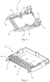
Die
Die Steckverbindermodule 4, 4' sind im Wesentlichen quaderförmig ausgestaltet. Die Steckverbindermodule 4, 4' weisen eine Steckseite S und eine Anschlussseite A auf. Mit der Steckseite S werden die Kontaktelemente 7, 7' der Steckverbindermodule 4, 4' in Steckkontakt mit Kontaktelementen eines Gegensteckverbinders (nicht zu sehen) gebracht. Auf der Anschlussseite A werden die Kontaktelemente 7, 7' jeweils mit einem Leiter eines angeschlossenen Kabels (nicht gezeigt) verbunden. Die Steckverbindermodule 5 weisen auf zwei gegenüberliegenden Seiten jeweils zwei Nuten 5, 6 auf.The
In
In
Der Leiterkartensteckverbinder 1 weist an seinen Schmalseiten jeweils einen Fixierarm 10 auf. Die Fixierarme 10 erstrecken sich steckseitig über das Steckverbindergehäuse hinaus und weisen dort endseitig Fixierhaken 13, zur reversiblen Befestigung an einem Gegensteckverbinder (nicht gezeigt) auf. Die Fixierarme 10 sind etwa mittig am zweiten Gehäuseteil 3 angeformt und über die Anformung federnd am Steckverbindergehäuse angebracht bzw. gelagert. Anschlussseitig weisen die Fixierarme 10 jeweils eine Druckplatte 11 auf. Die Druckplatte 11 ist gegen eine Anschlagfläche 12 pressbar. Dadurch weiten sich die Fixierarme 10 steckseitig auf und die Fixierhaken bewegen sich aus den Wirkbereich des Gegensteckverbinders (nicht gezeigt), so dass die Steckverbindung zwischen Leiterkartensteckverbinder 1 und Gegensteckverbinder gelöst werden kann.The printed
Steckseitig weist der Leiterkartensteckverbinder 1 in Steckrichtung weisende Führungsstege 14 auf. Dadurch wird eine passgenaue Ausrichtung des Leiterkartensteckverbinders 1 zum Gegensteckverbinder, während des Steckvorgangs, gewährleistet.On the plug-in side, the printed
Der Leiterkartensteckverbinder 1 kann, wie folgt, mit unterschiedlichen und/oder gleichartigen Steckverbindermodulen 4, 4' bestückt werden: Zunächst werden die Steckverbindermodule 4, 4' nacheinander und nebeneinander auf der Auflagenfläche 8 des ersten Gehäuseteils 2 aufgereiht. Dabei wird die hintere Nut 5 zunächst auf den segmentierten Steg 9 schräg aufgesetzt und anschließend das jeweilige Steckverbindermodul 4, 4' auf die Auflagefläche 8 gedrückt. Dieser Vorgang wird wiederholt bis sich die benötigte Anzahl an Steckverbindermodulen 4, 4' im ersten Gehäuseteil 2 befindet.The
Anschließend wird der durchlaufende Steg 9' des zweiten Gehäuseteils 3 in die vordere Nut 6 der aneinandergereihten Steckverbindermodule 4, 4' geführt. Dann wird das zweite Gehäuseteil 3 auf das erste Gehäuseteil gepresst. Die beiden Gehäuseteile 2, 3 können über Schraub- und Gewindeöffnungen 15, 16 miteinander fixiert werden, wodurch gleichzeitig auch die Steckverbindermodule 4, 4' im Leiterkartensteckverbinder 1 fixiert werden.The continuous web 9' of the second housing part 3 is then guided into the front groove 6 of the
Auch wenn in den Figuren verschiedene Aspekte oder Merkmale der Erfindung jeweils in Kombination gezeigt sind, ist für den Fachmann - soweit nicht anders angegeben - ersichtlich, dass die dargestellten und diskutierten Kombinationen nicht die einzig möglichen sind. Insbesondere können einander entsprechende Einheiten oder Merkmalskomplexe aus unterschiedlichen Ausführungsbeispielen miteinander ausgetauscht werden.Even if different aspects or features of the invention are shown in combination in the figures, it is clear to the person skilled in the art - unless otherwise stated - that the combinations shown and discussed are not the only possible ones. In particular, corresponding units or feature complexes from different embodiments can be exchanged with one another.
- 11
- LeiterkartensteckverbinderPCB connectors
- 22
- Erstes GehäuseteilFirst housing part
- 33
- Zweites GehäuseteilSecond housing part
- 44
- SteckverbindermodulConnector module
- 55
- Hintere NutRear groove
- 66
- Vordere NutFront groove
- 77
- KontaktelementContact element
- 88th
- AuflageflächeSupport surface
- 99
- Stegweb
- 1010
- FixierarmeFixing arms
- 1111
- Druckplatteprinting plate
- 1212
- AnschlagflächeStop surface
- 1313
- FixierhakenFixing hook
- 1414
- FührungsstegeGuide rails
- 1515
- SchrauböffnungScrew opening
- 1616
- GewindeöffnungThreaded opening
- SS
- SteckseitePlug-in side
- AA
- AnschlussseiteConnection side
Claims (7)
- Modular printed-circuit-board plug connector (1), wherein the printed-circuit-board plug connector (1) has at least one first housing part (2) and one second housing part (3) which are able to be joined together to form a plug-connector housing; and wherein the printed-circuit-board plug connector (1) has at least two different plug-connector modules (4, 4') which are held in a pluggable manner in the plug-connector housing by the joined-together housing parts (2, 3),
characterized in thatthe plug-connector modules (4, 4') are of substantially cuboidal design and have on two oppositely situated surfaces in each case two parallel grooves, a rear groove (5) and a front groove (6),in that the plug-connector modules (4, 4') are able to be placed one next to the other on a plugging-side bearing surface (8) of the first housing part (2, 2'), andin that, on the edge of the bearing surface (8), there is arranged a segmented web (9) which engages into the rear groove (5) of the plug-connector module (4, 4'). - Modular printed-circuit-board plug connector according to Claim 1,
characterized in that
the printed-circuit-board plug connector (1) has on its narrow sides fixing arms (10) by way of which the printed-circuit-board plug connector (1) is able to be fixed reversibly to a counterpart plug connector which is arranged on a printed circuit board. - Modular printed-circuit-board plug connector according to the preceding claim,
characterized in that
the fixing arms (10) are integrally formed on the second housing part (3). - Modular printed-circuit-board plug connector according to either of the two preceding claims,
characterized in that
the fixing arms (10) are integrally formed on the plug-connector housing so as to be movable orthogonally to the plugging direction. - Modular printed-circuit-board plug connector according to one of the three preceding claims,
characterized in that
the fixing arms (10) extend along the narrow sides of the printed-circuit-board plug connector (1). - Modular printed-circuit-board plug connector according to one of the four preceding claims,
characterized in that
the fixing arms (10) each have a pressing plate (11) on the connection side, wherein the pressing plates (11) are able to be pressed towards one another, whereby the printed-circuit-board plug connector (1) is unlocked from a counterpart plug connector and is able to be separated from the latter. - Modular printed-circuit-board plug connector according to one of the preceding claims,
characterized in that
the housing parts (2, 3) each consist of plastic.
Applications Claiming Priority (2)
| Application Number | Priority Date | Filing Date | Title |
|---|---|---|---|
| DE102019115177.5A DE102019115177A1 (en) | 2019-06-05 | 2019-06-05 | Modular PCB connector |
| PCT/DE2020/100449 WO2020244706A1 (en) | 2019-06-05 | 2020-05-27 | Modular circuit board plug connector |
Publications (2)
| Publication Number | Publication Date |
|---|---|
| EP3981046A1 EP3981046A1 (en) | 2022-04-13 |
| EP3981046B1 true EP3981046B1 (en) | 2024-07-03 |
Family
ID=71094057
Family Applications (1)
| Application Number | Title | Priority Date | Filing Date |
|---|---|---|---|
| EP20732722.2A Active EP3981046B1 (en) | 2019-06-05 | 2020-05-27 | Modular circuit board plug connector |
Country Status (7)
| Country | Link |
|---|---|
| US (1) | US12126111B2 (en) |
| EP (1) | EP3981046B1 (en) |
| KR (1) | KR102723220B1 (en) |
| CN (1) | CN113906636A (en) |
| DE (1) | DE102019115177A1 (en) |
| PL (1) | PL3981046T3 (en) |
| WO (1) | WO2020244706A1 (en) |
Families Citing this family (3)
| Publication number | Priority date | Publication date | Assignee | Title |
|---|---|---|---|---|
| DE102021130351A1 (en) * | 2021-11-19 | 2023-05-25 | Weidmüller Interface GmbH & Co. KG | Modular connector for contacting a mating connector, in particular a printed circuit board connector |
| TWM631360U (en) * | 2022-01-25 | 2022-09-01 | 貝爾威勒電子股份有限公司 | Plug connector with protective structure |
| DE102024101483A1 (en) | 2024-01-18 | 2025-07-24 | Harting Electric Stiftung & Co. Kg | Modular PCB connector |
Family Cites Families (16)
| Publication number | Priority date | Publication date | Assignee | Title |
|---|---|---|---|---|
| GB8425406D0 (en) * | 1984-10-08 | 1984-11-14 | Electronic Components Ltd | Electrical contact housing |
| US5108313A (en) * | 1989-10-05 | 1992-04-28 | E. I. Du Pont De Nemours And Company | Modular connector |
| DE29602740U1 (en) * | 1996-02-21 | 1996-04-11 | Phoenix Contact GmbH & Co, 32825 Blomberg | Electrical connector |
| DE29603740U1 (en) | 1996-02-29 | 1996-07-11 | F2 International Ges.M.B.H., Kirchdorf | Floats, especially windsurf boards |
| US5924898A (en) * | 1997-05-29 | 1999-07-20 | Raychem Corporation | Modular connector |
| US6231392B1 (en) * | 1997-10-01 | 2001-05-15 | Berg Technology, Inc. | Cable interconnection |
| FR2781092B1 (en) * | 1998-07-10 | 2000-10-06 | Framatome Connectors France | MODULAR CONNECTOR WITH FLOATING INSERTS |
| TW405762U (en) | 1998-11-11 | 2000-09-11 | Molex Inc | Connector |
| DE29904381U1 (en) | 1999-03-10 | 2000-08-10 | Robert Bosch Gmbh, 70469 Stuttgart | Electrical plug device with a fixing device |
| DE20205787U1 (en) | 2002-04-13 | 2002-07-25 | HARTING Electric GmbH & Co. KG, 32339 Espelkamp | Modular connector |
| DE102004017605B3 (en) | 2004-04-07 | 2005-10-20 | Adc Gmbh | Connectors for printed circuit boards and distributor connection module |
| US8210876B2 (en) | 2006-05-23 | 2012-07-03 | Fci | Connector, connector assembling system and method of assembling a connector |
| US7762846B1 (en) * | 2009-09-15 | 2010-07-27 | Tyco Electronics Corporation | Connector assembly having a back shell |
| US8961217B2 (en) * | 2013-03-12 | 2015-02-24 | Carlisle Interconnect Technologies, Inc. | Electrical connector assembly with integrated latching system, strain relief, and EMI shielding |
| WO2018206048A1 (en) * | 2017-05-12 | 2018-11-15 | Harting Electric Gmbh & Co. Kg | Plug connector module |
| DE102017119287B4 (en) * | 2017-08-23 | 2019-08-08 | HARTING Electronics GmbH | Modular connector for printed circuit boards |
-
2019
- 2019-06-05 DE DE102019115177.5A patent/DE102019115177A1/en active Pending
-
2020
- 2020-05-27 PL PL20732722.2T patent/PL3981046T3/en unknown
- 2020-05-27 US US17/615,070 patent/US12126111B2/en active Active
- 2020-05-27 CN CN202080040746.9A patent/CN113906636A/en active Pending
- 2020-05-27 KR KR1020227000039A patent/KR102723220B1/en active Active
- 2020-05-27 EP EP20732722.2A patent/EP3981046B1/en active Active
- 2020-05-27 WO PCT/DE2020/100449 patent/WO2020244706A1/en not_active Ceased
Also Published As
| Publication number | Publication date |
|---|---|
| CN113906636A (en) | 2022-01-07 |
| EP3981046A1 (en) | 2022-04-13 |
| US20220224042A1 (en) | 2022-07-14 |
| KR20220008377A (en) | 2022-01-20 |
| US12126111B2 (en) | 2024-10-22 |
| DE102019115177A1 (en) | 2020-12-10 |
| PL3981046T3 (en) | 2024-11-18 |
| WO2020244706A1 (en) | 2020-12-10 |
| KR102723220B1 (en) | 2024-10-30 |
Similar Documents
| Publication | Publication Date | Title |
|---|---|---|
| DE102006016882B4 (en) | Connectors | |
| DE69309438T2 (en) | SYSTEM AND CONNECTOR FOR THE ELECTRICAL CONNECTION OF CIRCUIT BOARDS | |
| DE69525623T2 (en) | Electrical connector with improved locking system | |
| DE102017119287B4 (en) | Modular connector for printed circuit boards | |
| DE69018454T2 (en) | CODING SYSTEM FOR CONNECTORS. | |
| EP3474646B1 (en) | Support rail housing, electronic module with a support rail housing and system, in particular control system, with a plurality of electronic modules | |
| DE3843664C2 (en) | ||
| EP3930107B1 (en) | Modular mounting frame for connector | |
| EP3981046B1 (en) | Modular circuit board plug connector | |
| EP2018684B1 (en) | Module with connectors for actuators and/or sensors | |
| EP3766136A1 (en) | Printed circuit board connector | |
| DE3318137C2 (en) | Multipole electrical connector | |
| DE19627481C2 (en) | Electrical switch and fuse device | |
| WO2020207529A1 (en) | Arrangement of modular plug connectors for a printed circuit board | |
| DE68919628T2 (en) | Electrical connector. | |
| DE4433735A1 (en) | Swivel connector for planar electronic devices | |
| DE10005310C2 (en) | Connectors | |
| DE3784023T2 (en) | ELECTRICAL CONNECTOR, WHICH INCLUDES A COMBINATION OF INDIVIDUAL ADAPTERS AND CONNECTOR ELEMENTS AS A CONTACT LINK. | |
| DE9415087U1 (en) | Pluggable electrical connection device | |
| DE202016101373U1 (en) | Electrical contact element for a bus element of a mounting rail bus system | |
| DE9014856U1 (en) | Insulating body for electrical contacts | |
| EP0457254A2 (en) | Holding device for electrical components, in particular for telecommunication | |
| EP4385100B1 (en) | Device and method for connecting two printed circuit board plug connectors via a coupling element | |
| DE69725269T2 (en) | Electrical connector with pin holder | |
| DE4026124A1 (en) | CONNECTING SOCKET FOR ELECTRICAL CABLES |
Legal Events
| Date | Code | Title | Description |
|---|---|---|---|
| STAA | Information on the status of an ep patent application or granted ep patent |
Free format text: STATUS: UNKNOWN |
|
| STAA | Information on the status of an ep patent application or granted ep patent |
Free format text: STATUS: THE INTERNATIONAL PUBLICATION HAS BEEN MADE |
|
| PUAI | Public reference made under article 153(3) epc to a published international application that has entered the european phase |
Free format text: ORIGINAL CODE: 0009012 |
|
| STAA | Information on the status of an ep patent application or granted ep patent |
Free format text: STATUS: REQUEST FOR EXAMINATION WAS MADE |
|
| 17P | Request for examination filed |
Effective date: 20211222 |
|
| AK | Designated contracting states |
Kind code of ref document: A1 Designated state(s): AL AT BE BG CH CY CZ DE DK EE ES FI FR GB GR HR HU IE IS IT LI LT LU LV MC MK MT NL NO PL PT RO RS SE SI SK SM TR |
|
| DAV | Request for validation of the european patent (deleted) | ||
| DAX | Request for extension of the european patent (deleted) | ||
| P01 | Opt-out of the competence of the unified patent court (upc) registered |
Effective date: 20230603 |
|
| GRAP | Despatch of communication of intention to grant a patent |
Free format text: ORIGINAL CODE: EPIDOSNIGR1 |
|
| STAA | Information on the status of an ep patent application or granted ep patent |
Free format text: STATUS: GRANT OF PATENT IS INTENDED |
|
| INTG | Intention to grant announced |
Effective date: 20240226 |
|
| GRAS | Grant fee paid |
Free format text: ORIGINAL CODE: EPIDOSNIGR3 |
|
| GRAA | (expected) grant |
Free format text: ORIGINAL CODE: 0009210 |
|
| STAA | Information on the status of an ep patent application or granted ep patent |
Free format text: STATUS: THE PATENT HAS BEEN GRANTED |
|
| RAP3 | Party data changed (applicant data changed or rights of an application transferred) |
Owner name: HARTING ELECTRIC STIFTUNG & CO. KG |
|
| AK | Designated contracting states |
Kind code of ref document: B1 Designated state(s): AL AT BE BG CH CY CZ DE DK EE ES FI FR GB GR HR HU IE IS IT LI LT LU LV MC MK MT NL NO PL PT RO RS SE SI SK SM TR |
|
| REG | Reference to a national code |
Ref country code: CH Ref legal event code: EP |
|
| REG | Reference to a national code |
Ref country code: DE Ref legal event code: R096 Ref document number: 502020008470 Country of ref document: DE |
|
| REG | Reference to a national code |
Ref country code: LT Ref legal event code: MG9D |
|
| REG | Reference to a national code |
Ref country code: NL Ref legal event code: MP Effective date: 20240703 |
|
| PG25 | Lapsed in a contracting state [announced via postgrant information from national office to epo] |
Ref country code: PT Free format text: LAPSE BECAUSE OF FAILURE TO SUBMIT A TRANSLATION OF THE DESCRIPTION OR TO PAY THE FEE WITHIN THE PRESCRIBED TIME-LIMIT Effective date: 20241104 |
|
| PG25 | Lapsed in a contracting state [announced via postgrant information from national office to epo] |
Ref country code: NL Free format text: LAPSE BECAUSE OF FAILURE TO SUBMIT A TRANSLATION OF THE DESCRIPTION OR TO PAY THE FEE WITHIN THE PRESCRIBED TIME-LIMIT Effective date: 20240703 |
|
| PG25 | Lapsed in a contracting state [announced via postgrant information from national office to epo] |
Ref country code: PT Free format text: LAPSE BECAUSE OF FAILURE TO SUBMIT A TRANSLATION OF THE DESCRIPTION OR TO PAY THE FEE WITHIN THE PRESCRIBED TIME-LIMIT Effective date: 20241104 Ref country code: NL Free format text: LAPSE BECAUSE OF FAILURE TO SUBMIT A TRANSLATION OF THE DESCRIPTION OR TO PAY THE FEE WITHIN THE PRESCRIBED TIME-LIMIT Effective date: 20240703 |
|
| PG25 | Lapsed in a contracting state [announced via postgrant information from national office to epo] |
Ref country code: NO Free format text: LAPSE BECAUSE OF FAILURE TO SUBMIT A TRANSLATION OF THE DESCRIPTION OR TO PAY THE FEE WITHIN THE PRESCRIBED TIME-LIMIT Effective date: 20241003 |
|
| PG25 | Lapsed in a contracting state [announced via postgrant information from national office to epo] |
Ref country code: GR Free format text: LAPSE BECAUSE OF FAILURE TO SUBMIT A TRANSLATION OF THE DESCRIPTION OR TO PAY THE FEE WITHIN THE PRESCRIBED TIME-LIMIT Effective date: 20241004 Ref country code: FI Free format text: LAPSE BECAUSE OF FAILURE TO SUBMIT A TRANSLATION OF THE DESCRIPTION OR TO PAY THE FEE WITHIN THE PRESCRIBED TIME-LIMIT Effective date: 20240703 |
|
| PG25 | Lapsed in a contracting state [announced via postgrant information from national office to epo] |
Ref country code: BG Free format text: LAPSE BECAUSE OF FAILURE TO SUBMIT A TRANSLATION OF THE DESCRIPTION OR TO PAY THE FEE WITHIN THE PRESCRIBED TIME-LIMIT Effective date: 20240703 |
|
| PG25 | Lapsed in a contracting state [announced via postgrant information from national office to epo] |
Ref country code: LV Free format text: LAPSE BECAUSE OF FAILURE TO SUBMIT A TRANSLATION OF THE DESCRIPTION OR TO PAY THE FEE WITHIN THE PRESCRIBED TIME-LIMIT Effective date: 20240703 |
|
| PG25 | Lapsed in a contracting state [announced via postgrant information from national office to epo] |
Ref country code: IS Free format text: LAPSE BECAUSE OF FAILURE TO SUBMIT A TRANSLATION OF THE DESCRIPTION OR TO PAY THE FEE WITHIN THE PRESCRIBED TIME-LIMIT Effective date: 20241103 |
|
| PG25 | Lapsed in a contracting state [announced via postgrant information from national office to epo] |
Ref country code: CZ Free format text: LAPSE BECAUSE OF FAILURE TO SUBMIT A TRANSLATION OF THE DESCRIPTION OR TO PAY THE FEE WITHIN THE PRESCRIBED TIME-LIMIT Effective date: 20240703 Ref country code: HR Free format text: LAPSE BECAUSE OF FAILURE TO SUBMIT A TRANSLATION OF THE DESCRIPTION OR TO PAY THE FEE WITHIN THE PRESCRIBED TIME-LIMIT Effective date: 20240703 |
|
| PG25 | Lapsed in a contracting state [announced via postgrant information from national office to epo] |
Ref country code: ES Free format text: LAPSE BECAUSE OF FAILURE TO SUBMIT A TRANSLATION OF THE DESCRIPTION OR TO PAY THE FEE WITHIN THE PRESCRIBED TIME-LIMIT Effective date: 20240703 Ref country code: RS Free format text: LAPSE BECAUSE OF FAILURE TO SUBMIT A TRANSLATION OF THE DESCRIPTION OR TO PAY THE FEE WITHIN THE PRESCRIBED TIME-LIMIT Effective date: 20241003 |
|
| PG25 | Lapsed in a contracting state [announced via postgrant information from national office to epo] |
Ref country code: RS Free format text: LAPSE BECAUSE OF FAILURE TO SUBMIT A TRANSLATION OF THE DESCRIPTION OR TO PAY THE FEE WITHIN THE PRESCRIBED TIME-LIMIT Effective date: 20241003 Ref country code: NO Free format text: LAPSE BECAUSE OF FAILURE TO SUBMIT A TRANSLATION OF THE DESCRIPTION OR TO PAY THE FEE WITHIN THE PRESCRIBED TIME-LIMIT Effective date: 20241003 Ref country code: LV Free format text: LAPSE BECAUSE OF FAILURE TO SUBMIT A TRANSLATION OF THE DESCRIPTION OR TO PAY THE FEE WITHIN THE PRESCRIBED TIME-LIMIT Effective date: 20240703 Ref country code: IS Free format text: LAPSE BECAUSE OF FAILURE TO SUBMIT A TRANSLATION OF THE DESCRIPTION OR TO PAY THE FEE WITHIN THE PRESCRIBED TIME-LIMIT Effective date: 20241103 Ref country code: HR Free format text: LAPSE BECAUSE OF FAILURE TO SUBMIT A TRANSLATION OF THE DESCRIPTION OR TO PAY THE FEE WITHIN THE PRESCRIBED TIME-LIMIT Effective date: 20240703 Ref country code: GR Free format text: LAPSE BECAUSE OF FAILURE TO SUBMIT A TRANSLATION OF THE DESCRIPTION OR TO PAY THE FEE WITHIN THE PRESCRIBED TIME-LIMIT Effective date: 20241004 Ref country code: FI Free format text: LAPSE BECAUSE OF FAILURE TO SUBMIT A TRANSLATION OF THE DESCRIPTION OR TO PAY THE FEE WITHIN THE PRESCRIBED TIME-LIMIT Effective date: 20240703 Ref country code: ES Free format text: LAPSE BECAUSE OF FAILURE TO SUBMIT A TRANSLATION OF THE DESCRIPTION OR TO PAY THE FEE WITHIN THE PRESCRIBED TIME-LIMIT Effective date: 20240703 Ref country code: CZ Free format text: LAPSE BECAUSE OF FAILURE TO SUBMIT A TRANSLATION OF THE DESCRIPTION OR TO PAY THE FEE WITHIN THE PRESCRIBED TIME-LIMIT Effective date: 20240703 Ref country code: BG Free format text: LAPSE BECAUSE OF FAILURE TO SUBMIT A TRANSLATION OF THE DESCRIPTION OR TO PAY THE FEE WITHIN THE PRESCRIBED TIME-LIMIT Effective date: 20240703 |
|
| REG | Reference to a national code |
Ref country code: DE Ref legal event code: R097 Ref document number: 502020008470 Country of ref document: DE |
|
| PG25 | Lapsed in a contracting state [announced via postgrant information from national office to epo] |
Ref country code: RO Free format text: LAPSE BECAUSE OF FAILURE TO SUBMIT A TRANSLATION OF THE DESCRIPTION OR TO PAY THE FEE WITHIN THE PRESCRIBED TIME-LIMIT Effective date: 20240703 Ref country code: SM Free format text: LAPSE BECAUSE OF FAILURE TO SUBMIT A TRANSLATION OF THE DESCRIPTION OR TO PAY THE FEE WITHIN THE PRESCRIBED TIME-LIMIT Effective date: 20240703 Ref country code: DK Free format text: LAPSE BECAUSE OF FAILURE TO SUBMIT A TRANSLATION OF THE DESCRIPTION OR TO PAY THE FEE WITHIN THE PRESCRIBED TIME-LIMIT Effective date: 20240703 |
|
| PG25 | Lapsed in a contracting state [announced via postgrant information from national office to epo] |
Ref country code: EE Free format text: LAPSE BECAUSE OF FAILURE TO SUBMIT A TRANSLATION OF THE DESCRIPTION OR TO PAY THE FEE WITHIN THE PRESCRIBED TIME-LIMIT Effective date: 20240703 |
|
| PG25 | Lapsed in a contracting state [announced via postgrant information from national office to epo] |
Ref country code: SK Free format text: LAPSE BECAUSE OF FAILURE TO SUBMIT A TRANSLATION OF THE DESCRIPTION OR TO PAY THE FEE WITHIN THE PRESCRIBED TIME-LIMIT Effective date: 20240703 |
|
| PLBE | No opposition filed within time limit |
Free format text: ORIGINAL CODE: 0009261 |
|
| STAA | Information on the status of an ep patent application or granted ep patent |
Free format text: STATUS: NO OPPOSITION FILED WITHIN TIME LIMIT |
|
| 26N | No opposition filed |
Effective date: 20250404 |
|
| PGFP | Annual fee paid to national office [announced via postgrant information from national office to epo] |
Ref country code: PL Payment date: 20250526 Year of fee payment: 6 Ref country code: DE Payment date: 20250528 Year of fee payment: 6 |
|
| PGFP | Annual fee paid to national office [announced via postgrant information from national office to epo] |
Ref country code: GB Payment date: 20250520 Year of fee payment: 6 |
|
| PGFP | Annual fee paid to national office [announced via postgrant information from national office to epo] |
Ref country code: IT Payment date: 20250522 Year of fee payment: 6 |
|
| PGFP | Annual fee paid to national office [announced via postgrant information from national office to epo] |
Ref country code: FR Payment date: 20250526 Year of fee payment: 6 |
|
| PG25 | Lapsed in a contracting state [announced via postgrant information from national office to epo] |
Ref country code: SE Free format text: LAPSE BECAUSE OF FAILURE TO SUBMIT A TRANSLATION OF THE DESCRIPTION OR TO PAY THE FEE WITHIN THE PRESCRIBED TIME-LIMIT Effective date: 20240703 |
|
| REG | Reference to a national code |
Ref country code: CH Ref legal event code: H13 Free format text: ST27 STATUS EVENT CODE: U-0-0-H10-H13 (AS PROVIDED BY THE NATIONAL OFFICE) Effective date: 20251223 |
|
| PG25 | Lapsed in a contracting state [announced via postgrant information from national office to epo] |
Ref country code: LU Free format text: LAPSE BECAUSE OF NON-PAYMENT OF DUE FEES Effective date: 20250527 |
|
| PG25 | Lapsed in a contracting state [announced via postgrant information from national office to epo] |
Ref country code: CH Free format text: LAPSE BECAUSE OF NON-PAYMENT OF DUE FEES Effective date: 20250531 |
|
| REG | Reference to a national code |
Ref country code: BE Ref legal event code: MM Effective date: 20250531 |
|
| PG25 | Lapsed in a contracting state [announced via postgrant information from national office to epo] |
Ref country code: MC Free format text: LAPSE BECAUSE OF FAILURE TO SUBMIT A TRANSLATION OF THE DESCRIPTION OR TO PAY THE FEE WITHIN THE PRESCRIBED TIME-LIMIT Effective date: 20240703 |
|
| PG25 | Lapsed in a contracting state [announced via postgrant information from national office to epo] |
Ref country code: IE Free format text: LAPSE BECAUSE OF NON-PAYMENT OF DUE FEES Effective date: 20250527 |
|
| PG25 | Lapsed in a contracting state [announced via postgrant information from national office to epo] |
Ref country code: BE Free format text: LAPSE BECAUSE OF NON-PAYMENT OF DUE FEES Effective date: 20250531 |