EP3712693B1 - Dispositif de commande de lumière, dispositif d'affichage d'image et dispositif d'affichage - Google Patents
Dispositif de commande de lumière, dispositif d'affichage d'image et dispositif d'affichage Download PDFInfo
- Publication number
- EP3712693B1 EP3712693B1 EP18877556.3A EP18877556A EP3712693B1 EP 3712693 B1 EP3712693 B1 EP 3712693B1 EP 18877556 A EP18877556 A EP 18877556A EP 3712693 B1 EP3712693 B1 EP 3712693B1
- Authority
- EP
- European Patent Office
- Prior art keywords
- light
- dimming
- display device
- substrate
- coloring layer
- Prior art date
- Legal status (The legal status is an assumption and is not a legal conclusion. Google has not performed a legal analysis and makes no representation as to the accuracy of the status listed.)
- Active
Links
Images

















Classifications
-
- G—PHYSICS
- G02—OPTICS
- G02F—OPTICAL DEVICES OR ARRANGEMENTS FOR THE CONTROL OF LIGHT BY MODIFICATION OF THE OPTICAL PROPERTIES OF THE MEDIA OF THE ELEMENTS INVOLVED THEREIN; NON-LINEAR OPTICS; FREQUENCY-CHANGING OF LIGHT; OPTICAL LOGIC ELEMENTS; OPTICAL ANALOGUE/DIGITAL CONVERTERS
- G02F1/00—Devices or arrangements for the control of the intensity, colour, phase, polarisation or direction of light arriving from an independent light source, e.g. switching, gating or modulating; Non-linear optics
- G02F1/01—Devices or arrangements for the control of the intensity, colour, phase, polarisation or direction of light arriving from an independent light source, e.g. switching, gating or modulating; Non-linear optics for the control of the intensity, phase, polarisation or colour
- G02F1/15—Devices or arrangements for the control of the intensity, colour, phase, polarisation or direction of light arriving from an independent light source, e.g. switching, gating or modulating; Non-linear optics for the control of the intensity, phase, polarisation or colour based on an electrochromic effect
- G02F1/1514—Devices or arrangements for the control of the intensity, colour, phase, polarisation or direction of light arriving from an independent light source, e.g. switching, gating or modulating; Non-linear optics for the control of the intensity, phase, polarisation or colour based on an electrochromic effect characterised by the electrochromic material, e.g. by the electrodeposited material
- G02F1/1523—Devices or arrangements for the control of the intensity, colour, phase, polarisation or direction of light arriving from an independent light source, e.g. switching, gating or modulating; Non-linear optics for the control of the intensity, phase, polarisation or colour based on an electrochromic effect characterised by the electrochromic material, e.g. by the electrodeposited material comprising inorganic material
- G02F1/1524—Transition metal compounds
-
- G—PHYSICS
- G02—OPTICS
- G02F—OPTICAL DEVICES OR ARRANGEMENTS FOR THE CONTROL OF LIGHT BY MODIFICATION OF THE OPTICAL PROPERTIES OF THE MEDIA OF THE ELEMENTS INVOLVED THEREIN; NON-LINEAR OPTICS; FREQUENCY-CHANGING OF LIGHT; OPTICAL LOGIC ELEMENTS; OPTICAL ANALOGUE/DIGITAL CONVERTERS
- G02F1/00—Devices or arrangements for the control of the intensity, colour, phase, polarisation or direction of light arriving from an independent light source, e.g. switching, gating or modulating; Non-linear optics
- G02F1/01—Devices or arrangements for the control of the intensity, colour, phase, polarisation or direction of light arriving from an independent light source, e.g. switching, gating or modulating; Non-linear optics for the control of the intensity, phase, polarisation or colour
- G02F1/15—Devices or arrangements for the control of the intensity, colour, phase, polarisation or direction of light arriving from an independent light source, e.g. switching, gating or modulating; Non-linear optics for the control of the intensity, phase, polarisation or colour based on an electrochromic effect
-
- G—PHYSICS
- G06—COMPUTING OR CALCULATING; COUNTING
- G06F—ELECTRIC DIGITAL DATA PROCESSING
- G06F3/00—Input arrangements for transferring data to be processed into a form capable of being handled by the computer; Output arrangements for transferring data from processing unit to output unit, e.g. interface arrangements
- G06F3/14—Digital output to display device ; Cooperation and interconnection of the display device with other functional units
- G06F3/147—Digital output to display device ; Cooperation and interconnection of the display device with other functional units using display panels
-
- G—PHYSICS
- G02—OPTICS
- G02B—OPTICAL ELEMENTS, SYSTEMS OR APPARATUS
- G02B27/00—Optical systems or apparatus not provided for by any of the groups G02B1/00 - G02B26/00, G02B30/00
- G02B27/01—Head-up displays
- G02B27/017—Head mounted
- G02B27/0172—Head mounted characterised by optical features
-
- G—PHYSICS
- G02—OPTICS
- G02B—OPTICAL ELEMENTS, SYSTEMS OR APPARATUS
- G02B27/00—Optical systems or apparatus not provided for by any of the groups G02B1/00 - G02B26/00, G02B30/00
- G02B27/02—Viewing or reading apparatus
-
- G—PHYSICS
- G02—OPTICS
- G02F—OPTICAL DEVICES OR ARRANGEMENTS FOR THE CONTROL OF LIGHT BY MODIFICATION OF THE OPTICAL PROPERTIES OF THE MEDIA OF THE ELEMENTS INVOLVED THEREIN; NON-LINEAR OPTICS; FREQUENCY-CHANGING OF LIGHT; OPTICAL LOGIC ELEMENTS; OPTICAL ANALOGUE/DIGITAL CONVERTERS
- G02F1/00—Devices or arrangements for the control of the intensity, colour, phase, polarisation or direction of light arriving from an independent light source, e.g. switching, gating or modulating; Non-linear optics
- G02F1/01—Devices or arrangements for the control of the intensity, colour, phase, polarisation or direction of light arriving from an independent light source, e.g. switching, gating or modulating; Non-linear optics for the control of the intensity, phase, polarisation or colour
- G02F1/15—Devices or arrangements for the control of the intensity, colour, phase, polarisation or direction of light arriving from an independent light source, e.g. switching, gating or modulating; Non-linear optics for the control of the intensity, phase, polarisation or colour based on an electrochromic effect
- G02F1/1514—Devices or arrangements for the control of the intensity, colour, phase, polarisation or direction of light arriving from an independent light source, e.g. switching, gating or modulating; Non-linear optics for the control of the intensity, phase, polarisation or colour based on an electrochromic effect characterised by the electrochromic material, e.g. by the electrodeposited material
- G02F1/1523—Devices or arrangements for the control of the intensity, colour, phase, polarisation or direction of light arriving from an independent light source, e.g. switching, gating or modulating; Non-linear optics for the control of the intensity, phase, polarisation or colour based on an electrochromic effect characterised by the electrochromic material, e.g. by the electrodeposited material comprising inorganic material
- G02F1/1524—Transition metal compounds
- G02F1/15245—Transition metal compounds based on iridium oxide or hydroxide
-
- G—PHYSICS
- G09—EDUCATION; CRYPTOGRAPHY; DISPLAY; ADVERTISING; SEALS
- G09F—DISPLAYING; ADVERTISING; SIGNS; LABELS OR NAME-PLATES; SEALS
- G09F9/00—Indicating arrangements for variable information in which the information is built-up on a support by selection or combination of individual elements
-
- G—PHYSICS
- G09—EDUCATION; CRYPTOGRAPHY; DISPLAY; ADVERTISING; SEALS
- G09G—ARRANGEMENTS OR CIRCUITS FOR CONTROL OF INDICATING DEVICES USING STATIC MEANS TO PRESENT VARIABLE INFORMATION
- G09G3/00—Control arrangements or circuits, of interest only in connection with visual indicators other than cathode-ray tubes
- G09G3/20—Control arrangements or circuits, of interest only in connection with visual indicators other than cathode-ray tubes for presentation of an assembly of a number of characters, e.g. a page, by composing the assembly by combination of individual elements arranged in a matrix no fixed position being assigned to or needed to be assigned to the individual characters or partial characters
-
- G—PHYSICS
- G09—EDUCATION; CRYPTOGRAPHY; DISPLAY; ADVERTISING; SEALS
- G09G—ARRANGEMENTS OR CIRCUITS FOR CONTROL OF INDICATING DEVICES USING STATIC MEANS TO PRESENT VARIABLE INFORMATION
- G09G3/00—Control arrangements or circuits, of interest only in connection with visual indicators other than cathode-ray tubes
- G09G3/20—Control arrangements or circuits, of interest only in connection with visual indicators other than cathode-ray tubes for presentation of an assembly of a number of characters, e.g. a page, by composing the assembly by combination of individual elements arranged in a matrix no fixed position being assigned to or needed to be assigned to the individual characters or partial characters
- G09G3/34—Control arrangements or circuits, of interest only in connection with visual indicators other than cathode-ray tubes for presentation of an assembly of a number of characters, e.g. a page, by composing the assembly by combination of individual elements arranged in a matrix no fixed position being assigned to or needed to be assigned to the individual characters or partial characters by control of light from an independent source
-
- G—PHYSICS
- G09—EDUCATION; CRYPTOGRAPHY; DISPLAY; ADVERTISING; SEALS
- G09G—ARRANGEMENTS OR CIRCUITS FOR CONTROL OF INDICATING DEVICES USING STATIC MEANS TO PRESENT VARIABLE INFORMATION
- G09G3/00—Control arrangements or circuits, of interest only in connection with visual indicators other than cathode-ray tubes
- G09G3/20—Control arrangements or circuits, of interest only in connection with visual indicators other than cathode-ray tubes for presentation of an assembly of a number of characters, e.g. a page, by composing the assembly by combination of individual elements arranged in a matrix no fixed position being assigned to or needed to be assigned to the individual characters or partial characters
- G09G3/34—Control arrangements or circuits, of interest only in connection with visual indicators other than cathode-ray tubes for presentation of an assembly of a number of characters, e.g. a page, by composing the assembly by combination of individual elements arranged in a matrix no fixed position being assigned to or needed to be assigned to the individual characters or partial characters by control of light from an independent source
- G09G3/38—Control arrangements or circuits, of interest only in connection with visual indicators other than cathode-ray tubes for presentation of an assembly of a number of characters, e.g. a page, by composing the assembly by combination of individual elements arranged in a matrix no fixed position being assigned to or needed to be assigned to the individual characters or partial characters by control of light from an independent source using electrochromic devices
-
- G—PHYSICS
- G09—EDUCATION; CRYPTOGRAPHY; DISPLAY; ADVERTISING; SEALS
- G09G—ARRANGEMENTS OR CIRCUITS FOR CONTROL OF INDICATING DEVICES USING STATIC MEANS TO PRESENT VARIABLE INFORMATION
- G09G5/00—Control arrangements or circuits for visual indicators common to cathode-ray tube indicators and other visual indicators
- G09G5/10—Intensity circuits
-
- G—PHYSICS
- G02—OPTICS
- G02B—OPTICAL ELEMENTS, SYSTEMS OR APPARATUS
- G02B27/00—Optical systems or apparatus not provided for by any of the groups G02B1/00 - G02B26/00, G02B30/00
- G02B27/01—Head-up displays
- G02B27/0101—Head-up displays characterised by optical features
- G02B2027/0118—Head-up displays characterised by optical features comprising devices for improving the contrast of the display / brillance control visibility
-
- G—PHYSICS
- G02—OPTICS
- G02F—OPTICAL DEVICES OR ARRANGEMENTS FOR THE CONTROL OF LIGHT BY MODIFICATION OF THE OPTICAL PROPERTIES OF THE MEDIA OF THE ELEMENTS INVOLVED THEREIN; NON-LINEAR OPTICS; FREQUENCY-CHANGING OF LIGHT; OPTICAL LOGIC ELEMENTS; OPTICAL ANALOGUE/DIGITAL CONVERTERS
- G02F1/00—Devices or arrangements for the control of the intensity, colour, phase, polarisation or direction of light arriving from an independent light source, e.g. switching, gating or modulating; Non-linear optics
- G02F1/01—Devices or arrangements for the control of the intensity, colour, phase, polarisation or direction of light arriving from an independent light source, e.g. switching, gating or modulating; Non-linear optics for the control of the intensity, phase, polarisation or colour
- G02F1/15—Devices or arrangements for the control of the intensity, colour, phase, polarisation or direction of light arriving from an independent light source, e.g. switching, gating or modulating; Non-linear optics for the control of the intensity, phase, polarisation or colour based on an electrochromic effect
- G02F1/153—Constructional details
- G02F1/155—Electrodes
-
- G—PHYSICS
- G02—OPTICS
- G02F—OPTICAL DEVICES OR ARRANGEMENTS FOR THE CONTROL OF LIGHT BY MODIFICATION OF THE OPTICAL PROPERTIES OF THE MEDIA OF THE ELEMENTS INVOLVED THEREIN; NON-LINEAR OPTICS; FREQUENCY-CHANGING OF LIGHT; OPTICAL LOGIC ELEMENTS; OPTICAL ANALOGUE/DIGITAL CONVERTERS
- G02F1/00—Devices or arrangements for the control of the intensity, colour, phase, polarisation or direction of light arriving from an independent light source, e.g. switching, gating or modulating; Non-linear optics
- G02F1/01—Devices or arrangements for the control of the intensity, colour, phase, polarisation or direction of light arriving from an independent light source, e.g. switching, gating or modulating; Non-linear optics for the control of the intensity, phase, polarisation or colour
- G02F1/15—Devices or arrangements for the control of the intensity, colour, phase, polarisation or direction of light arriving from an independent light source, e.g. switching, gating or modulating; Non-linear optics for the control of the intensity, phase, polarisation or colour based on an electrochromic effect
- G02F1/153—Constructional details
- G02F1/157—Structural association of cells with optical devices, e.g. reflectors or illuminating devices
-
- G—PHYSICS
- G02—OPTICS
- G02F—OPTICAL DEVICES OR ARRANGEMENTS FOR THE CONTROL OF LIGHT BY MODIFICATION OF THE OPTICAL PROPERTIES OF THE MEDIA OF THE ELEMENTS INVOLVED THEREIN; NON-LINEAR OPTICS; FREQUENCY-CHANGING OF LIGHT; OPTICAL LOGIC ELEMENTS; OPTICAL ANALOGUE/DIGITAL CONVERTERS
- G02F1/00—Devices or arrangements for the control of the intensity, colour, phase, polarisation or direction of light arriving from an independent light source, e.g. switching, gating or modulating; Non-linear optics
- G02F1/01—Devices or arrangements for the control of the intensity, colour, phase, polarisation or direction of light arriving from an independent light source, e.g. switching, gating or modulating; Non-linear optics for the control of the intensity, phase, polarisation or colour
- G02F1/15—Devices or arrangements for the control of the intensity, colour, phase, polarisation or direction of light arriving from an independent light source, e.g. switching, gating or modulating; Non-linear optics for the control of the intensity, phase, polarisation or colour based on an electrochromic effect
- G02F1/153—Constructional details
- G02F1/161—Gaskets; Spacers; Sealing of cells; Filling or closing of cells
-
- G—PHYSICS
- G02—OPTICS
- G02F—OPTICAL DEVICES OR ARRANGEMENTS FOR THE CONTROL OF LIGHT BY MODIFICATION OF THE OPTICAL PROPERTIES OF THE MEDIA OF THE ELEMENTS INVOLVED THEREIN; NON-LINEAR OPTICS; FREQUENCY-CHANGING OF LIGHT; OPTICAL LOGIC ELEMENTS; OPTICAL ANALOGUE/DIGITAL CONVERTERS
- G02F1/00—Devices or arrangements for the control of the intensity, colour, phase, polarisation or direction of light arriving from an independent light source, e.g. switching, gating or modulating; Non-linear optics
- G02F1/01—Devices or arrangements for the control of the intensity, colour, phase, polarisation or direction of light arriving from an independent light source, e.g. switching, gating or modulating; Non-linear optics for the control of the intensity, phase, polarisation or colour
- G02F1/15—Devices or arrangements for the control of the intensity, colour, phase, polarisation or direction of light arriving from an independent light source, e.g. switching, gating or modulating; Non-linear optics for the control of the intensity, phase, polarisation or colour based on an electrochromic effect
- G02F1/1514—Devices or arrangements for the control of the intensity, colour, phase, polarisation or direction of light arriving from an independent light source, e.g. switching, gating or modulating; Non-linear optics for the control of the intensity, phase, polarisation or colour based on an electrochromic effect characterised by the electrochromic material, e.g. by the electrodeposited material
- G02F1/1516—Devices or arrangements for the control of the intensity, colour, phase, polarisation or direction of light arriving from an independent light source, e.g. switching, gating or modulating; Non-linear optics for the control of the intensity, phase, polarisation or colour based on an electrochromic effect characterised by the electrochromic material, e.g. by the electrodeposited material comprising organic material
- G02F2001/1517—Cyano complex compounds, e.g. Prussian blue
-
- G—PHYSICS
- G02—OPTICS
- G02F—OPTICAL DEVICES OR ARRANGEMENTS FOR THE CONTROL OF LIGHT BY MODIFICATION OF THE OPTICAL PROPERTIES OF THE MEDIA OF THE ELEMENTS INVOLVED THEREIN; NON-LINEAR OPTICS; FREQUENCY-CHANGING OF LIGHT; OPTICAL LOGIC ELEMENTS; OPTICAL ANALOGUE/DIGITAL CONVERTERS
- G02F1/00—Devices or arrangements for the control of the intensity, colour, phase, polarisation or direction of light arriving from an independent light source, e.g. switching, gating or modulating; Non-linear optics
- G02F1/01—Devices or arrangements for the control of the intensity, colour, phase, polarisation or direction of light arriving from an independent light source, e.g. switching, gating or modulating; Non-linear optics for the control of the intensity, phase, polarisation or colour
- G02F1/15—Devices or arrangements for the control of the intensity, colour, phase, polarisation or direction of light arriving from an independent light source, e.g. switching, gating or modulating; Non-linear optics for the control of the intensity, phase, polarisation or colour based on an electrochromic effect
- G02F1/153—Constructional details
- G02F1/1533—Constructional details structural features not otherwise provided for
- G02F2001/1536—Constructional details structural features not otherwise provided for additional, e.g. protective, layer inside the cell
-
- G—PHYSICS
- G09—EDUCATION; CRYPTOGRAPHY; DISPLAY; ADVERTISING; SEALS
- G09G—ARRANGEMENTS OR CIRCUITS FOR CONTROL OF INDICATING DEVICES USING STATIC MEANS TO PRESENT VARIABLE INFORMATION
- G09G2320/00—Control of display operating conditions
- G09G2320/06—Adjustment of display parameters
- G09G2320/0626—Adjustment of display parameters for control of overall brightness
-
- G—PHYSICS
- G09—EDUCATION; CRYPTOGRAPHY; DISPLAY; ADVERTISING; SEALS
- G09G—ARRANGEMENTS OR CIRCUITS FOR CONTROL OF INDICATING DEVICES USING STATIC MEANS TO PRESENT VARIABLE INFORMATION
- G09G2320/00—Control of display operating conditions
- G09G2320/06—Adjustment of display parameters
- G09G2320/066—Adjustment of display parameters for control of contrast
-
- G—PHYSICS
- G09—EDUCATION; CRYPTOGRAPHY; DISPLAY; ADVERTISING; SEALS
- G09G—ARRANGEMENTS OR CIRCUITS FOR CONTROL OF INDICATING DEVICES USING STATIC MEANS TO PRESENT VARIABLE INFORMATION
- G09G2340/00—Aspects of display data processing
- G09G2340/14—Solving problems related to the presentation of information to be displayed
-
- G—PHYSICS
- G09—EDUCATION; CRYPTOGRAPHY; DISPLAY; ADVERTISING; SEALS
- G09G—ARRANGEMENTS OR CIRCUITS FOR CONTROL OF INDICATING DEVICES USING STATIC MEANS TO PRESENT VARIABLE INFORMATION
- G09G2354/00—Aspects of interface with display user
-
- G—PHYSICS
- G09—EDUCATION; CRYPTOGRAPHY; DISPLAY; ADVERTISING; SEALS
- G09G—ARRANGEMENTS OR CIRCUITS FOR CONTROL OF INDICATING DEVICES USING STATIC MEANS TO PRESENT VARIABLE INFORMATION
- G09G2360/00—Aspects of the architecture of display systems
- G09G2360/14—Detecting light within display terminals, e.g. using a single or a plurality of photosensors
- G09G2360/144—Detecting light within display terminals, e.g. using a single or a plurality of photosensors the light being ambient light
Definitions
- the present disclosure relates to a dimming device, an image display device including the dimming device, and a display device including the image display device, and more specifically, for example, relates to a display device used for a head-mounted display (HMD).
- HMD head-mounted display
- AR augmented reality
- a head mounted display has been studied as a device for presenting visual information.
- work support in a real environment has been expected, and examples thereof include provision of road guidance information and provision of technical information to an engineer who performs maintenance or the like, for example.
- a head mounted display is very convenient because of not occupying hands.
- a virtual image display device for causing an observer to observe a two-dimensional image formed by an image forming device as an enlarged virtual image by a virtual image optical system is well known.
- an observer can view the formed virtual image superimposed on an image of an outside world.
- a virtual image display device including a dimming device is well known from, for example, Japanese Patent Application Laid-Open No.
- a dimming layer included in a dimming device contains an electrochromic material and color changes of a substance generated by oxidation-reduction reaction of the electrochromic material are practically used to change the transmittance of light
- a coloring phenomenon in which a coloring state is left a little in the dimming layer even in a state where voltage is not applied to the dimming layer and a bubble occurrence phenomenon in which bubbles occur in the dimming layer while the dimming layer repeats coloring and decoloring have been becoming apparent.
- a dimming device according to the first aspect of the present claimed invention, a dimming device included in an image display device according to the first aspect of the present claimed invention, and a dimming device included in a display device according to the first aspect of the present claimed invention may be hereinafter collectively referred to as "a dimming device or the like according to the first aspect of the present claimed invention".
- a dimming device according to the second aspect of the present claimed invention, a dimming device included in an image display device according to the second aspect of the present claimed invention, and a dimming device included in a display device according to the second aspect of the present claimed invention may be hereinafter collectively referred to as "a dimming device or the like according to the second aspect of the present disclosure”.
- the number of atoms [Re] of the metal contributing to reduction reaction in the compound contained in the reduction coloring layer is a value obtained by dividing the mass per unit area of the metal contained in the reduction coloring layer by the atomic weight of the metal
- the number of atoms [Ox] of the metal contributing to oxidation reaction in the compound contained in the oxidation coloring layer is a value obtained by dividing the mass per unit area of the metal contained in the oxidation coloring layer by the atomic weight of the metal.
- ⁇ Re (the atomic weight of the metal contributing to reduction reaction)/(the atomic weight of the compound contained in the reduction coloring layer)
- ⁇ Ox (the atomic weight of the metal contributing to oxidation reaction)/(the atomic weight of the compound contained in the oxidation coloring layer).
- the density of the reduction coloring layer or the oxidation coloring layer is, as described later, the density when the reduction coloring layer or the oxidation coloring layer is measured by the X-ray reflectivity method (the XRR method).
- the reduction coloring layer and the oxidation coloring layer are often required to be formed as films at a temperature of approximately room temperature, and are therefore likely to be low-density (coarse) layers with low crystallinity.
- the metal atoms contained in the oxidation coloring layer and the reduction coloring layer can be identified on the basis of, for example, the X-ray photoelectron spectroscopy method (the XPS method or the ESCA method).
- 1.0 ⁇ T Re / T Ox ⁇ 4.5 preferably 1.0 ⁇ T Re / T Ox ⁇ 3.8 , and more preferably 1.0 ⁇ T Re / T Ox ⁇ 3.3 is satisfied.
- the "volume relative density” is a value obtained by a method in which the density of the reduction coloring layer or the oxidation coloring layer when the reduction coloring layer or the oxidation coloring layer is measured by the X-ray reflectivity method (the XRR method) is divided by the density in a case where the compound contained in the reduction coloring layer or the oxidation coloring layer is a perfect crystal.
- the dimming device has the form in which the reduction coloring layer contains tungsten oxide (WO 3 ), the electrolyte layer contains tantalum oxide (Ta 2 O 5 ), and the oxidation coloring layer contains iridium atoms.
- the oxidation coloring layer containing iridium atoms iridium oxide (IrO x )-based materials, specifically iridium oxide (IrO x ) and iridium tin oxide (Ir y Sn 1-y O x ), may be given.
- the reduction coloring layer and the oxidation coloring layer are not limited to these; as a material contained in the reduction coloring layer, further inorganic materials such as molybdenum oxide (MoO 3 ) and vanadium oxide (V 2 O 5 ), and organic materials such as viologen derivatives, polythiophene derivatives, and Prussian blue derivatives may be given; as a material contained in the oxidation coloring layer, further inorganic materials such as rhodium oxide (RhO x ), nickel oxide (NiO x ), chromium oxide (CrO x ), zirconium oxide (ZrO x ), zirconium phosphate, nickel hydroxide, and copper chloride, metal complexes (Prussian blue complexes and ruthenium purple complexes), iron pentacyanocarbonylferrate, and organic materials such as amine derivatives, phenazine, and viologen derivatives may be given. Further, as the electroly
- a form in which a moisture-retaining member is provided at least between the second electrode and the second substrate is possible; in this case, a form in which an end surface of the moisture-retaining member is exposed to the outside is possible.
- a form in which at least part of an end section (a side surface) of the dimming device includes a sealing member and a moisture-retaining member from the side of the first substrate that is, a form in which at least part of an end section of the dimming device has a stacked structure of a sealing member and a moisture-retaining member extending portion extending from a moisture-retaining member from the side of the first substrate) is possible.
- the second electrode is formed extending over from a dimming layer to a first substrate, and separated from a first electrode, and the moisture-retaining member covers at least the second electrode and the dimming layer is possible.
- the resin forming the moisture-retaining member may be an acrylic resin, a silicone resin, or an urethane resin.
- the moisture-retaining member may contain an ultraviolet-curing resin.
- the moisture-retaining member may contain a material called an optical clear adhesive (OCA).
- OCA optical clear adhesive
- a material contained in the moisture-retaining member at least one kind of material selected from the group including an epoxy-based resin, a polyvinyl-based resin such as polyvinyl alcohol or polyvinyl butyral, a moisture-containing gel, and a porous material may be given.
- the moisture-containing gel a mixture of sodium polyacrylate and polyethylene glycol having a dendron group at a terminal may be given as an example; as the porous material, silica that is surface-modified with an organic silane compound, and the like may be given.
- the moisture-retaining member may be reworded as a proton supply member, a transparent sticky member capable of retaining moisture, or a transparent sealing member capable of retaining moisture.
- the moisture-retaining member is sheet-like, for example, the second substrate and the second electrode or the second substrate and the sealing member can be stuck to each other through the moisture-retaining member, or a thermoplastic ultraviolet-curing moisture-retaining member can be used.
- the moisture-retaining member is a liquid
- the moisture-retaining member may also be stuck throughout from the second electrode to the sealing member on the basis of a method such as heat laminating.
- the sealing member functions as a moisture barrier layer, but part of the sealing member may be formed by an auxiliary electrode.
- the auxiliary electrode may include a first auxiliary electrode formed on the first electrode and a second auxiliary electrode formed on the second electrode and separated from the first auxiliary electrode.
- the auxiliary electrodes by providing the auxiliary electrodes, appropriate voltages can be applied easily to the first electrode and the second electrode, and the occurrence of a voltage drop in the first electrode or the second electrode can be suppressed, thereby reducing unevenness when the dimming device is colored.
- the length of the auxiliary electrode as a whole is "1"
- the length of the first auxiliary electrode is preferably less than 0.5
- the length of the second auxiliary electrode is preferably less than 0.5. The similar applies hereinafter.
- the sealing member may contain a resin.
- the Young's modulus of the resin contained in the sealing member may be 1 ⁇ 10 7 Pa or less, and furthermore, in these cases, the auxiliary electrode may be provided on an inner side of a part of the sealing member.
- the auxiliary electrode may include a first auxiliary electrode formed on top of the first electrode and a second auxiliary electrode formed on top of the second electrode and separated from the first auxiliary electrode.
- various resins such as a thermosetting type, a photocuring type, a moisture curing type, and an anaerobic curing type may be given, such as one kind of resin selected from the group including an acrylic-based resin, an urethane-based resin, a silicone-based resin, a fluorine-based resin, a vinyl acetate-based resin, an ene-thiol-based resin, a modified polymer resin, a polyimide-based resin, and an epoxy-based resin.
- inorganic filler such as silica and alumina may also be added to the resin.
- the sealing member may include a protruding portion provided in an edge portion of the first substrate.
- the auxiliary electrode may be provided on an inner side of a part of the sealing member.
- the auxiliary electrode may include a first auxiliary electrode formed on top of the first electrode and a second auxiliary electrode formed on top of the second electrode and separated from the first auxiliary electrode.
- the protruding portion in the edge portion of the first substrate may be formed by hot-pressing the edge portion of the first substrate using a hot press, and may also be formed by any of various physical vapor deposition methods (PVD methods) or chemical vapor deposition methods (CVD methods), and printing methods, for example.
- the cross-sectional shape of the sealing member may become narrower as approaching the second substrate.
- the cross-sectional shape of the sealing member may have such a shape, when the moisture-retaining member is disposed on top of at least the second electrode and the moisture-retaining member extending portion that extends from the moisture-retaining member is disposed on top of the sealing member, the occurrence of problems such as bubbles getting under the moisture-retaining member may be avoided.
- Such a cross-sectional shape of the sealing member may be formed on the basis of any of various methods, such as molding of the sealing member based on a printing method or molding of the sealing member based on a sputtering method using a metal mask, for example.
- the Young's modulus of the material (specifically, the resin) forming the moisture-retaining member is desirably 1 ⁇ 10 6 Pa or less.
- the moisture-retaining member is disposed on top of at least the second electrode and the moisture-retaining member extending portion that extends from the moisture-retaining member is disposed on top of the sealing member. Specifically, for example, it is sufficient to bond or stick the moisture-retaining member to the second electrode, and bond or stick the moisture-retaining member extending portion to the sealing member.
- the second substrate is disposed on top of the moisture-retaining member and the moisture-retaining member extending portion. Specifically, for example, it is sufficient to bond or stick the second substrate to the moisture-retaining member and the moisture-retaining member extending portion.
- each of the first substrate and the second substrate preferably contains a plastic material. That is, a form in which each of the first substrate and the second substrate includes a plastic substrate, a plastic sheet, or a plastic film is possible.
- each of the first substrate and the second substrate contains a plastic material
- examples of the plastic include polyethylene terephthalate, polyethylene naphthalate, polycarbonate, a cellulose ester such as cellulose acetate, a fluorocarbon polymer such as polyvinylidene fluoride or a copolymer of polytetrafluoroethylene and hexafluoropropylene, a polyether such as polyoxymethylene, polyacetal, polystyrene, a polyolefin such as polyethylene, polypropylene, or a methylpentene polymer, a polyimide such as polyamideimide or polyetherimide, polyamide, polyether sulfone, polyphenylene sulfide, polyvinylidene fluoride, tetraacetyl cellulose, brominated phenoxy, polyarylate, polysulfone, and the like.
- the first substrate and the second substrate may be constituted by a transparent glass substrate such as a soda-lime glass or a white plate glass.
- the first electrode may be patterned or does not have to be patterned.
- the second electrode may be patterned or does not have to be patterned.
- Examples of a material contained in the first electrode and the second electrode include a transparent conductive material. More specific examples thereof include an indium-tin composite oxide (indium tin oxide (ITO), including Sn-doped In 2 O 3 , crystalline ITO, and amorphous ITO), fluorine-doped SnO 2 (FTO), F-doped In 2 O 3 (IFO), antimony-doped SnO 2 (ATO), SnO 2 , ZnO (including Al-doped ZnO and B-doped ZnO), indium-zinc composite oxide (indium zinc oxide (IZO)), a spinel type oxide, an oxide having a YbFe 2 O 4 structure, and a conductive polymer such as polyaniline, polypyrrole, or polythiophene, and the like, but are not limited thereto.
- the first electrode, the second electrode, and the auxiliary electrode can be formed on the basis of various PVD methods such as a vacuum vapor deposition method or a sputtering method, various CVD methods, various kinds of coating, and various kinds of printing methods. Patterning of an electrode can be performed by any method such as an etching method, a lift-off method, or a method using various masks.
- the optical device may include:
- a region in which a high light shielding ratio is set in the dimming device may be a whole region of the dimming device or a partial region of the dimming device.
- the light shielding ratio of a region of the dimming device facing a region of the second deflecting means (for example, a partial region of the second deflecting means) where a virtual image is actually formed may be controlled.
- the dimming device may perform control such that the light shielding ratio of a virtual image projection region (region of the dimming device corresponding to the virtual image forming region in the optical device) of the dimming device including a projected image of a virtual image on the dimming device is higher than the light shielding ratio of another region of the dimming device.
- the position of the virtual image projection region does not have to be fixed in the dimming device but may vary depending on the formation position of a virtual image.
- the number of the virtual image projection regions may also vary depending on the number of virtual images (the number of a series of virtual image groups, the number of blocked virtual image groups, or the like).
- the light shielding ratio of the virtual image projection region of the dimming device including a projected image of a virtual image on the dimming device may be "1"
- the light shielding ratio of another region of the dimming device may be, for example, 0.95 or less.
- the light shielding ratio of another region of the dimming device may be, for example, 30% or less.
- the light shielding ratio of the virtual image projection region of the dimming device may be 35% to 99%, for example, 80%.
- the light shielding ratio of the virtual image projection region may be constant or may vary depending on illuminance of an environment in which the display device is placed.
- the frame may include a front portion disposed in front of an observer, two temple portions rotatably attached to both ends of the front portion via hinges, and a nose pad.
- the dimming device may be disposed on the front portion, and in this case, the optical device may be attached to the dimming device.
- the optical device may be attached to the front portion, and in this case, the dimming device may be attached to the optical device.
- the front portion may have a rim portion
- the dimming device may be fitted in the rim portion, or the optical device may be fitted in the rim portion, and in this case, the optical device may be fixed to the rim portion by using an adhesive that allows water vapor to permeate therethrough.
- the space between the dimming device and the optical device communicates with the outside is possible.
- the optical device and the dimming device may be disposed in this order, or the dimming device and the optical device may be disposed in this order.
- Examples of an adhesive that allows water vapor to permeate therethrough include an adhesive containing a nonpolar material such as a silicone type, an ethylene vinyl alcohol type copolymer, or a styrene type butadiene, which have a high water vapor diffusion property, as a main component, and examples of the moisture permeability value of the adhesive include 2 ⁇ 10 g/m 2 ⁇ day to 1.1 ⁇ 10 3 g/m 2 ⁇ day. Note that the moisture permeability can be measured according to JIS K7129:2008, and a test piece of 50 mm ⁇ 50 mm is subjected to a test at a test temperature 25°C ⁇ 0.5°C and a relative humidity of 90 ⁇ 2%. The measurement uses a dry/wet sensor.
- the light shielding ratio may change gradually (that is, may change continuously), may change stepwise depending on the disposition state and shapes of electrodes, or may change continuously or stepwise from a constant value.
- the dimming device may be in a state with color gradation, may be in a state in which a color changes stepwise, or may be in a state in which a color changes continuously or stepwise from a state with a constant color.
- the light shielding ratio can be controlled by voltages applied to the first electrode and the second electrode. A potential difference between the first electrode and the second electrode may be controlled, or a voltage applied to the first electrode and a voltage applied to the second electrode may be independently controlled. In a case of adjusting the light shielding ratio, a test pattern may be displayed on the optical device.
- the display device of the present claimed invention may further include an environmental illuminance measuring sensor for measuring the illuminance of an environment in which the display device is placed, and may control the light shielding ratio of the dimming device on the basis of a measurement result of the environmental illuminance measuring sensor.
- the display device or the like may further include an environmental illuminance measuring sensor for measuring the illuminance of an environment in which the display device is placed, and may control the brightness of an image formed by the image forming device on the basis of a measurement result of the environmental illuminance measuring sensor.
- the display device may further include a transmitted light illuminance measuring sensor for measuring illuminance based on light which has passed through the dimming device from an external environment, and may control the light shielding ratio of the dimming device on the basis of a measurement result of the transmitted light illuminance measuring sensor.
- the display device or the like may further include a transmitted light illuminance measuring sensor for measuring illuminance based on light which has passed through the dimming device from an external environment, and may control the brightness of an image formed by the image forming device on the basis of a measurement result of the transmitted light illuminance measuring sensor.
- the transmitted light illuminance measuring sensor is desirably disposed closer to an observer side than the optical device.
- the maximum light transmittance of the dimming device may be 50% or more, and the minimum light transmittance of the dimming device may be 30% or less.
- An upper limit value of the maximum light transmittance of the dimming device may be 99%, and a lower limit value of the minimum light transmittance of the dimming device may be 1%.
- there is a relationship of light transmittance 1 ⁇ light shielding ratio .
- a connector to the dimming device, and to electrically connect the dimming device to a control circuit (for example, included in a control device for controlling an image forming device) for controlling the light shielding ratio (light transmittance) of the dimming device via the connector and wiring.
- a control circuit for example, included in a control device for controlling an image forming device
- light passing through the dimming device may be colored in a desired color by the dimming device.
- a color in which light is colored by the dimming device may be variable or fixed. In the former case, for example, it is only required to laminate a dimming device for coloring light in red, a dimming device for coloring light in green, and a dimming device for coloring light in blue.
- a color in which light is colored by the dimming device is not limited, but may be blue or brown, for example.
- the optical device is a semi-transmission type (see-through type) device. Specifically, at least a portion of the optical device facing an eyeball (pupil) of an observer is made semi-transmissive (see-through), and an outside scene can be viewed through this portion of the optical device and the dimming device.
- the light shielding ratio can be controlled and adjusted manually by observation of the lightness of light which has passed through the dimming device and the optical device by an observer and operation of a switch, a button, a dial, a slider, a knob, or the like by the observer.
- the light shielding ratio can be controlled and adjusted on the basis of a measurement result of the above-described transmitted light illuminance measuring sensor for measuring illuminance based on light which has passed through the dimming device from an external environment. Specifically, control and adjustment of the light shielding ratio only need to be performed by controlling voltages applied to the first electrode and the second electrode. At least two transmitted light illuminance measuring sensors may be disposed, and illuminance based on light which has passed through a portion with a high light shielding ratio and illuminance based on light which has passed through a portion with a low light shielding ratio may be measured.
- the display device may include one image display device (single eye type) or two image display devices (binocular type).
- the display device includes two image display devices
- the light shielding ratios of one dimming device and the other dimming device can be equalized.
- the light shielding ratios in one dimming device and the other dimming device can be controlled, for example, on the basis of a measurement result of the above-described transmitted light illuminance measuring sensor for measuring illuminance based on light which has passed through the dimming device from an external environment, or can be controlled and adjusted manually by observation of the lightness of light which has passed through one dimming device and the optical device and the lightness of light which has passed through the other dimming device and the optical device by an observer and operation of a switch, a button, a dial, a slider, a knob, or the like by the observer.
- a test pattern may be displayed on the optical device.
- the term “semi-transmissive” may be used, and the term “semi-transmissive” does not mean that a half (50%) of incident light is transmitted or reflected, but means that a part of incident light is transmitted and the remaining light is reflected.
- the first deflecting means may reflect light incident on the light guide plate, and the second deflecting means may transmit and reflect light propagated by total reflection through the inside of the light guide plate (a plurality of times).
- the first deflecting means may function as a reflecting mirror, and the second deflecting means may function as a semi-transmissive mirror.
- optical device with structure 1-A Such an optical device with first structure is referred to as "optical device with structure 1-A" for convenience.
- the first deflecting means may be constituted by, for example, a light reflecting film (a kind of mirror) that is constituted by metal including alloy and reflects light incident on the light guide plate, or a diffraction grating (for example, a hologram diffraction grating film) that diffracts light incident on the light guide plate.
- the first deflecting means may be constituted by a multilayer laminated structure in which many dielectric laminated films are laminated, a half mirror, or a polarization beam splitter, for example.
- the second deflecting means may be constituted by a multilayer laminated structure in which many dielectric laminated films are laminated, a half mirror, a polarization beam splitter, or a hologram diffraction grating film.
- the first deflecting means and the second deflecting means are disposed inside the light guide plate (incorporated in the light guide plate).
- the first deflecting means parallel light incident on the light guide plate is reflected or diffracted so as to be totally reflected inside the light guide plate.
- the second deflecting means parallel light propagated by total reflection through the inside of the light guide plate is reflected or diffracted (a plurality of times), and is emitted from the light guide plate in the state of parallel light.
- the first deflecting means may diffract and reflect light incident on the light guide plate
- the second deflecting means may diffract and reflect light propagated by total reflection through the inside of the light guide plate.
- the first deflecting means and the second deflecting means may be constituted by diffraction grating elements.
- the diffraction grating elements may be constituted by reflection type diffraction grating elements or transmission type diffraction grating elements.
- one of the diffraction grating elements may be constituted by a reflection type diffraction grating element
- the other of the diffraction grating elements may be constituted by a transmission type diffraction grating element.
- Examples of the reflection type diffraction grating element include a reflection type volume hologram diffraction grating.
- the reflection type volume hologram diffraction grating means a hologram diffraction grating for diffracting and reflecting only +1st order diffracted light.
- a first deflecting means constituted by a hologram diffraction grating may be referred to as a "first diffraction grating member” for convenience
- second deflecting means constituted by a hologram diffraction grating may be referred to as a "second diffraction grating member” for convenience.
- optical device with structure 1-B such an optical device with first structure is referred to as "optical device with structure 1-B" for convenience.
- the image display device in the display device of the present claimed invention can display an image of a single color (for example, green).
- the first deflecting means may be formed by laminating two diffraction grating members corresponding to groups of the angle of view divided into two.
- the first diffraction grating member or the second diffraction grating member including one diffraction grating layer may have P types of interference fringes formed so as to correspond to diffraction reflection of P types of light beams having different P types of wavelength bands (or wavelengths).
- chromaticity data corresponds to chromaticity of a predetermined region including an observation object viewed through the optical device
- a complementary color refers to a combination of colors diametrically opposed to each other in a color circle.
- the complementary color also means a complementary color, for example, green for red, violet for yellow, and orange for blue.
- Example 1 relates to the dimming device, the image display device, and the display device according to the first aspect and the second aspect of the present claimed invention (specifically, a head-mounted display (HMD)). Specifically, Example 1 relates to an optical device having a structure 1 (more specifically, an optical device having a structure 1-B) and a display device provided with an image forming device having a first configuration.
- HMD head-mounted display
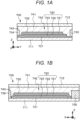
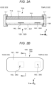
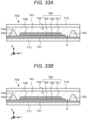
- FIG. 1A and 1B Schematic cross-sectional views of the dimming device of Example 1 are illustrated in Figs. 1A and 1B , a plan view of the first substrate and the like as viewed from the light-incident side (above) is illustrated in Fig. 2A , a plan view of the second substrate and the like as viewed from the light-incident side (above) is illustrated in Fig. 2B , a schematic cross-sectional view obtained by cutting a part of the image display device of Example 1 along an XZ plane is illustrated in Fig. 3A , a schematic view of the dimming device as viewed from the front is illustrated in Fig.
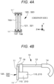
- FIG. 4A a schematic cross-sectional view obtained by cutting a part of the image display device of Example 1 along the arrow B-B in Fig. 3B (that is, cutting along a YZ plane) is illustrated in Fig. 4A , and a schematic view of the display device as viewed from the side is illustrated in Fig. 4B .
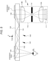
- a conceptual diagram of the image display device of Example 1 is illustrated in Fig. 5
- a schematic cross-sectional view illustrating a part of a reflection type volume hologram diffraction grating in an enlarged manner is illustrated in Fig. 6
- a schematic view of the display device of Example 1 as viewed from above is illustrated in Fig.
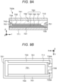
- Figs. 1A and 1B are schematic cross-sectional views of the dimming device obtained by respectively cutting the dimming device along the arrows A-A and B-B in Fig. 2A .
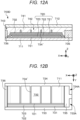
- plan views illustrated in Figs. 2A, 2B, 2C , 9B , 10B , 12B , and 13B illustrate not only the structural elements of the dimming device in the same level, but also the structural elements of the dimming device in different levels.
- An image display device 100, 200, 300, 400, 500 of Example 1 or Examples 2 to 13 described later includes:
- a display device of Example 1 or Examples 2 to 8, Examples 10 to 13 described later is more specifically a head mounted display (HMD), and includes:
- the dimming device 700 includes:
- the dimming device 700 is constituted by an optical shutter to which a color change of a substance generated by a redox reaction of an electrochromic material is applied.
- the dimming layer 720 includes an electrochromic material.
- the dimming layer 720 constituting the dimming device 700 includes an electrochromic material layer.
- the dimming layer (electrochromic material layer) 720 has a laminated structure of a reduction coloring layer 721, an electrolyte layer 722, and an oxidation coloring layer 723.
- each of the first electrode 731 and the second electrode 732 contains a transparent electrically conductive material such as ITO or IZO
- the reduction coloring layer 721 contains tungsten oxide (WO 3 )
- the electrolyte layer 722 contains tantalum oxide (Ta 2 O 5 )
- the oxidation coloring layer 723 contains iridium atoms.
- an iridium oxide (IrO x )-based material was used as a material contained in the oxidation coloring layer 723 containing iridium atoms; specifically, iridium tin oxide (Ir y Sn 1-y O x ) was used in each Example.
- y 0.5.
- the WO 3 layer reductively develops a color.
- the Ir y Sn 1-y O x layer oxidatively develops a color.
- Ir and H 2 O react with each other, and exist as iridium hydroxide Ir(OH) n . If a negative potential is applied to the first electrode 731 and a positive potential is applied to the second electrode 732, a proton H + moves from the Ir y Sn 1-y O layer to the Ta 2 O 5 layer, an electron is released to the second electrode 732, the following oxidation reaction proceeds, and the Ir y Sn 1-y O layer is colored. Ir(OH) n ⁇ IrO X (OH) n-X (colored) + X ⁇ H + + X ⁇ e
- the Ta 2 O 5 layer contains H 2 O.
- H 2 O is ionized by applying a voltage to the first electrode 731 and the second electrode 732.
- the Ta 2 O 5 layer includes a proton H + and an OH - ion, contributing to a coloring reaction and a decoloring reaction.
- the first substrate 711 and the second substrate 712 contain a plastic material. Specifically, the first substrate 711 and the second substrate 712 contain a polycarbonate resin 0.3 mm thick, for example. On an outer face of the second substrate 712, a hard coat layer (not illustrated) containing acrylic modified colloidal silica particles, phenyl ketone and acrylate organic matter, and methyl ethyl ketone is formed.
- the edge portion of the dimming device 700 is fixed (bonded) to the frame 10 (specifically, for example, rim portions 11') using an adhesive 737.
- the edge portions of light guide plates 121 and 321 described later are also fixed (bonded) to the frame 10 (specifically, the rim portions 11') using an adhesive 738.
- the adhesive 737 contains an adhesive that allows water vapor to permeate therethrough.
- optical devices 120, 320, and 520 at least partially overlap with the dimming device 700, which is a type of optical shutter. Specifically, in the example illustrated in Figs. 3A and 3B , the optical devices 120, 320, and 520 overlap with the dimming device 700. In other words, the light guide plates 121 and 321 have the same (or substantially the same) outward shape as those of the first substrate 711 and the second substrate 712. The dimming device 700 overlaps with most of the light guide plates 121 and 321.
- the configuration is not limited thereto, and the optical devices 120, 320, and 520 may also overlap with a part of the dimming device 700, or the dimming device 700 may overlap with a part of the optical devices 120, 320, and 520.
- the devices are disposed in the order of the optical device 120, 320, or 520 and the dimming device 700 from the observer side, but may also be disposed in the order of the dimming device 700 and the optical device 120, 320, or 520.
- the outward shape of the first substrate and the second substrate in Figs. 2A and 2B and the outward shape of the dimming device illustrated in Fig. 3B are displayed as different shapes, but in actuality, the dimming device has the outward shape illustrated in Fig. 3B , for example.
- a moisture-retaining member 741 is provided at least between the second electrode 732 and the second substrate 712. Then, an end surface of the moisture-retaining member 741 is exposed to the outside.
- At least part of an end section (a side surface) of the dimming device 700 includes sealing members 733, 734, 735, and 736, and a moisture-retaining member from the side of the first substrate. That is, at least part of an end section of the dimming device 700 has a stacked structure of the sealing members 733, 734, 735, and 736, and a moisture-retaining member extending portion 743 extending from the moisture-retaining member 741 from the side of the first substrate.
- the sealing members 733, 734, 735, and 736 are provided in an edge portion of the first substrate 711.
- the second electrode 732 is formed extending over from the dimming layer 720 to the first substrate 711, and also separated from the first electrode 731, while the moisture-retaining member 741 covers at least the second electrode 732 and the dimming layer 720. That is, the first electrode 731 is formed on the first substrate 711, the dimming layer 720 is formed on the first electrode 731, the second electrode 732 is formed at least on the dimming layer 720, and the moisture-retaining member 741 covers at least the second electrode 732 and faces the second substrate 712.
- the moisture-retaining member extending portion 743 extending from the moisture-retaining member 741 is provided between the sealing members 733 and 734 and the second substrate.
- sealing members 733 and 734 which are part of sealing members 733, 734, 735, and 736 are formed as auxiliary electrodes containing copper (Cu). Also, the remaining parts 735 and 736 of the sealing members 733, 734, 735, and 736 contain a resin, specifically an acrylic adhesive.
- the auxiliary electrode includes a first auxiliary electrode 733 formed on top of the first electrode 731 and a second auxiliary electrode 734 formed on top of the second electrode 732 and separated from the first auxiliary electrode 733.
- the side walls of the dimming device 700 are formed by the sealing members 733, 734, 735, and 736 as well as the moisture-retaining member extending portion 743. Also, the sealing members 733, 734, 735, and 736 are provided without gaps.
- the Young's modulus of the material (specifically, the resin) contained in the moisture-retaining member 741 and the moisture-retaining member extending portion 743 is desirably 1 ⁇ 10 6 Pa or less.
- the resin contained in the moisture-retaining member 741 and the moisture-retaining member extending portion 743 which may also be called a proton-supplying member, a transparent adhesive member capable of retaining moisture, or a transparent sealing member capable of retaining moisture, may be selected appropriately from among acrylic resins, silicone resins, and urethane resins, and for Example 1 or Examples 2 to 15 described later, an acrylic resin is contained specifically.
- the moisture-retaining member 741 and the moisture-retaining member extending portion 743 contain a material whose Young's modulus is 1 ⁇ 10 6 Pa or less, various differences in level occurring inside the dimming device can be absorbed, and inconsistencies in the thickness of the moisture-retaining member 742 in the central portion of the dimming device and inconsistencies in the thickness of the moisture-retaining member extending portion 743 can be reduced. In other words, a uniform overall distance between the first substrate and the second substrate may be attained. Furthermore, as a result, degraded visibility can be prevented. Specifically, when looking out at the external world through the dimming device 700, the occurrence of distortions or discrepancies in the image of the external world can be suppressed.
- the first electrode 731 and the second electrode 732 containing ITO are not patterned but are so-called solid electrodes.
- connectors (not illustrated) are attached to portions 733A and 734A of the auxiliary electrodes 733 and 734 of the dimming device 700, while the first electrode 731 and the second electrode 732 are electrically connected to a control circuit (specifically, a control device 18 described later) for controlling the light shielding ratio of the dimming device 700.
- the optical device 120, 320 of Example 1 or Examples 2 to 8 described later has a first structure, and includes:
- the optical device is the optical device with structure 1-B
- the image display device is the image forming device with first configuration.
- the first deflecting means and the second deflecting means are disposed on (specifically, stuck to) a surface of the light guide plate 121 (specifically, the second surface 123 of the light guide plate 121).
- the first deflecting means diffracts and reflects light incident on the light guide plate 121
- the second deflecting means diffracts and reflects light propagated by total reflection through the inside of the light guide plate 121.
- first deflecting means and the second deflecting means is constituted by a diffraction grating element, specifically a reflection type diffraction grating element, more specifically a reflection type volume hologram diffraction grating.
- first deflecting means constituted by a hologram diffraction grating is referred to as a "first diffraction grating member 130" for convenience
- second deflecting means constituted by a hologram diffraction grating is referred to as a "second diffraction grating member 140" for convenience.
- the parallel light is propagated by total reflection through the inside of the light guide plate 121 and then emitted.
- the light guide plate 121 is thin, and a path through which light travels inside the light guide plate 121 is long. Therefore, the number of times of total reflection before the light reaches the second diffraction grating member 140 differs depending on an angle of view. More specifically, in the parallel light incident on the light guide plate 121, the number of times of reflection of the parallel light incident at an angle in a direction approaching the second diffraction grating member 140 is smaller than the number of times of reflection of the parallel light incident on the light guide plate 121 at an angle in a direction away from the second diffraction grating member 140.
- the parallel light diffracted and reflected by the first diffraction grating member 130 and incident on the light guide plate 121 at an angle in a direction approaching the second diffraction grating member 140 has a smaller angle formed with the normal line of the light guide plate 121 when light propagated through the inside of the light guide plate 121 collides with an inner surface of the light guide plate 121 than the parallel light incident on the light guide plate 121 at an angle in the opposite direction thereto.
- the shape of an interference fringe formed inside the second diffraction grating member 140 and the shape of an interference fringe formed inside the first diffraction grating member 130 have a symmetrical relationship with respect to a virtual plane perpendicular to the axis of the light guide plate 121.
- a surface of each of the first diffraction grating member 130 and the second diffraction grating member 140 not facing the light guide plate 121 may be covered with a transparent resin plate or a transparent resin film, and the first diffraction grating member 130 and the second diffraction grating member 140 may be prevented from being damaged. Furthermore, a transparent protective film may be stuck to the first surface 122 to protect the light guide plate 121.
- the light guide plate 121 in Example 7 described later has the same configuration and structure as those of the above-described light guide plate 121.
- the image forming device 110 is the image forming device with first configuration and has a plurality of pixels arranged in a two-dimensional matrix.
- the image forming device 110 is constituted by an organic EL display device 111.
- An image emitted from the organic EL display device 111 passes through a first convex lens 113A constituting a lens system, further passes through a second convex lens 113B constituting the lens system, and is converted into parallel light to travel toward the light guide plate 121.
- a front focal point f 2F of the second convex lens 113B is located at a rear focal point f 1B of the first convex lens 113A.
- the frame 10 includes a front portion 11 disposed in front of the observer 20, two temple portions 13 rotatably attached to both ends of the front portion 11 via hinges 12, and a modern portion (also referred to as a leading cell, an earmuff, or an ear pad) 14 attached to a distal end portion of each of the temple portions 13. Furthermore, a nose pad 10' (refer to Fig. 8 ) is attached. In other words, basically, an assembly of the frame 10 and the nose pad 10' has substantially the same structure as that of ordinary eyeglasses. Furthermore, each casing 115 is attached to each of the temple portions 13 by an attachment member 19.
- the frame 10 is manufactured from metal or plastic. Each casing 115 may be detachably attached to each of the temple portions 13 by the attachment member 19.
- each casing 115 may be detachably attached to each of the temple portions 13 of the frame 10 of the eyeglasses owned by the observer by the attachment member 19.
- Each casing 115 may be attached to the outside or the inside of each of the temple portions 13.
- the light guide plate 121 may be fitted in the rim portion 11' included in the front portion 11.
- wiring (signal line, power supply line, or the like) 15 extending from one of the image forming devices 110, 210 extends to the outside from a distal end portion of the modern portion 14 via each of the temple portions 13 and the inside of the modern portion 14, and is connected to a control device (control circuit or control means) 18.
- Each of the image forming devices 110, 210 includes a headphone portion 16. Headphone portion wiring 16' extending from each of the image forming devices 110, 210 extends from a distal end portion of the modern portion 14 to the headphone portion 16 via each of the temple portions 13 and the inside of the modern portion 14.
- the headphone portion wiring 16' extends from a distal end portion of the modern portion 14 to the headphone portion 16 so as to go around a back side of the auricle (auditory capsule). With such a configuration, an impression that the headphone portion 16 or the headphone portion wiring 16' is disorderly disposed is not given, and a simple display device can be obtained.
- the wiring (signal line, power supply line, or the like) 15 is connected to the control device (control circuit) 18, and the control device 18 performs processing for image display.
- the control device 18 can be constituted by a well-known circuit.
- the dimming device 700 can be manufactured by the following method.
- first, the first electrode 731, the dimming layer 720, and the second electrode 732 are formed on top of the first substrate 711, and the sealing members are formed in the edge portion of the first substrate 711.
- the reduction coloring layer 721 constituted by a WO 3 layer (tungsten oxide) having a thickness of 0.49 ⁇ m is formed on the basis of a reactive sputtering method.
- the oxidation coloring layer 723, the electrolyte layer 722, and the reduction coloring layer 721 can be formed also by a magnetron sputtering method, an anodic oxidation method, a plasma CVD method, a sol-gel method, or the like.
- the oxidation coloring layer 723, the electrolyte layer 722, and the reduction coloring layer 721 may be formed using a metal mask.
- the second electrode 732 constituted by ITO having a thickness of 0.30 ⁇ m is formed on the reduction coloring layer 721.
- the first electrode 731 and the second electrode 732 can be formed on the basis of a PVD method such as an ion plating method or a vacuum vapor deposition method, a sol-gel method, or a CVD method. During film formation, the first electrode 731 and the second electrode 732 may be formed using a metal mask.
- a PVD method such as an ion plating method or a vacuum vapor deposition method, a sol-gel method, or a CVD method.
- the first electrode 731 and the second electrode 732 may be formed using a metal mask.
- the display device was stored in an environment of 60°C or higher and 30% RH or less for 1000 hours, and then a DC voltage of 1.5 V was applied between the first electrode 731 and the second electrode 732 for 30 seconds. At this time, the total light transmittance in the visible light region was reduced to 7%. Thereafter, the display device was stored in an environment of normal temperature/normal humidity for 10 hours, and then a DC voltage of 1.5 V was applied between the first electrode 731 and the second electrode 732 for 30 seconds. At this time, the total light transmittance in the visible light region was reduced to 4%. In other words, the display device recovered to an initial state.
- an image imaged by the camera 17 included in the display device may be sent to a cloud computer or a server via communication means.
- the cloud computer or the server may retrieve various kinds of information and data corresponding to the image imaged by the camera 17.
- the various kinds of information and data retrieved may be sent to the display device via the communication means.
- An image of the various kinds of information and data retrieved may be displayed on the image display device 100, 200, 300, 400, 500.
- “Information" can be displayed on the image forming device 110, 210 with higher accuracy.
- the dimming device 700 may be in an operation state all the time, may be determined to be in an operation/non-operation (ON/OFF) state by instruction (operation) of an observer, or may be normally in a non-operation state while starting operation on the basis of a signal for displaying an image in the image display device 100, 200, 300, 400, 500.
- the display device In order to determine an operation/non-operation state by instruction (operation) of an observer, for example, the display device only needs to further include a microphone via which a voice is input and the dimming device 700 is thereby controlled. Specifically, switching of operation/non-operation of the dimming device 700 only needs to be controlled according to an instruction based on a real voice of an observer.
- the light shielding ratio of the virtual image projection region of the dimming device may also be configured to increase successively over time. In other words, what is referred to as a fade in can be achieved.
- the sealing member 751 corresponding to a part of the outer wall of the dimming device 700A is formed such that there are no gaps, except for the regions corresponding to portions 733A and 734A of the auxiliary electrodes 733 and 734 where connectors are to be attached.
- the configuration and structure of the dimming device 700A of Example 2 as well as an image display device and a display device using the dimming device 700A of Example 2 may be similar to the configuration and structure of the dimming device 700, the image display device, and the display device described in Example 1, and therefore a detailed description is omitted.
- Example 7 is a modification of Example 1 to Example 6, and relates to the optical device with structure 1-B and the image forming device with second configuration.
- the image forming device 210 of Example 7 is constituted by the image forming device with second configuration.
- the image forming device 210 includes a light source 211, scanning means 212 for scanning parallel light emitted from the light source 211, and a lens system 213 for converting light emitted from the light source 211 into parallel light.
- the light source 211 is constituted by, for example, a semiconductor laser element.
- light emitted from the light source 211 is converted into parallel light by a lens (not illustrated).
- the parallel light is horizontally and vertically scanned by the scanning means 212 including a MEMS mirror that can make a micromirror rotatable in a two-dimensional direction and can scan incident parallel light two-dimensionally, and formed into a kind of two-dimensional image to generate virtual pixels (the number of pixels can be the same as, for example, that of Example 1).
- the light from the virtual pixels passes through the lens system 213 having a positive optical power, and a light flux that has been converted into parallel light is incident on the light guide plate 121.
- the optical device 120 has the same configuration and structure as those of the optical device described in Example 1. Therefore, a detailed description thereof will be omitted. Furthermore, as described above, the display device of Example 7 has substantially the same configuration and structure as those of the display device of Example 1 except for a difference in the image forming device 210. Therefore, a detailed description thereof will be omitted.
- Example 8 is a modification of Example 1 to Example 7, but relates to the optical device with structure 1-A and the image forming device with first or second configuration.
- the first deflecting means 330 and the second deflecting means 340 of Example 8 are disposed inside the light guide plate 321.
- the first deflecting means 330 reflects light incident on the light guide plate 321
- the second deflecting means 340 transmits and reflects light propagated by total reflection through the inside of the light guide plate 321 a plurality of times.
- the first deflecting means 330 functions as a reflecting mirror
- the second deflecting means 340 functions as a semi-transmissive mirror.
- the first deflecting means 330 disposed inside the light guide plate 321 is constituted by a light reflecting film (a kind of mirror) that is constituted by aluminum (Al) and reflects light incident on the light guide plate 321.
- the second deflecting means 340 disposed inside the light guide plate 321 is constituted by a multilayer laminated structure in which many dielectric laminated films are laminated.
- the dielectric laminated film includes, for example, a TiO 2 film as a high dielectric constant material and a SiO 2 film as a low dielectric constant material.
- PCT Japanese Translation Patent Publication No. 2005-521099 discloses a multilayer laminated structure in which many dielectric laminated films are laminated.
- a thin piece containing the same material as a material constituting the light guide plate 321 is sandwiched between dielectric laminated films.
- the first deflecting means 330 parallel light incident on the light guide plate 321 is reflected so as to be totally reflected inside the light guide plate 321.
- the second deflecting means 340 parallel light propagated by total reflection through the inside of the light guide plate 321 is reflected a plurality of times, and emitted from the light guide plate 321 toward the pupil 21 of the observer 20 in the state of parallel light.
- the first deflecting means 330 it is only required to perform the following. That is, by cutting out a portion 324 in which the first deflecting means 330 is to be disposed in the light guide plate 321, a slope to form the first deflecting means 330 is formed in the light guide plate 321, a light reflecting film is formed by a vacuum vapor deposition on the slope, and then the cut-out portion 324 of the light guide plate 321 is bonded to the first deflecting means 330.
- the second deflecting means 340 it is only required to perform the following.
- a multilayer laminated structure obtained by laminating many layers of the same material (for example, glass) as a material constituting the light guide plate 321 and dielectric laminated films (for example, the dielectric laminated films can be formed by a vacuum vapor deposition method) is manufactured, a portion 325 in which the second deflecting means 340 is to be disposed in the light guide plate 321 is cut out to form a slope, the multilayer laminated structure is bonded to the slope, and polishing or the like is performed to adjust an outer shape.
- the optical device 320 in which the first deflecting means 330 and the second deflecting means 340 are disposed inside the light guide plate 321 can be obtained.
- Fig. 19 illustrates a conceptual diagram of the image display device 400 in the display device (head mounted display) of Example 8.
- the image forming device 210 is constituted by the image forming device with second configuration in a similar manner to Example 7.
- the display device of Example 8 has substantially the same configuration and structure as those of the display devices of Example 1 to Example 7 except for the above difference, and therefore detailed description thereof will be omitted.
- Example 9 is a modification of the image display devices of Examples 7 and 8, and relates to the optical device with second structure and the image forming device with second configuration.
- Fig. 20 illustrates a schematic view of a display device of Example 9 as viewed from above.
- the optical device 520 constituting the image display device 500 includes a semi-transmissive mirror 530A, 530B on which light emitted from a light source is incident and from which the light is emitted toward the pupil 21 of the observer 20.
- light beams emitted from light sources 211A and 211B disposed in casings 215A and 215B are propagated through the inside of an optical fiber (not illustrated), and incident on, for example, scanning means 212A and 212B attached to the rim portion 11' in the vicinity of a nose pad, and the light beams scanned by the scanning means 212A and 212B are incident on the semi-transmissive mirrors 530A and 530B, respectively.
- light beams emitted from the respective light sources 211A and 211B disposed in the respective casings 215A and 215B are propagated through the inside of an optical fiber (not illustrated), and incident on, for example, the scanning means 212A and 212B attached above the rim portion 11' respectively corresponding to both eyes, and the light beams scanned by the scanning means 212A and 212B are incident on the semi-transmissive mirrors 530A and 530B.
- the image forming device 210A, 210B can be substantially the image forming device 210 described in Example 7.
- the display device of Example 9 has substantially the same configuration and structure as those of the display devices of Examples 7 and 8 except for the above difference, and therefore detailed description thereof will be omitted.
- Example 10 is a modification of Examples 1 to 9.
- Fig. 21A illustrates a schematic view of a display device of Example 10 as viewed from above.
- Fig. 21B illustrates a schematic diagram of a circuit for controlling an illuminance sensor.
- the display device of Example 10 further includes an environmental illuminance measuring sensor 801 for measuring the illuminance of an environment where the display device is placed, and controls the light shielding ratio of the dimming device 700 on the basis of a measurement result of the environmental illuminance measuring sensor 801. At the same time, or independently, the display device of Example 10 controls the brightness of an image formed by the image forming device 110, 210 on the basis of the measurement result of the environmental illuminance measuring sensor 801.
- the environmental illuminance measuring sensor 801 having a well-known configuration and structure only needs to be disposed, for example, at an outer end portion of the dimming device 700.
- the environmental illuminance measuring sensor 801 is connected to the control device 18 via a connector and wiring (not illustrated).
- the control device 18 includes a circuit for controlling the environmental illuminance measuring sensor 801.
- the circuit for controlling the environmental illuminance measuring sensor 801 includes an illuminance calculating circuit for receiving a measurement value from the environmental illuminance measuring sensor 801 to determine illuminance, a comparison calculating circuit for comparing an illuminance value determined by the illuminance calculating circuit with a standard value, and an environmental illuminance measuring sensor control circuit for controlling the dimming device 700 and/or the image forming device 110, 210 on the basis of the value determined by the comparison calculating circuit.
- These circuits may be constituted by well-known circuits. In control of the dimming device 700, the light shielding ratio of the dimming device 700 is controlled.
- control of the image forming device 110, 210 the brightness of an image formed by the image forming device 110, 210 is controlled.
- Control of the light shielding ratio in the dimming device 700 and control of the brightness of an image in the image forming device 110, 210 may be performed independently or with correlation.
- the light shielding ratio of the dimming device 700 is set to a predetermined value (first light shielding ratio) or more.
- first light shielding ratio a predetermined value
- second illuminance measurement value a measurement result of the environmental illuminance measuring sensor 801 becomes a predetermined value (second illuminance measurement value) or less
- the light shielding ratio of the dimming device 700 is set to a predetermined value (second light shielding ratio) or less.
- the first illuminance measurement value may be 10 lux.
- the first light shielding ratio may be any value of 99% to 70%.
- the second illuminance measurement value may be 0.01 lux.
- the second light shielding ratio may be any value of 49% to 1%.
- the environmental illuminance measuring sensor 801 in Example 10 can be applied to the display device described in Examples 7 to 9. Furthermore, in a case where the display device includes the camera 17, the environmental illuminance measuring sensor 801 can be constituted by a light receiving element for exposure measurement included in the camera 17.
- the light shielding ratio of the dimming device is controlled on the basis of a measurement result of the environmental illuminance measuring sensor
- the brightness of an image formed by the image forming device is controlled on the basis of a measurement result of the environmental illuminance measuring sensor
- the light shielding ratio of the dimming device is controlled on the basis of a measurement result of the transmitted light illuminance measuring sensor
- the brightness of an image formed by the image forming device is controlled on the basis of a measurement result of the transmitted light illuminance measuring sensor. Therefore, it is possible not only to impart a high contrast to a virtual image observed by an observer but also to optimize an observation state of a virtual image depending on the illuminance of an environment around the display device.
Landscapes
- Physics & Mathematics (AREA)
- General Physics & Mathematics (AREA)
- Engineering & Computer Science (AREA)
- Theoretical Computer Science (AREA)
- Nonlinear Science (AREA)
- Optics & Photonics (AREA)
- Chemical & Material Sciences (AREA)
- Inorganic Chemistry (AREA)
- Computer Hardware Design (AREA)
- Crystallography & Structural Chemistry (AREA)
- Human Computer Interaction (AREA)
- General Engineering & Computer Science (AREA)
- Electrochromic Elements, Electrophoresis, Or Variable Reflection Or Absorption Elements (AREA)
- Devices For Indicating Variable Information By Combining Individual Elements (AREA)
- Chemical Kinetics & Catalysis (AREA)
Claims (9)
- Dispositif de gradation (700) comprenant :un premier substrat (711) ;un second substrat (712) qui est prévu en face du premier substrat (711) et dans lequel pénètre la lumière externe ; etun corps empilé électrochromique prévu entre le premier substrat (711) et le second substrat (712),dans lequel le corps empilé électrochromique comporte une première électrode transparente (731), une couche de gradation (710) et une seconde électrode transparente (732) empilée sur un côté du premier substrat (711),la couche de gradation (710) a une structure empilée constituée d'une couche de coloration de réduction (721), d'une couche d'électrolyte (722) et d'une couche de coloration d'oxydation (723), etlorsqu'un nombre total d'atomes d'un métal adapté pour contribuer à la réaction de réduction dans un composé contenu dans la couche de coloration de réduction (721) est désigné par [Re] et qu'un nombre total d'atomes d'un métal adapté pour contribuer à la réaction d'oxydation dans un composé contenu dans la couche de coloration d'oxydation (723) est désigné par [Ox], une valeur de [Re] / [Ox] satisfaisant à 1 < [Re] / [Ox] ≤ 6,5,dans lequel la couche de coloration de réduction (721) contient WO3, la couche d'électrolyte (722) contient Ta2O5, et la couche de coloration d'oxydation (723) contient des atomes d'iridium.
- Dispositif de gradation (700) comprenant :un premier substrat (711) ;un second substrat (712) qui est prévu en face du premier substrat (711) et dans lequel pénètre la lumière externe ; etun corps empilé électrochromique prévu entre le premier substrat (711) et le second substrat (712),dans lequel le corps empilé électrochromique comporte une première électrode transparente (731), une couche de gradation (720) et une seconde électrode transparente (732) empilée sur un côté du premier substrat,la couche de gradation (720) a une structure empilée constituée d'une couche de coloration de réduction (721), d'une couche d'électrolyte (722) et d'une couche de coloration d'oxydation (723), etlorsqu'une épaisseur de la couche de coloration de réduction (721) est désignée par TRe et qu'une épaisseur de la couche de coloration d'oxydation (723) est désignée par TOx, une valeur de TRe / TOx satisfaisant à 1,0 < TRe / TOx ≤ 4,5 ;dans lequel TRe n'est pas égal à 0,48 µm et TOx n'est pas égal à 0,15 µm,dans lequel, lorsqu'une densité relative en volume de la couche de coloration de réduction (721) est désignée par LDRe, une densité relative en volume de la couche de coloration d'oxydation (723) est désignée par LDOx, un rapport entre un poids atomique d'un métal contribuant à une réaction de réduction dans un composé contenu dans la couche de coloration de réduction (721) et un poids atomique du composé contenu dans la couche de coloration de réduction (721) est désigné par αRe et un rapport entre un poids atomique d'un métal contribuant à une réaction d'oxydation dans un composé contenu dans la couche de coloration d'oxydation (723) et un poids atomique du composé contenu dans la couche de coloration d'oxydation (723) est désigné par αOX, une valeur de (TRe x LDRe x αRe) / (TOX x LDOx x αOX) se situe dans une plage prescrite ;dans lequel la densité relative en volume est une densité mesurée de la couche de coloration de réduction (721) ou de la couche de coloration d'oxydation (723) divisée par une densité dans un cas où le composé contenu dans la couche de coloration de réduction (721) ou la couche de coloration d'oxydation (723) est un cristal parfait,dans lequel 1,0 ≤ (TRe x LDRe x αRe) / (TOX x LDOx x αOx) ≤ 4,6, etdans lequel la couche de coloration de réduction (721) contient WO3, la couche d'électrolyte (722) contient Ta2O5, et la couche de coloration d'oxydation (723) contient des atomes d'iridium.
- Dispositif de gradation (700) selon la revendication 1 ou la revendication 2, dans lequel un élément de rétention d'humidité (741) est prévu au moins entre la seconde électrode (732) et le second substrat (712).
- Dispositif de gradation (700) selon la revendication 3, dans lequel une surface d'extrémité de l'élément de rétention d'humidité (741) est exposée à un extérieur.
- Dispositif de gradation (700) selon la revendication 1 ou la revendication 2, dans lequel chacun du premier substrat (711) et du second substrat (712) contient une matière plastique.
- Dispositif d'affichage d'image (100), comprenant :un dispositif de formation d'image (110) ;un dispositif optique (120) ayant une région de formation d'image virtuelle où une image virtuelle est formée sur une base de la lumière émise par le dispositif de formation d'image (110) ; etun dispositif de gradation (700) selon la revendication 1, placé en face d'au moins la région de formation d'image virtuelle et configuré pour ajuster une quantité de lumière externe incidente provenant d'un extérieur.
- Dispositif d'affichage d'image (100), comprenant :un dispositif de formation d'image (110) ;un dispositif optique (120) ayant une région de formation d'image virtuelle où une image virtuelle est formée sur une base de la lumière émise par le dispositif de formation d'image ; etun dispositif de gradation (700) selon la revendication 2, placé en face d'au moins la région de formation d'image virtuelle et configuré pour ajuster une quantité de lumière externe incidente provenant d'un extérieur.
- Dispositif d'affichage comprenant :une monture (10) conçue pour être montée sur une partie de tête d'un observateur ; etun dispositif d'affichage d'image (100) selon la revendication 6 fixé à la monture (10).
- Dispositif d'affichage comprenant :une monture (10) conçue pour être montée sur une partie de tête d'un observateur ; etun dispositif d'affichage d'image (100) selon la revendication 7 fixé à la monture (10).
Applications Claiming Priority (2)
| Application Number | Priority Date | Filing Date | Title |
|---|---|---|---|
| JP2017218918 | 2017-11-14 | ||
| PCT/JP2018/037420 WO2019097895A1 (fr) | 2017-11-14 | 2018-10-05 | Dispositif de commande de lumière, dispositif d'affichage d'image et dispositif d'affichage |
Publications (3)
| Publication Number | Publication Date |
|---|---|
| EP3712693A1 EP3712693A1 (fr) | 2020-09-23 |
| EP3712693A4 EP3712693A4 (fr) | 2020-12-30 |
| EP3712693B1 true EP3712693B1 (fr) | 2025-04-02 |
Family
ID=66540123
Family Applications (1)
| Application Number | Title | Priority Date | Filing Date |
|---|---|---|---|
| EP18877556.3A Active EP3712693B1 (fr) | 2017-11-14 | 2018-10-05 | Dispositif de commande de lumière, dispositif d'affichage d'image et dispositif d'affichage |
Country Status (6)
| Country | Link |
|---|---|
| US (1) | US20200264486A1 (fr) |
| EP (1) | EP3712693B1 (fr) |
| JP (1) | JP7230823B2 (fr) |
| KR (1) | KR102660379B1 (fr) |
| CN (1) | CN111316158B (fr) |
| WO (1) | WO2019097895A1 (fr) |
Families Citing this family (13)
| Publication number | Priority date | Publication date | Assignee | Title |
|---|---|---|---|---|
| US11772962B1 (en) * | 2022-08-04 | 2023-10-03 | Taiwan Semiconductor Manufacturing Company Ltd. | MEMS package and forming method thereof |
| WO2019220931A1 (fr) * | 2018-05-15 | 2019-11-21 | ソニー株式会社 | Dispositif d'affichage |
| CN109239955A (zh) * | 2018-11-20 | 2019-01-18 | 惠科股份有限公司 | 一种显示面板的测量方法、系统及显示装置 |
| JP7229385B2 (ja) * | 2019-10-18 | 2023-02-27 | 富士フイルム株式会社 | 画像表示装置 |
| US12374246B2 (en) * | 2020-09-17 | 2025-07-29 | Realfiction Lab Aps | 3D display |
| JP7533076B2 (ja) * | 2020-09-29 | 2024-08-14 | セイコーエプソン株式会社 | 回折光学部材および虚像表示装置 |
| GB2607672B (en) * | 2022-03-29 | 2023-06-28 | Envisics Ltd | Display system and light control film therefor |
| JP7260046B1 (ja) | 2022-09-30 | 2023-04-18 | 住友ベークライト株式会社 | エレクトロクロミックシート、積層体、眼鏡用レンズ及び眼鏡 |
| JP7260047B1 (ja) | 2022-09-30 | 2023-04-18 | 住友ベークライト株式会社 | 積層体、眼鏡用レンズ及び眼鏡 |
| JP7216864B1 (ja) | 2022-09-30 | 2023-02-01 | 住友ベークライト株式会社 | エレクトロクロミックシート、積層体、眼鏡用レンズ及び眼鏡 |
| EP4383061A1 (fr) * | 2022-12-08 | 2024-06-12 | Essilor International | Module de commande pour régler une valeur d'un paramètre d'une fonctionnalité d'un élément optique, dispositif optique, procédé mis en uvre par ordinateur et programme informatique |
| WO2024186745A1 (fr) * | 2023-03-03 | 2024-09-12 | Board Of Regents, The University Of Texas System | Interaction dynamique d'hôte et d'invité pour afficheur électrochromique durable |
| US20250164740A1 (en) * | 2023-11-21 | 2025-05-22 | Meta Platforms Technologies, Llc | Landscape display and orientation arrangement for virtual reality headsets |
Citations (1)
| Publication number | Priority date | Publication date | Assignee | Title |
|---|---|---|---|---|
| US20020076616A1 (en) * | 2000-03-21 | 2002-06-20 | Se-Hee Lee | Method of producing a durable electrochemical cell |
Family Cites Families (22)
| Publication number | Priority date | Publication date | Assignee | Title |
|---|---|---|---|---|
| JPS60121421A (ja) * | 1983-12-06 | 1985-06-28 | Citizen Watch Co Ltd | エポキシ樹脂で封止されたecd |
| JPS61241732A (ja) * | 1985-04-18 | 1986-10-28 | Nippon Kogaku Kk <Nikon> | 2色型エレクトロクロミツク素子 |
| JPS63106732A (ja) * | 1986-10-24 | 1988-05-11 | Asahi Glass Co Ltd | エレクトロクロミツク素子 |
| JPH04304796A (ja) * | 1991-04-02 | 1992-10-28 | Nec Corp | 画像交換システムにおける端末自由選択式テレビ会議方式 |
| US5798860A (en) * | 1996-01-16 | 1998-08-25 | Ppg Industries, Inc. | Iridium oxide film for electrochromic device |
| JPH09304796A (ja) * | 1996-05-15 | 1997-11-28 | Toyota Central Res & Dev Lab Inc | 全固体エレクトロクロミックセル |
| JP2000002895A (ja) * | 1998-04-14 | 2000-01-07 | Murakami Corp | 全固体型エレクトロクロミック防眩ミラーの封止構造 |
| JP2004062030A (ja) * | 2002-07-31 | 2004-02-26 | Nippon Oil Corp | エレクトロクロミック調光素子 |
| JP2004093687A (ja) * | 2002-08-29 | 2004-03-25 | Murakami Corp | エレクトロクロミック素子 |
| JP4569942B2 (ja) | 2002-09-26 | 2010-10-27 | 三菱電機株式会社 | 光アクティブデバイス |
| JP4105537B2 (ja) * | 2002-12-24 | 2008-06-25 | 株式会社村上開明堂 | エレクトロクロミック素子 |
| KR100756846B1 (ko) * | 2005-11-02 | 2007-09-07 | 주식회사 엘지화학 | 전기변색소자의 전극구조 |
| FR2899631B1 (fr) * | 2006-04-10 | 2010-02-26 | Saint Gobain | Vitrage feuillete et ses moyens d'etancheification et de renforcement peripherique |
| FR2904123B1 (fr) * | 2006-07-21 | 2008-09-12 | Saint Gobain | Dispositif electrochimique / electrocommandable du type vitrage et a proprietes optiques et/ou energetiques variables. |
| JP2008102272A (ja) * | 2006-10-18 | 2008-05-01 | Bridgestone Corp | エレクトロクロミック素子及びその製造方法 |
| JP2010014917A (ja) * | 2008-07-03 | 2010-01-21 | Bridgestone Corp | エレクトロクロミック素子及びその製造方法 |
| JP2012145814A (ja) * | 2011-01-13 | 2012-08-02 | Tokai Rika Co Ltd | エレクトロクロミックミラー |
| JP2012252091A (ja) * | 2011-06-01 | 2012-12-20 | Sony Corp | 表示装置 |
| JP6123342B2 (ja) * | 2013-02-20 | 2017-05-10 | ソニー株式会社 | 表示装置 |
| JP6892213B2 (ja) * | 2015-04-30 | 2021-06-23 | ソニーグループ株式会社 | 表示装置及び表示装置の初期設定方法 |
| KR102010755B1 (ko) * | 2016-03-22 | 2019-08-14 | 주식회사 엘지화학 | 전기변색소자, 전기변색소자의 제조방법 및 그 투과율 제어방법 |
| WO2019077920A1 (fr) * | 2017-10-17 | 2019-04-25 | ソニー株式会社 | Dispositif de gradation, dispositif d'affichage d'image, dispositif d'affichage de production de dispositif de gradation |
-
2018
- 2018-10-05 WO PCT/JP2018/037420 patent/WO2019097895A1/fr not_active Ceased
- 2018-10-05 CN CN201880072122.8A patent/CN111316158B/zh active Active
- 2018-10-05 KR KR1020207011917A patent/KR102660379B1/ko active Active
- 2018-10-05 JP JP2019553743A patent/JP7230823B2/ja active Active
- 2018-10-05 EP EP18877556.3A patent/EP3712693B1/fr active Active
- 2018-10-05 US US16/762,213 patent/US20200264486A1/en not_active Abandoned
Patent Citations (1)
| Publication number | Priority date | Publication date | Assignee | Title |
|---|---|---|---|---|
| US20020076616A1 (en) * | 2000-03-21 | 2002-06-20 | Se-Hee Lee | Method of producing a durable electrochemical cell |
Also Published As
| Publication number | Publication date |
|---|---|
| KR102660379B1 (ko) | 2024-04-23 |
| JPWO2019097895A1 (ja) | 2021-01-28 |
| EP3712693A1 (fr) | 2020-09-23 |
| EP3712693A4 (fr) | 2020-12-30 |
| CN111316158B (zh) | 2024-04-12 |
| JP7230823B2 (ja) | 2023-03-01 |
| KR20200086663A (ko) | 2020-07-17 |
| US20200264486A1 (en) | 2020-08-20 |
| CN111316158A (zh) | 2020-06-19 |
| WO2019097895A1 (fr) | 2019-05-23 |
Similar Documents
| Publication | Publication Date | Title |
|---|---|---|
| EP3712693B1 (fr) | Dispositif de commande de lumière, dispositif d'affichage d'image et dispositif d'affichage | |
| EP3486708B1 (fr) | Dispositif d'affichage d'image et dispositif d'affichage | |
| EP3699682B1 (fr) | Dispositif de gradation et production d'un dispositif de gradation | |
| US11333887B2 (en) | Optical device and display device | |
| US20240219737A1 (en) | Display device | |
| JP6468182B2 (ja) | 表示装置 | |
| JP6848865B2 (ja) | 光学装置、画像表示装置及び表示装置 | |
| CN110537136B (zh) | 光学装置、图像显示装置及显示装置 | |
| KR20210113988A (ko) | 광학 장치, 화상 표시 장치, 및 표시 장치 | |
| US20220214550A1 (en) | Image display apparatus and display apparatus |
Legal Events
| Date | Code | Title | Description |
|---|---|---|---|
| STAA | Information on the status of an ep patent application or granted ep patent |
Free format text: STATUS: THE INTERNATIONAL PUBLICATION HAS BEEN MADE |
|
| PUAI | Public reference made under article 153(3) epc to a published international application that has entered the european phase |
Free format text: ORIGINAL CODE: 0009012 |
|
| STAA | Information on the status of an ep patent application or granted ep patent |
Free format text: STATUS: REQUEST FOR EXAMINATION WAS MADE |
|
| 17P | Request for examination filed |
Effective date: 20200423 |
|
| AK | Designated contracting states |
Kind code of ref document: A1 Designated state(s): AL AT BE BG CH CY CZ DE DK EE ES FI FR GB GR HR HU IE IS IT LI LT LU LV MC MK MT NL NO PL PT RO RS SE SI SK SM TR |
|
| AX | Request for extension of the european patent |
Extension state: BA ME |
|
| A4 | Supplementary search report drawn up and despatched |
Effective date: 20201201 |
|
| RIC1 | Information provided on ipc code assigned before grant |
Ipc: G02F 1/1516 20190101ALN20201125BHEP Ipc: G02B 27/02 20060101ALN20201125BHEP Ipc: G02F 1/1524 20190101ALI20201125BHEP Ipc: G02F 1/157 20060101ALN20201125BHEP Ipc: G02F 1/153 20060101ALN20201125BHEP Ipc: G09G 3/38 20060101ALN20201125BHEP Ipc: G02F 1/15 20190101AFI20201125BHEP Ipc: G09F 9/00 20060101ALN20201125BHEP |
|
| DAV | Request for validation of the european patent (deleted) | ||
| DAX | Request for extension of the european patent (deleted) | ||
| RAP3 | Party data changed (applicant data changed or rights of an application transferred) |
Owner name: SONY GROUP CORPORATION |
|
| STAA | Information on the status of an ep patent application or granted ep patent |
Free format text: STATUS: EXAMINATION IS IN PROGRESS |
|
| 17Q | First examination report despatched |
Effective date: 20221019 |
|
| REG | Reference to a national code |
Ref country code: DE Ref legal event code: R079 Free format text: PREVIOUS MAIN CLASS: G02F0001150000 Ipc: G02F0001152400 Ref document number: 602018080813 Country of ref document: DE |
|
| GRAP | Despatch of communication of intention to grant a patent |
Free format text: ORIGINAL CODE: EPIDOSNIGR1 |
|
| STAA | Information on the status of an ep patent application or granted ep patent |
Free format text: STATUS: GRANT OF PATENT IS INTENDED |
|
| RIC1 | Information provided on ipc code assigned before grant |
Ipc: G09F 9/00 20060101ALN20241022BHEP Ipc: G02F 1/161 20060101ALN20241022BHEP Ipc: G02F 1/157 20060101ALN20241022BHEP Ipc: G02F 1/153 20060101ALN20241022BHEP Ipc: G02F 1/1516 20190101ALN20241022BHEP Ipc: G09G 5/10 20060101ALI20241022BHEP Ipc: G06F 3/147 20060101ALI20241022BHEP Ipc: G02B 27/01 20060101ALI20241022BHEP Ipc: G02F 1/155 20060101ALI20241022BHEP Ipc: G02F 1/1524 20190101AFI20241022BHEP |
|
| INTG | Intention to grant announced |
Effective date: 20241108 |
|
| GRAS | Grant fee paid |
Free format text: ORIGINAL CODE: EPIDOSNIGR3 |
|
| GRAA | (expected) grant |
Free format text: ORIGINAL CODE: 0009210 |
|
| STAA | Information on the status of an ep patent application or granted ep patent |
Free format text: STATUS: THE PATENT HAS BEEN GRANTED |
|
| P01 | Opt-out of the competence of the unified patent court (upc) registered |
Free format text: CASE NUMBER: APP_8108/2025 Effective date: 20250218 |
|
| AK | Designated contracting states |
Kind code of ref document: B1 Designated state(s): AL AT BE BG CH CY CZ DE DK EE ES FI FR GB GR HR HU IE IS IT LI LT LU LV MC MK MT NL NO PL PT RO RS SE SI SK SM TR |
|
| REG | Reference to a national code |
Ref country code: GB Ref legal event code: FG4D |
|
| REG | Reference to a national code |
Ref country code: CH Ref legal event code: EP |
|
| REG | Reference to a national code |
Ref country code: DE Ref legal event code: R096 Ref document number: 602018080813 Country of ref document: DE |
|
| REG | Reference to a national code |
Ref country code: IE Ref legal event code: FG4D |
|
| REG | Reference to a national code |
Ref country code: NL Ref legal event code: MP Effective date: 20250402 |
|
| PG25 | Lapsed in a contracting state [announced via postgrant information from national office to epo] |
Ref country code: NL Free format text: LAPSE BECAUSE OF FAILURE TO SUBMIT A TRANSLATION OF THE DESCRIPTION OR TO PAY THE FEE WITHIN THE PRESCRIBED TIME-LIMIT Effective date: 20250402 |
|
| REG | Reference to a national code |
Ref country code: AT Ref legal event code: MK05 Ref document number: 1781841 Country of ref document: AT Kind code of ref document: T Effective date: 20250402 |
|
| PG25 | Lapsed in a contracting state [announced via postgrant information from national office to epo] |
Ref country code: PT Free format text: LAPSE BECAUSE OF FAILURE TO SUBMIT A TRANSLATION OF THE DESCRIPTION OR TO PAY THE FEE WITHIN THE PRESCRIBED TIME-LIMIT Effective date: 20250804 Ref country code: ES Free format text: LAPSE BECAUSE OF FAILURE TO SUBMIT A TRANSLATION OF THE DESCRIPTION OR TO PAY THE FEE WITHIN THE PRESCRIBED TIME-LIMIT Effective date: 20250402 Ref country code: FI Free format text: LAPSE BECAUSE OF FAILURE TO SUBMIT A TRANSLATION OF THE DESCRIPTION OR TO PAY THE FEE WITHIN THE PRESCRIBED TIME-LIMIT Effective date: 20250402 |
|
| REG | Reference to a national code |
Ref country code: LT Ref legal event code: MG9D |
|
| PG25 | Lapsed in a contracting state [announced via postgrant information from national office to epo] |
Ref country code: NO Free format text: LAPSE BECAUSE OF FAILURE TO SUBMIT A TRANSLATION OF THE DESCRIPTION OR TO PAY THE FEE WITHIN THE PRESCRIBED TIME-LIMIT Effective date: 20250702 Ref country code: GR Free format text: LAPSE BECAUSE OF FAILURE TO SUBMIT A TRANSLATION OF THE DESCRIPTION OR TO PAY THE FEE WITHIN THE PRESCRIBED TIME-LIMIT Effective date: 20250703 |
|
| PG25 | Lapsed in a contracting state [announced via postgrant information from national office to epo] |
Ref country code: PL Free format text: LAPSE BECAUSE OF FAILURE TO SUBMIT A TRANSLATION OF THE DESCRIPTION OR TO PAY THE FEE WITHIN THE PRESCRIBED TIME-LIMIT Effective date: 20250402 |
|
| PG25 | Lapsed in a contracting state [announced via postgrant information from national office to epo] |
Ref country code: BG Free format text: LAPSE BECAUSE OF FAILURE TO SUBMIT A TRANSLATION OF THE DESCRIPTION OR TO PAY THE FEE WITHIN THE PRESCRIBED TIME-LIMIT Effective date: 20250402 |
|
| PG25 | Lapsed in a contracting state [announced via postgrant information from national office to epo] |
Ref country code: HR Free format text: LAPSE BECAUSE OF FAILURE TO SUBMIT A TRANSLATION OF THE DESCRIPTION OR TO PAY THE FEE WITHIN THE PRESCRIBED TIME-LIMIT Effective date: 20250402 |
|
| PG25 | Lapsed in a contracting state [announced via postgrant information from national office to epo] |
Ref country code: AT Free format text: LAPSE BECAUSE OF FAILURE TO SUBMIT A TRANSLATION OF THE DESCRIPTION OR TO PAY THE FEE WITHIN THE PRESCRIBED TIME-LIMIT Effective date: 20250402 |
|
| PGFP | Annual fee paid to national office [announced via postgrant information from national office to epo] |
Ref country code: FR Payment date: 20250924 Year of fee payment: 8 |
|
| PG25 | Lapsed in a contracting state [announced via postgrant information from national office to epo] |
Ref country code: RS Free format text: LAPSE BECAUSE OF FAILURE TO SUBMIT A TRANSLATION OF THE DESCRIPTION OR TO PAY THE FEE WITHIN THE PRESCRIBED TIME-LIMIT Effective date: 20250702 |
|
| PG25 | Lapsed in a contracting state [announced via postgrant information from national office to epo] |
Ref country code: IS Free format text: LAPSE BECAUSE OF FAILURE TO SUBMIT A TRANSLATION OF THE DESCRIPTION OR TO PAY THE FEE WITHIN THE PRESCRIBED TIME-LIMIT Effective date: 20250802 |
|
| PG25 | Lapsed in a contracting state [announced via postgrant information from national office to epo] |
Ref country code: LV Free format text: LAPSE BECAUSE OF FAILURE TO SUBMIT A TRANSLATION OF THE DESCRIPTION OR TO PAY THE FEE WITHIN THE PRESCRIBED TIME-LIMIT Effective date: 20250402 |
|
| REG | Reference to a national code |
Ref country code: DE Ref legal event code: R097 Ref document number: 602018080813 Country of ref document: DE |
|
| PGFP | Annual fee paid to national office [announced via postgrant information from national office to epo] |
Ref country code: DE Payment date: 20250923 Year of fee payment: 8 |
|
| PG25 | Lapsed in a contracting state [announced via postgrant information from national office to epo] |
Ref country code: DK Free format text: LAPSE BECAUSE OF FAILURE TO SUBMIT A TRANSLATION OF THE DESCRIPTION OR TO PAY THE FEE WITHIN THE PRESCRIBED TIME-LIMIT Effective date: 20250402 Ref country code: SM Free format text: LAPSE BECAUSE OF FAILURE TO SUBMIT A TRANSLATION OF THE DESCRIPTION OR TO PAY THE FEE WITHIN THE PRESCRIBED TIME-LIMIT Effective date: 20250402 |
|
| PG25 | Lapsed in a contracting state [announced via postgrant information from national office to epo] |
Ref country code: CZ Free format text: LAPSE BECAUSE OF FAILURE TO SUBMIT A TRANSLATION OF THE DESCRIPTION OR TO PAY THE FEE WITHIN THE PRESCRIBED TIME-LIMIT Effective date: 20250402 |
|
| PG25 | Lapsed in a contracting state [announced via postgrant information from national office to epo] |
Ref country code: EE Free format text: LAPSE BECAUSE OF FAILURE TO SUBMIT A TRANSLATION OF THE DESCRIPTION OR TO PAY THE FEE WITHIN THE PRESCRIBED TIME-LIMIT Effective date: 20250402 |
|
| PG25 | Lapsed in a contracting state [announced via postgrant information from national office to epo] |
Ref country code: SK Free format text: LAPSE BECAUSE OF FAILURE TO SUBMIT A TRANSLATION OF THE DESCRIPTION OR TO PAY THE FEE WITHIN THE PRESCRIBED TIME-LIMIT Effective date: 20250402 Ref country code: RO Free format text: LAPSE BECAUSE OF FAILURE TO SUBMIT A TRANSLATION OF THE DESCRIPTION OR TO PAY THE FEE WITHIN THE PRESCRIBED TIME-LIMIT Effective date: 20250402 |
|
| PG25 | Lapsed in a contracting state [announced via postgrant information from national office to epo] |
Ref country code: IT Free format text: LAPSE BECAUSE OF FAILURE TO SUBMIT A TRANSLATION OF THE DESCRIPTION OR TO PAY THE FEE WITHIN THE PRESCRIBED TIME-LIMIT Effective date: 20250402 |
|
| PLBE | No opposition filed within time limit |
Free format text: ORIGINAL CODE: 0009261 |
|
| STAA | Information on the status of an ep patent application or granted ep patent |
Free format text: STATUS: NO OPPOSITION FILED WITHIN TIME LIMIT |
|
| REG | Reference to a national code |
Ref country code: CH Ref legal event code: L10 Free format text: ST27 STATUS EVENT CODE: U-0-0-L10-L00 (AS PROVIDED BY THE NATIONAL OFFICE) Effective date: 20260211 |
|
| 26N | No opposition filed |
Effective date: 20260105 |