EP3596155B1 - Lithographic compositions and methods of use thereof - Google Patents
Lithographic compositions and methods of use thereof Download PDFInfo
- Publication number
- EP3596155B1 EP3596155B1 EP18711315.4A EP18711315A EP3596155B1 EP 3596155 B1 EP3596155 B1 EP 3596155B1 EP 18711315 A EP18711315 A EP 18711315A EP 3596155 B1 EP3596155 B1 EP 3596155B1
- Authority
- EP
- European Patent Office
- Prior art keywords
- composition
- polymer
- masking
- alkyl
- hardmask
- Prior art date
- Legal status (The legal status is an assumption and is not a legal conclusion. Google has not performed a legal analysis and makes no representation as to the accuracy of the status listed.)
- Active
Links
Images
Classifications
-
- C—CHEMISTRY; METALLURGY
- C08—ORGANIC MACROMOLECULAR COMPOUNDS; THEIR PREPARATION OR CHEMICAL WORKING-UP; COMPOSITIONS BASED THEREON
- C08L—COMPOSITIONS OF MACROMOLECULAR COMPOUNDS
- C08L81/00—Compositions of macromolecular compounds obtained by reactions forming in the main chain of the macromolecule a linkage containing sulfur with or without nitrogen, oxygen or carbon only; Compositions of polysulfones; Compositions of derivatives of such polymers
- C08L81/06—Polysulfones; Polyethersulfones
-
- C—CHEMISTRY; METALLURGY
- C08—ORGANIC MACROMOLECULAR COMPOUNDS; THEIR PREPARATION OR CHEMICAL WORKING-UP; COMPOSITIONS BASED THEREON
- C08G—MACROMOLECULAR COMPOUNDS OBTAINED OTHERWISE THAN BY REACTIONS ONLY INVOLVING UNSATURATED CARBON-TO-CARBON BONDS
- C08G65/00—Macromolecular compounds obtained by reactions forming an ether link in the main chain of the macromolecule
- C08G65/34—Macromolecular compounds obtained by reactions forming an ether link in the main chain of the macromolecule from hydroxy compounds or their metallic derivatives
- C08G65/38—Macromolecular compounds obtained by reactions forming an ether link in the main chain of the macromolecule from hydroxy compounds or their metallic derivatives derived from phenols
- C08G65/40—Macromolecular compounds obtained by reactions forming an ether link in the main chain of the macromolecule from hydroxy compounds or their metallic derivatives derived from phenols from phenols (I) and other compounds (II), e.g. OH-Ar-OH + X-Ar-X, where X is halogen atom, i.e. leaving group
- C08G65/4012—Other compound (II) containing a ketone group, e.g. X-Ar-C(=O)-Ar-X for polyetherketones
-
- C—CHEMISTRY; METALLURGY
- C08—ORGANIC MACROMOLECULAR COMPOUNDS; THEIR PREPARATION OR CHEMICAL WORKING-UP; COMPOSITIONS BASED THEREON
- C08G—MACROMOLECULAR COMPOUNDS OBTAINED OTHERWISE THAN BY REACTIONS ONLY INVOLVING UNSATURATED CARBON-TO-CARBON BONDS
- C08G75/00—Macromolecular compounds obtained by reactions forming a linkage containing sulfur with or without nitrogen, oxygen, or carbon in the main chain of the macromolecule
- C08G75/20—Polysulfones
- C08G75/23—Polyethersulfones
-
- C—CHEMISTRY; METALLURGY
- C08—ORGANIC MACROMOLECULAR COMPOUNDS; THEIR PREPARATION OR CHEMICAL WORKING-UP; COMPOSITIONS BASED THEREON
- C08J—WORKING-UP; GENERAL PROCESSES OF COMPOUNDING; AFTER-TREATMENT NOT COVERED BY SUBCLASSES C08B, C08C, C08F, C08G or C08H
- C08J3/00—Processes of treating or compounding macromolecular substances
- C08J3/02—Making solutions, dispersions, lattices or gels by other methods than by solution, emulsion or suspension polymerisation techniques
- C08J3/09—Making solutions, dispersions, lattices or gels by other methods than by solution, emulsion or suspension polymerisation techniques in organic liquids
-
- C—CHEMISTRY; METALLURGY
- C09—DYES; PAINTS; POLISHES; NATURAL RESINS; ADHESIVES; COMPOSITIONS NOT OTHERWISE PROVIDED FOR; APPLICATIONS OF MATERIALS NOT OTHERWISE PROVIDED FOR
- C09D—COATING COMPOSITIONS, e.g. PAINTS, VARNISHES OR LACQUERS; FILLING PASTES; CHEMICAL PAINT OR INK REMOVERS; INKS; CORRECTING FLUIDS; WOODSTAINS; PASTES OR SOLIDS FOR COLOURING OR PRINTING; USE OF MATERIALS THEREFOR
- C09D171/00—Coating compositions based on polyethers obtained by reactions forming an ether link in the main chain; Coating compositions based on derivatives of such polymers
-
- C—CHEMISTRY; METALLURGY
- C09—DYES; PAINTS; POLISHES; NATURAL RESINS; ADHESIVES; COMPOSITIONS NOT OTHERWISE PROVIDED FOR; APPLICATIONS OF MATERIALS NOT OTHERWISE PROVIDED FOR
- C09D—COATING COMPOSITIONS, e.g. PAINTS, VARNISHES OR LACQUERS; FILLING PASTES; CHEMICAL PAINT OR INK REMOVERS; INKS; CORRECTING FLUIDS; WOODSTAINS; PASTES OR SOLIDS FOR COLOURING OR PRINTING; USE OF MATERIALS THEREFOR
- C09D181/00—Coating compositions based on macromolecular compounds obtained by reactions forming in the main chain of the macromolecule a linkage containing sulfur, with or without nitrogen, oxygen, or carbon only; Coating compositions based on polysulfones; Coating compositions based on derivatives of such polymers
- C09D181/06—Polysulfones; Polyethersulfones
-
- G—PHYSICS
- G03—PHOTOGRAPHY; CINEMATOGRAPHY; ANALOGOUS TECHNIQUES USING WAVES OTHER THAN OPTICAL WAVES; ELECTROGRAPHY; HOLOGRAPHY
- G03F—PHOTOMECHANICAL PRODUCTION OF TEXTURED OR PATTERNED SURFACES, e.g. FOR PRINTING, FOR PROCESSING OF SEMICONDUCTOR DEVICES; MATERIALS THEREFOR; ORIGINALS THEREFOR; APPARATUS SPECIALLY ADAPTED THEREFOR
- G03F7/00—Photomechanical, e.g. photolithographic, production of textured or patterned surfaces, e.g. printing surfaces; Materials therefor, e.g. comprising photoresists; Apparatus specially adapted therefor
- G03F7/004—Photosensitive materials
-
- G—PHYSICS
- G03—PHOTOGRAPHY; CINEMATOGRAPHY; ANALOGOUS TECHNIQUES USING WAVES OTHER THAN OPTICAL WAVES; ELECTROGRAPHY; HOLOGRAPHY
- G03F—PHOTOMECHANICAL PRODUCTION OF TEXTURED OR PATTERNED SURFACES, e.g. FOR PRINTING, FOR PROCESSING OF SEMICONDUCTOR DEVICES; MATERIALS THEREFOR; ORIGINALS THEREFOR; APPARATUS SPECIALLY ADAPTED THEREFOR
- G03F7/00—Photomechanical, e.g. photolithographic, production of textured or patterned surfaces, e.g. printing surfaces; Materials therefor, e.g. comprising photoresists; Apparatus specially adapted therefor
- G03F7/20—Exposure; Apparatus therefor
- G03F7/2041—Exposure; Apparatus therefor in the presence of a fluid, e.g. immersion; using fluid cooling means
- G03F7/2043—Exposure; Apparatus therefor in the presence of a fluid, e.g. immersion; using fluid cooling means with the production of a chemical active agent from a fluid, e.g. an etching agent; with meterial deposition from the fluid phase, e.g. contamination resists
-
- H—ELECTRICITY
- H10—SEMICONDUCTOR DEVICES; ELECTRIC SOLID-STATE DEVICES NOT OTHERWISE PROVIDED FOR
- H10P—GENERIC PROCESSES OR APPARATUS FOR THE MANUFACTURE OR TREATMENT OF DEVICES COVERED BY CLASS H10
- H10P14/00—Formation of materials, e.g. in the shape of layers or pillars
- H10P14/60—Formation of materials, e.g. in the shape of layers or pillars of insulating materials
- H10P14/63—Formation of materials, e.g. in the shape of layers or pillars of insulating materials characterised by the formation processes
- H10P14/6326—Deposition processes
- H10P14/6342—Liquid deposition, e.g. spin-coating, sol-gel techniques or spray coating
-
- H—ELECTRICITY
- H10—SEMICONDUCTOR DEVICES; ELECTRIC SOLID-STATE DEVICES NOT OTHERWISE PROVIDED FOR
- H10P—GENERIC PROCESSES OR APPARATUS FOR THE MANUFACTURE OR TREATMENT OF DEVICES COVERED BY CLASS H10
- H10P14/00—Formation of materials, e.g. in the shape of layers or pillars
- H10P14/60—Formation of materials, e.g. in the shape of layers or pillars of insulating materials
- H10P14/69—Inorganic materials
- H10P14/692—Inorganic materials composed of oxides, glassy oxides or oxide-based glasses
- H10P14/6938—Inorganic materials composed of oxides, glassy oxides or oxide-based glasses the material containing at least one metal element, e.g. metal oxides, metal oxynitrides or metal oxycarbides
- H10P14/6939—Inorganic materials composed of oxides, glassy oxides or oxide-based glasses the material containing at least one metal element, e.g. metal oxides, metal oxynitrides or metal oxycarbides characterised by the metal
- H10P14/69394—Inorganic materials composed of oxides, glassy oxides or oxide-based glasses the material containing at least one metal element, e.g. metal oxides, metal oxynitrides or metal oxycarbides characterised by the metal the material containing titanium, e.g. TiO2
-
- H—ELECTRICITY
- H10—SEMICONDUCTOR DEVICES; ELECTRIC SOLID-STATE DEVICES NOT OTHERWISE PROVIDED FOR
- H10P—GENERIC PROCESSES OR APPARATUS FOR THE MANUFACTURE OR TREATMENT OF DEVICES COVERED BY CLASS H10
- H10P50/00—Etching of wafers, substrates or parts of devices
- H10P50/60—Wet etching
- H10P50/64—Wet etching of semiconductor materials
- H10P50/642—Chemical etching
-
- H—ELECTRICITY
- H10—SEMICONDUCTOR DEVICES; ELECTRIC SOLID-STATE DEVICES NOT OTHERWISE PROVIDED FOR
- H10P—GENERIC PROCESSES OR APPARATUS FOR THE MANUFACTURE OR TREATMENT OF DEVICES COVERED BY CLASS H10
- H10P70/00—Cleaning of wafers, substrates or parts of devices
- H10P70/50—Cleaning of wafers, substrates or parts of devices characterised by the part to be cleaned
- H10P70/54—Cleaning of wafer edges
-
- H—ELECTRICITY
- H10—SEMICONDUCTOR DEVICES; ELECTRIC SOLID-STATE DEVICES NOT OTHERWISE PROVIDED FOR
- H10P—GENERIC PROCESSES OR APPARATUS FOR THE MANUFACTURE OR TREATMENT OF DEVICES COVERED BY CLASS H10
- H10P76/00—Manufacture or treatment of masks on semiconductor bodies, e.g. by lithography or photolithography
- H10P76/40—Manufacture or treatment of masks on semiconductor bodies, e.g. by lithography or photolithography of masks comprising inorganic materials
- H10P76/405—Manufacture or treatment of masks on semiconductor bodies, e.g. by lithography or photolithography of masks comprising inorganic materials characterised by their composition, e.g. multilayer masks
-
- H—ELECTRICITY
- H10—SEMICONDUCTOR DEVICES; ELECTRIC SOLID-STATE DEVICES NOT OTHERWISE PROVIDED FOR
- H10P—GENERIC PROCESSES OR APPARATUS FOR THE MANUFACTURE OR TREATMENT OF DEVICES COVERED BY CLASS H10
- H10P95/00—Generic processes or apparatus for manufacture or treatments not covered by the other groups of this subclass
- H10P95/90—Thermal treatments, e.g. annealing or sintering
Definitions
- the present invention relates to compositions and methods useful for the manufacture or treatment of substrates or semiconductor devices and, in particular, to compositions and methods useful for forming layers or masks on lithographic substrates or semiconductor devices.
- antireflective layers and hardmasks are used in advanced lithographic patterning processes.
- underlayers and/or antireflective coatings for the photoresist that act as a hardmask and are highly etch resistant during substrate etching are preferred.
- One approach has been to incorporate silicon, titanium, zirconium, aluminum, or other metallic materials into a layer beneath the organic photoresist layer.
- another high carbon content antireflective or mask layer may be placed beneath the metal containing antireflective layer, to create a trilayer of high carbon film/hard mask film/photoresist.
- Such layers can be used to improve the lithographic performance of the imaging process.
- metal contamination in the lithographic and etch tools, as well as cross contamination between wafers during manufacturing should be avoided.
- Iwao et al One process and apparatus for reducing metal contamination during the manufacture of integrated circuit components has been described in US Patent No. 8,791,030 (Iwao et al ).
- a masking composition is supplied to an edge of the substrate and baked to form a masking film at the edge of the substrate.
- a hardmask composition is then coated on the substrate and the masking film.
- the portion of the hardmask composition overlying the masking film is removed using an edge bead remover and the hardmask composition is baked to form a hardmask.
- the masking film is then removed with a masking film removing solution. The result is a hardmask that is spaced from the edge of the substrate, thereby reducing contamination.
- JP 2008 015223 A relates to a resist underlay film forming composition containing polysulfones.
- the polysulfone of Example 1 has a molecular weight of 5,100.
- the polysulfone of Example 2 has a molecular weight of 22,800.
- US 5 234 990 A relates to polymers with intrinsic light-absorbing properties for antireflective coating applications in deep ultraviolet microlithography.
- the polysulfone employed can have an average molecular weight of 103 to 106, see column 7, lines 39 to 41.
- One example of a polymer is Amoco Udel ® polysulfone, see column 7, lines 47 to 52.
- Example 1 refers to this polysulfone. However, no exact molecular weight is given.
- US 5 578 676 A relates to a method for making polymers with intrinsic light-absorbing properties.
- the compositions can contain a polysulfone having an average molecular weight of 10 3 to 106, see column 7, lines 17 to 20.
- An example is Amoco Udel ® polysulfone, see column 7, lines 26 to 45. This polysulfone is also employed according to Example 1. A specific molecular weight is not given in the example.
- JP 2009 142799 A relates to a porous membrane and its manufacturing method.
- the polysulfone disclosed has a weight average molecular weight of 1,000 to 100,000, preferably 3,000 to 50,000, more preferably 5,000 to 30,000, see paragraph [0027].
- Comparative Example 3 again the Udel polysulfone is employed.
- US 6 420 514 B1 relates to transparent polysulfone articles with reduced spurious coloration.
- the reference discloses polysulfones having a weight average molecular weight of at least about 10,000, preferably at least about 25,000, more preferably at least about 35,000, and most preferably up to about 200,000 or more, see column 2, lines 35 to 40.
- Specific polysulfone resins have an average molecular weight of 20,000 to 200,000, see column 3, lines 47 to 54.
- a 15 to 40 wt% solution of a polysulfone resin having a weight average molecular weight of approximately 60,000 is furthermore disclosed, see column 4, lines 7 to 11.
- the masking compositions should produce masking films that do not significantly dissolve in the solvent used in the hardmask composition. Further, the masking films should not significantly dissolve in the edge bead remover. Even further, the masking films should be able to be removed without deleteriously affecting the hardmask. In particular, it would be useful for the masking films to be able to be removed by wet etching using a solvent that does not deleteriously affect the hardmask. In addition, it would be useful for the masking films to be able to be removed at a rate that enables commercially acceptable process times. The present disclosure addresses these needs.
- the present invention relates to a masking composition for forming a masking film comprising:
- the present invention relates to a method of manufacturing an electronic device comprising the steps of:
- the method comprises the steps of:
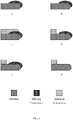
- FIG. 1a-f shows a schematic representation of one embodiment of a process for using the masking compositions of the present invention.
- a masking composition is applied onto an edge of a substrate.
- the masking composition is heated to form a masking film.
- a hardmask composition is applied onto the substrate and the masking film.
- the hardmask composition is rinsed with an edge bead remover to remove at least a portion of the hardmask composition that is in contact with the masking film.
- the hardmask composition is heated to form a hardmask. In FIG. If, the masking film is removed.
- C x-y designates the number of carbon atoms in a chain.
- C 1-6 alkyl refers to an alkyl chain having a chain of between 1 and 6 carbons (e.g. , methyl, ethyl, propyl, butyl, pentyl and hexyl). Unless specifically stated otherwise, the chain can be linear or branched.
- alkyl refers to hydrocarbon groups which can be linear, branched ( e.g., methyl, ethyl, propyl, isopropyl, tert-butyl and the like), cyclic (e.g., cyclohexyl, cyclopropyl, cyclopentyl and the like) or multicyclic (e.g., norbornyl, adamantly and the like). These alkyl moieties may be substituted or unsubstituted.
- Fluorinated alkyl refers to a linear, cyclic or branched saturated alkyl group as defined above in which one or more of the hydrogens have been replaced by fluorine (e.g. , trifluoromethyl, pefluoroethyl, 2,2,2-trifluoroethyl, prefluoroisopropyl, perfluorocyclohexyl and the like).
- fluorine e.g. , trifluoromethyl, pefluoroethyl, 2,2,2-trifluoroethyl, prefluoroisopropyl, perfluorocyclohexyl and the like.
- Alkoxy refers to an alkyl group as defined above which is attached through an oxy (-O-) moiety (e.g. , methoxy, ethoxy, propoxy, butoxy, 1,2-isopropoxy, cyclopentyloxy, cyclohexyloxy and the like). These alkoxy moieties may be substituted or unsubstituted.
- Halo or halide refers to a halogen (e.g., F, Cl, Br, and I).
- Hydroxy refers to an -OH group.
- substituted when referring to an alkyl, alkoxy, fluorinated alkyl, and the like refers to one of these moieties which also contain one or more substituents, selected from the group consisting of unsubstituted alkyl, substituted alkyl, unsubstituted aryl, substituted aryl, alkyloxy, alkylaryl, haloalkyl, halide, hydroxy, amino and amino alkyl.
- unsubstituted refers to these same moieties wherein no substituents apart from hydrogen are present.
- the masking compositions of the present invention are formed by a polymer and an organic solvent, wherein the polymer has a unit having structure (I):
- each R 1 is independently H, halo, (C 1-3 ) alkyl, (C 1-3 ) fluorinated alkyl, hydroxy, (C 1-3 ) alkoxy, or (C 1-3 ) alkyl carbonyl.
- each R 1 is independently H, F, or (C 1-3 ) alkyl.
- q is 0. In a further variation, q is 1. In another variation, q is 2. In still another variation, q is 3. In yet another variation, q is 4.
- each R 2 is independently H, halo, (C 1-3 ) alkyl, (C 1-3 ) fluorinated alkyl, hydroxy, (C 1-3 ) alkoxy, or (C 1-3 ) alkyl carbonyl.
- each R 2 is independently H, F, or (C 1-3 ) alkyl.
- r is 0. In a further variation, r is 1. In another variation, r is 2. In still another variation, r is 3. In yet another variation, r is 4.
- A can be a direct bond.
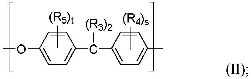
- A can have structure (II):
- each R 3 is independently H, halo, (C 1-3 ) alkyl, (C 1-3 ) fluorinated alkyl, hydroxy, (C 1-3 ) alkoxy, or (C 1-3 ) alkyl carbonyl.
- each R 3 is independently H, F, (C 1-3 ) alkyl, or (C 1-3 ) fluorinated alkyl.
- each R 4 is independently H, halo, (C 1-3 ) alkyl, (C 1-3 ) fluorinated alkyl, hydroxy, (C 1-3 ) alkoxy, or (C 1-3 ) alkyl carbonyl.
- each R 4 is independently H, F, or (C 1-3 ) alkyl.
- s is 0. In a further variation, s is 1. In another variation, s is 2. In still another variation, s is 3. In yet another variation, s is 4.
- each R 5 is independently H, halo, (C 1-3 ) alkyl, (C 1-3 ) fluorinated alkyl, hydroxy, (C 1-3 ) alkoxy, or (C 1-3 ) alkyl carbonyl.
- each R 5 is independently H, F, or (C 1-3 ) alkyl.
- t is 0. In a further variation, t is 1. In another variation, t is 2. In still another variation, t is 3. In yet another variation, t is 4.
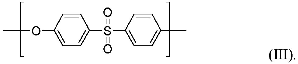
- the polymer has structure (III):
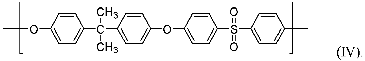
- the polymer has structure (IV):
- the polymer has structure (V):
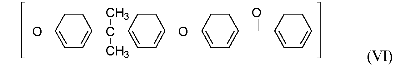
- the polymer has structure (VI):
- the molecular weight of the polymer can be selected to provide the desired etch rate. Toward that end, incorporation of polymers having low molecular weights will increase the etch rate. In this manner, the typically long etch times needed to process masking films which contain only polymers having high molecular weights can be beneficially reduced. Accordingly, a masking composition for forming a masking film comprising:
- the polymer has an average molecular weight of at least 10000. In another embodiment, the polymer has an average molecular weight of at least 20000. In a further embodiment, the polymer has an average molecular weight of at least 28000. Preferably, the polymer has an average molecular weight of between 20000 and 40000, more preferably of between 28000 and 35000.
- the composition comprises a mixture of polymers.
- the mixture of polymers comprises a first polymer having an average molecular weight greater than 30000 and a second polymer having an average molecular weight less than 30000.
- the first polymer can be obtained from Aldrich and the second polymer can be synthesized.
- Both the first polymer and the second polymer have a unit having structure (I).
- the organic solvent can be anisole, cyclohexanone, gamma butyro lactone (GBL), N-methyl-2-pyrrolidone, di-(C 1-6 ) alkyl ketones, (C 1-6 ) alkyl acetates or mixtures thereof.
- di-(C 1-6 ) alkyl ketones include, but are not limited to, butanone, cyclopentanone, ethyl isopropyl ketone, 2-hexanone, methyl isobutyl ketone, methyl isopropyl ketone, 3-methyl-2-pentanone, 2-pentanone, 3-pentanone and mixtures thereof.
- C 1-6 alkyl acetates include, but are not limited to, methyl acetate, ethyl acetate, n-propyl acetate, isopropyl acetate, n-butyl acetate, isobutyl acetate and mixtures thereof.
- the solid content in the composition can be adjusted based on the desired film thickness.
- the polymer is present in the composition in an amount of at least 0.1 wt%. In other variations, the polymer is present in an amount of at least 3 wt%. In certain variations, the polymer is present in an amount of not more than 20 wt%. In other variations, the polymer is present in an amount of not more than 15 wt%.
- the masking compositions of the present invention can be used to form a masking film in a variety of lithographic applications.
- the masking compositions of the present invention can be used to form an edge protecting layer.
- the masking composition can be applied onto an edge of a substrate and then treated to form the masking film.
- the masking compositions can be cured at a temperature between 150°C and 350°C and for a time between 60 s and 120 s.
- the masking composition can be applied to the substrate using any of a variety of techniques known in the art.
- the masking composition can be applied onto the substrate by a spin-on coating process.
- the masking compositions of the present invention can be used in a method of manufacturing an electronic device.
- a masking composition is applied onto an edge of a substrate ( FIG. 1a ) and treated (e.g., by the application of heat) to form a masking film ( FIG. 1b ).
- the masking composition can optionally be treated to reduce impurities prior to application.
- the masking composition can be treated to reduce trace metal by ion exchange.
- a hardmask composition is then applied onto the substrate and the masking film ( FIG. 1c ).
- the masking film and hardmask composition are rinsed with an edge bead remover to remove at least a portion of the hardmask composition that is in contact with the masking film ( FIG.
- a portion or portions of the hardmask composition that are in contact with the masking film may remain even after rinsing, provided that the portions that remain do not significantly reduce the effectiveness of the masking layer. For example, up to about 5% of the hardmask composition that is inn contact with the masking film may remain after rinsing.
- the hardmask composition is then treated (e.g., by the application of heat) to form a hardmask ( FIG. 1e ).
- the masking film can then be removed, leaving the hardmask spaced from the edge of the substrate (FIG. If).
- the masking composition can be applied onto the substrate using any of a variety of techniques that enables the masking composition to be applied onto an edge of the substrate.
- One technique for applying the masking composition using a spin-on coating process is described in US Patent No. 8,791,030 (Iwao et al. ) .
- the masking composition is applied in a thickness of at least 10nm, at least 50nm, at least 100nm, at least 200nm, or at least 300nm.
- the masking composition is applied in a thickness of up to 1000nm, up to 900nm, or up to 800nm.
- the masking composition is applied at a width of at least 0.5mm, or at least 0.75mm.
- the masking composition is applied at a width of not more than 1.5mm, or not more than 1.0mm.
- the masking composition is positioned to cover the edge of the substrate and to extend over the side and/or backside of the substrate.
- the masking composition can be treated to form the masking film using any of a variety of techniques.
- the masking film can be heated at a temperature between 150°C and 350°C and for a time between 60 s and 120 s.
- the hardmask composition is a metal hardmask composition.
- the hardmask composition can be a metal oxide photoresist composition.
- Suitable metal hardmask and metal oxide photoresist compositions include, but are not limited to, those described in US Patent Nos. 9,315,636 ; 8,568,958 , 9,201,305 ; 9,296,922 ; 9,409,793 ; and 9,499,698 and US Patent Application Nos. 62/437,449 (filed December 21, 2016 ) and 14/978,232 (filed December 22, 2015 ).
- suitable techniques include, but are not limited to, spin-on coating, chemical vapor deposition (CVD) and atomic layer deposition (ALD).
- CVD chemical vapor deposition
- ALD atomic layer deposition
- suitable casting solvents for the hardmask composition include, but is not limited to, PGMEA, PGME, ethyl lactate, methoxyethanol, ethoxypropanol, ethoxyethanol, 1-pentanol, 4-methyl-2-pentanol and mixtures thereof.
- any of a variety of techniques can be used to remove a portion of the hardmask composition that is in contact with the masking film. It would be understood by those skilled in the art that removal of a portion of the hardmask composition that is in contact with the masking film should not deleteriously affect that part of the hardmask composition that is not in contact with the masking film. Suitable techniques include, but are not limited to chemical mechanical polishing (CMP), plasma etching, and wet etching. When wet etching is utilized, any of a variety of solvents (such as edge bead removers) can be used provided that the solvent does not deleteriously affect the masking film or hardmask composition.
- CMP chemical mechanical polishing
- plasma etching plasma etching
- wet etching any of a variety of solvents (such as edge bead removers) can be used provided that the solvent does not deleteriously affect the masking film or hardmask composition.
- Suitable edge bead removers include, but are not limited to, PGMEA, PGME, ethyl lactate, methoxyethanol, ethoxypropanol, ethoxyethanol, 1-pentanol, 4-methyl-2-pentanol and mixtures thereof.
- the hardmask composition can be treated by a variety of techniques to form the hardmask.
- the hardmask composition can be treated by heating at a temperature between 150°C and 450°C and for a time between 60 s and 120 s.
- Suitable techniques include, but are not limited to plasma etching, and wet etching.
- wet etching any of a variety of solvents can be used provided that the solvent does not deleteriously affect the hardmask.
- Suitable solvents include, but are not limited to, anisole, cyclohexanone, gamma butyro lactone (GBL), N-methyl-2-pyrrolidone, di-(C 1-6 ) alkyl ketones, (C 1-6 ) alkyl acetates, aromatic hydrocarbons and mixtures thereof.
- Typical electronic devices that can be manufactured using the compositions and methods of the present invention include, but are not limited to computer chips, integrated circuits, and semiconductor devices.
- Bisphenol A 45.60 g, 0.20 mol
- bis(p-chlorophenyl) sulfone 57.4g, 0.20 mol
- dried potassium carbonate 55.3 g, 0.40mol
- 50 ml of toluene were placed in a 2L, 4 necked round bottom flask, fitted with a condenser, a nitrogen sweep, a Dean Stark trap (filled with toluene) and an overhead mechanical stirrer. The mixture was mixed at room temperature for 10 minutes.
- the reaction mixture was heated at 150°C for 9.5 hours on a heating mantle. The reaction mixture was then cooled to less than 50°C and filtered through filter paper. The filtered solution (pH 9 to 10) was neutralized with 10% HCl to pH 7-6, and then poured into DI water (3200 mL) in a 5L flask. A precipitate was formed. The mixture was mixed for 30 minutes and allowed to settle overnight. Water was decanted (3400 mL) and one liter THF was added to the sticky solid. After mixing, it was transferred to a beaker and heated on a hot plate to reduce volume to one liter. The polymer was precipitated by drowning the solution into 12 liter of hexane, mixing for 1 hour, and then letting the solids settle.
- the proton NMR spectrum shows peaks at 1.7 ppm due to the aliphatic group of isopropylidene group of bisphenol-A, and at 6-7.8 ppm corresponding to the aromatic protons.
- Bisphenol A (22.8g, 0.10 mole), 4,4'-Difluorobenzophenone (21.8g, 0.10 mole), potassium carbonate (27.6g, 0.20 mole), 157mL dimethylaceamide, and 21.4mL toluene was placed into a 500mL, 4 neck, round bottom flask equipped with stirring, a condenser, a thermowatch, a dean stark trap filled with toluene, and nitrogen purge.
- the solution was mixed at room temp for 10 minutes, and then the temp was set to 150°C. Since rflux begins at 147°C, the solution was held at reflux for 90 minutes. The solution was then cooled to ⁇ 70°C.
- the reaction solution was filtered to remove salts, and the filtrate was then neutralized using a small amount of 10% HCl.
- the polymer was precipitated by drowning the solution into 1600mL of DI water, mixing for 1 hour, and then letting the solids settle.
- Bisphenol A (22.8g, 0.10 mole), 4,4'-Difluorobenzophenone (21.8g, 0.10 mole), potassium carbonate (27.6g, 0.20 mole), 200mL dimethylacetamide, and 27.5mL toluene was placed into a 500mL, 4 neck, round bottom flask equipped with stirring, condenser, thermowatch, dean stark trap filled with toluene, and nitrogen purge.
- the solution was mixed at room temp for 10 minutes, and then the temperature was set to 150°C. Since reflux begins at 147°C, the solution was held at reflux for 90 minutes.
- the solution was then cooled to ⁇ 70°C, filtered to remove salts, and the filtrate was then neutralize using a small amount of 10% HCl.
- the polymer was precipitated by drowning into 1600mL of DI water, mixing for 1 hour, and then letting the solids settle.
- Process Example 1 was prepared by dissolving 1% of the polysulfone (PSU) in anisole.
- Process Example 2 was prepared by dissolving 1% of the polyethersulfone (PES) in gamma butyro lactone (GBL).
- the masking compositions were spin coated on the edge of a wafer and baked at either 250 or 350°C for 60s to form uniform films, in accordance with the technique described in US Patent No. 8,791,030 (Iwao et al ).
- the wet etch rates of masking films formed from Example 1 were investigated in various wet etchants.
- the film thickness of the masking films were measured using a Nanospec 9200 and plotted as a function of soaking time of the coated wafers.
- the etch rates were calculated as the slope of the linear regressions.
- Table 2 show that the polysulfone film can be removed rapidly with a baking temperature at 250°C using Fab friendly solvents.
- Anisole, GBL, GBL/nBA 70:30 and NMP show faster wet etch rates than cyclohexanone for the Polysulfone film.
- Table 2 Solvent Wet Etch Rate ( ⁇ )/sec Cyclohexanone 81.50 Anisole 156.83 GBL 148.97 GBL/nBA 70:30 154.47 NMP 151.37
- the wet etch rates of masking films formed from Example 1 were investigated as a function of the average molecular weight of the polysulfone.
- the film thicknesses and etch rates were determined as described above.
- the data in Table 4 demonstrate that the wet etch rates can be controlled by varying the molecular weight of the Polysulfone. Specifically, lower molecular weight Polysulfones show faster wet etch rates in cyclohexanone while retaining low etch rates in ArF thinner solvent, which is beneficial for the throughput of the Polysulfone film removal process.
- the data in table 5 show that the metal contamination in the hardmask film is reduced in the wafer treated with the masking film as compared to the wafer that was not treated with the masking film.
- Process example 3 was prepared by dissolving 567.26g of polysulfone (obtained from Aldrich, CAS 25135-51-7 ) and 402.74g of the low Mw polysulfone from synthesis example 1 in 8730g of anisole.
- Process example 4 was prepared by dissolving 21.170g of the polymer from synthesis example 2 and 28.830g of polymer from synthesis example 3 in 450.00g of anisole.
- Example 3 was repeated with polysulfone (obtained from Aldrich, CAS 25135-51-7 ) only, and the masking composition was spin coated on a silicon wafer and baked at 250°C. Then it was soaked in either ArF Thinner or cyclohexanone. The film thickness (FT) was measured before and after soak. The results are shown in Table 8.
- Table 8 Example Soak Solvent FT Before Soak ( ⁇ ) FT After Soak ( ⁇ ) Film Loss ( ⁇ ) Wet Etch Rate ⁇ /sec Process
- ArF Thinner 4923 5963 -40 -0.667 Process Example 5 Cyclohexanone 4998 618 4280 87.38
Landscapes
- Chemical & Material Sciences (AREA)
- Chemical Kinetics & Catalysis (AREA)
- Organic Chemistry (AREA)
- Health & Medical Sciences (AREA)
- Medicinal Chemistry (AREA)
- Polymers & Plastics (AREA)
- Life Sciences & Earth Sciences (AREA)
- Engineering & Computer Science (AREA)
- Materials Engineering (AREA)
- Wood Science & Technology (AREA)
- General Physics & Mathematics (AREA)
- Physics & Mathematics (AREA)
- General Chemical & Material Sciences (AREA)
- Dispersion Chemistry (AREA)
- Compositions Of Macromolecular Compounds (AREA)
- Photosensitive Polymer And Photoresist Processing (AREA)
- Internal Circuitry In Semiconductor Integrated Circuit Devices (AREA)
- Paints Or Removers (AREA)
- Cleaning Or Drying Semiconductors (AREA)
- Materials For Photolithography (AREA)
- Exposure Of Semiconductors, Excluding Electron Or Ion Beam Exposure (AREA)
- Macromonomer-Based Addition Polymer (AREA)
Description
- The present invention relates to compositions and methods useful for the manufacture or treatment of substrates or semiconductor devices and, in particular, to compositions and methods useful for forming layers or masks on lithographic substrates or semiconductor devices.
- Multiple antireflective layers and hardmasks are used in advanced lithographic patterning processes. For example, in cases where a photoresist does not provide sufficient dry etch resistance, underlayers and/or antireflective coatings for the photoresist that act as a hardmask and are highly etch resistant during substrate etching are preferred. One approach has been to incorporate silicon, titanium, zirconium, aluminum, or other metallic materials into a layer beneath the organic photoresist layer. Additionally, another high carbon content antireflective or mask layer may be placed beneath the metal containing antireflective layer, to create a trilayer of high carbon film/hard mask film/photoresist. Such layers can be used to improve the lithographic performance of the imaging process. However, metal contamination in the lithographic and etch tools, as well as cross contamination between wafers during manufacturing, should be avoided.
- One process and apparatus for reducing metal contamination during the manufacture of integrated circuit components has been described in
US Patent No. 8,791,030 (Iwao et al ). According to Iwao et al., a masking composition is supplied to an edge of the substrate and baked to form a masking film at the edge of the substrate. A hardmask composition is then coated on the substrate and the masking film. The portion of the hardmask composition overlying the masking film is removed using an edge bead remover and the hardmask composition is baked to form a hardmask. The masking film is then removed with a masking film removing solution. The result is a hardmask that is spaced from the edge of the substrate, thereby reducing contamination. -
JP 2008 015223 A -
US 5 234 990 A relates to polymers with intrinsic light-absorbing properties for antireflective coating applications in deep ultraviolet microlithography. The polysulfone employed can have an average molecular weight of 103 to 106, see column 7, lines 39 to 41. One example of a polymer is Amoco Udel® polysulfone, see column 7, lines 47 to 52. Example 1 refers to this polysulfone. However, no exact molecular weight is given. -
US 5 578 676 A relates to a method for making polymers with intrinsic light-absorbing properties. The compositions can contain a polysulfone having an average molecular weight of 103 to 106, see column 7, lines 17 to 20. An example is Amoco Udel® polysulfone, see column 7, lines 26 to 45. This polysulfone is also employed according to Example 1. A specific molecular weight is not given in the example. -
JP 2009 142799 A -
US 6 420 514 B1 relates to transparent polysulfone articles with reduced spurious coloration. The reference discloses polysulfones having a weight average molecular weight of at least about 10,000, preferably at least about 25,000, more preferably at least about 35,000, and most preferably up to about 200,000 or more, see column 2, lines 35 to 40. Specific polysulfone resins have an average molecular weight of 20,000 to 200,000, see column 3, lines 47 to 54. A 15 to 40 wt% solution of a polysulfone resin having a weight average molecular weight of approximately 60,000 is furthermore disclosed, see column 4, lines 7 to 11. - Accordingly, there is a need for masking compositions that can be supplied to an edge of a substrate and treated to form a masking film. In particular, it would be advantageous to provide masking compositions with properties that enable the solutions to be cast onto an edge of a substrate using, for example, spin on techniques. In addition, the masking compositions should produce masking films that do not significantly dissolve in the solvent used in the hardmask composition. Further, the masking films should not significantly dissolve in the edge bead remover. Even further, the masking films should be able to be removed without deleteriously affecting the hardmask. In particular, it would be useful for the masking films to be able to be removed by wet etching using a solvent that does not deleteriously affect the hardmask. In addition, it would be useful for the masking films to be able to be removed at a rate that enables commercially acceptable process times. The present disclosure addresses these needs.
- In one of its aspects, the present invention relates to a masking composition for forming a masking film comprising:
- a. a polymer comprising a unit having structure (I):

- X is selected from the group consisting of -SO2-, -C(=O)- and -O-;
- A is a direct bond or A is selected from the group consisting of structure (II):

- R1, R2, R3, R4 and R5 are each independently selected from the group consisting of H, halo, (C1-3) alkyl, (C1-3) fluorinated alkyl, hydroxy, (C1-3) alkoxy, and (C1-3) alkyl carbonyl; and
- q, r, s and t are each independently selected from the group consisting of 0, 1, 2, 3 and 4; and
- b. an organic solvent,
- In another of its aspects, the present invention relates to a method of manufacturing an electronic device comprising the steps of:
- a. applying the masking composition of any one of claims 1-8 onto an edge of a substrate; and
- b. heating the masking composition at a temperature between 150°C and 350°C and for a time between 60 s and 120 s to form a masking film.
- Preferably, the method comprises the steps of:
- a. applying the masking composition of any of claims 1-8 onto an edge of a substrate
- b. heating the masking composition at a temperature between 150°C and 350°C and for a time between 60 s and 120 s to form a masking film;
- c. applying a hardmask composition onto the substrate and the masking film;
- d. rinsing the hardmask composition with an edge bead remover to remove at least a portion of the hardmask composition that is in contact with the masking film;
- e. heating the hardmask composition to form a hardmask; and
- f. removing the masking film.
-
FIG. 1a-f shows a schematic representation of one embodiment of a process for using the masking compositions of the present invention. InFIG. 1a , a masking composition is applied onto an edge of a substrate. InFIG. 1b , the masking composition is heated to form a masking film. InFIG. 1c , a hardmask composition is applied onto the substrate and the masking film. InFIG. 1d , the hardmask composition is rinsed with an edge bead remover to remove at least a portion of the hardmask composition that is in contact with the masking film. InFIG. 1e , the hardmask composition is heated to form a hardmask. In FIG. If, the masking film is removed. - Unless otherwise stated, the following terms used in the specification and claims shall have the following meanings for the purpose of this Application.
- As used herein, "Cx-y" designates the number of carbon atoms in a chain. For example, C1-6 alkyl refers to an alkyl chain having a chain of between 1 and 6 carbons (e.g., methyl, ethyl, propyl, butyl, pentyl and hexyl). Unless specifically stated otherwise, the chain can be linear or branched.
- Unless otherwise indicated, alkyl refers to hydrocarbon groups which can be linear, branched (e.g., methyl, ethyl, propyl, isopropyl, tert-butyl and the like), cyclic (e.g., cyclohexyl, cyclopropyl, cyclopentyl and the like) or multicyclic (e.g., norbornyl, adamantly and the like). These alkyl moieties may be substituted or unsubstituted.
- Fluorinated alkyl (a.k.a. Fluoroalkyl) refers to a linear, cyclic or branched saturated alkyl group as defined above in which one or more of the hydrogens have been replaced by fluorine (e.g., trifluoromethyl, pefluoroethyl, 2,2,2-trifluoroethyl, prefluoroisopropyl, perfluorocyclohexyl and the like). These fluoroalkyl moieties, if not perfluorinated, may be unsubstituted or further substituted.
- Alkoxy (a.k.a. Alkyloxy) refers to an alkyl group as defined above which is attached through an oxy (-O-) moiety (e.g., methoxy, ethoxy, propoxy, butoxy, 1,2-isopropoxy, cyclopentyloxy, cyclohexyloxy and the like). These alkoxy moieties may be substituted or unsubstituted.
- Alkyl carbonyl refers to an alkyl group as defined above which is attached through a carbonyl group (-C(=O-)) moiety (e.g., methylcarbonyl, ethylcarbonyl, propylcarbonyl, buttylcarbonyl, cyclopentylcarbonyl and the like). These alkyl carbonyl moieties may be substituted or unsubstituted.
- Halo or halide refers to a halogen (e.g., F, Cl, Br, and I).
- Hydroxy (a.k.a. Hydroxyl) refers to an -OH group.
- Unless otherwise indicated, the term "substituted" when referring to an alkyl, alkoxy, fluorinated alkyl, and the like refers to one of these moieties which also contain one or more substituents, selected from the group consisting of unsubstituted alkyl, substituted alkyl, unsubstituted aryl, substituted aryl, alkyloxy, alkylaryl, haloalkyl, halide, hydroxy, amino and amino alkyl. Similarly, the term "unsubstituted" refers to these same moieties wherein no substituents apart from hydrogen are present.
- The masking compositions of the present invention are formed by a polymer and an organic solvent, wherein the polymer has a unit having structure (I):

- In one embodiment, X is -SO2-. In a further embodiment, X is -C(=O)-. In another embodiment, X is -O-.
- In structure (I), each R1 is independently H, halo, (C1-3) alkyl, (C1-3) fluorinated alkyl, hydroxy, (C1-3) alkoxy, or (C1-3) alkyl carbonyl. In particular variations, each R1 is independently H, F, or (C1-3) alkyl.
- In one variation, q is 0. In a further variation, q is 1. In another variation, q is 2. In still another variation, q is 3. In yet another variation, q is 4.
- In structure (I), each R2 is independently H, halo, (C1-3) alkyl, (C1-3) fluorinated alkyl, hydroxy, (C1-3) alkoxy, or (C1-3) alkyl carbonyl. In particular variations, each R2 is independently H, F, or (C1-3) alkyl.
- In one variation, r is 0. In a further variation, r is 1. In another variation, r is 2. In still another variation, r is 3. In yet another variation, r is 4.
- In structure (I), A can be a direct bond. Alternatively, A can have structure (II):

- In structure (II), each R3 is independently H, halo, (C1-3) alkyl, (C1-3) fluorinated alkyl, hydroxy, (C1-3) alkoxy, or (C1-3) alkyl carbonyl. In particular variations, each R3 is independently H, F, (C1-3) alkyl, or (C1-3) fluorinated alkyl.
- In structure (II), each R4 is independently H, halo, (C1-3) alkyl, (C1-3) fluorinated alkyl, hydroxy, (C1-3) alkoxy, or (C1-3) alkyl carbonyl. In particular variations, each R4 is independently H, F, or (C1-3) alkyl.
- In one variation, s is 0. In a further variation, s is 1. In another variation, s is 2. In still another variation, s is 3. In yet another variation, s is 4.
- In structure (II), each R5 is independently H, halo, (C1-3) alkyl, (C1-3) fluorinated alkyl, hydroxy, (C1-3) alkoxy, or (C1-3) alkyl carbonyl. In particular variations, each R5 is independently H, F, or (C1-3) alkyl.
- In one variation, t is 0. In a further variation, t is 1. In another variation, t is 2. In still another variation, t is 3. In yet another variation, t is 4.
- In one particular embodiment, the polymer has structure (III):
- In another particular embodiment, the polymer has structure (IV):
- In another particular embodiment, the polymer has structure (V):

- In another embodiment, the polymer has structure (VI):
- The molecular weight of the polymer can be selected to provide the desired etch rate. Toward that end, incorporation of polymers having low molecular weights will increase the etch rate. In this manner, the typically long etch times needed to process masking films which contain only polymers having high molecular weights can be beneficially reduced. Accordingly, a masking composition for forming a masking film comprising:
- a. a polymer comprising a unit having structure (I):

- X is selected from the group consisting of -SO2-, -C(=O)- and -O-;
- A is a direct bond or A is selected from the group consisting of structure (II):
- R1, R2, R3, R4 and R5 are each independently selected from the group consisting of H, halo, (C1-3) alkyl, (C1-3) fluorinated alkyl, hydroxy, (C1-3) alkoxy, and (C1-3) alkyl carbonyl; and
- q, r, s and t are each independently selected from the group consisting of 0, 1, 2, 3 and 4; and
- b. an organic solvent,
- However, the use of polymers with very low molecular weights can produce films that are too easily removed to be useful as masking films. Accordingly, in one embodiment, the polymer has an average molecular weight of at least 10000. In another embodiment, the polymer has an average molecular weight of at least 20000. In a further embodiment, the polymer has an average molecular weight of at least 28000. Preferably, the polymer has an average molecular weight of between 20000 and 40000, more preferably of between 28000 and 35000.
- The composition comprises a mixture of polymers. The mixture of polymers comprises a first polymer having an average molecular weight greater than 30000 and a second polymer having an average molecular weight less than 30000. The first polymer can be obtained from Aldrich and the second polymer can be synthesized.
- Both the first polymer and the second polymer have a unit having structure (I).
- Any of a variety of organic solvents can be used in the composition. In particular, the organic solvent can be anisole, cyclohexanone, gamma butyro lactone (GBL), N-methyl-2-pyrrolidone, di-(C1-6) alkyl ketones, (C1-6) alkyl acetates or mixtures thereof. Specific di-(C1-6) alkyl ketones include, but are not limited to, butanone, cyclopentanone, ethyl isopropyl ketone, 2-hexanone, methyl isobutyl ketone, methyl isopropyl ketone, 3-methyl-2-pentanone, 2-pentanone, 3-pentanone and mixtures thereof. Specific (C1-6) alkyl acetates include, but are not limited to, methyl acetate, ethyl acetate, n-propyl acetate, isopropyl acetate, n-butyl acetate, isobutyl acetate and mixtures thereof.
- It will be understood by those skilled in the art that the solid content in the composition can be adjusted based on the desired film thickness. In certain variations, the polymer is present in the composition in an amount of at least 0.1 wt%. In other variations, the polymer is present in an amount of at least 3 wt%. In certain variations, the polymer is present in an amount of not more than 20 wt%. In other variations, the polymer is present in an amount of not more than 15 wt%.
- Those skilled in the art will understand that the masking compositions of the present invention can be used to form a masking film in a variety of lithographic applications. In particular, the masking compositions of the present invention can be used to form an edge protecting layer. Toward that end, the masking composition can be applied onto an edge of a substrate and then treated to form the masking film. For example, the masking compositions can be cured at a temperature between 150°C and 350°C and for a time between 60 s and 120 s. The masking composition can be applied to the substrate using any of a variety of techniques known in the art. In particular, the masking composition can be applied onto the substrate by a spin-on coating process.
- More specifically, referring to
FIGS. 1a-f , the masking compositions of the present invention can be used in a method of manufacturing an electronic device. A masking composition is applied onto an edge of a substrate (FIG. 1a ) and treated (e.g., by the application of heat) to form a masking film (FIG. 1b ). The masking composition can optionally be treated to reduce impurities prior to application. For example, the masking composition can be treated to reduce trace metal by ion exchange. A hardmask composition is then applied onto the substrate and the masking film (FIG. 1c ). The masking film and hardmask composition are rinsed with an edge bead remover to remove at least a portion of the hardmask composition that is in contact with the masking film (FIG. 1d ). A portion or portions of the hardmask composition that are in contact with the masking film may remain even after rinsing, provided that the portions that remain do not significantly reduce the effectiveness of the masking layer. For example, up to about 5% of the hardmask composition that is inn contact with the masking film may remain after rinsing. The hardmask composition is then treated (e.g., by the application of heat) to form a hardmask (FIG. 1e ). The masking film can then be removed, leaving the hardmask spaced from the edge of the substrate (FIG. If). - The masking composition can be applied onto the substrate using any of a variety of techniques that enables the masking composition to be applied onto an edge of the substrate. One technique for applying the masking composition using a spin-on coating process is described in
US Patent No. 8,791,030 (Iwao et al. ). In certain embodiments, the masking composition is applied in a thickness of at least 10nm, at least 50nm, at least 100nm, at least 200nm, or at least 300nm. In addition, the masking composition is applied in a thickness of up to 1000nm, up to 900nm, or up to 800nm. Further, the masking composition is applied at a width of at least 0.5mm, or at least 0.75mm. Also, the masking composition is applied at a width of not more than 1.5mm, or not more than 1.0mm. Further, the masking composition is positioned to cover the edge of the substrate and to extend over the side and/or backside of the substrate. - Those skilled in the art would readily understand that the masking composition can be treated to form the masking film using any of a variety of techniques. For example, the masking film can be heated at a temperature between 150°C and 350°C and for a time between 60 s and 120 s.
- Any of a variety of known hardmask compositions can be used. In one embodiment, the hardmask composition is a metal hardmask composition. Alternatively, the hardmask composition can be a metal oxide photoresist composition. Suitable metal hardmask and metal oxide photoresist compositions include, but are not limited to, those described in
US Patent Nos. 9,315,636 8,568,958 ,9,201,305 9,296,922 9,409,793 9,499,698 US Patent Application Nos. 62/437,449 (filed December 21, 2016 14/978,232 (filed December 22, 2015 - Any of a variety of techniques can be used to apply the hardmask composition onto the substrate. Suitable techniques include, but are not limited to, spin-on coating, chemical vapor deposition (CVD) and atomic layer deposition (ALD). When spin coating is utilized, the solvent used should not deleteriously affect the masking film. Accordingly, suitable casting solvents for the hardmask composition include, but is not limited to, PGMEA, PGME, ethyl lactate, methoxyethanol, ethoxypropanol, ethoxyethanol, 1-pentanol, 4-methyl-2-pentanol and mixtures thereof.
- Any of a variety of techniques can be used to remove a portion of the hardmask composition that is in contact with the masking film. It would be understood by those skilled in the art that removal of a portion of the hardmask composition that is in contact with the masking film should not deleteriously affect that part of the hardmask composition that is not in contact with the masking film. Suitable techniques include, but are not limited to chemical mechanical polishing (CMP), plasma etching, and wet etching. When wet etching is utilized, any of a variety of solvents (such as edge bead removers) can be used provided that the solvent does not deleteriously affect the masking film or hardmask composition. Suitable edge bead removers include, but are not limited to, PGMEA, PGME, ethyl lactate, methoxyethanol, ethoxypropanol, ethoxyethanol, 1-pentanol, 4-methyl-2-pentanol and mixtures thereof.
- The hardmask composition can be treated by a variety of techniques to form the hardmask. For example, the hardmask composition can be treated by heating at a temperature between 150°C and 450°C and for a time between 60 s and 120 s.
- Any of a variety of techniques can be used to remove the masking film. Suitable techniques include, but are not limited to plasma etching, and wet etching. When wet etching is utilized, any of a variety of solvents can be used provided that the solvent does not deleteriously affect the hardmask. Suitable solvents include, but are not limited to, anisole, cyclohexanone, gamma butyro lactone (GBL), N-methyl-2-pyrrolidone, di-(C1-6) alkyl ketones, (C1-6) alkyl acetates, aromatic hydrocarbons and mixtures thereof.
- Typical electronic devices that can be manufactured using the compositions and methods of the present invention include, but are not limited to computer chips, integrated circuits, and semiconductor devices.
- Reference will now be made to more specific embodiments of the present disclosure and experimental results that provide support for such embodiments.
- Bisphenol A (45.60 g, 0.20 mol), bis(p-chlorophenyl) sulfone (57.4g, 0.20 mol), dried potassium carbonate (55.3 g, 0.40mol), 400 ml of DMA (dimethyl acetamide), and 50 ml of toluene were placed in a 2L, 4 necked round bottom flask, fitted with a condenser, a nitrogen sweep, a Dean Stark trap (filled with toluene) and an overhead mechanical stirrer. The mixture was mixed at room temperature for 10 minutes.
- The reaction mixture was heated at 150°C for 9.5 hours on a heating mantle. The reaction mixture was then cooled to less than 50°C and filtered through filter paper. The filtered solution (pH 9 to 10) was neutralized with 10% HCl to pH 7-6, and then poured into DI water (3200 mL) in a 5L flask. A precipitate was formed. The mixture was mixed for 30 minutes and allowed to settle overnight. Water was decanted (3400 mL) and one liter THF was added to the sticky solid. After mixing, it was transferred to a beaker and heated on a hot plate to reduce volume to one liter. The polymer was precipitated by drowning the solution into 12 liter of hexane, mixing for 1 hour, and then letting the solids settle.
- The solution was filtered through filter paper and washed with hexane. Polymer was dried in a vacuum oven for two days at 80°C. Obtained 85 g, GPC Mw 9769; Pd=2.23.
- The FT IR spectrum shows peaks at 1245 cm-1 characteristic of the C-O-C stretch of the aryl ether group, and at 1280-1320 cm-1 corresponding to the O=S=O group.
- The proton NMR spectrum shows peaks at 1.7 ppm due to the aliphatic group of isopropylidene group of bisphenol-A, and at 6-7.8 ppm corresponding to the aromatic protons.
- Bisphenol A (22.8g, 0.10 mole), 4,4'-Difluorobenzophenone (21.8g, 0.10 mole), potassium carbonate (27.6g, 0.20 mole), 157mL dimethylaceamide, and 21.4mL toluene was placed into a 500mL, 4 neck, round bottom flask equipped with stirring, a condenser, a thermowatch, a dean stark trap filled with toluene, and nitrogen purge. The solution was mixed at room temp for 10 minutes, and then the temp was set to 150°C. Since rflux begins at 147°C, the solution was held at reflux for 90 minutes. The solution was then cooled to < 70°C. The reaction solution was filtered to remove salts, and the filtrate was then neutralized using a small amount of 10% HCl. The polymer was precipitated by drowning the solution into 1600mL of DI water, mixing for 1 hour, and then letting the solids settle.
- The water layer was poured off, and then 500mL of tetrahydrofuran was added. The solution was mixed for 30 minutes, transfered to a beaker and the volume was reduced to 600 mL on a hot plate. The polymer was precipitated by drowning into 3 liters of hexane, filtering, washing, drying, and leaving the polymer in a vacuum oven overnight. Obtain 27g, GPC Mw 54,982, Pd=1.78.
- Bisphenol A (22.8g, 0.10 mole), 4,4'-Difluorobenzophenone (21.8g, 0.10 mole), potassium carbonate (27.6g, 0.20 mole), 200mL dimethylacetamide, and 27.5mL toluene was placed into a 500mL, 4 neck, round bottom flask equipped with stirring, condenser, thermowatch, dean stark trap filled with toluene, and nitrogen purge. The solution was mixed at room temp for 10 minutes, and then the temperature was set to 150°C. Since reflux begins at 147°C, the solution was held at reflux for 90 minutes. The solution was then cooled to < 70°C, filtered to remove salts, and the filtrate was then neutralize using a small amount of 10% HCl. The polymer was precipitated by drowning into 1600mL of DI water, mixing for 1 hour, and then letting the solids settle.
- The water layer was poured off, and then 500mL of tetrahydrofuran was added. The solution was mixed for 30 minutes, transferred to a beaker and the volume was reduced to 600 mL on a hot plate. The polymer was precipitated by drowning into 3 liters of hexane, filtering, washing, drying, and leaving the polymer in a vacuum oven overnight. Obtain 37g, GPC Mw 15,125 Pd=2.10.
- Examples of masking compositions of the present invention were made and tested. Process Example 1 was prepared by dissolving 1% of the polysulfone (PSU) in anisole. Process Example 2 was prepared by dissolving 1% of the polyethersulfone (PES) in gamma butyro lactone (GBL). The masking compositions were spin coated on the edge of a wafer and baked at either 250 or 350°C for 60s to form uniform films, in accordance with the technique described in
US Patent No. 8,791,030 (Iwao et al ).
- The solubilities of masking films formed from Process Examples 1 and 2 (after a 250°C/60s bake) in various solvents were investigated by measuring film loss after immersing the coated wafer in solvent for 60s. The results in Table 1 show that the masking films have good resistance to an ArF thinner solvent (PGMEA:PGME 70:30). Accordingly, there should be no intermixing between the masking films and a hardmask during processing. Further, the masking film formed from Example 1 can be removed by anisol and the masking film formed from Example 2 can be removed by GBL.
Table 1 Formulation Soak Solvent FT Before Soak (Å) FT After Soak (Å) Film Loss (Å) % Film Loss 1% Polysulfone in Anisole ArF Thinner 233 229 4 1.71 1% Polysulfone in Anisole Anisole 233 0 233 100 1% PES in GBL ArF Thinner 107 110 -3 -2.80 1% PES in GBL GBL 107 0 107 100 - The wet etch rates of masking films formed from Example 1 (after a 250°C/60s bake) were investigated in various wet etchants. The film thickness of the masking films were measured using a Nanospec 9200 and plotted as a function of soaking time of the coated wafers. The etch rates were calculated as the slope of the linear regressions. The results in Table 2 show that the polysulfone film can be removed rapidly with a baking temperature at 250°C using Fab friendly solvents. Anisole, GBL, GBL/nBA 70:30 and NMP show faster wet etch rates than cyclohexanone for the Polysulfone film.
Table 2 Solvent Wet Etch Rate (Å)/sec Cyclohexanone 81.50 Anisole 156.83 GBL 148.97 GBL/nBA 70:30 154.47 NMP 151.37 - The wet etch rates of masking films formed from Example 1 (after a 350°C/60s bake) were investigated in various wet etchants. The film thicknesses and etch rates were determined as described above. The results in Table 3 show that the Polysulfone film can be removed rapidly with a baking temperature as high as 350°C by Fab friendly solvents.
Table 3 Solvent Wet Etch Rate (Å)/sec Cyclohexanone 71.32 Anisole 80.85 GBL 77.53 GBL/nBA 70:30 85.48 NMP 81.38 - The wet etch rates of masking films formed from Example 1 (after a 250°C/60s bake) were investigated as a function of the average molecular weight of the polysulfone. The film thicknesses and etch rates were determined as described above. The data in Table 4 demonstrate that the wet etch rates can be controlled by varying the molecular weight of the Polysulfone. Specifically, lower molecular weight Polysulfones show faster wet etch rates in cyclohexanone while retaining low etch rates in ArF thinner solvent, which is beneficial for the throughput of the Polysulfone film removal process.
Table 4 MW of Polysulfone Cyclohexanone Wet Etch Rate (Å/sec) ArF Thinner Wet Etch Rate (Å/sec) 9848 616.3 80.0 18901 570.1 69.0 25481 538.5 51.2 28630 490.2 4.3 32386 476.5 3.3 36143 400.1 2.1 39899 219.5 1.2 47412 67.4 0.1 - In order to demonstrate that a masking film can reduce the metal contamination, total metal contaminations on back side and bevel (Ti atoms/cm2) was analyzed by inductively coupled plasma mass spectrometry (ICP-MS). A first wafer was used without a masking layer. The edge of a second wafer was coated by a masking film which is 8.5% Polysulfone with an average molecular weight of 47412 in Anisole and baked at 250°C/60sec. Both wafers were then: (1) coated with a Ti containing metal hardmask formulation which is 9.1% Ti containing polymer synthesized as in synthesis example 7 of
U.S. Patent No. 9,315,636 Table 5 Spin-on Metal Oxide Hardmask Formulation Total Metal Contamination on Back Side and Bevel (Ti atoms/cm2) EBR (PGMEA/PGME) only without masking film With masking film @ 250°C/60sec Spin-on TiOx Hardmask 8.5E+11 3.3E+9 - Process example 3 was prepared by dissolving 567.26g of polysulfone (obtained from Aldrich, CAS 25135-51-7) and 402.74g of the low Mw polysulfone from synthesis example 1 in 8730g of anisole.
- The masking composition from process example 3 was spin coated on a silicon wafer and baked at 250°C. Then it was soaked in either ArF Thinner or cyclohexanone. The film thickness was measured before and after soak. The results are shown in Table 6.
Table 6 Formulation Soak Solvent FT Before Soak (Å) FT After Soak (Å) Film Loss (Å) Wet Etch Rate Å/sec Process example 3 ArF Thinner 5416 5210 206 3.43 Process example 3 Cyclohexanone 5469 645 4824 482.40 - The data in Table 6 demonstrate the wet etch rate contrast in ArF Thinner and cyclohexanone.
- Process example 4 was prepared by dissolving 21.170g of the polymer from synthesis example 2 and 28.830g of polymer from synthesis example 3 in 450.00g of anisole.
- The masking composition from process example 4 was spin coated on a silicon wafer and baked at 250°C. Then it was soaked in either ArF Thinner or cyclohexanone. The film thickness was measured before and after soak. The results are shown in Table 7.
Table 7 Example Soak Solvent FT Before Soak (Å) FT After Soak (Å) Film Loss (Å) Wet Etch Rate Å/sec Process example 4 ArF Thinner 6013 5963 53 0.83 Process example 4 Cyclohexanone 6116 511 5605 560.50 - The data in Table 7 demonstrate the wet etch rate contrast in ArF Thinner and cyclohexanone.
- Process Example 3 was repeated with polysulfone (obtained from Aldrich, CAS 25135-51-7) only, and the masking composition was spin coated on a silicon wafer and baked at 250°C. Then it was soaked in either ArF Thinner or cyclohexanone. The film thickness (FT) was measured before and after soak. The results are shown in Table 8.
Table 8 Example Soak Solvent FT Before Soak (Å) FT After Soak (Å) Film Loss (Å) Wet Etch Rate Å/sec Process Example 5 ArF Thinner 4923 5963 -40 -0.667 Process Example 5 Cyclohexanone 4998 618 4280 87.38
Claims (19)
- A masking composition for forming a masking film comprising:a. a polymer comprising a unit having structure (I):
 X is selected from the group consisting of -SO2-, -C(=O)- and -O-;A is a direct bond or A is selected from the group consisting of structure (II):
 R1, R2, R3, R4 and R5 are each independently selected from the group consisting of H, halo, (C1-3) alkyl, (C1-3) fluorinated alkyl, hydroxy, (C1-3) alkoxy, and (C1-3) alkyl carbonyl; andq, r, s and t are each independently selected from the group consisting of 0, 1, 2, 3 and 4; andb. an organic solvent,wherein the polymer has an average molecular weight of less than 50000 and is present in the composition in an amount between 0.1 wt% and 20 wt%, and wherein the polymer comprises a mixture of polymers, wherein the mixture of polymers comprises a first polymer having an average molecular weight greater than 30000 and a second polymer having an average molecular weight less than 30000, both the first polymer and the second polymer comprising a unit having structure (I).
 - The composition of claim 1, wherein the polymer has an average molecular weight of between 20000 and 40000, more preferably of between 28000 and 35000.
- The composition of any one of claims 1 or 2, having one or more of the following features:- X is -SO2-.- Each R1 is independently selected from the group consisting of H, F, and (C1-3) alkyl.- Each R2 is independently selected from the group consisting of H, F, and (C1-3) alkyl.- Each R3 is independently selected from the group consisting of H, F, (C1-3) alkyl, and (C1-3) fluorinated alkyl.- Each R4 is independently selected from the group consisting of H, F, and (C1-3) alkyl.- Each R5 is independently selected from the group consisting of H, F, and (C1-3) alkyl.
- The composition of any one of claims 1-3, wherein the polymer has structure (III):


- The composition of any one of claims 1-4, wherein the organic solvent is selected from the group consisting of anisole, cyclohexanone, gamma butyro lactone (GBL), N-methyl-2-pyrrolidone, di-(C1-6) alkyl ketones, (C1-6) alkyl acetates and mixtures thereof.
- The composition of any one of claims 1-5, wherein the polymer is present in an amount between 3 wt% and 15 wt%.
- The composition of any one of claims 1-6, wherein the organic solvent is anisole.
- The composition of any one of claims 4-7, wherein the polymer has structure (IV):

- A method of manufacturing an electronic device comprising the steps of:a. applying the masking composition of any one of claims 1-8 onto an edge of a substrate; andb. heating the masking composition at a temperature between 150°C and 350°C and for a time between 60 s and 120 s to form a masking film.
- The method of claim 9, wherein the composition is applied onto the substrate by a spin-on coating process.
- The method of claim 9 or 10 comprising the steps of:a. applying the masking composition of any of claims 1-8 onto an edge of a substrateb. heating the masking composition at a temperature between 150°C and 350°C and for a time between 60 s and 120 s to form a masking film;c. applying a hardmask composition onto the substrate and the masking film;d. rinsing the hardmask composition with an edge bead remover to remove at least a portion of the hardmask composition that is in contact with the masking film;e. heating the hardmask composition to form a hardmask; andf. removing the masking film.
- The method of claim 11, wherein the masking composition is applied onto the substrate by a spin-on coating process.
- The method of any one of claims 11 and 12, wherein the step of heating the masking film comprises heating the masking film at a temperature between 150°C and 350°C and for a time between 60 s and 120 s.
- The method of any one of claims 11-13, wherein the hardmask composition comprises a metal hardmask composition.
- The method of any one of claims 11-14, wherein the hardmask composition comprises a metal oxide photoresist composition.
- The method of any one of claims 11-15, wherein the step of applying a hardmask composition onto the substrate comprises spin coating the hardmask composition onto the substrate, wherein preferably spin coating the hardmask composition onto the substrate is conducted using a casting solvent selected from the group consisting of PGMEA, PGME, ethyl lactate, methoxyethanol, ethoxypropanol, ethoxyethanol, 1-pentanol, 4-methyl-2-pentanol and mixtures thereof.
- The method of any one of claims 11-16, wherein the edge bead remover comprises a solvent selected from the group consisting of PGMEA, PGME, ethyl lactate, methoxyethanol, ethoxypropanol, ethoxyethanol, 1-pentanol, 4-methyl-2-pentanol and mixtures thereof.
- The method of any one of claims 11-17, wherein the step of heating the hardmask comprises heating the hardmask at a temperature between 150°C and 450°C and for a time between 60 s and 180 s.
- The method of any one of claims 11-18, wherein the step of removing the masking film comprises removing the masking film by wet etching, wherein wet etching is preferably conducted using a solvent selected from the group consisting of selected from the group consisting of anisole, cyclohexanone, gamma butyro lactone (GBL), N-methyl-2-pyrrolidone, di-(C1-6) alkyl ketones, (C1-6) alkyl acetates, aromatic hydrocarbons and mixtures thereof.
Applications Claiming Priority (2)
| Application Number | Priority Date | Filing Date | Title |
|---|---|---|---|
| US201762472208P | 2017-03-16 | 2017-03-16 | |
| PCT/EP2018/056322 WO2018167112A1 (en) | 2017-03-16 | 2018-03-14 | Lithographic compositions and methods of use thereof |
Publications (2)
| Publication Number | Publication Date |
|---|---|
| EP3596155A1 EP3596155A1 (en) | 2020-01-22 |
| EP3596155B1 true EP3596155B1 (en) | 2022-08-03 |
Family
ID=61655788
Family Applications (1)
| Application Number | Title | Priority Date | Filing Date |
|---|---|---|---|
| EP18711315.4A Active EP3596155B1 (en) | 2017-03-16 | 2018-03-14 | Lithographic compositions and methods of use thereof |
Country Status (7)
| Country | Link |
|---|---|
| US (1) | US20200002568A1 (en) |
| EP (1) | EP3596155B1 (en) |
| JP (2) | JP2020514509A (en) |
| KR (1) | KR102456279B1 (en) |
| CN (1) | CN110418811B (en) |
| TW (1) | TWI806856B (en) |
| WO (1) | WO2018167112A1 (en) |
Cited By (4)
| Publication number | Priority date | Publication date | Assignee | Title |
|---|---|---|---|---|
| WO2025101667A1 (en) * | 2023-11-10 | 2025-05-15 | Lam Research Corporation | Diffusion barriers to reduce queue-time effects in euv lithography |
| US12436464B2 (en) | 2020-04-03 | 2025-10-07 | Lam Research Corporation | Pre-exposure photoresist curing to enhance EUV lithographic performance |
| US12586765B2 (en) | 2020-06-22 | 2026-03-24 | Lam Research Corporation | Surface modification for metal-containing photoresist deposition |
| US12601974B2 (en) | 2019-06-28 | 2026-04-14 | Lam Research Corporation | Bake strategies to enhance lithographic performance of metal-containing resist |
Families Citing this family (9)
| Publication number | Priority date | Publication date | Assignee | Title |
|---|---|---|---|---|
| KR102626153B1 (en) * | 2019-07-08 | 2024-01-16 | 메르크 파텐트 게엠베하 | Rinse and method of using same to remove edge protection layer and residual metal hardmask components |
| US12353129B2 (en) | 2021-12-27 | 2025-07-08 | Nanya Technology Corporation | Method for preparing semiconductor device structure including bevel etching process |
| US12176218B2 (en) | 2021-12-27 | 2024-12-24 | Nanya Technology Corporation | Bevel etching method |
| TWI799193B (en) * | 2021-12-27 | 2023-04-11 | 南亞科技股份有限公司 | Bevel etching method and method for preparing a semiconductor device structure |
| US12482665B2 (en) * | 2023-02-03 | 2025-11-25 | Nanya Technology Corporation | Method of manufacturing semiconductor structure |
| US12482664B2 (en) | 2023-02-03 | 2025-11-25 | Nanya Technology Corporation | Method of manufacturing semiconductor structure |
| JP2025027792A (en) * | 2023-08-17 | 2025-02-28 | 東京エレクトロン株式会社 | SUBSTRATE PROCESSING METHOD AND SUBSTRATE PROCESSING APPARATUS |
| WO2025068373A1 (en) | 2023-09-29 | 2025-04-03 | Merck Patent Gmbh | Lithography compositions and methods of use thereof for sustainable and greener solutions for edge protection layers |
| JP2026069843A (en) * | 2024-10-15 | 2026-04-27 | 信越化学工業株式会社 | Composition for forming wafer edge protective film, method for forming wafer edge protective film, and method for forming a pattern |
Family Cites Families (19)
| Publication number | Priority date | Publication date | Assignee | Title |
|---|---|---|---|---|
| US5234990A (en) * | 1992-02-12 | 1993-08-10 | Brewer Science, Inc. | Polymers with intrinsic light-absorbing properties for anti-reflective coating applications in deep ultraviolet microlithography |
| US5578676A (en) * | 1992-02-12 | 1996-11-26 | Flaim; Tony | Method for making polymers with intrinsic light-absorbing properties |
| JP2000176949A (en) * | 1998-12-14 | 2000-06-27 | Sekisui Chem Co Ltd | Method for producing polysulfone resin film |
| US6420514B1 (en) * | 2000-07-12 | 2002-07-16 | Vision - Ease Lens, Inc. | Transparent polysulfone articles with reduced spurious coloration |
| US7264913B2 (en) * | 2002-11-21 | 2007-09-04 | Az Electronic Materials Usa Corp. | Antireflective compositions for photoresists |
| US20050260790A1 (en) * | 2004-05-24 | 2005-11-24 | Goodner Michael D | Substrate imprinting techniques |
| JP4831324B2 (en) * | 2006-07-06 | 2011-12-07 | 日産化学工業株式会社 | Resist underlayer film forming composition containing sulfone |
| JP5297032B2 (en) * | 2007-12-18 | 2013-09-25 | 株式会社ダイセル | Porous membrane and method for producing the same |
| US8137874B2 (en) * | 2008-01-23 | 2012-03-20 | International Business Machines Corporation | Organic graded spin on BARC compositions for high NA lithography |
| JP5920588B2 (en) * | 2010-10-14 | 2016-05-18 | 日産化学工業株式会社 | Lithographic resist underlayer film forming composition comprising a resin containing a polyether structure |
| US8568958B2 (en) | 2011-06-21 | 2013-10-29 | Az Electronic Materials Usa Corp. | Underlayer composition and process thereof |
| JP2013032327A (en) * | 2011-08-03 | 2013-02-14 | Nissan Chem Ind Ltd | Compound having two or more of triazinetrione structure, and lithography resist underlayer film forming composition |
| JP6275648B2 (en) * | 2011-12-16 | 2018-02-07 | ソルベイ スペシャルティ ポリマーズ ユーエスエー, エルエルシー | Epoxy resin composition |
| JP5988438B2 (en) * | 2012-08-02 | 2016-09-07 | 東京エレクトロン株式会社 | Coating processing method and coating processing apparatus |
| US9315636B2 (en) | 2012-12-07 | 2016-04-19 | Az Electronic Materials (Luxembourg) S.A.R.L. | Stable metal compounds, their compositions and methods |
| US9201305B2 (en) | 2013-06-28 | 2015-12-01 | Az Electronic Materials (Luxembourg) S.A.R.L. | Spin-on compositions of soluble metal oxide carboxylates and methods of their use |
| US9296922B2 (en) | 2013-08-30 | 2016-03-29 | Az Electronic Materials (Luxembourg) S.A.R.L. | Stable metal compounds as hardmasks and filling materials, their compositions and methods of use |
| US9409793B2 (en) | 2014-01-14 | 2016-08-09 | Az Electronic Materials (Luxembourg) S.A.R.L. | Spin coatable metallic hard mask compositions and processes thereof |
| US9499698B2 (en) | 2015-02-11 | 2016-11-22 | Az Electronic Materials (Luxembourg)S.A.R.L. | Metal hardmask composition and processes for forming fine patterns on semiconductor substrates |
-
2018
- 2018-03-14 CN CN201880017793.4A patent/CN110418811B/en active Active
- 2018-03-14 WO PCT/EP2018/056322 patent/WO2018167112A1/en not_active Ceased
- 2018-03-14 US US16/484,362 patent/US20200002568A1/en not_active Abandoned
- 2018-03-14 JP JP2019550834A patent/JP2020514509A/en active Pending
- 2018-03-14 KR KR1020197030345A patent/KR102456279B1/en active Active
- 2018-03-14 EP EP18711315.4A patent/EP3596155B1/en active Active
- 2018-03-16 TW TW107108946A patent/TWI806856B/en active
-
2022
- 2022-07-21 JP JP2022116140A patent/JP7437455B2/en active Active
Cited By (4)
| Publication number | Priority date | Publication date | Assignee | Title |
|---|---|---|---|---|
| US12601974B2 (en) | 2019-06-28 | 2026-04-14 | Lam Research Corporation | Bake strategies to enhance lithographic performance of metal-containing resist |
| US12436464B2 (en) | 2020-04-03 | 2025-10-07 | Lam Research Corporation | Pre-exposure photoresist curing to enhance EUV lithographic performance |
| US12586765B2 (en) | 2020-06-22 | 2026-03-24 | Lam Research Corporation | Surface modification for metal-containing photoresist deposition |
| WO2025101667A1 (en) * | 2023-11-10 | 2025-05-15 | Lam Research Corporation | Diffusion barriers to reduce queue-time effects in euv lithography |
Also Published As
| Publication number | Publication date |
|---|---|
| JP2020514509A (en) | 2020-05-21 |
| CN110418811B (en) | 2022-05-13 |
| TWI806856B (en) | 2023-07-01 |
| JP2022163066A (en) | 2022-10-25 |
| CN110418811A (en) | 2019-11-05 |
| WO2018167112A1 (en) | 2018-09-20 |
| EP3596155A1 (en) | 2020-01-22 |
| US20200002568A1 (en) | 2020-01-02 |
| JP7437455B2 (en) | 2024-02-22 |
| TW201839038A (en) | 2018-11-01 |
| KR20190126883A (en) | 2019-11-12 |
| KR102456279B1 (en) | 2022-10-18 |
Similar Documents
| Publication | Publication Date | Title |
|---|---|---|
| EP3596155B1 (en) | Lithographic compositions and methods of use thereof | |
| TWI845539B (en) | Hydrogen silsesquioxane resin coating composition, method of producing composisiton, method of pattering substrate, method of forming resist film and method for producing semiconductor device | |
| EP2121857B1 (en) | Silicone coating composition | |
| KR20160025508A (en) | Spin-on compositions of soluble metal oxide carboxylates and methods of their use | |
| KR102351281B1 (en) | Composition for forming inorganic film for multilayer resist process, and pattern formation method | |
| KR20160136316A (en) | Pattern-forming method, resin, and resist underlayer forming composition | |
| EP4325291A1 (en) | Wafer edge protection film forming method, patterning process, and composition for forming wafer edge protection film | |
| EP3955060A1 (en) | Highly thick spin-on-carbon hard mask composition and patterning method using same | |
| US9487868B2 (en) | Pattern-forming method | |
| KR101425135B1 (en) | Solubility-improved high etch-resistant condensation polymer for carbon hard mask and carbon hard mask composition including same, method for forming pattern of semiconductor device using same | |
| KR101507830B1 (en) | Spin-on carbon hard mask composition including condensation polymer for spin-on carbon hard mask and method for forming pattern of semiconductor device using same | |
| KR102350590B1 (en) | Spin on carbon hardmask compositions with low evaporation loss and patterning method by using the same | |
| JP2025032875A (en) | Compound for forming metal-containing film, composition for forming metal-containing film, and method for forming pattern | |
| JPWO2019138823A1 (en) | Manufacturing method of patterned substrate | |
| EP4579347A2 (en) | Compound for forming metal-containing film, composition for forming metal-containing film, and patterning process | |
| KR101685172B1 (en) | Composition for the formation of a protective thin film having high heat resistance and chemical resistance, and method for preparing a protective thin film using same | |
| EP4579348A2 (en) | Compound for forming metal-containing film, composition for forming metal-containing film, and patterning process | |
| EP4589383A2 (en) | Compound for forming metal-containing film, composition for forming metal-containing film, and patterning process | |
| EP4435516A1 (en) | Method for forming resist underlayer film and patterning process | |
| EP4579346A2 (en) | Compound for forming metal-containing film, composition for forming metal-containing film, and patterning process | |
| EP4647840A2 (en) | Compound for forming metal-containing film, compositon for forming metal-containing film, and patterning process | |
| EP4730035A1 (en) | Composition for forming wafer-edge-protection film, wafer-edge-protection film forming method, and patterning process | |
| KR20260054620A (en) | Composition for forming wafer-edge-protection film, wafer-edge-protection film forming method, and patterning process | |
| KR101801925B1 (en) | Composition for the formation of a protective thin film having high heat resistance and chemical resistance, and method for preparing a protective thin film using same | |
| KR20190063096A (en) | Method of forming patterns |
Legal Events
| Date | Code | Title | Description |
|---|---|---|---|
| STAA | Information on the status of an ep patent application or granted ep patent |
Free format text: STATUS: UNKNOWN |
|
| STAA | Information on the status of an ep patent application or granted ep patent |
Free format text: STATUS: THE INTERNATIONAL PUBLICATION HAS BEEN MADE |
|
| PUAI | Public reference made under article 153(3) epc to a published international application that has entered the european phase |
Free format text: ORIGINAL CODE: 0009012 |
|
| STAA | Information on the status of an ep patent application or granted ep patent |
Free format text: STATUS: REQUEST FOR EXAMINATION WAS MADE |
|
| 17P | Request for examination filed |
Effective date: 20191008 |
|
| AK | Designated contracting states |
Kind code of ref document: A1 Designated state(s): AL AT BE BG CH CY CZ DE DK EE ES FI FR GB GR HR HU IE IS IT LI LT LU LV MC MK MT NL NO PL PT RO RS SE SI SK SM TR |
|
| AX | Request for extension of the european patent |
Extension state: BA ME |
|
| DAV | Request for validation of the european patent (deleted) | ||
| DAX | Request for extension of the european patent (deleted) | ||
| STAA | Information on the status of an ep patent application or granted ep patent |
Free format text: STATUS: EXAMINATION IS IN PROGRESS |
|
| 17Q | First examination report despatched |
Effective date: 20201001 |
|
| GRAP | Despatch of communication of intention to grant a patent |
Free format text: ORIGINAL CODE: EPIDOSNIGR1 |
|
| STAA | Information on the status of an ep patent application or granted ep patent |
Free format text: STATUS: GRANT OF PATENT IS INTENDED |
|
| INTG | Intention to grant announced |
Effective date: 20220322 |
|
| RIN1 | Information on inventor provided before grant (corrected) |
Inventor name: MCKENZIE, DOUGLAS Inventor name: RAHMAN, DALIL M. Inventor name: POLISHCHUK, OREST Inventor name: CHO, JOONYEON Inventor name: WOLFER, ELIZABETH Inventor name: YAO, HUIRONG |
|
| RAP3 | Party data changed (applicant data changed or rights of an application transferred) |
Owner name: MERCK PATENT GMBH |
|
| GRAS | Grant fee paid |
Free format text: ORIGINAL CODE: EPIDOSNIGR3 |
|
| GRAA | (expected) grant |
Free format text: ORIGINAL CODE: 0009210 |
|
| STAA | Information on the status of an ep patent application or granted ep patent |
Free format text: STATUS: THE PATENT HAS BEEN GRANTED |
|
| AK | Designated contracting states |
Kind code of ref document: B1 Designated state(s): AL AT BE BG CH CY CZ DE DK EE ES FI FR GB GR HR HU IE IS IT LI LT LU LV MC MK MT NL NO PL PT RO RS SE SI SK SM TR |
|
| REG | Reference to a national code |
Ref country code: AT Ref legal event code: REF Ref document number: 1508711 Country of ref document: AT Kind code of ref document: T Effective date: 20220815 Ref country code: CH Ref legal event code: EP |
|
| REG | Reference to a national code |
Ref country code: DE Ref legal event code: R096 Ref document number: 602018038718 Country of ref document: DE |
|
| REG | Reference to a national code |
Ref country code: IE Ref legal event code: FG4D |
|
| REG | Reference to a national code |
Ref country code: LT Ref legal event code: MG9D |
|
| REG | Reference to a national code |
Ref country code: NL Ref legal event code: MP Effective date: 20220803 |
|
| PG25 | Lapsed in a contracting state [announced via postgrant information from national office to epo] |
Ref country code: SE Free format text: LAPSE BECAUSE OF FAILURE TO SUBMIT A TRANSLATION OF THE DESCRIPTION OR TO PAY THE FEE WITHIN THE PRESCRIBED TIME-LIMIT Effective date: 20220803 Ref country code: RS Free format text: LAPSE BECAUSE OF FAILURE TO SUBMIT A TRANSLATION OF THE DESCRIPTION OR TO PAY THE FEE WITHIN THE PRESCRIBED TIME-LIMIT Effective date: 20220803 Ref country code: PT Free format text: LAPSE BECAUSE OF FAILURE TO SUBMIT A TRANSLATION OF THE DESCRIPTION OR TO PAY THE FEE WITHIN THE PRESCRIBED TIME-LIMIT Effective date: 20221205 Ref country code: NO Free format text: LAPSE BECAUSE OF FAILURE TO SUBMIT A TRANSLATION OF THE DESCRIPTION OR TO PAY THE FEE WITHIN THE PRESCRIBED TIME-LIMIT Effective date: 20221103 Ref country code: NL Free format text: LAPSE BECAUSE OF FAILURE TO SUBMIT A TRANSLATION OF THE DESCRIPTION OR TO PAY THE FEE WITHIN THE PRESCRIBED TIME-LIMIT Effective date: 20220803 Ref country code: LV Free format text: LAPSE BECAUSE OF FAILURE TO SUBMIT A TRANSLATION OF THE DESCRIPTION OR TO PAY THE FEE WITHIN THE PRESCRIBED TIME-LIMIT Effective date: 20220803 Ref country code: LT Free format text: LAPSE BECAUSE OF FAILURE TO SUBMIT A TRANSLATION OF THE DESCRIPTION OR TO PAY THE FEE WITHIN THE PRESCRIBED TIME-LIMIT Effective date: 20220803 Ref country code: FI Free format text: LAPSE BECAUSE OF FAILURE TO SUBMIT A TRANSLATION OF THE DESCRIPTION OR TO PAY THE FEE WITHIN THE PRESCRIBED TIME-LIMIT Effective date: 20220803 Ref country code: ES Free format text: LAPSE BECAUSE OF FAILURE TO SUBMIT A TRANSLATION OF THE DESCRIPTION OR TO PAY THE FEE WITHIN THE PRESCRIBED TIME-LIMIT Effective date: 20220803 |
|
| REG | Reference to a national code |
Ref country code: AT Ref legal event code: MK05 Ref document number: 1508711 Country of ref document: AT Kind code of ref document: T Effective date: 20220803 |
|
| PG25 | Lapsed in a contracting state [announced via postgrant information from national office to epo] |
Ref country code: PL Free format text: LAPSE BECAUSE OF FAILURE TO SUBMIT A TRANSLATION OF THE DESCRIPTION OR TO PAY THE FEE WITHIN THE PRESCRIBED TIME-LIMIT Effective date: 20220803 Ref country code: IS Free format text: LAPSE BECAUSE OF FAILURE TO SUBMIT A TRANSLATION OF THE DESCRIPTION OR TO PAY THE FEE WITHIN THE PRESCRIBED TIME-LIMIT Effective date: 20221203 Ref country code: HR Free format text: LAPSE BECAUSE OF FAILURE TO SUBMIT A TRANSLATION OF THE DESCRIPTION OR TO PAY THE FEE WITHIN THE PRESCRIBED TIME-LIMIT Effective date: 20220803 Ref country code: GR Free format text: LAPSE BECAUSE OF FAILURE TO SUBMIT A TRANSLATION OF THE DESCRIPTION OR TO PAY THE FEE WITHIN THE PRESCRIBED TIME-LIMIT Effective date: 20221104 |
|
| PG25 | Lapsed in a contracting state [announced via postgrant information from national office to epo] |
Ref country code: SM Free format text: LAPSE BECAUSE OF FAILURE TO SUBMIT A TRANSLATION OF THE DESCRIPTION OR TO PAY THE FEE WITHIN THE PRESCRIBED TIME-LIMIT Effective date: 20220803 Ref country code: RO Free format text: LAPSE BECAUSE OF FAILURE TO SUBMIT A TRANSLATION OF THE DESCRIPTION OR TO PAY THE FEE WITHIN THE PRESCRIBED TIME-LIMIT Effective date: 20220803 Ref country code: DK Free format text: LAPSE BECAUSE OF FAILURE TO SUBMIT A TRANSLATION OF THE DESCRIPTION OR TO PAY THE FEE WITHIN THE PRESCRIBED TIME-LIMIT Effective date: 20220803 Ref country code: CZ Free format text: LAPSE BECAUSE OF FAILURE TO SUBMIT A TRANSLATION OF THE DESCRIPTION OR TO PAY THE FEE WITHIN THE PRESCRIBED TIME-LIMIT Effective date: 20220803 Ref country code: AT Free format text: LAPSE BECAUSE OF FAILURE TO SUBMIT A TRANSLATION OF THE DESCRIPTION OR TO PAY THE FEE WITHIN THE PRESCRIBED TIME-LIMIT Effective date: 20220803 |
|
| REG | Reference to a national code |
Ref country code: DE Ref legal event code: R097 Ref document number: 602018038718 Country of ref document: DE |
|
| PG25 | Lapsed in a contracting state [announced via postgrant information from national office to epo] |
Ref country code: SK Free format text: LAPSE BECAUSE OF FAILURE TO SUBMIT A TRANSLATION OF THE DESCRIPTION OR TO PAY THE FEE WITHIN THE PRESCRIBED TIME-LIMIT Effective date: 20220803 Ref country code: EE Free format text: LAPSE BECAUSE OF FAILURE TO SUBMIT A TRANSLATION OF THE DESCRIPTION OR TO PAY THE FEE WITHIN THE PRESCRIBED TIME-LIMIT Effective date: 20220803 |
|
| PLBE | No opposition filed within time limit |
Free format text: ORIGINAL CODE: 0009261 |
|
| STAA | Information on the status of an ep patent application or granted ep patent |
Free format text: STATUS: NO OPPOSITION FILED WITHIN TIME LIMIT |
|
| P01 | Opt-out of the competence of the unified patent court (upc) registered |
Effective date: 20230519 |
|
| PG25 | Lapsed in a contracting state [announced via postgrant information from national office to epo] |
Ref country code: AL Free format text: LAPSE BECAUSE OF FAILURE TO SUBMIT A TRANSLATION OF THE DESCRIPTION OR TO PAY THE FEE WITHIN THE PRESCRIBED TIME-LIMIT Effective date: 20220803 |
|
| 26N | No opposition filed |
Effective date: 20230504 |
|
| PG25 | Lapsed in a contracting state [announced via postgrant information from national office to epo] |
Ref country code: SI Free format text: LAPSE BECAUSE OF FAILURE TO SUBMIT A TRANSLATION OF THE DESCRIPTION OR TO PAY THE FEE WITHIN THE PRESCRIBED TIME-LIMIT Effective date: 20220803 |
|
| PG25 | Lapsed in a contracting state [announced via postgrant information from national office to epo] |
Ref country code: MC Free format text: LAPSE BECAUSE OF FAILURE TO SUBMIT A TRANSLATION OF THE DESCRIPTION OR TO PAY THE FEE WITHIN THE PRESCRIBED TIME-LIMIT Effective date: 20220803 |
|
| REG | Reference to a national code |
Ref country code: CH Ref legal event code: PL |
|
| GBPC | Gb: european patent ceased through non-payment of renewal fee |
Effective date: 20230314 |
|
| REG | Reference to a national code |
Ref country code: BE Ref legal event code: MM Effective date: 20230331 |
|
| PG25 | Lapsed in a contracting state [announced via postgrant information from national office to epo] |
Ref country code: LU Free format text: LAPSE BECAUSE OF NON-PAYMENT OF DUE FEES Effective date: 20230314 |
|
| PG25 | Lapsed in a contracting state [announced via postgrant information from national office to epo] |
Ref country code: GB Free format text: LAPSE BECAUSE OF NON-PAYMENT OF DUE FEES Effective date: 20230314 |
|
| PG25 | Lapsed in a contracting state [announced via postgrant information from national office to epo] |
Ref country code: LI Free format text: LAPSE BECAUSE OF NON-PAYMENT OF DUE FEES Effective date: 20230331 Ref country code: GB Free format text: LAPSE BECAUSE OF NON-PAYMENT OF DUE FEES Effective date: 20230314 Ref country code: FR Free format text: LAPSE BECAUSE OF NON-PAYMENT OF DUE FEES Effective date: 20230331 Ref country code: CH Free format text: LAPSE BECAUSE OF NON-PAYMENT OF DUE FEES Effective date: 20230331 |
|
| PG25 | Lapsed in a contracting state [announced via postgrant information from national office to epo] |
Ref country code: BE Free format text: LAPSE BECAUSE OF NON-PAYMENT OF DUE FEES Effective date: 20230331 |
|
| PG25 | Lapsed in a contracting state [announced via postgrant information from national office to epo] |
Ref country code: IT Free format text: LAPSE BECAUSE OF FAILURE TO SUBMIT A TRANSLATION OF THE DESCRIPTION OR TO PAY THE FEE WITHIN THE PRESCRIBED TIME-LIMIT Effective date: 20220803 |
|
| PG25 | Lapsed in a contracting state [announced via postgrant information from national office to epo] |
Ref country code: BG Free format text: LAPSE BECAUSE OF FAILURE TO SUBMIT A TRANSLATION OF THE DESCRIPTION OR TO PAY THE FEE WITHIN THE PRESCRIBED TIME-LIMIT Effective date: 20220803 |
|
| PG25 | Lapsed in a contracting state [announced via postgrant information from national office to epo] |
Ref country code: BG Free format text: LAPSE BECAUSE OF FAILURE TO SUBMIT A TRANSLATION OF THE DESCRIPTION OR TO PAY THE FEE WITHIN THE PRESCRIBED TIME-LIMIT Effective date: 20220803 |
|
| PG25 | Lapsed in a contracting state [announced via postgrant information from national office to epo] |
Ref country code: CY Free format text: LAPSE BECAUSE OF FAILURE TO SUBMIT A TRANSLATION OF THE DESCRIPTION OR TO PAY THE FEE WITHIN THE PRESCRIBED TIME-LIMIT; INVALID AB INITIO Effective date: 20180314 |
|
| PG25 | Lapsed in a contracting state [announced via postgrant information from national office to epo] |
Ref country code: HU Free format text: LAPSE BECAUSE OF FAILURE TO SUBMIT A TRANSLATION OF THE DESCRIPTION OR TO PAY THE FEE WITHIN THE PRESCRIBED TIME-LIMIT; INVALID AB INITIO Effective date: 20180314 |
|
| PG25 | Lapsed in a contracting state [announced via postgrant information from national office to epo] |
Ref country code: TR Free format text: LAPSE BECAUSE OF FAILURE TO SUBMIT A TRANSLATION OF THE DESCRIPTION OR TO PAY THE FEE WITHIN THE PRESCRIBED TIME-LIMIT Effective date: 20220803 |
|
| PGFP | Annual fee paid to national office [announced via postgrant information from national office to epo] |
Ref country code: DE Payment date: 20260219 Year of fee payment: 9 Ref country code: IE Payment date: 20260223 Year of fee payment: 9 |