EP3430627B1 - Controlling a transition between a functional mode and a test mode - Google Patents
Controlling a transition between a functional mode and a test mode Download PDFInfo
- Publication number
- EP3430627B1 EP3430627B1 EP16894745.5A EP16894745A EP3430627B1 EP 3430627 B1 EP3430627 B1 EP 3430627B1 EP 16894745 A EP16894745 A EP 16894745A EP 3430627 B1 EP3430627 B1 EP 3430627B1
- Authority
- EP
- European Patent Office
- Prior art keywords
- test mode
- logic chip
- signal
- input
- response
- Prior art date
- Legal status (The legal status is an assumption and is not a legal conclusion. Google has not performed a legal analysis and makes no representation as to the accuracy of the status listed.)
- Not-in-force
Links
Images


Classifications
-
- G—PHYSICS
- G01—MEASURING; TESTING
- G01R—MEASURING ELECTRIC VARIABLES; MEASURING MAGNETIC VARIABLES
- G01R31/00—Arrangements for testing electric properties; Arrangements for locating electric faults; Arrangements for electrical testing characterised by what is being tested not provided for elsewhere
- G01R31/28—Testing of electronic circuits, e.g. by signal tracer
- G01R31/317—Testing of digital circuits
- G01R31/31701—Arrangements for setting the Unit Under Test [UUT] in a test mode
-
- G—PHYSICS
- G11—INFORMATION STORAGE
- G11C—STATIC STORES
- G11C29/00—Checking stores for correct operation ; Subsequent repair; Testing stores during standby or offline operation
- G11C29/02—Detection or location of defective auxiliary circuits, e.g. defective refresh counters
-
- G—PHYSICS
- G11—INFORMATION STORAGE
- G11C—STATIC STORES
- G11C29/00—Checking stores for correct operation ; Subsequent repair; Testing stores during standby or offline operation
- G11C29/04—Detection or location of defective memory elements, e.g. cell constructio details, timing of test signals
- G11C29/08—Functional testing, e.g. testing during refresh, power-on self testing [POST] or distributed testing
- G11C29/12—Built-in arrangements for testing, e.g. built-in self testing [BIST] or interconnection details
- G11C29/14—Implementation of control logic, e.g. test mode decoders
-
- G—PHYSICS
- G11—INFORMATION STORAGE
- G11C—STATIC STORES
- G11C29/00—Checking stores for correct operation ; Subsequent repair; Testing stores during standby or offline operation
- G11C29/04—Detection or location of defective memory elements, e.g. cell constructio details, timing of test signals
- G11C29/08—Functional testing, e.g. testing during refresh, power-on self testing [POST] or distributed testing
- G11C29/12—Built-in arrangements for testing, e.g. built-in self testing [BIST] or interconnection details
- G11C29/46—Test trigger logic
Definitions
- a logic chip can include various circuitry to provide respective functionalities. Examples of logic chips include integrated circuit (IC) chips. A logic chip can be operated in a test mode, which can be used to test functionalities of different parts of the logic chip.
- IC integrated circuit
- a logic chip can be operated in a test mode, which can be used to test functionalities of different parts of the logic chip.
- US 2009/172819 A1 relates to a method and apparatus for implementing a logic security feature.
- US 2002/162065 A1 relates to a scan test circuit.
- a logic chip can refer to any arrangement of circuitry that can be provided on a substrate, such as a semiconductor die, a circuit board, or any other support structure on which circuitry can be formed.
- the circuitry that can be included in a logic chip can include transistors, storage elements, and various other electronic elements that can be interconnected to provide respective functionalities.
- the logic chip also includes communication lines to interconnect the elements, where the communication lines can be implemented using electrically conductive traces or optical links.
- Examples of logic chips can include integrated circuit (IC) chips such as a microprocessor, a microcontroller, a memory device, a programmable gate array, a programmable integrated circuit, or any other type of electronic device.
- IC integrated circuit
- a logic chip can be provided with a test mode, sometimes referred to as a design for testability (DFT) mode.
- DFT design for testability
- various test operations can be run with respect to the logic chip, to test various features of the logic chip.
- storage elements such as registers or other types of storage elements
- test operations can be run with respect to the logic chip, to test various features of the logic chip.
- the storage elements that are accessed during the test mode can be designated for storing sensitive information during a functional mode of the logic chip.
- the functional mode of the logic chip is a mode of the logic chip during normal use of the logic chip, such as when the logic chip is incorporated into a larger system such as a computer, a smart phone, a game appliance, a vehicle, a wearable device (e.g. smart watch, smart eyeglasses, etc.), and so forth.
- the functional mode can also be referred to as a non-test mode.
- sensitive information can be stored into one or multiple storage elements, such as a register.
- Sensitive information stored in a storage element can refer to any information that is intended to only be accessed by authorized entities, such as any or some combination of the following: authorized firmware, software, or other machine-readable instructions, authorized hardware devices, or authorized users.
- Examples of sensitive information can include cryptographic information (such as a key that is used to perform encryption and/or decryption of data), where the cryptographic information can be used to protect other data from unauthorized access.
- Other examples of sensitive information can include information that is confidential or proprietary to a particular enterprise or user.
- the test mode can be used by a manufacturer of the logic chip to confirm proper operation of the logic chip during the manufacture stage of the logic chip. In other examples, the test mode of the logic chip can be invoked at other times, such as when repair or debugging is desired. After testing is performed, the logic chip can be transitioned from the test mode to the functional mode.
- the presence of the test mode in a logic chip can present a potential security hole that can be exploited by a hacker to gain access to sensitive information stored in a storage element in the logic chip.
- the sensitive information is stored in the storage element during the functional mode of the logic chip. After the logic chip has been placed into the functional mode and after some sensitive information has been stored into the storage elements of the logic chip, a hacker can switch the logic chip to the test mode, to gain access to the sensitive information in the storage element.
- a test mode transition control circuit is provided to control the transition between a functional mode of a logic chip and a test mode of the logic chip, to prevent unauthorized access of sensitive information stored in a storage element in the logic chip.
- the test mode transition control circuit restricts the transition from the functional mode to the test mode until a specific condition is satisfied (e.g. the logic chip 100 is reset or some other condition that indicates that sensitive information stored in the logic chip 100 has been rendered inaccessible).
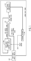
- Fig. 1 is a block diagram of an example logic chip 100, which includes a test mode input circuit 102 to receive an input indicating that activation of the test mode of the logic chip 100 is requested.
- the test mode input circuit 102 can include an input pin or multiple input pins, where the pin(s) can be coupled to an external pad (or pads). The external pad(s) can be set to a predefined value to indicate that test mode is requested.
- the input pin(s) of the test mode input circuit 102 can be coupled to the output of a controller or other device, where the controller or other device can set the input pin(s) to the predefined value to request entry of the logic chip 100 into the test mode.
- test mode input circuit 102 When the input pin(s) of the test mode input circuit 102 is (are) set to the predefined value indicating that test mode is requested, then the test mode input circuit 102 activates a test mode input signal 104, where the activation of the test mode input signal 104 is an indication that test mode is requested.
- Activation of a signal can refer to setting the signal to an active state (which can be a logic high or logic low state).
- Deactivation of a signal can refer to setting the signal to an inactive state (which can be a logic low or logic high state).
- the test mode input signal 104 is set to the active state (i.e. activated).
- the test mode input signal 104 is set to the inactive state (i.e. deactivated).
- the logic chip 100 also includes a test mode transition control circuit 106, which outputs a test mode enabling signal 108.
- the test mode transition control circuit 106 deactivates the test mode enabling signal 108 to prevent the logic chip 100 from transitioning from the functional mode to the test mode.
- a specified condition e.g.
- the test mode transition control circuit 106 activates the test mode enabling signal 108 to allow the logic chip 100 to transition from the functional mode to the test mode, in response to a request received at the test mode input circuit 102 to transition the logic chip 100 to the test mode.
- test mode enabling signal 108 is provided to a first input of an AND logic gate 110, while the test mode input signal 104 is provided to another input of the logic AND gate 110.
- the logic AND gate 110 is to activate a test mode signal 112 if both its inputs are in an active state. If either or both of the inputs to the logic AND gate 110 is (are) inactive, then the logic AND gate 110 deactivates the test mode signal 112.
- the test mode signal 112 when in the active state specifies that the logic chip 100 is in the test mode.
- the test mode signal 112 when in the inactive state specifies that the logic chip 100 is in the functional mode.
- the gate 110 can be a logic combination gate (including a combination of logic circuitry) that activates the test mode signal 112 only when both the test mode enabling signal 108 and the test mode input signal 104 are active.
- test mode transition control circuit 106 deactivates the test mode enabling signal 108
- the test mode signal 112 remains deactivated even if the test mode input signal 104 is activated by the test mode input circuit 102.
- the test mode enabling signal 108 when inactive causes the logic chip 100 to ignore the test mode input signal 104.
- the test mode signal 112 is provided as an input to a test mode controller 114.
- the test mode controller 114 can be a hardware processing circuit, or a combination of the hardware processing circuit and machine-readable instructions (software or firmware) executable on the hardware processing circuit.
- a hardware processing circuit can include a microprocessor, a core of a multi-core microprocessor, a microcontroller, a programmable gate array, a programmable integrated circuit, and so forth.
- the test mode controller 114 When the test mode signal 112 is activated, the test mode controller 114 is able to perform test operations to test respective features of the logic chip 100.
- the test operations can include accessing information stored in a storage element 116 in the logic chip 100.
- the storage element 116 can include a register.
- other types of storage elements can be included in the logic chip 100, where such other storage elements can also be accessed by the test mode controller 114 during a test operation in the test mode.
- the storage element 116 can be used to store sensitive information during operation of the logic chip 100 in the functional mode.
- the test mode transition control circuit 106 while the logic chip 100 is in the functional mode, the test mode transition control circuit 106 maintains the test mode enabling signal 108 in an inactive state, to prevent activation of the test mode signal 112 even if the test mode input circuit 102 asserts the test mode input signal 104 to an active state. This effectively prevents the logic chip 100 from transitioning from the functional mode to the test mode. Thus, even if a hacker were to set the input pin(s) of the test mode input circuit 102 to the predefined value for requesting that the logic chip 100 enter the test mode, the test mode transition control circuit 106 would prevent the logic chip 100 from transitioning to the test mode, which would prevent the hacker from accessing sensitive information that may be stored in the storage element 116.
- the logic chip 100 has to be first reset (or another condition has to occur that indicates that sensitive information has been rendered inaccessible, such as by clearing the sensitive information).
- a reset of the logic chip 100 is caused by activation of the reset signal 118.
- the reset signal 118 is provided as input to both the test mode transition control circuit 106 and the storage element 116.
- the reset signal 118 clears the storage element 116, such that any information (which can include sensitive information) stored in the storage element 116 is deleted, and thus, rendered inaccessible.
- the reset signal 118 when activated also causes the test mode transition control circuit 106 to activate the test mode enabling signal 108.
- Activating the test mode enabling signal 108 allows the logic AND gate 110 to activate the test mode signal 104 in response to activation of the test mode input signal 104.
- Activating the test mode signal 104 causes transition of the logic chip 100 from the functional mode to the test mode.
- the input pin(s) of the test mode input circuit 102 can be set to a value that indicates that the logic chip 100 is not to be placed in the test mode.
- the test mode input circuit 102 deactivates the test mode input signal 104, which causes deactivation of the test mode signal 112 by the logic AND gate 110 to place the logic chip 100 in the functional mode.
- Fig. 2 is a block diagram of the test mode transition control circuit 106 according to some examples of the present disclosure.
- the test mode transition control circuit 106 includes a disable circuit 202 that has a clock input 204 and a reset input 205.
- the disable circuit 202 outputs the test mode enabling signal 108.
- the clock input 104 of the disable circuit 202 is to receive a clock signal, which in Fig. 2 is a clock signal 208 that is passed through a clock gate 206.
- the clock gate 206 passes the clock signal 208 to the clock input 204 of the disable circuit 202 in response to the logic chip 100 being in the functional mode.
- the clock input 204 of the disable circuit 202 receives an active clock signal 208 and reset signal 118 is inactive, then the disable circuit 202 is able to perform its specified functionality of deactivating the test mode enabling signal 108.
- the disable circuit 202 in response to a first active edge (low-to-high transition or high-to-low transition depending on whether the clock signal 208 is active high or active low, respectively) of the clock signal 208, the disable circuit 202 is triggered to deactivate the test mode enabling signal 108. Once deactivation of the test mode enabling signal 108 is triggered by the first active edge of the clock signal 208, the disable circuit 202 is able to maintain the test mode enabling signal 108 deactivated, until the reset signal 118 is activated, as discussed further below.
- the clock gate 206 In response to the logic chip 100 being in the test mode, the clock gate 206 disables passing the clock signal 208 to the clock input 204 of the disable circuit 202. Instead, the clock gate 206 deactivates the clock input 204 of the disable circuit 202. If the clock input 204 of the disable circuit 202 is inactive (which means that the logic chip 100 has entered the test mode), then the disable circuit 202 is unable to change state and instead maintains the test mode enabling signal 108 at its previous state (which would be the active state once the logic chip 100 has entered the test mode). In other words, the disable circuit 202 maintains the test mode enabling signal 108 active while the logic chip 100 is in the test mode.
- the logic chip 100 Before the logic chip 100 can enter the test mode from the functional mode, the logic chip 100 has to satisfy a specified condition where sensitive information in the storage element 116 is rendered inaccessible, such as due to a reset. As further shown in Fig. 2 , the reset input 205 of the disable circuit 202 receives the reset signal 118. In response to activation of the reset signal 118, the disable circuit 202 is reset, which causes the disable circuit 202 to activate the test mode enabling signal 108, to enable the transition of the logic chip 100 from the functional mode to the test mode.
- Fig. 3 is a block diagram of further details associated with the test mode input circuit 102 and the test mode transition control circuit 106, according to further examples of the present disclosure.
- the test mode input circuit 102 includes multiple input pins 302 and a combination logic 304, which can include a combination of logic gates configured to receive a value provided to the input pins 302. In response to a specified value provided to the input pins 302, the combination logic 304 asserts the test mode input signal 104 to an active state.
- the test mode input circuit 102 can include just one input pin that is set to a value to indicate that the logic chip 100 is to enter the test mode.
- the test mode transition control circuit 106 includes a D flip-flop 306, which is a latch that has a data input (D) and a data output (Q).
- the D flip-flop 306 is an example of the disable circuit 202 of Fig. 2 . In other examples, the disable circuit 202 can be implemented with different logic.
- the D input of the D flip-flop 306 receives a binary "0" value (which is an example of an inactive value).
- the clock input 308 of the D flip-flop 306 receives an active clock signal
- the D flip-flop 306 drives the Q output to the value received at the D input, which in this case is the binary "0" value.
- the Q output of the D flip-flop 306 is driven to the value at the D input with each cycle of the input clock signal received at the clock input 308. Note that once the Q output of the D flip-flop 306 has been set to the binary "0" value of the D input in response to an active clock signal, the D flip-flop 306 maintains the binary "0" value at the Q output, even if no further clock edges of the clock signal are received (in other words, the clock signal is deactivated).
- the clock input 308 of the D flip-flop 306 is connected to the output of a clock gate 310, which is an example of the clock gate 206 in Fig. 2 .
- the clock gate 310 has an input to receive the clock signal 208, and an enable input (EN) connected to an enable signal output from an inverter 312.
- the input of the inverter 312 is connected to the output of the logic AND gate 110, or more specifically, to the test mode signal 112.
- the enable signal provided to the EN input of the clock gate 310 is active, which allows the clock signal 208 to pass through the clock gate 310 to the clock input 308 of the D flip-flop 306, and which causes the D flip-flop 306 to set the Q output to the value received at the D input.
- the D flip-flop 306 drives its Q output (and thus the test mode enabling signal 108) to an inactive state in response to an active edge of the clock signal 208, the D flip-flop maintains the Q output at the inactive state until a reset occurs.
- the D flip-flop 306 also has a reset input 309 to receive the reset signal 118. Activation of the reset signal 118 causes the D flip-flop 306 to be reset to binary "1" value, for example, which causes the test mode enabling signal 108 to be activated to the active state. As a result, the logic AND gate 110 is allowed to activate the test mode signal 112 in response to the test mode input signal 104 being set to the active state by the test mode input circuit 102.
- Fig. 4A is a flow diagram of an example process that can be performed in a logic chip, such as the logic chip 100 of Fig. 1 , to control a transition between a functional mode and a test mode of the logic chip.
- the process of Fig. 4A can be performed by the test mode transition control circuit 106 of Fig. 1 , for example.
- An example of the test mode transition control circuit 106 is depicted in Fig. 2 .
- the test mode transition control circuit 106 can have a different implementation, such as an implementation that includes a combination of a hardware processing circuit and machine-readable instructions executable on the hardware processing circuit.
- the process of Fig. 4A includes enabling (at 402) a clock input to a disable circuit (e.g. the disable circuit 202 in Fig. 2 ) in response to an indication that the logic chip is in the functional mode (e.g. the test mode signal 112 of Fig. 1 is in an inactive state).
- a disable circuit e.g. the disable circuit 202 in Fig. 2
- the process of Fig. 4A prevents (at 404) a transition from the functional mode of the logic chip to the test mode of the logic chip.
- the transition of the logic chip from the functional mode to the test mode is prevented by deactivating a test mode enabling signal (e.g. 108 in Fig. 1 , 2 , or 3 ).
- Deactivation of the test mode enabling signal is triggered in response to an first active edge of a clock signal (e.g. 208 in Fig. 2 or 3 ) that is provided to the clock input of the disable circuit.
- a clock signal e.g. 208 in Fig. 2 or 3
- the disable circuit 202 is able to maintain the test mode enabling signal 108 deactivated, until a reset or other condition that renders information in a storage element inaccessible occurs.
- the process of Fig. 4A disables (at 406) the clock input of the disable circuit in response to an indication that the logic chip is in the test mode (e.g. the test mode signal 112 of Fig. 1 is in an active state).
- the process of Fig. 4A enables (at 408) the transition of the logic chip from the functional mode to the test mode.
- Fig. 4B is a flow diagram of another example process that can be performed in a logic chip, such as the logic chip 100 of Fig. 1 , to control a transition between a functional mode and a test mode of the logic chip, according to further implementations.
- the process of Fig. 4B enables (at 422) a clock input to a disable circuit (e.g. the disable circuit 202 in Fig. 2 ) in response to an indication that the logic chip is in the functional mode.
- a test mode enabling signal e.g. 108 in Fig. 1 , 2 , or 3 ).
- the process of Fig. 4B receives (at 426) a request to transition to a test mode, such as in response to the input pins 302 being set to a predefined value.
- the process of Fig. 4B prevents (at 428) the requested transition from the functional mode to the test mode due to the test mode enabling signal being deactivated.
- the process of Fig. 4B enables (at 430) the transition of the logic chip from the functional mode to the test mode.
- the machine-readable instructions can be stored in a non-transitory machine-readable or computer-readable storage medium, which can include one or multiple different forms of memory including semiconductor memory devices such as dynamic or static random access memories (DRAMs or SRAMs), erasable and programmable read-only memories (EPROMs), electrically erasable and programmable read-only memories (EEPROMs) and flash memories; magnetic disks such as fixed, floppy and removable disks; other magnetic media including tape; optical media such as compact disks (CDs) or digital video disks (DVDs); or other types of storage devices.
- semiconductor memory devices such as dynamic or static random access memories (DRAMs or SRAMs), erasable and programmable read-only memories (EPROMs), electrically erasable and programmable read-only memories (EEPROMs) and flash memories
- magnetic disks such as fixed, floppy and removable disks
- optical media such as compact disks (CDs) or digital video disks (DVDs); or other
- the instructions discussed above can be provided on one computer-readable or machine-readable storage medium, or alternatively, can be provided on multiple computer-readable or machine-readable storage media distributed in a large system having possibly plural nodes.
- Such computer-readable or machine-readable storage medium or media is (are) considered to be part of an article (or article of manufacture).
- An article or article of manufacture can refer to any manufactured single component or multiple components.
- the storage medium or media can be located either in the machine running the machine-readable instructions, or located at a remote site from which machine-readable instructions can be downloaded over a network for execution.
Landscapes
- Engineering & Computer Science (AREA)
- General Engineering & Computer Science (AREA)
- Physics & Mathematics (AREA)
- General Physics & Mathematics (AREA)
- Semiconductor Integrated Circuits (AREA)
- Tests Of Electronic Circuits (AREA)
- Storage Device Security (AREA)
- Test And Diagnosis Of Digital Computers (AREA)
- For Increasing The Reliability Of Semiconductor Memories (AREA)
Description
- A logic chip can include various circuitry to provide respective functionalities. Examples of logic chips include integrated circuit (IC) chips. A logic chip can be operated in a test mode, which can be used to test functionalities of different parts of the logic chip.
US 2009/172819 A1 relates to a method and apparatus for implementing a logic security feature.US 2002/162065 A1 relates to a scan test circuit. - Some implementations of the present disclosure are described with respect to the following figures.
-
Fig. 1 is a block diagram of a logic chip including a test mode transition control circuit according to some examples. -
Fig. 2 is a block diagram of a test mode transition control circuit according to some examples. -
Fig. 3 is a block diagram of components of a test mode input circuit and a test mode transition control circuit, according to further examples. -
Figs. 4A and4B are flow diagrams of processes of controlling a transition between a functional mode and a test mode of a logic chip, according to some examples. - A logic chip can refer to any arrangement of circuitry that can be provided on a substrate, such as a semiconductor die, a circuit board, or any other support structure on which circuitry can be formed. The circuitry that can be included in a logic chip can include transistors, storage elements, and various other electronic elements that can be interconnected to provide respective functionalities. The logic chip also includes communication lines to interconnect the elements, where the communication lines can be implemented using electrically conductive traces or optical links.
- Examples of logic chips can include integrated circuit (IC) chips such as a microprocessor, a microcontroller, a memory device, a programmable gate array, a programmable integrated circuit, or any other type of electronic device.
- A logic chip can be provided with a test mode, sometimes referred to as a design for testability (DFT) mode. When the logic chip is placed into the test mode, various test operations can be run with respect to the logic chip, to test various features of the logic chip. In some examples, during test mode, storage elements (such as registers or other types of storage elements) can be accessed as part of test operations.
- In some examples, the storage elements that are accessed during the test mode can be designated for storing sensitive information during a functional mode of the logic chip. The functional mode of the logic chip is a mode of the logic chip during normal use of the logic chip, such as when the logic chip is incorporated into a larger system such as a computer, a smart phone, a game appliance, a vehicle, a wearable device (e.g. smart watch, smart eyeglasses, etc.), and so forth. The functional mode can also be referred to as a non-test mode.
- During the functional mode of the logic chip, sensitive information can be stored into one or multiple storage elements, such as a register. Sensitive information stored in a storage element can refer to any information that is intended to only be accessed by authorized entities, such as any or some combination of the following: authorized firmware, software, or other machine-readable instructions, authorized hardware devices, or authorized users. Examples of sensitive information can include cryptographic information (such as a key that is used to perform encryption and/or decryption of data), where the cryptographic information can be used to protect other data from unauthorized access. Other examples of sensitive information can include information that is confidential or proprietary to a particular enterprise or user.
- The test mode can be used by a manufacturer of the logic chip to confirm proper operation of the logic chip during the manufacture stage of the logic chip. In other examples, the test mode of the logic chip can be invoked at other times, such as when repair or debugging is desired. After testing is performed, the logic chip can be transitioned from the test mode to the functional mode.
- The presence of the test mode in a logic chip can present a potential security hole that can be exploited by a hacker to gain access to sensitive information stored in a storage element in the logic chip. The sensitive information is stored in the storage element during the functional mode of the logic chip. After the logic chip has been placed into the functional mode and after some sensitive information has been stored into the storage elements of the logic chip, a hacker can switch the logic chip to the test mode, to gain access to the sensitive information in the storage element.
- In accordance with some implementations of the present disclosure, a test mode transition control circuit is provided to control the transition between a functional mode of a logic chip and a test mode of the logic chip, to prevent unauthorized access of sensitive information stored in a storage element in the logic chip. The test mode transition control circuit restricts the transition from the functional mode to the test mode until a specific condition is satisfied (e.g. the
logic chip 100 is reset or some other condition that indicates that sensitive information stored in thelogic chip 100 has been rendered inaccessible). -
Fig. 1 is a block diagram of anexample logic chip 100, which includes a testmode input circuit 102 to receive an input indicating that activation of the test mode of thelogic chip 100 is requested. In some examples, the testmode input circuit 102 can include an input pin or multiple input pins, where the pin(s) can be coupled to an external pad (or pads). The external pad(s) can be set to a predefined value to indicate that test mode is requested. In other examples, the input pin(s) of the testmode input circuit 102 can be coupled to the output of a controller or other device, where the controller or other device can set the input pin(s) to the predefined value to request entry of thelogic chip 100 into the test mode. - When the input pin(s) of the test
mode input circuit 102 is (are) set to the predefined value indicating that test mode is requested, then the testmode input circuit 102 activates a testmode input signal 104, where the activation of the testmode input signal 104 is an indication that test mode is requested. Activation of a signal can refer to setting the signal to an active state (which can be a logic high or logic low state). Deactivation of a signal can refer to setting the signal to an inactive state (which can be a logic low or logic high state). If the input pin(s) of the testmode input circuit 102 is (are) set to the predefined value, then the testmode input signal 104 is set to the active state (i.e. activated). On the other hand, if the input pin(s) of the test mode input circuit is (are) not set to the predefined value, then the testmode input signal 104 is set to the inactive state (i.e. deactivated). - In accordance with some implementations of the present disclosure, the
logic chip 100 also includes a test modetransition control circuit 106, which outputs a testmode enabling signal 108. Generally, while thelogic chip 100 is in the functional mode, the test modetransition control circuit 106 deactivates the testmode enabling signal 108 to prevent thelogic chip 100 from transitioning from the functional mode to the test mode. However, when a specified condition occurs (e.g. thelogic chip 100 is reset by activation of areset signal 118, or some other condition occurs that indicates that sensitive information in thelogic chip 100 has been rendered inaccessible), the test modetransition control circuit 106 activates the testmode enabling signal 108 to allow thelogic chip 100 to transition from the functional mode to the test mode, in response to a request received at the testmode input circuit 102 to transition thelogic chip 100 to the test mode. - In some examples, the test
mode enabling signal 108 is provided to a first input of anAND logic gate 110, while the testmode input signal 104 is provided to another input of the logic ANDgate 110. The logic ANDgate 110 is to activate atest mode signal 112 if both its inputs are in an active state. If either or both of the inputs to the logic ANDgate 110 is (are) inactive, then the logic ANDgate 110 deactivates thetest mode signal 112. - The
test mode signal 112 when in the active state specifies that thelogic chip 100 is in the test mode. On the other hand, thetest mode signal 112 when in the inactive state specifies that thelogic chip 100 is in the functional mode. - In other examples, instead of being a logic AND gate, the
gate 110 can be a logic combination gate (including a combination of logic circuitry) that activates thetest mode signal 112 only when both the testmode enabling signal 108 and the testmode input signal 104 are active. - Effectively, when the test mode
transition control circuit 106 deactivates the testmode enabling signal 108, thetest mode signal 112 remains deactivated even if the testmode input signal 104 is activated by the testmode input circuit 102. The testmode enabling signal 108 when inactive causes thelogic chip 100 to ignore the testmode input signal 104. - The
test mode signal 112 is provided as an input to atest mode controller 114. Thetest mode controller 114 can be a hardware processing circuit, or a combination of the hardware processing circuit and machine-readable instructions (software or firmware) executable on the hardware processing circuit. A hardware processing circuit can include a microprocessor, a core of a multi-core microprocessor, a microcontroller, a programmable gate array, a programmable integrated circuit, and so forth. - When the
test mode signal 112 is activated, thetest mode controller 114 is able to perform test operations to test respective features of thelogic chip 100. The test operations can include accessing information stored in astorage element 116 in thelogic chip 100. In some examples, thestorage element 116 can include a register. In other examples, other types of storage elements can be included in thelogic chip 100, where such other storage elements can also be accessed by thetest mode controller 114 during a test operation in the test mode. Thestorage element 116 can be used to store sensitive information during operation of thelogic chip 100 in the functional mode. - In accordance with some implementations of the present disclosure, while the
logic chip 100 is in the functional mode, the test modetransition control circuit 106 maintains the testmode enabling signal 108 in an inactive state, to prevent activation of thetest mode signal 112 even if the testmode input circuit 102 asserts the testmode input signal 104 to an active state. This effectively prevents thelogic chip 100 from transitioning from the functional mode to the test mode. Thus, even if a hacker were to set the input pin(s) of the testmode input circuit 102 to the predefined value for requesting that thelogic chip 100 enter the test mode, the test modetransition control circuit 106 would prevent thelogic chip 100 from transitioning to the test mode, which would prevent the hacker from accessing sensitive information that may be stored in thestorage element 116. - To allow the
logic chip 100 to transition to the test mode, thelogic chip 100 has to be first reset (or another condition has to occur that indicates that sensitive information has been rendered inaccessible, such as by clearing the sensitive information). A reset of thelogic chip 100 is caused by activation of thereset signal 118. Thereset signal 118 is provided as input to both the test modetransition control circuit 106 and thestorage element 116. Thereset signal 118 clears thestorage element 116, such that any information (which can include sensitive information) stored in thestorage element 116 is deleted, and thus, rendered inaccessible. - The
reset signal 118 when activated also causes the test modetransition control circuit 106 to activate the testmode enabling signal 108. Activating the testmode enabling signal 108 allows the logic ANDgate 110 to activate thetest mode signal 104 in response to activation of the testmode input signal 104. Activating thetest mode signal 104 causes transition of thelogic chip 100 from the functional mode to the test mode. - To transition the
logic chip 100 from the test mode to the functional mode, the input pin(s) of the testmode input circuit 102 can be set to a value that indicates that thelogic chip 100 is not to be placed in the test mode. As a result, the testmode input circuit 102 deactivates the testmode input signal 104, which causes deactivation of thetest mode signal 112 by the logic ANDgate 110 to place thelogic chip 100 in the functional mode. -
Fig. 2 is a block diagram of the test modetransition control circuit 106 according to some examples of the present disclosure. The test modetransition control circuit 106 includes a disablecircuit 202 that has aclock input 204 and areset input 205. The disablecircuit 202 outputs the testmode enabling signal 108. - The
clock input 104 of the disablecircuit 202 is to receive a clock signal, which inFig. 2 is aclock signal 208 that is passed through aclock gate 206. Theclock gate 206 passes theclock signal 208 to theclock input 204 of the disablecircuit 202 in response to thelogic chip 100 being in the functional mode. When theclock input 204 of the disablecircuit 202 receives anactive clock signal 208 and resetsignal 118 is inactive, then the disablecircuit 202 is able to perform its specified functionality of deactivating the testmode enabling signal 108. In some examples, in response to a first active edge (low-to-high transition or high-to-low transition depending on whether theclock signal 208 is active high or active low, respectively) of theclock signal 208, the disablecircuit 202 is triggered to deactivate the testmode enabling signal 108. Once deactivation of the testmode enabling signal 108 is triggered by the first active edge of theclock signal 208, the disablecircuit 202 is able to maintain the testmode enabling signal 108 deactivated, until thereset signal 118 is activated, as discussed further below. - In response to the
logic chip 100 being in the test mode, theclock gate 206 disables passing theclock signal 208 to theclock input 204 of the disablecircuit 202. Instead, theclock gate 206 deactivates theclock input 204 of the disablecircuit 202. If theclock input 204 of the disablecircuit 202 is inactive (which means that thelogic chip 100 has entered the test mode), then the disablecircuit 202 is unable to change state and instead maintains the testmode enabling signal 108 at its previous state (which would be the active state once thelogic chip 100 has entered the test mode). In other words, the disablecircuit 202 maintains the testmode enabling signal 108 active while thelogic chip 100 is in the test mode. - Before the
logic chip 100 can enter the test mode from the functional mode, thelogic chip 100 has to satisfy a specified condition where sensitive information in thestorage element 116 is rendered inaccessible, such as due to a reset. As further shown inFig. 2 , thereset input 205 of the disablecircuit 202 receives thereset signal 118. In response to activation of thereset signal 118, the disablecircuit 202 is reset, which causes the disablecircuit 202 to activate the testmode enabling signal 108, to enable the transition of thelogic chip 100 from the functional mode to the test mode. -
Fig. 3 is a block diagram of further details associated with the testmode input circuit 102 and the test modetransition control circuit 106, according to further examples of the present disclosure. The testmode input circuit 102 includes multiple input pins 302 and acombination logic 304, which can include a combination of logic gates configured to receive a value provided to the input pins 302. In response to a specified value provided to the input pins 302, thecombination logic 304 asserts the testmode input signal 104 to an active state. In other examples, instead of multiple input pins 302, the testmode input circuit 102 can include just one input pin that is set to a value to indicate that thelogic chip 100 is to enter the test mode. - The test mode
transition control circuit 106 includes a D flip-flop 306, which is a latch that has a data input (D) and a data output (Q). The D flip-flop 306 is an example of the disablecircuit 202 ofFig. 2 . In other examples, the disablecircuit 202 can be implemented with different logic. In the example ofFig. 3 , the D input of the D flip-flop 306 receives a binary "0" value (which is an example of an inactive value). When theclock input 308 of the D flip-flop 306 receives an active clock signal, the D flip-flop 306 drives the Q output to the value received at the D input, which in this case is the binary "0" value. The Q output of the D flip-flop 306 is driven to the value at the D input with each cycle of the input clock signal received at theclock input 308. Note that once the Q output of the D flip-flop 306 has been set to the binary "0" value of the D input in response to an active clock signal, the D flip-flop 306 maintains the binary "0" value at the Q output, even if no further clock edges of the clock signal are received (in other words, the clock signal is deactivated). - The
clock input 308 of the D flip-flop 306 is connected to the output of aclock gate 310, which is an example of theclock gate 206 inFig. 2 . Theclock gate 310 has an input to receive theclock signal 208, and an enable input (EN) connected to an enable signal output from aninverter 312. The input of theinverter 312 is connected to the output of the logic ANDgate 110, or more specifically, to thetest mode signal 112. When thetest mode signal 112 is in an inactive state, which indicates that thelogic chip 100 is in the functional mode, then the enable signal provided to the EN input of theclock gate 310 is active, which allows theclock signal 208 to pass through theclock gate 310 to theclock input 308 of the D flip-flop 306, and which causes the D flip-flop 306 to set the Q output to the value received at the D input. This causes the testmode enabling signal 108 to be deactivated to the inactive state, which prevents activation of thetest mode signal 112 and thus prevents a transition of thelogic chip 100 to the test mode. Once the D flip-flop 306 drives its Q output (and thus the test mode enabling signal 108) to an inactive state in response to an active edge of theclock signal 208, the D flip-flop maintains the Q output at the inactive state until a reset occurs. - The D flip-
flop 306 also has areset input 309 to receive thereset signal 118. Activation of thereset signal 118 causes the D flip-flop 306 to be reset to binary "1" value, for example, which causes the testmode enabling signal 108 to be activated to the active state. As a result, the logic ANDgate 110 is allowed to activate thetest mode signal 112 in response to the testmode input signal 104 being set to the active state by the testmode input circuit 102. -
Fig. 4A is a flow diagram of an example process that can be performed in a logic chip, such as thelogic chip 100 ofFig. 1 , to control a transition between a functional mode and a test mode of the logic chip. The process ofFig. 4A can be performed by the test modetransition control circuit 106 ofFig. 1 , for example. An example of the test modetransition control circuit 106 is depicted inFig. 2 . In other examples, the test modetransition control circuit 106 can have a different implementation, such as an implementation that includes a combination of a hardware processing circuit and machine-readable instructions executable on the hardware processing circuit. - The process of
Fig. 4A includes enabling (at 402) a clock input to a disable circuit (e.g. the disablecircuit 202 inFig. 2 ) in response to an indication that the logic chip is in the functional mode (e.g. thetest mode signal 112 ofFig. 1 is in an inactive state). In response to the clock input to the disable circuit being enabled, the process ofFig. 4A prevents (at 404) a transition from the functional mode of the logic chip to the test mode of the logic chip. In some examples, as discussed above, the transition of the logic chip from the functional mode to the test mode is prevented by deactivating a test mode enabling signal (e.g. 108 inFig. 1 ,2 , or3 ). Deactivation of the test mode enabling signal is triggered in response to an first active edge of a clock signal (e.g. 208 inFig. 2 or3 ) that is provided to the clock input of the disable circuit. Once deactivation of the testmode enabling signal 108 is triggered by the first active edge of theclock signal 208, the disablecircuit 202 is able to maintain the testmode enabling signal 108 deactivated, until a reset or other condition that renders information in a storage element inaccessible occurs. - The process of
Fig. 4A disables (at 406) the clock input of the disable circuit in response to an indication that the logic chip is in the test mode (e.g. thetest mode signal 112 ofFig. 1 is in an active state). In response to detecting a condition of the logic chip that renders information in a storage element inaccessible (such as when thereset signal 118 is activated), the process ofFig. 4A enables (at 408) the transition of the logic chip from the functional mode to the test mode. -
Fig. 4B is a flow diagram of another example process that can be performed in a logic chip, such as thelogic chip 100 ofFig. 1 , to control a transition between a functional mode and a test mode of the logic chip, according to further implementations. The process ofFig. 4B enables (at 422) a clock input to a disable circuit (e.g. the disablecircuit 202 inFig. 2 ) in response to an indication that the logic chip is in the functional mode. Once the clock input is enabled and a clock edge occurs, the process ofFig. 4B deactivates (at 424) a test mode enabling signal (e.g. 108 inFig. 1 ,2 , or3 ). - The process of
Fig. 4B receives (at 426) a request to transition to a test mode, such as in response to the input pins 302 being set to a predefined value. The process ofFig. 4B prevents (at 428) the requested transition from the functional mode to the test mode due to the test mode enabling signal being deactivated. In response to detecting a condition of the logic chip that renders information in a storage element inaccessible (such as when thereset signal 118 is activated), the process ofFig. 4B enables (at 430) the transition of the logic chip from the functional mode to the test mode. - In examples where the test mode
transition control circuit 106 is implemented as a combination of a hardware processing circuit and machine-readable instructions, the machine-readable instructions can be stored in a non-transitory machine-readable or computer-readable storage medium, which can include one or multiple different forms of memory including semiconductor memory devices such as dynamic or static random access memories (DRAMs or SRAMs), erasable and programmable read-only memories (EPROMs), electrically erasable and programmable read-only memories (EEPROMs) and flash memories; magnetic disks such as fixed, floppy and removable disks; other magnetic media including tape; optical media such as compact disks (CDs) or digital video disks (DVDs); or other types of storage devices. Note that the instructions discussed above can be provided on one computer-readable or machine-readable storage medium, or alternatively, can be provided on multiple computer-readable or machine-readable storage media distributed in a large system having possibly plural nodes. Such computer-readable or machine-readable storage medium or media is (are) considered to be part of an article (or article of manufacture). An article or article of manufacture can refer to any manufactured single component or multiple components. The storage medium or media can be located either in the machine running the machine-readable instructions, or located at a remote site from which machine-readable instructions can be downloaded over a network for execution. - In the foregoing description, numerous details are set forth to provide an understanding of the subject disclosed herein. The scope of the invention is defined by the appended claims.
Claims (15)
- A method of controlling a transition between a functional mode and a test mode of a logic chip, comprising:enabling (402) a clock input of a disable circuit in response to an indication that the logic chip is in the functional mode;in response to the clock input of the disable circuit being enabled, preventing (404) a transition from the functional mode of the logic chip to the test mode of the logic chip;disabling (406) the clock input of the disable circuit in response to an indication that the logic chip is in the test mode; and characterized byin response to detecting a condition of the logic chip that renders information in a storage element inaccessible, enabling (408) the transition of the logic chip from the functional mode to the test mode.
- The method of claim 1, wherein detecting the condition comprises receiving activation of a reset signal to reset the logic chip.
- The method of claim 2, further comprising resetting the disable circuit in response to the activation of the reset signal.
- The method of claim 3, wherein resetting the disable circuit causes the disable circuit to activate a first signal input to a logic gate that further receives a second signal that when activated indicates that the logic chip is to enter the test mode.
- The method of claim 4, further comprising:
in response to an active edge of the clock input to the disable circuit, setting the first signal to an inactive state. - The method of claim 5, further comprising:
while the clock input to the disable circuit is disabled, maintaining the first signal at a previous state. - The method of claim 4, further comprising:
activating, by the logic gate, a test mode signal in response to both the first and second signals being active, wherein the activated test mode signal is an indication of the logic chip being in the test mode. - The method of claim 7, further comprising:
performing, by a test mode controller, a test operation in response to the activating of the test mode signal, the test mode operation comprising accessing a content in the storage element. - The method of claim 4, further comprising:
activating the second signal in response to at least one input pin of the logic chip being set to a predefined value. - A test mode transition control circuit (106) for a logic chip (100), comprising:a disable circuit (202) comprising a clock input;a clock gate (206) to:enable passing a clock signal (208) to the clock input (204) of the disable circuit in response to the logic chip being in a functional mode, anddisable passing the clock signal to the clock input of the disable circuit in response to the logic chip being in a test mode; characterized in thatthe disable circuit to deactivate a test mode enabling signal (108) in response to the clock input of the disable circuit receiving the clock signal through the clock gate, wherein the deactivated test mode enabling signal prevents a transition of the logic chip from the functional mode to the test mode, andthe disable circuit to activate the test mode enabling signal in response to a reset of the logic chip.
- The test mode transition control circuit (106) of claim 10, wherein the disable circuit (202) comprises a D flip-flop (306) that has an input set to an inactive value, wherein an output of the D flip-flop is driven to the inactive value responsible to each cycle of the clock signal (208).
- The test mode transition control circuit (106) of claim 10, wherein the disable circuit (202) is to maintain the test mode enabling signal (108) active while the logic chip (100) is in the test mode.
- The test mode transition control circuit (106) of claim 10, wherein the clock gate (206) comprises:an enable input to receive an enable signal that when in an active state indicates that the logic chip is in the functional mode, and when in an inactive state indicates that the logic chip is in the test mode, andan input to receive the clock signal, the clock gate to pass the clock signal through the clock gate responsive to the enable signal being in the active state.
- A logic chip (100) comprising:the test mode transition control circuit (106) of claim 10;a test mode input circuit (102) to activate a test mode input signal in response to an input to request that the logic chip be placed in a test mode;wherein the clock input is enabled in response to an indication that the logic chip is in a functional mode, and that is disabled in response to an indication that the logic chip is in the test mode, the disable circuit to, once the clock input of the disable circuit is enabled and a clock edge occurs, deactivate the test mode enabling signal to prevent a transition of the logic chip from the functional mode to the test mode, and the disable circuit to activate the test mode enabling signal in response to detecting a reset of the logic chip;a logic gate (110) to cause the logic chip to enter the test mode in response to the test mode input signal being activated and the test mode enabling signal being activated; anda test controller (114) to perform a test operation during the test mode.
- The logic chip (100) of claim 14, further comprising a storage element (116) to store sensitive information during the functional mode of the logic chip, wherein the reset renders the sensitive information in the storage element inaccessible.
Applications Claiming Priority (1)
| Application Number | Priority Date | Filing Date | Title |
|---|---|---|---|
| PCT/US2016/022640 WO2017160286A1 (en) | 2016-03-16 | 2016-03-16 | Controlling a transition between a functional mode and a test mode |
Publications (3)
| Publication Number | Publication Date |
|---|---|
| EP3430627A1 EP3430627A1 (en) | 2019-01-23 |
| EP3430627A4 EP3430627A4 (en) | 2019-10-23 |
| EP3430627B1 true EP3430627B1 (en) | 2022-01-12 |
Family
ID=59851858
Family Applications (1)
| Application Number | Title | Priority Date | Filing Date |
|---|---|---|---|
| EP16894745.5A Not-in-force EP3430627B1 (en) | 2016-03-16 | 2016-03-16 | Controlling a transition between a functional mode and a test mode |
Country Status (5)
| Country | Link |
|---|---|
| US (1) | US20180328988A1 (en) |
| EP (1) | EP3430627B1 (en) |
| JP (1) | JP6656398B2 (en) |
| CN (1) | CN108496222A (en) |
| WO (1) | WO2017160286A1 (en) |
Families Citing this family (7)
| Publication number | Priority date | Publication date | Assignee | Title |
|---|---|---|---|---|
| CN111856258B (en) * | 2020-07-24 | 2023-05-09 | 北京百度网讯科技有限公司 | Method, device, storage medium and corresponding chip for chip testing |
| CN112882402A (en) * | 2021-01-18 | 2021-06-01 | 湖南国科微电子股份有限公司 | Control method, device, equipment and medium of integrated chip |
| CN114415001B (en) * | 2021-12-15 | 2025-05-27 | 上海泰矽微电子有限公司 | Chip test mode switching method and system |
| CN114814531B (en) * | 2022-03-30 | 2024-04-30 | 上海先楫半导体科技有限公司 | Chip safety test circuit and logic chip |
| JP7847647B2 (en) * | 2022-05-30 | 2026-04-17 | 日清紡マイクロデバイス株式会社 | Electronic circuits and their testing methods |
| KR20240070151A (en) * | 2022-11-14 | 2024-05-21 | 에스케이하이닉스 주식회사 | Test mode control circuit, a semiconductor apparatus, and a semiconductor system including the same |
| CN120415600B (en) * | 2025-07-03 | 2025-09-05 | 上海亿晶微电子科技有限公司 | An automatic gain control test circuit for infrared receiving chip |
Family Cites Families (14)
| Publication number | Priority date | Publication date | Assignee | Title |
|---|---|---|---|---|
| JP4627118B2 (en) * | 2001-04-26 | 2011-02-09 | ルネサスエレクトロニクス株式会社 | Scan test circuit |
| US7185249B2 (en) * | 2002-04-30 | 2007-02-27 | Freescale Semiconductor, Inc. | Method and apparatus for secure scan testing |
| EP1439398A1 (en) * | 2003-01-16 | 2004-07-21 | STMicroelectronics Limited | Scan chain arrangement |
| US20050138500A1 (en) * | 2003-11-25 | 2005-06-23 | Chimsong Sul | Functional test design for testability (DFT) and test architecture for decreased tester channel resources |
| JP4213605B2 (en) * | 2004-02-26 | 2009-01-21 | 東芝エルエスアイシステムサポート株式会社 | Operation mode setting circuit |
| US7134106B2 (en) * | 2004-04-09 | 2006-11-07 | Incentia Design Systems Corp. | Method and system for providing fast design for testability prototyping in integrated circuit designs |
| US7992062B2 (en) * | 2006-06-22 | 2011-08-02 | Qualcomm Incorporated | Logic device and method supporting scan test |
| JP4953788B2 (en) * | 2006-12-05 | 2012-06-13 | 株式会社デンソー | Electronic equipment |
| US7941722B2 (en) * | 2007-06-24 | 2011-05-10 | Texas Instruments Incorporated | Testing of integrated circuits using test module |
| US8166357B2 (en) * | 2007-12-26 | 2012-04-24 | International Business Machines Corporation | Implementing logic security feature for disabling integrated circuit test ports ability to scanout data |
| US7962819B2 (en) * | 2008-01-24 | 2011-06-14 | Sandisk Corporation | Test mode soft reset circuitry and methods |
| US8051345B2 (en) * | 2008-06-04 | 2011-11-01 | Ati Technologies Ulc | Method and apparatus for securing digital information on an integrated circuit during test operating modes |
| JP5446358B2 (en) * | 2009-03-24 | 2014-03-19 | 富士通セミコンダクター株式会社 | Semiconductor integrated circuit and test method thereof |
| JP2014044073A (en) * | 2012-08-24 | 2014-03-13 | Renesas Electronics Corp | Semiconductor device and method of controlling semiconductor device |
-
2016
- 2016-03-16 JP JP2018545265A patent/JP6656398B2/en not_active Expired - Fee Related
- 2016-03-16 EP EP16894745.5A patent/EP3430627B1/en not_active Not-in-force
- 2016-03-16 WO PCT/US2016/022640 patent/WO2017160286A1/en not_active Ceased
- 2016-03-16 CN CN201680079099.6A patent/CN108496222A/en active Pending
- 2016-03-16 US US15/775,734 patent/US20180328988A1/en not_active Abandoned
Also Published As
| Publication number | Publication date |
|---|---|
| EP3430627A1 (en) | 2019-01-23 |
| US20180328988A1 (en) | 2018-11-15 |
| JP6656398B2 (en) | 2020-03-04 |
| CN108496222A (en) | 2018-09-04 |
| EP3430627A4 (en) | 2019-10-23 |
| WO2017160286A1 (en) | 2017-09-21 |
| JP2019514094A (en) | 2019-05-30 |
Similar Documents
| Publication | Publication Date | Title |
|---|---|---|
| EP3430627B1 (en) | Controlling a transition between a functional mode and a test mode | |
| US7185249B2 (en) | Method and apparatus for secure scan testing | |
| EP3287800B1 (en) | Jtag debug apparatus and jtag debug method | |
| US7117352B1 (en) | Debug port disable mechanism | |
| US10289840B2 (en) | Integrated circuit with tamper protection and method therefor | |
| US8051345B2 (en) | Method and apparatus for securing digital information on an integrated circuit during test operating modes | |
| US6968420B1 (en) | Use of EEPROM for storage of security objects in secure systems | |
| US20220027520A1 (en) | Methods And Apparatus For In-Memory Device Access Control | |
| US8621195B2 (en) | Disabling communication ports | |
| JP2006505022A (en) | Integrated circuit security and method | |
| US9696772B2 (en) | Controlling access to a memory | |
| US8438436B1 (en) | Secure design-for-test scan chains | |
| KR20100070027A (en) | Apparatus including function of authenticating joint test action group and the authenticating method | |
| US20220035956A1 (en) | Password-based access control for programmable logic devices | |
| US7228440B1 (en) | Scan and boundary scan disable mechanism on secure device | |
| US20190050570A1 (en) | Computer resource access control based on the state of a non-accessing component | |
| US9939074B2 (en) | Enabling secured debug of an integrated circuit | |
| US8397079B2 (en) | Method and apparatus for securing digital information on an integrated circuit read only memory during test operating modes | |
| US7254716B1 (en) | Security supervisor governing allowed transactions on a system bus | |
| US7254720B1 (en) | Precise exit logic for removal of security overlay of instruction space | |
| US9910794B2 (en) | Processing data | |
| US9792461B2 (en) | Control apparatus | |
| CN120145377A (en) | Method, device and equipment for detecting encrypted IP during operation of system on chip |
Legal Events
| Date | Code | Title | Description |
|---|---|---|---|
| STAA | Information on the status of an ep patent application or granted ep patent |
Free format text: STATUS: THE INTERNATIONAL PUBLICATION HAS BEEN MADE |
|
| PUAI | Public reference made under article 153(3) epc to a published international application that has entered the european phase |
Free format text: ORIGINAL CODE: 0009012 |
|
| STAA | Information on the status of an ep patent application or granted ep patent |
Free format text: STATUS: REQUEST FOR EXAMINATION WAS MADE |
|
| 17P | Request for examination filed |
Effective date: 20180723 |
|
| AK | Designated contracting states |
Kind code of ref document: A1 Designated state(s): AL AT BE BG CH CY CZ DE DK EE ES FI FR GB GR HR HU IE IS IT LI LT LU LV MC MK MT NL NO PL PT RO RS SE SI SK SM TR |
|
| AX | Request for extension of the european patent |
Extension state: BA ME |
|
| RAP1 | Party data changed (applicant data changed or rights of an application transferred) |
Owner name: HEWLETT-PACKARD DEVELOPMENT COMPANY, L.P. |
|
| DAV | Request for validation of the european patent (deleted) | ||
| DAX | Request for extension of the european patent (deleted) | ||
| A4 | Supplementary search report drawn up and despatched |
Effective date: 20190924 |
|
| RIC1 | Information provided on ipc code assigned before grant |
Ipc: G11C 29/04 20060101ALI20190918BHEP Ipc: G01R 31/3185 20060101ALI20190918BHEP Ipc: G11C 29/46 20060101ALI20190918BHEP Ipc: G11C 29/14 20060101ALI20190918BHEP Ipc: G11C 29/02 20060101AFI20190918BHEP Ipc: G01R 31/317 20060101ALI20190918BHEP |
|
| GRAP | Despatch of communication of intention to grant a patent |
Free format text: ORIGINAL CODE: EPIDOSNIGR1 |
|
| STAA | Information on the status of an ep patent application or granted ep patent |
Free format text: STATUS: GRANT OF PATENT IS INTENDED |
|
| INTG | Intention to grant announced |
Effective date: 20211028 |
|
| GRAS | Grant fee paid |
Free format text: ORIGINAL CODE: EPIDOSNIGR3 |
|
| GRAA | (expected) grant |
Free format text: ORIGINAL CODE: 0009210 |
|
| STAA | Information on the status of an ep patent application or granted ep patent |
Free format text: STATUS: THE PATENT HAS BEEN GRANTED |
|
| AK | Designated contracting states |
Kind code of ref document: B1 Designated state(s): AL AT BE BG CH CY CZ DE DK EE ES FI FR GB GR HR HU IE IS IT LI LT LU LV MC MK MT NL NO PL PT RO RS SE SI SK SM TR |
|
| REG | Reference to a national code |
Ref country code: GB Ref legal event code: FG4D |
|
| REG | Reference to a national code |
Ref country code: CH Ref legal event code: EP |
|
| REG | Reference to a national code |
Ref country code: DE Ref legal event code: R096 Ref document number: 602016068401 Country of ref document: DE |
|
| REG | Reference to a national code |
Ref country code: IE Ref legal event code: FG4D |
|
| REG | Reference to a national code |
Ref country code: AT Ref legal event code: REF Ref document number: 1462907 Country of ref document: AT Kind code of ref document: T Effective date: 20220215 |
|
| PGFP | Annual fee paid to national office [announced via postgrant information from national office to epo] |
Ref country code: GB Payment date: 20220315 Year of fee payment: 7 Ref country code: DE Payment date: 20220217 Year of fee payment: 7 |
|
| REG | Reference to a national code |
Ref country code: LT Ref legal event code: MG9D |
|
| REG | Reference to a national code |
Ref country code: NL Ref legal event code: MP Effective date: 20220112 |
|
| PGFP | Annual fee paid to national office [announced via postgrant information from national office to epo] |
Ref country code: FR Payment date: 20220218 Year of fee payment: 7 |
|
| REG | Reference to a national code |
Ref country code: AT Ref legal event code: MK05 Ref document number: 1462907 Country of ref document: AT Kind code of ref document: T Effective date: 20220112 |
|
| PG25 | Lapsed in a contracting state [announced via postgrant information from national office to epo] |
Ref country code: NL Free format text: LAPSE BECAUSE OF FAILURE TO SUBMIT A TRANSLATION OF THE DESCRIPTION OR TO PAY THE FEE WITHIN THE PRESCRIBED TIME-LIMIT Effective date: 20220112 |
|
| PG25 | Lapsed in a contracting state [announced via postgrant information from national office to epo] |
Ref country code: SE Free format text: LAPSE BECAUSE OF FAILURE TO SUBMIT A TRANSLATION OF THE DESCRIPTION OR TO PAY THE FEE WITHIN THE PRESCRIBED TIME-LIMIT Effective date: 20220112 Ref country code: RS Free format text: LAPSE BECAUSE OF FAILURE TO SUBMIT A TRANSLATION OF THE DESCRIPTION OR TO PAY THE FEE WITHIN THE PRESCRIBED TIME-LIMIT Effective date: 20220112 Ref country code: PT Free format text: LAPSE BECAUSE OF FAILURE TO SUBMIT A TRANSLATION OF THE DESCRIPTION OR TO PAY THE FEE WITHIN THE PRESCRIBED TIME-LIMIT Effective date: 20220512 Ref country code: NO Free format text: LAPSE BECAUSE OF FAILURE TO SUBMIT A TRANSLATION OF THE DESCRIPTION OR TO PAY THE FEE WITHIN THE PRESCRIBED TIME-LIMIT Effective date: 20220412 Ref country code: LT Free format text: LAPSE BECAUSE OF FAILURE TO SUBMIT A TRANSLATION OF THE DESCRIPTION OR TO PAY THE FEE WITHIN THE PRESCRIBED TIME-LIMIT Effective date: 20220112 Ref country code: HR Free format text: LAPSE BECAUSE OF FAILURE TO SUBMIT A TRANSLATION OF THE DESCRIPTION OR TO PAY THE FEE WITHIN THE PRESCRIBED TIME-LIMIT Effective date: 20220112 Ref country code: ES Free format text: LAPSE BECAUSE OF FAILURE TO SUBMIT A TRANSLATION OF THE DESCRIPTION OR TO PAY THE FEE WITHIN THE PRESCRIBED TIME-LIMIT Effective date: 20220112 Ref country code: BG Free format text: LAPSE BECAUSE OF FAILURE TO SUBMIT A TRANSLATION OF THE DESCRIPTION OR TO PAY THE FEE WITHIN THE PRESCRIBED TIME-LIMIT Effective date: 20220412 |
|
| PG25 | Lapsed in a contracting state [announced via postgrant information from national office to epo] |
Ref country code: PL Free format text: LAPSE BECAUSE OF FAILURE TO SUBMIT A TRANSLATION OF THE DESCRIPTION OR TO PAY THE FEE WITHIN THE PRESCRIBED TIME-LIMIT Effective date: 20220112 Ref country code: LV Free format text: LAPSE BECAUSE OF FAILURE TO SUBMIT A TRANSLATION OF THE DESCRIPTION OR TO PAY THE FEE WITHIN THE PRESCRIBED TIME-LIMIT Effective date: 20220112 Ref country code: GR Free format text: LAPSE BECAUSE OF FAILURE TO SUBMIT A TRANSLATION OF THE DESCRIPTION OR TO PAY THE FEE WITHIN THE PRESCRIBED TIME-LIMIT Effective date: 20220413 Ref country code: FI Free format text: LAPSE BECAUSE OF FAILURE TO SUBMIT A TRANSLATION OF THE DESCRIPTION OR TO PAY THE FEE WITHIN THE PRESCRIBED TIME-LIMIT Effective date: 20220112 Ref country code: AT Free format text: LAPSE BECAUSE OF FAILURE TO SUBMIT A TRANSLATION OF THE DESCRIPTION OR TO PAY THE FEE WITHIN THE PRESCRIBED TIME-LIMIT Effective date: 20220112 |
|
| PG25 | Lapsed in a contracting state [announced via postgrant information from national office to epo] |
Ref country code: IS Free format text: LAPSE BECAUSE OF FAILURE TO SUBMIT A TRANSLATION OF THE DESCRIPTION OR TO PAY THE FEE WITHIN THE PRESCRIBED TIME-LIMIT Effective date: 20220512 |
|
| REG | Reference to a national code |
Ref country code: DE Ref legal event code: R097 Ref document number: 602016068401 Country of ref document: DE |
|
| PG25 | Lapsed in a contracting state [announced via postgrant information from national office to epo] |
Ref country code: SM Free format text: LAPSE BECAUSE OF FAILURE TO SUBMIT A TRANSLATION OF THE DESCRIPTION OR TO PAY THE FEE WITHIN THE PRESCRIBED TIME-LIMIT Effective date: 20220112 Ref country code: SK Free format text: LAPSE BECAUSE OF FAILURE TO SUBMIT A TRANSLATION OF THE DESCRIPTION OR TO PAY THE FEE WITHIN THE PRESCRIBED TIME-LIMIT Effective date: 20220112 Ref country code: RO Free format text: LAPSE BECAUSE OF FAILURE TO SUBMIT A TRANSLATION OF THE DESCRIPTION OR TO PAY THE FEE WITHIN THE PRESCRIBED TIME-LIMIT Effective date: 20220112 Ref country code: MC Free format text: LAPSE BECAUSE OF FAILURE TO SUBMIT A TRANSLATION OF THE DESCRIPTION OR TO PAY THE FEE WITHIN THE PRESCRIBED TIME-LIMIT Effective date: 20220112 Ref country code: EE Free format text: LAPSE BECAUSE OF FAILURE TO SUBMIT A TRANSLATION OF THE DESCRIPTION OR TO PAY THE FEE WITHIN THE PRESCRIBED TIME-LIMIT Effective date: 20220112 Ref country code: DK Free format text: LAPSE BECAUSE OF FAILURE TO SUBMIT A TRANSLATION OF THE DESCRIPTION OR TO PAY THE FEE WITHIN THE PRESCRIBED TIME-LIMIT Effective date: 20220112 Ref country code: CZ Free format text: LAPSE BECAUSE OF FAILURE TO SUBMIT A TRANSLATION OF THE DESCRIPTION OR TO PAY THE FEE WITHIN THE PRESCRIBED TIME-LIMIT Effective date: 20220112 |
|
| REG | Reference to a national code |
Ref country code: CH Ref legal event code: PL |
|
| PLBE | No opposition filed within time limit |
Free format text: ORIGINAL CODE: 0009261 |
|
| STAA | Information on the status of an ep patent application or granted ep patent |
Free format text: STATUS: NO OPPOSITION FILED WITHIN TIME LIMIT |
|
| PG25 | Lapsed in a contracting state [announced via postgrant information from national office to epo] |
Ref country code: AL Free format text: LAPSE BECAUSE OF FAILURE TO SUBMIT A TRANSLATION OF THE DESCRIPTION OR TO PAY THE FEE WITHIN THE PRESCRIBED TIME-LIMIT Effective date: 20220112 |
|
| REG | Reference to a national code |
Ref country code: BE Ref legal event code: MM Effective date: 20220331 |
|
| 26N | No opposition filed |
Effective date: 20221013 |
|
| PG25 | Lapsed in a contracting state [announced via postgrant information from national office to epo] |
Ref country code: LU Free format text: LAPSE BECAUSE OF NON-PAYMENT OF DUE FEES Effective date: 20220316 Ref country code: LI Free format text: LAPSE BECAUSE OF NON-PAYMENT OF DUE FEES Effective date: 20220331 Ref country code: IE Free format text: LAPSE BECAUSE OF NON-PAYMENT OF DUE FEES Effective date: 20220316 Ref country code: CH Free format text: LAPSE BECAUSE OF NON-PAYMENT OF DUE FEES Effective date: 20220331 |
|
| PG25 | Lapsed in a contracting state [announced via postgrant information from national office to epo] |
Ref country code: SI Free format text: LAPSE BECAUSE OF FAILURE TO SUBMIT A TRANSLATION OF THE DESCRIPTION OR TO PAY THE FEE WITHIN THE PRESCRIBED TIME-LIMIT Effective date: 20220112 Ref country code: BE Free format text: LAPSE BECAUSE OF NON-PAYMENT OF DUE FEES Effective date: 20220331 |
|
| PG25 | Lapsed in a contracting state [announced via postgrant information from national office to epo] |
Ref country code: IT Free format text: LAPSE BECAUSE OF FAILURE TO SUBMIT A TRANSLATION OF THE DESCRIPTION OR TO PAY THE FEE WITHIN THE PRESCRIBED TIME-LIMIT Effective date: 20220112 |
|
| REG | Reference to a national code |
Ref country code: DE Ref legal event code: R119 Ref document number: 602016068401 Country of ref document: DE |
|
| GBPC | Gb: european patent ceased through non-payment of renewal fee |
Effective date: 20230316 |
|
| PG25 | Lapsed in a contracting state [announced via postgrant information from national office to epo] |
Ref country code: GB Free format text: LAPSE BECAUSE OF NON-PAYMENT OF DUE FEES Effective date: 20230316 |
|
| PG25 | Lapsed in a contracting state [announced via postgrant information from national office to epo] |
Ref country code: GB Free format text: LAPSE BECAUSE OF NON-PAYMENT OF DUE FEES Effective date: 20230316 Ref country code: FR Free format text: LAPSE BECAUSE OF NON-PAYMENT OF DUE FEES Effective date: 20230331 Ref country code: DE Free format text: LAPSE BECAUSE OF NON-PAYMENT OF DUE FEES Effective date: 20231003 |
|
| PG25 | Lapsed in a contracting state [announced via postgrant information from national office to epo] |
Ref country code: HU Free format text: LAPSE BECAUSE OF FAILURE TO SUBMIT A TRANSLATION OF THE DESCRIPTION OR TO PAY THE FEE WITHIN THE PRESCRIBED TIME-LIMIT; INVALID AB INITIO Effective date: 20160316 |
|
| PG25 | Lapsed in a contracting state [announced via postgrant information from national office to epo] |
Ref country code: MK Free format text: LAPSE BECAUSE OF FAILURE TO SUBMIT A TRANSLATION OF THE DESCRIPTION OR TO PAY THE FEE WITHIN THE PRESCRIBED TIME-LIMIT Effective date: 20220112 Ref country code: CY Free format text: LAPSE BECAUSE OF FAILURE TO SUBMIT A TRANSLATION OF THE DESCRIPTION OR TO PAY THE FEE WITHIN THE PRESCRIBED TIME-LIMIT Effective date: 20220112 |
|
| PG25 | Lapsed in a contracting state [announced via postgrant information from national office to epo] |
Ref country code: MT Free format text: LAPSE BECAUSE OF FAILURE TO SUBMIT A TRANSLATION OF THE DESCRIPTION OR TO PAY THE FEE WITHIN THE PRESCRIBED TIME-LIMIT Effective date: 20220112 |
|
| PG25 | Lapsed in a contracting state [announced via postgrant information from national office to epo] |
Ref country code: TR Free format text: LAPSE BECAUSE OF FAILURE TO SUBMIT A TRANSLATION OF THE DESCRIPTION OR TO PAY THE FEE WITHIN THE PRESCRIBED TIME-LIMIT Effective date: 20220112 |