EP2929482B1 - A security module for protecting circuit components from unauthorized access - Google Patents
A security module for protecting circuit components from unauthorized access Download PDFInfo
- Publication number
- EP2929482B1 EP2929482B1 EP13802611.7A EP13802611A EP2929482B1 EP 2929482 B1 EP2929482 B1 EP 2929482B1 EP 13802611 A EP13802611 A EP 13802611A EP 2929482 B1 EP2929482 B1 EP 2929482B1
- Authority
- EP
- European Patent Office
- Prior art keywords
- pcb
- mesh
- security module
- contact points
- track
- Prior art date
- Legal status (The legal status is an assumption and is not a legal conclusion. Google has not performed a legal analysis and makes no representation as to the accuracy of the status listed.)
- Active
Links
Images


Classifications
-
- H—ELECTRICITY
- H05—ELECTRIC TECHNIQUES NOT OTHERWISE PROVIDED FOR
- H05K—PRINTED CIRCUITS; CASINGS OR CONSTRUCTIONAL DETAILS OF ELECTRIC APPARATUS; MANUFACTURE OF ASSEMBLAGES OF ELECTRICAL COMPONENTS
- H05K1/00—Printed circuits
- H05K1/02—Details
- H05K1/0275—Security details, e.g. tampering prevention or detection
-
- G—PHYSICS
- G01—MEASURING; TESTING
- G01R—MEASURING ELECTRIC VARIABLES; MEASURING MAGNETIC VARIABLES
- G01R27/00—Arrangements for measuring resistance, reactance, impedance, or electric characteristics derived therefrom
- G01R27/02—Measuring real or complex resistance, reactance, impedance, or other two-pole characteristics derived therefrom, e.g. time constant
-
- G—PHYSICS
- G06—COMPUTING OR CALCULATING; COUNTING
- G06F—ELECTRIC DIGITAL DATA PROCESSING
- G06F21/00—Security arrangements for protecting computers, components thereof, programs or data against unauthorised activity
- G06F21/70—Protecting specific internal or peripheral components, in which the protection of a component leads to protection of the entire computer
- G06F21/86—Secure or tamper-resistant housings
- G06F21/87—Secure or tamper-resistant housings by means of encapsulation, e.g. for integrated circuits
-
- H—ELECTRICITY
- H05—ELECTRIC TECHNIQUES NOT OTHERWISE PROVIDED FOR
- H05K—PRINTED CIRCUITS; CASINGS OR CONSTRUCTIONAL DETAILS OF ELECTRIC APPARATUS; MANUFACTURE OF ASSEMBLAGES OF ELECTRICAL COMPONENTS
- H05K1/00—Printed circuits
- H05K1/02—Details
-
- H—ELECTRICITY
- H05—ELECTRIC TECHNIQUES NOT OTHERWISE PROVIDED FOR
- H05K—PRINTED CIRCUITS; CASINGS OR CONSTRUCTIONAL DETAILS OF ELECTRIC APPARATUS; MANUFACTURE OF ASSEMBLAGES OF ELECTRICAL COMPONENTS
- H05K7/00—Constructional details common to different types of electric apparatus
- H05K7/14—Mounting supporting structure in casing or on frame or rack
- H05K7/1422—Printed circuit boards receptacles, e.g. stacked structures, electronic circuit modules or box like frames
-
- G—PHYSICS
- G09—EDUCATION; CRYPTOGRAPHY; DISPLAY; ADVERTISING; SEALS
- G09C—CIPHERING OR DECIPHERING APPARATUS FOR CRYPTOGRAPHIC OR OTHER PURPOSES INVOLVING THE NEED FOR SECRECY
- G09C1/00—Apparatus or methods whereby a given sequence of signs, e.g. an intelligible text, is transformed into an unintelligible sequence of signs by transposing the signs or groups of signs or by replacing them by others according to a predetermined system
-
- H—ELECTRICITY
- H04—ELECTRIC COMMUNICATION TECHNIQUE
- H04L—TRANSMISSION OF DIGITAL INFORMATION, e.g. TELEGRAPHIC COMMUNICATION
- H04L9/00—Cryptographic mechanisms or cryptographic arrangements for secret or secure communications; Network security protocols
- H04L9/002—Countermeasures against attacks on cryptographic mechanisms
- H04L9/004—Countermeasures against attacks on cryptographic mechanisms for fault attacks
-
- H—ELECTRICITY
- H05—ELECTRIC TECHNIQUES NOT OTHERWISE PROVIDED FOR
- H05K—PRINTED CIRCUITS; CASINGS OR CONSTRUCTIONAL DETAILS OF ELECTRIC APPARATUS; MANUFACTURE OF ASSEMBLAGES OF ELECTRICAL COMPONENTS
- H05K1/00—Printed circuits
- H05K1/02—Details
- H05K1/0266—Marks, test patterns or identification means
- H05K1/0268—Marks, test patterns or identification means for electrical inspection or testing
-
- H—ELECTRICITY
- H05—ELECTRIC TECHNIQUES NOT OTHERWISE PROVIDED FOR
- H05K—PRINTED CIRCUITS; CASINGS OR CONSTRUCTIONAL DETAILS OF ELECTRIC APPARATUS; MANUFACTURE OF ASSEMBLAGES OF ELECTRICAL COMPONENTS
- H05K1/00—Printed circuits
- H05K1/02—Details
- H05K1/14—Structural association of two or more printed circuits
- H05K1/141—One or more single auxiliary printed circuits mounted on a main printed circuit, e.g. modules, adapters
-
- H—ELECTRICITY
- H05—ELECTRIC TECHNIQUES NOT OTHERWISE PROVIDED FOR
- H05K—PRINTED CIRCUITS; CASINGS OR CONSTRUCTIONAL DETAILS OF ELECTRIC APPARATUS; MANUFACTURE OF ASSEMBLAGES OF ELECTRICAL COMPONENTS
- H05K2201/00—Indexing scheme relating to printed circuits covered by H05K1/00
- H05K2201/09—Shape and layout
- H05K2201/09209—Shape and layout details of conductors
- H05K2201/09218—Conductive traces
- H05K2201/09263—Meander
-
- H—ELECTRICITY
- H05—ELECTRIC TECHNIQUES NOT OTHERWISE PROVIDED FOR
- H05K—PRINTED CIRCUITS; CASINGS OR CONSTRUCTIONAL DETAILS OF ELECTRIC APPARATUS; MANUFACTURE OF ASSEMBLAGES OF ELECTRICAL COMPONENTS
- H05K2201/00—Indexing scheme relating to printed circuits covered by H05K1/00
- H05K2201/10—Details of components or other objects attached to or integrated in a printed circuit board
- H05K2201/10227—Other objects, e.g. metallic pieces
- H05K2201/10409—Screws
-
- H—ELECTRICITY
- H05—ELECTRIC TECHNIQUES NOT OTHERWISE PROVIDED FOR
- H05K—PRINTED CIRCUITS; CASINGS OR CONSTRUCTIONAL DETAILS OF ELECTRIC APPARATUS; MANUFACTURE OF ASSEMBLAGES OF ELECTRICAL COMPONENTS
- H05K2201/00—Indexing scheme relating to printed circuits covered by H05K1/00
- H05K2201/20—Details of printed circuits not provided for in H05K2201/01 - H05K2201/10
- H05K2201/2018—Presence of a frame in a printed circuit or printed circuit assembly
Definitions
- the present invention relates to the field of electronic circuit protection, and especially to a security module for protecting circuit components from unauthorized access.
- the security module includes a printed circuit board assembly.
- circuit to be protected may conventionally be achieved by placement of the circuit to be protected within an enclosure.
- detected interference with the enclosure triggers the protected circuit to perform one or more specific actions, including for example setting off an alarm and/or encrypting or erasing the data stored in circuit memory devices.
- On method of detecting interference is to surround the circuit with one or more patterns of conductors. These conductors may be arranged in a mesh so that any person attempting to interfere with the enclosure will break one or more of the conductors. Appropriate sensing circuitry is provided to detect a break in a conductor.
- Such a method and system is exemplified by US 7,475,474 B2 and by DE 10 2008 057 887 A1 .
- the security system disclosed in DE 10 2008 057 887 A1 has mesh conductor tracks formed into layers of upper, middle and lower printed circuit boards, where sensing circuitry is provided in a protection zone formed by the middle printed circuit board.
- the security module according to the present invention which includes a printed circuit board assembly, provides a cost effective solution to the problem of protecting electronic components from unwanted access
- a security module for protecting circuit components from unauthorized access, the module comprising:
- the security circuitry may be arranged on top of the base PCB. It is preferred that the conductive track(s) of the fourth mesh is/are at least partly arranged below the security circuitry.
- part of or all of the conductive tracks of the meshes comprises a serpentine track pattern.
- each tamper detection path the connections between electrically conductive tracks of different PCBs are provided via electrical mesh contact points arranged at the top and/or bottom of the corresponding PCB. It is also preferred that for each tamper detection path, two electrical mesh contact points are provided on top of the base PCB, two corresponding electrical mesh contact points are provided at the bottom of the frame PCB, two corresponding electrical mesh contact points are provided at the top of the frame PCB, and two corresponding electrical mesh contact points are provided at the bottom of the lid PCB.
- the security module comprises two tamper detection paths, with four electrical mesh contact points provided on top of the base PCB, four corresponding electrical mesh contact points provided at the bottom of the frame PCB, four corresponding electrical mesh contact points provided at the top of the frame PCB, and four corresponding electrical mesh contact points provided at the bottom of the lid PCB.
- the electrical mesh contact points may be carbon contact points.
- the electrical mesh contact points are at least partly surrounded by one or more guard ring pieces being connected to ground.
- the present invention also covers one or more embodiments, wherein the frame PCB and the lid PCB have four corner regions with a mesh contact point arranged in each corner region, and wherein four mesh contact points are correspondingly arranged on top of the base PCB. It is also within one or more embodiments of the invention that fastening holes are provided in each corner region of the frame PCB and the lid PCB, and that corresponding fastening holes are provided in the base PCB.
- fastening means may be provided at the fastening holes for securing the frame PCB and the lid PCB to the base PCB.
- a fastening hole is placed between the mesh contact point and the outer corner of the PCB.
- an electrical ground contact point is provided between the fastening hole and the outer corner of the PCB.
- a mesh contact point may be arranged facing inwards from the fastening hole and an electrical ground contact point may be provided on the opposite side of the fastening hole. It is preferred that the electrical ground contact points are carbon contact points.
- the conductive tracks of the meshes may be arranged in several track layers with the corresponding PCBs.
- the second mesh may comprise electrically conductive tracks arranged in two track layers of the lid PCB.
- the lid PCB may hold four conductive track layers, with the two upper track layers being connected to ground, and with the two lower track layers holding the conductive tracks of the second mesh.
- the frame PCB may hold four conductive track layers, where each of the track layers may hold conductive tracks of the first and third meshes.
- the base PCB may hold four conductive track layers, where the third track layer when numbered from the top may hold conductive tracks of the fourth mesh.
- the security circuitry may be adapted to detect if any of the conductive tracks within a tamper detection path, which is electrically connected to the security circuitry, is broken or comes into electrically contact with an electrically conductive track not being part of said tamper detection path.
- the present invention provides a security module for protecting circuit components from unauthorized access.
- the security module includes a printed circuit assembly, which holds a secure area for protecting circuit components from unauthorized access.
- the security module of the invention comprises three printed circuit boards, PCBs. This is illustrated in Fig. 1 , which shows the three PCBs of the security module: a base printed circuit board 101, base PCB, for supporting circuit components to be protected, a frame printed circuit board 102, frame PCB, and a lid printed circuit board 103, lid PCB.
- the frame PCB 102 is designed to be secured on top of the base PCB 101
- the lid PCB 103 is designed to be secured on top of the frame PCB 102.
- the three PCBs 101, 102 and 103 When assembled, the three PCBs 101, 102 and 103 define a protective space or secure area 104, in which circuit components supported by the base PCB 101 can be arranged.
- the PBCs, 101, 102, 103 may assembled or fastened together by means (ie screws, brackets or similar) in at least four contact areas, which may include the four corner regions of the frame PCB 102 and the lid PCB 103.
- Intrusion detection is implemented by placing electronically conducting tracks (mesh) on and in some or all of the PCBs 101, 102, 103.
- the tracks may connect between the PCBs 101, 102, 103 via electrical contact points.
- a processor may be arranged in the secure area 104, and the processor may sense different forms of tamper through the signaling in the tracks or meshes.
- a tamper resistant environment for protecting secure components including but not limited to the processor, which may be designated a secure processor.
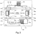
- a secure processor By placing the electronically conducting tracks or tamper revealing signals in specific patterns, mesh, a secure area is created. This is illustrated in Fig. 2 , which is a diagram illustrating the arrangement of electronic components and electrically conductive tracks within a security module 100 according to an embodiment of the invention.
- a first mesh 105 and a third mesh 107 are provided in the frame PCB 102, while a second mesh 106 is provided in the lid PCB 103.
- the first, second and third meshes 105, 106, 107 each have two electrically conductive tracks, and two tamper detection paths 108, 109 are formed from serial connections of the mesh tracks.
- each of the tamper detection paths 108, 109 comprises a serial connection of one track from each of the first, second and third meshes 105, 106, 107.
- a fourth mesh 110 is provided in the base PCB 101, where the fourth mesh 110 also has two electrically conductive tracks, and that each of the two tamper detection paths 108, 109 further comprises a track from the fourth mesh 110, where the fourth mesh track 110 may be electrically connected to the third mesh track 107 to thereby be in serial connection with the tracks from the first, second and third meshes 105, 106, 107.
- the security module 100 further comprises security circuitry 111, such as a processor, arranged on the top of the base PCB 101 within the protective space 104.
- the security circuitry 111 has two pairs of electrical signal input/outputs 112a, 112b and 113a, 113b, with the first input/outputs 112a, 112b connected to the first tamper detection path 108 and the second input/outputs 113a, 113 b connected to the second tamper detection path109 via the first mesh track 105 and the third or fourth mesh track 107 or 110.
- the conductive tracks of the fourth mesh 110 should at least partly be arranged below the security circuitry 111. As illustrated in Fig. 2 , part of or all of the conductive tracks of the meshes 105, 106, 107, 110 may comprise a serpentine track pattern.
- the connections between the electrically conductive tracks or meshes, 105, 106, 107, 110 of the different PCBs 101, 102, 103 are provided via electrical mesh contact points arranged at the top and/or bottom of the corresponding PCB.
- This is illustrated in Fig. 2 , in which there are four electrical contact points 114a,b,c,d on the top of the base PCB 101, four electrical contact points 115a,b,c,d on the bottom of the frame PCB 102, four electrical contact points 116a,b,c,d on the top of the frame PCB 102, and four electrical contact points 117a,b,c,d on the bottom of the lid PCB 103.
- the connections for the first tamper detection path 108 is made by connections between contacts points 114a and 115a, between contact points 116a and 117a, between contact points 117b and 116b, and between contact points 115b and 114b.
- the connections for the second tamper detection path 109 is made by connections between contacts points 114c and 115c, between contact points 116c and 117c, between contact points 117d and 116d, and between contact points 115d and 114d.
- the electrical mesh contact points may be carbon contact points.
- Fig. 3 is a cross sectional view showing the electrical PCB stack-up of the security module 100 of Fig. 2 .
- the security module 100 holds both security circuitry or secure processor 111 and secure components 118, which are to be protected from unauthorized access.
- the PCBs 101, 102, 103 all hold four conductive track layers, where for the lid PCB 103, the two upper conductive layers are connected to ground, while the conductive tracks of the second mesh 106 are arranged in the two lower conductive track layers of the lid PCB 103.
- each of the four conductive track layers holds conductive tracks of the first and third meshes 105, 107.
- the base PCB 101 also holds four conductive track layers, where the third track layer when numbered from the top may hold conductive tracks of the fourth mesh 110, while the upper track layer may be used for placement and routing of the security circuitry 111 and the secure components 118.
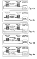
- the security circuitry 111 is adapted to detect if any of the conductive tracks within a tamper detection path 108 or 109, which is electrically connected to the security circuitry 111, is broken or comes into electrically contact with an electrically conductive track not being part of the tamper detection path 108 or 109. This is illustrated in Figs. 4a-4e , which show different operational states of the electronic circuitry illustrated in Fig. 2 . Fig. 4a illustrates the normal working state with no shorts or cuts in the tamper detection paths 18 and 109. Fig.
- FIG. 4b illustrates the situation when there is a cut in the first tamper detection path 108, whereby no signals can be forwarded between the corresponding input/outputs 112a, 112b of the secure processor 111, which is detected by the processor 111.
- Fig. 4c illustrates the situation when there is a cut in the second tamper detection path 109, whereby no signals can be forwarded between the corresponding input/outputs 113a, 113b of the secure processor 111, which is detected by the processor 111.
- Fig. 4d illustrates the situation when there is a short between the two tamper detection paths 108, 109, which will also be detected by the processor 111
- Fig. 4e illustrates the situation when there is a short between a tamper detection path 109 and ground, which is also to be detected by the processor 111.
- the mesh signals or tamper detection paths 108, 109 connect between the PCBs 101, 102, 103 through electrical mesh contact points 114, 115, 116, 117. It is preferred that the mesh contact points are placed closely to screws holding the security module 100 together. This may ensure that a mesh interruption or interruption of a detection path 108, 109 will occur if the screws are loosened.
- a preferred embodiment of the arrangement of a mesh contact point is illustrated in Fig. 5 , which shows the PCB layout of a corner region of a frame PCB 102 for use in the security module 100.
- FIG. 5 shows a fastening or screw hole 119 surrounded by a guard ring 120 and guard ring pieces 121, which guard ring 120 and guard ring pieces 121 are connected to a ground contact point 122.
- the electrical ground contact point 122 is arranged between the fastening hole 119 and the outer corner of the frame PCB 102.
- at least one of the meshes 105, 107 of the frame PCB 102 has conductive tracks 123 between the ground contact point 122 and the outer corner of the PCB 102.
- a mesh contact point 116a is arranged close to the fastening hole 119, opposite the ground contact point 122 and facing inwards from the fastening hole 119.
- the mesh contact point 116a is protected from the sides by guard ring pieces 124a, 124b, which are connected to ground, but the contact point 116a is also protected by the guard ring 120 surrounding the screw hole 119.
- the layout of the Fig. 5 also shows a mesh conductive track 125 connected to the contact point 116a and a mesh conductive track 126 connected through a via to a mesh conductive track of another layer of the frame PCB 102.
- the mesh contact point 116a is protected from the sides by guard ring pieces 124a,b and guard ring 120 with a different potential compared to the mesh signals.
- a short between the guard ring pieces 124a,b or guard ring 120 and the mesh contact point 116a will provide an intrusion alert to the processor 111.
- the layout is designed so that the mesh signal contact 116a is placed furthest away from the edge.
- the frame PCB 102 and the lid PCB 103 have four corner regions with mesh contact points arranged as illustrated in the layout of Fig. 5 .
- the frame PCB 102 this is illustrated in Fig. 6 , which shows a top view of a frame PCB 102 with four corner regions each holding one of the mesh contact points 116a, 116b, 116c, 116d.
- a bottom view of the frame PCB 102 of Fig 6 will have a similar look, with each of the corner regions holding one of the mesh contact points 115a, 115b, 115c, 115d.
- the mesh contacts point belonging to the same tamper detection path 108, 109 are arranged diagonally to each other.
- the lid PCB 103 the arrangement is illustrated in Fig. 7 , which shows a bottom view of a lid PCB 103 with four corner regions each holding one of the mesh contact points 117a, 117b, 117c, 117d.
- the base PCB 101 will be larger dimensioned than the frame and lid PCBs 102, 103, but in order to fit to the mesh contact points of the frame PCB 102, the four mesh contact points 114a, 114b, 114c, 114d are arranged correspondingly on top of the base PCB 101. This is shown in Fig. 8 .
- the PCB layout of the contacts points of the base PCB 101 may be similar to the layout described in Fig. 5 .
- the electrical ground contact points 122 are carbon contact points.
- Fig. 9 is a cross sectional view showing the PCB assembly of the security module 100
- Fig. 10 is a detailed view of a corner region of the PCB assembly of Fig. 9
- the base PCB 101, the frame PCB 102, and the lid PCB 103 are assembled by fastening means or screws 127 provided at the fastening holes 119 of each of the PCBs 101, 102, 103. From Fig. 10 it can be seen that the mesh contact points 114a, 115a and 116a, 117a, respectively, are brought into contact on one side of the hole 119, while the corresponding ground contact points 120 are brought into contact on the opposite side of the hole 119.
Landscapes
- Engineering & Computer Science (AREA)
- Microelectronics & Electronic Packaging (AREA)
- Computer Hardware Design (AREA)
- Computer Security & Cryptography (AREA)
- Theoretical Computer Science (AREA)
- General Physics & Mathematics (AREA)
- Physics & Mathematics (AREA)
- General Engineering & Computer Science (AREA)
- Software Systems (AREA)
- Shielding Devices Or Components To Electric Or Magnetic Fields (AREA)
- Burglar Alarm Systems (AREA)
- Storage Device Security (AREA)
- Casings For Electric Apparatus (AREA)
Description
- The present invention relates to the field of electronic circuit protection, and especially to a security module for protecting circuit components from unauthorized access. The security module includes a printed circuit board assembly.
- In certain applications, for example payment card systems, it is necessary to provide some physical security to prevent unauthorized access to a circuit and more particularly to data contained within memory devices in a circuit.
- This may conventionally be achieved by placement of the circuit to be protected within an enclosure. To enhance the mechanical security provided by these enclosures, detected interference with the enclosure triggers the protected circuit to perform one or more specific actions, including for example setting off an alarm and/or encrypting or erasing the data stored in circuit memory devices.
- On method of detecting interference is to surround the circuit with one or more patterns of conductors. These conductors may be arranged in a mesh so that any person attempting to interfere with the enclosure will break one or more of the conductors. Appropriate sensing circuitry is provided to detect a break in a conductor. Such a method and system is exemplified by
US 7,475,474 B2 and byDE 10 2008 057 887 A1 . The security system disclosed inDE 10 2008 057 887 A1 has mesh conductor tracks formed into layers of upper, middle and lower printed circuit boards, where sensing circuitry is provided in a protection zone formed by the middle printed circuit board. - The security module according to the present invention, which includes a printed circuit board assembly, provides a cost effective solution to the problem of protecting electronic components from unwanted access
- According to the present invention there is provided a security module for protecting circuit components from unauthorized access, the module comprising:
- a base printed circuit board, base PCB, for supporting circuit components to be protected;
- a frame printed circuit board, frame PCB, said frame PCB being secured on top of the base PCB and defining a protective space for circuit components supported by the base PCB;
- a lid printed circuit board, lid PCB, being secured on top of the frame PCB, thereby providing a top closure to the protective space;
- first and third meshes provided in the frame PCB;
- a second mesh provided in the lid PCB; and
- a fourth mesh provided in the base PCB;
- The security circuitry may be arranged on top of the base PCB. It is preferred that the conductive track(s) of the fourth mesh is/are at least partly arranged below the security circuitry.
- According to one or more embodiments of the invention, then part of or all of the conductive tracks of the meshes comprises a serpentine track pattern.
- It is preferred that for each tamper detection path the connections between electrically conductive tracks of different PCBs are provided via electrical mesh contact points arranged at the top and/or bottom of the corresponding PCB. It is also preferred that for each tamper detection path, two electrical mesh contact points are provided on top of the base PCB, two corresponding electrical mesh contact points are provided at the bottom of the frame PCB, two corresponding electrical mesh contact points are provided at the top of the frame PCB, and two corresponding electrical mesh contact points are provided at the bottom of the lid PCB.
- According to an embodiment of the invention, the security module comprises two tamper detection paths, with four electrical mesh contact points provided on top of the base PCB, four corresponding electrical mesh contact points provided at the bottom of the frame PCB, four corresponding electrical mesh contact points provided at the top of the frame PCB, and four corresponding electrical mesh contact points provided at the bottom of the lid PCB.
- The electrical mesh contact points may be carbon contact points.
- According to one or more embodiments of the invention then the electrical mesh contact points are at least partly surrounded by one or more guard ring pieces being connected to ground.
- The present invention also covers one or more embodiments, wherein the frame PCB and the lid PCB have four corner regions with a mesh contact point arranged in each corner region, and wherein four mesh contact points are correspondingly arranged on top of the base PCB. It is also within one or more embodiments of the invention that fastening holes are provided in each corner region of the frame PCB and the lid PCB, and that corresponding fastening holes are provided in the base PCB. Here, fastening means may be provided at the fastening holes for securing the frame PCB and the lid PCB to the base PCB. For the frame PCB and the lid PCB it is preferred that a fastening hole is placed between the mesh contact point and the outer corner of the PCB. It is also preferred that for part of or for each fastening hole in the frame PCB and the lid PCB, an electrical ground contact point is provided between the fastening hole and the outer corner of the PCB. For each fastening hole of the base PCB, a mesh contact point may be arranged facing inwards from the fastening hole and an electrical ground contact point may be provided on the opposite side of the fastening hole. It is preferred that the electrical ground contact points are carbon contact points.
- The conductive tracks of the meshes may be arranged in several track layers with the corresponding PCBs. Thus, the second mesh may comprise electrically conductive tracks arranged in two track layers of the lid PCB. The lid PCB may hold four conductive track layers, with the two upper track layers being connected to ground, and with the two lower track layers holding the conductive tracks of the second mesh. For the frame PCB, the frame PCB may hold four conductive track layers, where each of the track layers may hold conductive tracks of the first and third meshes. Also the base PCB may hold four conductive track layers, where the third track layer when numbered from the top may hold conductive tracks of the fourth mesh.
- For embodiments holding security circuitry, the security circuitry may be adapted to detect if any of the conductive tracks within a tamper detection path, which is electrically connected to the security circuitry, is broken or comes into electrically contact with an electrically conductive track not being part of said tamper detection path.
-
-
Fig. 1 shows three circuit boards of a security module according to an embodiment of the invention, -
Fig. 2 is a diagram illustrating the arrangement of electronic components and electrically conductive tracks within a security module according to an embodiment of the invention, -
Fig. 3 is a cross sectional view of a security module according to an embodiment of the invention, -
Figs. 4a-4e illustrate different operational states of the electronic circuitry illustrated inFig. 2 , -
Fig. 5 shows the PCB layout of a corner region of a frame PCB for use in a security module according to an embodiment of the invention, -
Fig. 6 is a top view of a frame PCB for use in a security module according to an embodiment of the invention, -
Fig. 7 is a bottom view of a lid PCB for use in a security module according to an embodiment of the invention, -
Fig. 8 is a top view of a base PCB for use in a security module according to an embodiment of the invention, -
Fig. 9 is a cross sectional view showing the PCB assembly of a security module according to an embodiment of the invention, and -
Fig. 10 is a detailed view of a corner region of the PCB assembly ofFig. 9 . - The present invention provides a security module for protecting circuit components from unauthorized access. The security module includes a printed circuit assembly, which holds a secure area for protecting circuit components from unauthorized access. In a preferred embodiment, the security module of the invention comprises three printed circuit boards, PCBs. This is illustrated in
Fig. 1 , which shows the three PCBs of the security module: a base printedcircuit board 101, base PCB, for supporting circuit components to be protected, a frame printedcircuit board 102, frame PCB, and a lid printedcircuit board 103, lid PCB. The frame PCB 102 is designed to be secured on top of the base PCB 101, and the lid PCB 103 is designed to be secured on top of the frame PCB 102. When assembled, the threePCBs secure area 104, in which circuit components supported by the base PCB 101 can be arranged. The PBCs, 101, 102, 103, may assembled or fastened together by means (ie screws, brackets or similar) in at least four contact areas, which may include the four corner regions of theframe PCB 102 and the lid PCB 103. Intrusion detection is implemented by placing electronically conducting tracks (mesh) on and in some or all of thePCBs PCBs secure area 104, and the processor may sense different forms of tamper through the signaling in the tracks or meshes. - The combination of the
PCBs Fig. 2 , which is a diagram illustrating the arrangement of electronic components and electrically conductive tracks within asecurity module 100 according to an embodiment of the invention. - For the
security module 100 ofFig. 2 , afirst mesh 105 and athird mesh 107 are provided in theframe PCB 102, while asecond mesh 106 is provided in thelid PCB 103. The first, second andthird meshes tamper detection paths tamper detection paths third meshes fourth mesh 110 is provided in thebase PCB 101, where thefourth mesh 110 also has two electrically conductive tracks, and that each of the twotamper detection paths fourth mesh 110, where thefourth mesh track 110 may be electrically connected to thethird mesh track 107 to thereby be in serial connection with the tracks from the first, second andthird meshes tamper detecting path security module 100 further comprisessecurity circuitry 111, such as a processor, arranged on the top of thebase PCB 101 within theprotective space 104. Thesecurity circuitry 111 has two pairs of electrical signal input/outputs outputs tamper detection path 108 and the second input/outputs first mesh track 105 and the third orfourth mesh track - For secure modules according to the invention comprising the
fourth mesh 110, the conductive tracks of thefourth mesh 110 should at least partly be arranged below thesecurity circuitry 111. As illustrated inFig. 2 , part of or all of the conductive tracks of themeshes - For each
tamper detection path different PCBs Fig. 2 , in which there are fourelectrical contact points 114a,b,c,d on the top of thebase PCB 101, fourelectrical contact points 115a,b,c,d on the bottom of theframe PCB 102, fourelectrical contact points 116a,b,c,d on the top of theframe PCB 102, and fourelectrical contact points 117a,b,c,d on the bottom of thelid PCB 103. The connections for the firsttamper detection path 108 is made by connections between contacts points 114a and 115a, betweencontact points tamper detection path 109 is made by connections between contacts points 114c and 115c, between contact points 116c and 117c, betweencontact points contact points -
Fig. 3 is a cross sectional view showing the electrical PCB stack-up of thesecurity module 100 ofFig. 2 . InFig. 3 thesecurity module 100 holds both security circuitry orsecure processor 111 andsecure components 118, which are to be protected from unauthorized access. ThePCBs lid PCB 103, the two upper conductive layers are connected to ground, while the conductive tracks of thesecond mesh 106 are arranged in the two lower conductive track layers of thelid PCB 103. For the frame PCB, each of the four conductive track layers holds conductive tracks of the first andthird meshes base PCB 101 also holds four conductive track layers, where the third track layer when numbered from the top may hold conductive tracks of thefourth mesh 110, while the upper track layer may be used for placement and routing of thesecurity circuitry 111 and thesecure components 118. - The
security circuitry 111 is adapted to detect if any of the conductive tracks within atamper detection path security circuitry 111, is broken or comes into electrically contact with an electrically conductive track not being part of thetamper detection path Figs. 4a-4e , which show different operational states of the electronic circuitry illustrated inFig. 2 .Fig. 4a illustrates the normal working state with no shorts or cuts in thetamper detection paths 18 and 109.Fig. 4b illustrates the situation when there is a cut in the firsttamper detection path 108, whereby no signals can be forwarded between the corresponding input/outputs secure processor 111, which is detected by theprocessor 111. Similarly,Fig. 4c illustrates the situation when there is a cut in the secondtamper detection path 109, whereby no signals can be forwarded between the corresponding input/outputs secure processor 111, which is detected by theprocessor 111.Fig. 4d illustrates the situation when there is a short between the twotamper detection paths processor 111, andFig. 4e illustrates the situation when there is a short between atamper detection path 109 and ground, which is also to be detected by theprocessor 111. - The mesh signals or
tamper detection paths PCBs security module 100 together. This may ensure that a mesh interruption or interruption of adetection path Fig. 5 , which shows the PCB layout of a corner region of aframe PCB 102 for use in thesecurity module 100. - The layout of
Fig. 5 shows a fastening orscrew hole 119 surrounded by aguard ring 120 andguard ring pieces 121, whichguard ring 120 andguard ring pieces 121 are connected to aground contact point 122. The electricalground contact point 122 is arranged between thefastening hole 119 and the outer corner of theframe PCB 102. Furthermore, at least one of themeshes frame PCB 102 hasconductive tracks 123 between theground contact point 122 and the outer corner of thePCB 102. Amesh contact point 116a is arranged close to thefastening hole 119, opposite theground contact point 122 and facing inwards from thefastening hole 119. Themesh contact point 116a is protected from the sides byguard ring pieces contact point 116a is also protected by theguard ring 120 surrounding thescrew hole 119. The layout of theFig. 5 also shows a meshconductive track 125 connected to thecontact point 116a and a meshconductive track 126 connected through a via to a mesh conductive track of another layer of theframe PCB 102. - For the layout in
Fig. 5 , themesh contact point 116a is protected from the sides byguard ring pieces 124a,b andguard ring 120 with a different potential compared to the mesh signals. A short between theguard ring pieces 124a,b orguard ring 120 and themesh contact point 116a will provide an intrusion alert to theprocessor 111. The layout is designed so that themesh signal contact 116a is placed furthest away from the edge. - For the preferred embodiment of the
security module 100, theframe PCB 102 and thelid PCB 103 have four corner regions with mesh contact points arranged as illustrated in the layout ofFig. 5 . For theframe PCB 102, this is illustrated inFig. 6 , which shows a top view of aframe PCB 102 with four corner regions each holding one of themesh contact points frame PCB 102 ofFig 6 will have a similar look, with each of the corner regions holding one of themesh contact points tamper detection path lid PCB 103, the arrangement is illustrated inFig. 7 , which shows a bottom view of alid PCB 103 with four corner regions each holding one of themesh contact points - Usually, the
base PCB 101 will be larger dimensioned than the frame andlid PCBs frame PCB 102, the fourmesh contact points base PCB 101. This is shown inFig. 8 . The PCB layout of the contacts points of thebase PCB 101 may be similar to the layout described inFig. 5 . It is noted that for each of themesh contact points 114a,b,c,d, 115a,b,c,d, 116a,b,c,d and 117a,b,c,d, there are correspondingguard ring pieces 124a,b, and there is afastening hole 119 with acorresponding guard ring 120 andguard ring pieces 121 and a correspondingground contact point 122. - It is preferred that the electrical ground contact points 122 are carbon contact points.
-
Fig. 9 is a cross sectional view showing the PCB assembly of thesecurity module 100, andFig. 10 is a detailed view of a corner region of the PCB assembly ofFig. 9 . Thebase PCB 101, theframe PCB 102, and thelid PCB 103, are assembled by fastening means or screws 127 provided at the fastening holes 119 of each of thePCBs Fig. 10 it can be seen that themesh contact points hole 119, while the corresponding ground contact points 120 are brought into contact on the opposite side of thehole 119.
wherein at least two tamper detection paths are formed with each of said at least two tamper detection paths comprising a serial connection of one track from each of the first, second, third and fourth meshes, thereby comprising a track from the first mesh, which is electrically connected to a track from the second mesh, which again is electrically connected to a track from the third mesh, which again is electrically connected to a track from the fourth mesh;
and wherein for each of said at least two tamper detection paths the security circuitry has a pair of electrical signal input/outputs being electrically connected to the tamper detection path via the first mesh track and the fourth mesh track of said tamper detection path.
Claims (21)
- A security module (100) for protecting circuit components from unauthorized access, the module comprising:- a base printed circuit board, base PCB (101), for supporting circuit components to be protected;- a frame printed circuit board, frame PCB (102), said frame PCB (102) being secured on top of the base PCB (101) and defining a protective space (104) for circuit components (111, 118) supported by the base PCB (101);- a lid printed circuit board, lid PCB (103), being secured on top of the frame PCB (102), thereby providing a top closure to the protective space (104);- security circuitry (111) arranged on the base PCB within said protective space (104);- first and third meshes (105, 107) provided in the frame PCB (102);- a second mesh (106) provided in the lid PCB (103); and- a fourth mesh (110) provided in the base PCB (101); characterized in that the first, second, third and fourth meshes (105, 106, 107, 110) have at least two electrically conductive tracks; whereinat least two tamper detection paths (108, 109) are formed with each of said at least two tamper detection paths (108, 109) comprising a serial connection of one track from each of the first, second, third and fourth meshes (105, 106, 107, 110), thereby comprising a track from the first mesh (105), which is electrically connected to a track from the second mesh (106), which again is electrically connected to a track from the third mesh (107), which again is electrically connected to a track from the fourth mesh (110); and in that
for each of said at least two tamper detection paths (108, 109) the security circuitry (111) has a pair of electrical signal input/outputs (112a, 113a, 112b, 113b) being electrically connected to the tamper detection path (108, 109) via the first mesh track (105) and the fourth mesh track (110) of said tamper detection path (108, 109). - A security module (100) according to claim 1, wherein the security circuitry (111) is arranged on top of the base PCB (101).
- A security module (100) according to claim 1 or 2, wherein the conductive track(s) of the fourth mesh (110) is/are at least partly arranged below the security circuitry (111).
- A security module (100) according to any one of the claims 1-3, wherein part of or all of the conductive tracks of the meshes (105, 106, 107, 110) comprises a serpentine track pattern.
- A security module (100) according to any one of the claims 1-4, wherein for each tamper detection path (108, 109) the connections between electrically conductive tracks of different PCBs (101, 102, 103) are provided via electrical mesh contact points (114a,b,c,d, 115a,b,c,d, 116a,b,c,d, 117a,b,c,d) arranged at the top and/or bottom of the corresponding PCB (101, 102, 103).
- A security module (100) according to any one of the claims 1-5, wherein for each tamper detection path (108, 109), two electrical mesh contact points (114a,b,c,d) are provided on top of the base PCB (101), two corresponding electrical mesh contact points (115a,b,c,d) are provided at the bottom of the frame PCB (102), two corresponding electrical mesh contact points (116a,b,c,d) are provided at the top of the frame PCB (102), and two corresponding electrical mesh contact points (117a,b,c,d) are provided at the bottom of the lid PCB (103).
- A security module (100) according to any one of the claims 1-6, wherein the security module (100) comprises two tamper detection paths (108, 109), with four electrical mesh contact points (114a,b,c,d) provided on top of the base PCB (101), four corresponding electrical mesh contact points (115a,b,c,d) provided at the bottom of the frame PCB (102), four corresponding electrical mesh contact points (116a,b,c,d) provided at the top of the frame PCB (102), and four corresponding electrical mesh contact points (117a,b,c,d) provided at the bottom of the lid PCB (103).
- A security module (100) according to any one of the claims 5-7, wherein the electrical mesh contact points (114a,b,c,d, 115a,b,c,d, 116a,b,c,d, 117a,b,c,d) are carbon contact points.
- A security module (100) according to any one of the claims 5-8, wherein the electrical mesh contact points (114a,b,c,d, 115a,b,c,d, 116a,b,c,d, 117a,b,c,d) are at least partly surrounded by one or more guard ring pieces (120, 121) being connected to ground.
- A security module (100) according to any one of the claims 5-9, wherein the frame PCB (102) and the lid PCB (103) have four corner regions with a mesh contact point (115a,b,c,d, 116a,b,c,d, 117a,b,c,d) arranged in each corner region, and wherein four mesh contact points (114a,b,c,d) are correspondingly arranged on top of the base PCB (101).
- A security module (100) according to any one of the claims 1-10, wherein fastening holes (119) are provided in each corner region of the frame PCB (102) and the lid PCB (103) with corresponding fastening holes (119) being provided in the base PCB (101).
- A security module (100) according to claim 11, wherein fastening means (127) are provided at said fastening holes (119) for securing the frame PCB (102) and the lid PCB (103) to the base PCB (101).
- A security module (100) according to claim 10 and 11 or 12, wherein for the frame PCB (102) and the lid PCB (103) a fastening hole (119) is placed between the mesh contact point (115a,b,c,d, 116a,b,c,d, 117a,b,c,d) and the outer corner of the PCB (102, 103).
- A security module (100) according to any one of the claims 11-13, wherein for part of or for each fastening hole (119) in the frame PCB (102) and the lid PCB (103) an electrical ground contact point (122) is provided between the fastening hole and (119) the outer corner of the PCB (102, 103).
- A security module (100) according to claim 14, wherein for each fastening hole (119) of the base PCB (101), a mesh contact point (114,a,b,c,d) is arranged facing inwards from the fastening hole (119) and an electrical ground contact point (122) is provided on the opposite side of the fastening hole (119).
- A security module (100) according to claim 14 or 15, wherein the electrical ground contact points(122) are carbon contact points.
- A security module (100) according to any one of the claims 1-16, wherein the second mesh (106) comprises electrically conductive tracks arranged in two track layers of the lid PCB (103).
- A security module (100) according to claim 17, wherein the lid PCB (103) holds four conductive track layers, with the two upper track layers being connected to ground, and with the two lower track layers holding the conductive tracks of the second mesh (106).
- A security module (100) according to any one of the claims 1-18, wherein the frame PCB (102) holds four conductive track layers, each of which holds conductive tracks of the first and third meshes (105, 107).
- A security module (100) according to any one of the claims 1-19, wherein the base PCB (101) holds four conductive track layers, with the third track layer when numbered from the top holding conductive tracks of the fourth mesh (110).
- A security module (100) according to any one of the claims 1-20, wherein the security circuitry (111) is adapted to detect if any of the conductive tracks within a tamper detection path (108, 109) being electrically connected to the security circuitry (111) is broken or comes into electrically contact with an electrically conductive track not being part of said tamper detection path (108, 109).
Applications Claiming Priority (2)
| Application Number | Priority Date | Filing Date | Title |
|---|---|---|---|
| DKPA201200774 | 2012-12-07 | ||
| PCT/EP2013/075834 WO2014086987A2 (en) | 2012-12-07 | 2013-12-06 | A security module for protecting circuit components from unauthorized access |
Publications (2)
| Publication Number | Publication Date |
|---|---|
| EP2929482A2 EP2929482A2 (en) | 2015-10-14 |
| EP2929482B1 true EP2929482B1 (en) | 2018-05-02 |
Family
ID=49753166
Family Applications (1)
| Application Number | Title | Priority Date | Filing Date |
|---|---|---|---|
| EP13802611.7A Active EP2929482B1 (en) | 2012-12-07 | 2013-12-06 | A security module for protecting circuit components from unauthorized access |
Country Status (4)
| Country | Link |
|---|---|
| US (1) | US10009995B2 (en) |
| EP (1) | EP2929482B1 (en) |
| CN (1) | CN105051751B (en) |
| WO (1) | WO2014086987A2 (en) |
Families Citing this family (36)
| Publication number | Priority date | Publication date | Assignee | Title |
|---|---|---|---|---|
| US9560737B2 (en) | 2015-03-04 | 2017-01-31 | International Business Machines Corporation | Electronic package with heat transfer element(s) |
| FR3037764B1 (en) * | 2015-06-16 | 2018-07-27 | Ingenico Group | SENSITIVE SIGNAL PROTECTION COMPONENT, DEVICE AND CORRESPONDING METHOD |
| US10426037B2 (en) | 2015-07-15 | 2019-09-24 | International Business Machines Corporation | Circuitized structure with 3-dimensional configuration |
| US9924591B2 (en) | 2015-09-25 | 2018-03-20 | International Business Machines Corporation | Tamper-respondent assemblies |
| US9894749B2 (en) | 2015-09-25 | 2018-02-13 | International Business Machines Corporation | Tamper-respondent assemblies with bond protection |
| US10098235B2 (en) | 2015-09-25 | 2018-10-09 | International Business Machines Corporation | Tamper-respondent assemblies with region(s) of increased susceptibility to damage |
| US10175064B2 (en) | 2015-09-25 | 2019-01-08 | International Business Machines Corporation | Circuit boards and electronic packages with embedded tamper-respondent sensor |
| US9591776B1 (en) | 2015-09-25 | 2017-03-07 | International Business Machines Corporation | Enclosure with inner tamper-respondent sensor(s) |
| US9578764B1 (en) | 2015-09-25 | 2017-02-21 | International Business Machines Corporation | Enclosure with inner tamper-respondent sensor(s) and physical security element(s) |
| US9911012B2 (en) | 2015-09-25 | 2018-03-06 | International Business Machines Corporation | Overlapping, discrete tamper-respondent sensors |
| US10172239B2 (en) | 2015-09-25 | 2019-01-01 | International Business Machines Corporation | Tamper-respondent sensors with formed flexible layer(s) |
| US10143090B2 (en) | 2015-10-19 | 2018-11-27 | International Business Machines Corporation | Circuit layouts of tamper-respondent sensors |
| US9978231B2 (en) | 2015-10-21 | 2018-05-22 | International Business Machines Corporation | Tamper-respondent assembly with protective wrap(s) over tamper-respondent sensor(s) |
| FR3043231B1 (en) * | 2015-11-03 | 2017-12-22 | Ingenico Group | MEMORY CARD READER BODY WITH TWO-SIDED PROTECTION LATCH |
| US9913389B2 (en) | 2015-12-01 | 2018-03-06 | International Business Corporation Corporation | Tamper-respondent assembly with vent structure |
| US10327343B2 (en) | 2015-12-09 | 2019-06-18 | International Business Machines Corporation | Applying pressure to adhesive using CTE mismatch between components |
| US9555606B1 (en) | 2015-12-09 | 2017-01-31 | International Business Machines Corporation | Applying pressure to adhesive using CTE mismatch between components |
| US9554477B1 (en) | 2015-12-18 | 2017-01-24 | International Business Machines Corporation | Tamper-respondent assemblies with enclosure-to-board protection |
| US9916744B2 (en) | 2016-02-25 | 2018-03-13 | International Business Machines Corporation | Multi-layer stack with embedded tamper-detect protection |
| US9904811B2 (en) | 2016-04-27 | 2018-02-27 | International Business Machines Corporation | Tamper-proof electronic packages with two-phase dielectric fluid |
| US9913370B2 (en) | 2016-05-13 | 2018-03-06 | International Business Machines Corporation | Tamper-proof electronic packages formed with stressed glass |
| US9881880B2 (en) | 2016-05-13 | 2018-01-30 | International Business Machines Corporation | Tamper-proof electronic packages with stressed glass component substrate(s) |
| CN107426926B (en) * | 2016-05-24 | 2019-08-27 | 鸿富锦精密工业(深圳)有限公司 | Anti-dismantle mechanism and electronic device with the anti-dismantle mechanism |
| US9858776B1 (en) | 2016-06-28 | 2018-01-02 | International Business Machines Corporation | Tamper-respondent assembly with nonlinearity monitoring |
| US10321589B2 (en) | 2016-09-19 | 2019-06-11 | International Business Machines Corporation | Tamper-respondent assembly with sensor connection adapter |
| US10299372B2 (en) | 2016-09-26 | 2019-05-21 | International Business Machines Corporation | Vented tamper-respondent assemblies |
| US10271424B2 (en) | 2016-09-26 | 2019-04-23 | International Business Machines Corporation | Tamper-respondent assemblies with in situ vent structure(s) |
| US9999124B2 (en) | 2016-11-02 | 2018-06-12 | International Business Machines Corporation | Tamper-respondent assemblies with trace regions of increased susceptibility to breaking |
| US10327329B2 (en) | 2017-02-13 | 2019-06-18 | International Business Machines Corporation | Tamper-respondent assembly with flexible tamper-detect sensor(s) overlying in-situ-formed tamper-detect sensor |
| US10306753B1 (en) | 2018-02-22 | 2019-05-28 | International Business Machines Corporation | Enclosure-to-board interface with tamper-detect circuit(s) |
| US11122682B2 (en) | 2018-04-04 | 2021-09-14 | International Business Machines Corporation | Tamper-respondent sensors with liquid crystal polymer layers |
| EP3604049B1 (en) * | 2018-08-03 | 2022-10-05 | Aptiv Technologies Limited | Secure vehicle control unit |
| US10925154B2 (en) * | 2019-01-31 | 2021-02-16 | Texas Instruments Incorporated | Tamper detection |
| US10595401B1 (en) | 2019-05-29 | 2020-03-17 | International Business Machines Corporation | Tamper detection at enclosure-to-board interface |
| CN110674536B (en) * | 2019-08-16 | 2021-08-13 | 华为技术有限公司 | Anti-disassembly device and electronic equipment of security chip |
| WO2022067049A1 (en) * | 2020-09-24 | 2022-03-31 | Sumup Payments Ltd. | Communication system and display synchronization |
Citations (1)
| Publication number | Priority date | Publication date | Assignee | Title |
|---|---|---|---|---|
| DE102008057887A1 (en) * | 2008-11-18 | 2010-05-20 | Francotyp-Postalia Gmbh | Cryptographic module i.e. postal safety module, for use in franking machine, has access-protection unit consisting of printed circuit boards, where conductor paths of boards are changed from one layer to another layer |
Family Cites Families (16)
| Publication number | Priority date | Publication date | Assignee | Title |
|---|---|---|---|---|
| GB9101207D0 (en) * | 1991-01-18 | 1991-02-27 | Ncr Co | Data security device |
| GB0012478D0 (en) * | 2000-05-24 | 2000-07-12 | Ibm | Intrusion detection mechanism for cryptographic cards |
| EP1421549B1 (en) | 2001-08-31 | 2007-08-22 | VeriFone Systems Ireland Limited | A pin pad |
| US6853093B2 (en) * | 2002-12-20 | 2005-02-08 | Lipman Electronic Engineering Ltd. | Anti-tampering enclosure for electronic circuitry |
| US7180008B2 (en) | 2004-01-23 | 2007-02-20 | Pitney Bowes Inc. | Tamper barrier for electronic device |
| US7281667B2 (en) * | 2005-04-14 | 2007-10-16 | International Business Machines Corporation | Method and structure for implementing secure multichip modules for encryption applications |
| US20070177363A1 (en) | 2006-01-31 | 2007-08-02 | Symbol Technologies, Inc. | Multilayer printed circuit board having tamper detection circuitry |
| FR2901896B1 (en) | 2006-06-02 | 2008-10-31 | Sagem Monetel Soc Par Actions | DEVICE FOR PROTECTION AGAINST INTRUSIONS OF ELECTRONIC APPARATUS |
| US7923830B2 (en) * | 2007-04-13 | 2011-04-12 | Maxim Integrated Products, Inc. | Package-on-package secure module having anti-tamper mesh in the substrate of the upper package |
| US7615416B1 (en) * | 2007-08-31 | 2009-11-10 | Maxim Integrated Products, Inc. | Secure package with anti-tamper peripheral guard ring |
| US7791194B2 (en) * | 2008-04-10 | 2010-09-07 | Oracle America, Inc. | Composite interconnect |
| CN201233600Y (en) * | 2008-05-19 | 2009-05-06 | 福建联迪商用设备有限公司 | Protection apparatus for sensitive data anti-theft |
| US8325486B2 (en) * | 2009-01-13 | 2012-12-04 | Dy 4 Systems Inc. | Tamper respondent module |
| CN101615235A (en) * | 2009-08-04 | 2009-12-30 | 青岛海信智能商用设备有限公司 | A kind of self-destruction system for memory data |
| US8238095B2 (en) | 2009-08-31 | 2012-08-07 | Ncr Corporation | Secure circuit board assembly |
| CN201532635U (en) * | 2009-09-03 | 2010-07-21 | 百富计算机技术(深圳)有限公司 | A safety protection device |
-
2013
- 2013-12-06 CN CN201380064156.XA patent/CN105051751B/en active Active
- 2013-12-06 US US14/649,848 patent/US10009995B2/en active Active
- 2013-12-06 WO PCT/EP2013/075834 patent/WO2014086987A2/en not_active Ceased
- 2013-12-06 EP EP13802611.7A patent/EP2929482B1/en active Active
Patent Citations (1)
| Publication number | Priority date | Publication date | Assignee | Title |
|---|---|---|---|---|
| DE102008057887A1 (en) * | 2008-11-18 | 2010-05-20 | Francotyp-Postalia Gmbh | Cryptographic module i.e. postal safety module, for use in franking machine, has access-protection unit consisting of printed circuit boards, where conductor paths of boards are changed from one layer to another layer |
Also Published As
| Publication number | Publication date |
|---|---|
| CN105051751B (en) | 2019-01-01 |
| CN105051751A (en) | 2015-11-11 |
| WO2014086987A2 (en) | 2014-06-12 |
| US10009995B2 (en) | 2018-06-26 |
| US20150382455A1 (en) | 2015-12-31 |
| WO2014086987A3 (en) | 2014-07-31 |
| EP2929482A2 (en) | 2015-10-14 |
Similar Documents
| Publication | Publication Date | Title |
|---|---|---|
| EP2929482B1 (en) | A security module for protecting circuit components from unauthorized access | |
| US7180008B2 (en) | Tamper barrier for electronic device | |
| CN103578201B (en) | Safety guard and the method for being formed and installing the device | |
| US10078764B2 (en) | Tamper responsive sensor | |
| US9450586B2 (en) | Security shield assembly | |
| WO2013162843A1 (en) | Tamper respondent covering | |
| EP2330528B1 (en) | Secure circuit board assembly | |
| US9055672B2 (en) | Device for protecting an electronic printed circuit board | |
| US8223503B2 (en) | Security cover for protecting the components mounted on a printed circuit board (PCB) against being attached | |
| JP2018530056A (en) | Circuit board and electronic package including embedded tamper sensitive sensor | |
| US20130142327A1 (en) | Anti-spying encrypted keyboard | |
| US8270174B2 (en) | Hardware protection system for sensitive electronic-data modules protecting against external manipulations | |
| US20110255253A1 (en) | Protective serpentine track for card payment terminal | |
| CN101128094B (en) | Secure protection device | |
| US20190097302A1 (en) | Patch antenna layer for tamper event detection | |
| JP4740327B2 (en) | Sensor for hardware protection device of sensitive electronic device data module against unauthorized manipulation from outside | |
| CN210924786U (en) | Two-sided protection apron of POS machine | |
| EP2931011A1 (en) | A safety box for electronic circuit protection | |
| EP3574721B1 (en) | An electronic sensitive zone protection system | |
| BR102021006577A2 (en) | SYSTEM FOR CONNECTOR PROTECTION FOR SMART CARDS IN EQUIPMENT THAT REQUIRE DATA SECURITY | |
| CN111028443A (en) | A double-sided protective cover for a POS machine | |
| BRPI1101001A2 (en) | method of mechanical and electronic protection of safety equipment based on plates and tapes | |
| BR102019004819A2 (en) | SHIELDING SYSTEM FOR TAX MODULES | |
| BRPI1101244A2 (en) | smart card connector protection system for data security equipment |
Legal Events
| Date | Code | Title | Description |
|---|---|---|---|
| PUAI | Public reference made under article 153(3) epc to a published international application that has entered the european phase |
Free format text: ORIGINAL CODE: 0009012 |
|
| 17P | Request for examination filed |
Effective date: 20150707 |
|
| AK | Designated contracting states |
Kind code of ref document: A2 Designated state(s): AL AT BE BG CH CY CZ DE DK EE ES FI FR GB GR HR HU IE IS IT LI LT LU LV MC MK MT NL NO PL PT RO RS SE SI SK SM TR |
|
| AX | Request for extension of the european patent |
Extension state: BA ME |
|
| DAX | Request for extension of the european patent (deleted) | ||
| 17Q | First examination report despatched |
Effective date: 20160428 |
|
| REG | Reference to a national code |
Ref country code: DE Ref legal event code: R079 Ref document number: 602013036979 Country of ref document: DE Free format text: PREVIOUS MAIN CLASS: G06F0021750000 Ipc: H05K0001020000 |
|
| GRAP | Despatch of communication of intention to grant a patent |
Free format text: ORIGINAL CODE: EPIDOSNIGR1 |
|
| RIC1 | Information provided on ipc code assigned before grant |
Ipc: H05K 1/02 20060101AFI20171110BHEP |
|
| INTG | Intention to grant announced |
Effective date: 20171129 |
|
| GRAS | Grant fee paid |
Free format text: ORIGINAL CODE: EPIDOSNIGR3 |
|
| GRAA | (expected) grant |
Free format text: ORIGINAL CODE: 0009210 |
|
| AK | Designated contracting states |
Kind code of ref document: B1 Designated state(s): AL AT BE BG CH CY CZ DE DK EE ES FI FR GB GR HR HU IE IS IT LI LT LU LV MC MK MT NL NO PL PT RO RS SE SI SK SM TR |
|
| REG | Reference to a national code |
Ref country code: GB Ref legal event code: FG4D |
|
| REG | Reference to a national code |
Ref country code: AT Ref legal event code: REF Ref document number: 996621 Country of ref document: AT Kind code of ref document: T Effective date: 20180515 Ref country code: CH Ref legal event code: EP |
|
| REG | Reference to a national code |
Ref country code: DE Ref legal event code: R096 Ref document number: 602013036979 Country of ref document: DE Ref country code: IE Ref legal event code: FG4D |
|
| REG | Reference to a national code |
Ref country code: NL Ref legal event code: FP |
|
| REG | Reference to a national code |
Ref country code: LT Ref legal event code: MG4D |
|
| PG25 | Lapsed in a contracting state [announced via postgrant information from national office to epo] |
Ref country code: SE Free format text: LAPSE BECAUSE OF FAILURE TO SUBMIT A TRANSLATION OF THE DESCRIPTION OR TO PAY THE FEE WITHIN THE PRESCRIBED TIME-LIMIT Effective date: 20180502 Ref country code: FI Free format text: LAPSE BECAUSE OF FAILURE TO SUBMIT A TRANSLATION OF THE DESCRIPTION OR TO PAY THE FEE WITHIN THE PRESCRIBED TIME-LIMIT Effective date: 20180502 Ref country code: NO Free format text: LAPSE BECAUSE OF FAILURE TO SUBMIT A TRANSLATION OF THE DESCRIPTION OR TO PAY THE FEE WITHIN THE PRESCRIBED TIME-LIMIT Effective date: 20180802 Ref country code: LT Free format text: LAPSE BECAUSE OF FAILURE TO SUBMIT A TRANSLATION OF THE DESCRIPTION OR TO PAY THE FEE WITHIN THE PRESCRIBED TIME-LIMIT Effective date: 20180502 Ref country code: BG Free format text: LAPSE BECAUSE OF FAILURE TO SUBMIT A TRANSLATION OF THE DESCRIPTION OR TO PAY THE FEE WITHIN THE PRESCRIBED TIME-LIMIT Effective date: 20180802 Ref country code: ES Free format text: LAPSE BECAUSE OF FAILURE TO SUBMIT A TRANSLATION OF THE DESCRIPTION OR TO PAY THE FEE WITHIN THE PRESCRIBED TIME-LIMIT Effective date: 20180502 |
|
| PG25 | Lapsed in a contracting state [announced via postgrant information from national office to epo] |
Ref country code: RS Free format text: LAPSE BECAUSE OF FAILURE TO SUBMIT A TRANSLATION OF THE DESCRIPTION OR TO PAY THE FEE WITHIN THE PRESCRIBED TIME-LIMIT Effective date: 20180502 Ref country code: GR Free format text: LAPSE BECAUSE OF FAILURE TO SUBMIT A TRANSLATION OF THE DESCRIPTION OR TO PAY THE FEE WITHIN THE PRESCRIBED TIME-LIMIT Effective date: 20180803 Ref country code: HR Free format text: LAPSE BECAUSE OF FAILURE TO SUBMIT A TRANSLATION OF THE DESCRIPTION OR TO PAY THE FEE WITHIN THE PRESCRIBED TIME-LIMIT Effective date: 20180502 Ref country code: LV Free format text: LAPSE BECAUSE OF FAILURE TO SUBMIT A TRANSLATION OF THE DESCRIPTION OR TO PAY THE FEE WITHIN THE PRESCRIBED TIME-LIMIT Effective date: 20180502 |
|
| REG | Reference to a national code |
Ref country code: AT Ref legal event code: MK05 Ref document number: 996621 Country of ref document: AT Kind code of ref document: T Effective date: 20180502 |
|
| PG25 | Lapsed in a contracting state [announced via postgrant information from national office to epo] |
Ref country code: EE Free format text: LAPSE BECAUSE OF FAILURE TO SUBMIT A TRANSLATION OF THE DESCRIPTION OR TO PAY THE FEE WITHIN THE PRESCRIBED TIME-LIMIT Effective date: 20180502 Ref country code: DK Free format text: LAPSE BECAUSE OF FAILURE TO SUBMIT A TRANSLATION OF THE DESCRIPTION OR TO PAY THE FEE WITHIN THE PRESCRIBED TIME-LIMIT Effective date: 20180502 Ref country code: AT Free format text: LAPSE BECAUSE OF FAILURE TO SUBMIT A TRANSLATION OF THE DESCRIPTION OR TO PAY THE FEE WITHIN THE PRESCRIBED TIME-LIMIT Effective date: 20180502 Ref country code: CZ Free format text: LAPSE BECAUSE OF FAILURE TO SUBMIT A TRANSLATION OF THE DESCRIPTION OR TO PAY THE FEE WITHIN THE PRESCRIBED TIME-LIMIT Effective date: 20180502 Ref country code: PL Free format text: LAPSE BECAUSE OF FAILURE TO SUBMIT A TRANSLATION OF THE DESCRIPTION OR TO PAY THE FEE WITHIN THE PRESCRIBED TIME-LIMIT Effective date: 20180502 Ref country code: RO Free format text: LAPSE BECAUSE OF FAILURE TO SUBMIT A TRANSLATION OF THE DESCRIPTION OR TO PAY THE FEE WITHIN THE PRESCRIBED TIME-LIMIT Effective date: 20180502 Ref country code: SK Free format text: LAPSE BECAUSE OF FAILURE TO SUBMIT A TRANSLATION OF THE DESCRIPTION OR TO PAY THE FEE WITHIN THE PRESCRIBED TIME-LIMIT Effective date: 20180502 |
|
| REG | Reference to a national code |
Ref country code: DE Ref legal event code: R097 Ref document number: 602013036979 Country of ref document: DE |
|
| PG25 | Lapsed in a contracting state [announced via postgrant information from national office to epo] |
Ref country code: SM Free format text: LAPSE BECAUSE OF FAILURE TO SUBMIT A TRANSLATION OF THE DESCRIPTION OR TO PAY THE FEE WITHIN THE PRESCRIBED TIME-LIMIT Effective date: 20180502 Ref country code: IT Free format text: LAPSE BECAUSE OF FAILURE TO SUBMIT A TRANSLATION OF THE DESCRIPTION OR TO PAY THE FEE WITHIN THE PRESCRIBED TIME-LIMIT Effective date: 20180502 |
|
| PLBE | No opposition filed within time limit |
Free format text: ORIGINAL CODE: 0009261 |
|
| STAA | Information on the status of an ep patent application or granted ep patent |
Free format text: STATUS: NO OPPOSITION FILED WITHIN TIME LIMIT |
|
| 26N | No opposition filed |
Effective date: 20190205 |
|
| PG25 | Lapsed in a contracting state [announced via postgrant information from national office to epo] |
Ref country code: SI Free format text: LAPSE BECAUSE OF FAILURE TO SUBMIT A TRANSLATION OF THE DESCRIPTION OR TO PAY THE FEE WITHIN THE PRESCRIBED TIME-LIMIT Effective date: 20180502 |
|
| PG25 | Lapsed in a contracting state [announced via postgrant information from national office to epo] |
Ref country code: MC Free format text: LAPSE BECAUSE OF FAILURE TO SUBMIT A TRANSLATION OF THE DESCRIPTION OR TO PAY THE FEE WITHIN THE PRESCRIBED TIME-LIMIT Effective date: 20180502 |
|
| PG25 | Lapsed in a contracting state [announced via postgrant information from national office to epo] |
Ref country code: AL Free format text: LAPSE BECAUSE OF FAILURE TO SUBMIT A TRANSLATION OF THE DESCRIPTION OR TO PAY THE FEE WITHIN THE PRESCRIBED TIME-LIMIT Effective date: 20180502 |
|
| PGFP | Annual fee paid to national office [announced via postgrant information from national office to epo] |
Ref country code: LU Payment date: 20191122 Year of fee payment: 7 |
|
| PG25 | Lapsed in a contracting state [announced via postgrant information from national office to epo] |
Ref country code: MT Free format text: LAPSE BECAUSE OF NON-PAYMENT OF DUE FEES Effective date: 20181206 |
|
| PGFP | Annual fee paid to national office [announced via postgrant information from national office to epo] |
Ref country code: IE Payment date: 20191121 Year of fee payment: 7 Ref country code: NL Payment date: 20191125 Year of fee payment: 7 |
|
| REG | Reference to a national code |
Ref country code: CH Ref legal event code: PCAR Free format text: NEW ADDRESS: ROUTE DU COUTSET 18, 1485 NUVILLY (CH) |
|
| PGFP | Annual fee paid to national office [announced via postgrant information from national office to epo] |
Ref country code: BE Payment date: 20191122 Year of fee payment: 7 |
|
| PG25 | Lapsed in a contracting state [announced via postgrant information from national office to epo] |
Ref country code: TR Free format text: LAPSE BECAUSE OF FAILURE TO SUBMIT A TRANSLATION OF THE DESCRIPTION OR TO PAY THE FEE WITHIN THE PRESCRIBED TIME-LIMIT Effective date: 20180502 |
|
| PGFP | Annual fee paid to national office [announced via postgrant information from national office to epo] |
Ref country code: CH Payment date: 20191121 Year of fee payment: 7 |
|
| PG25 | Lapsed in a contracting state [announced via postgrant information from national office to epo] |
Ref country code: PT Free format text: LAPSE BECAUSE OF FAILURE TO SUBMIT A TRANSLATION OF THE DESCRIPTION OR TO PAY THE FEE WITHIN THE PRESCRIBED TIME-LIMIT Effective date: 20180502 |
|
| PG25 | Lapsed in a contracting state [announced via postgrant information from national office to epo] |
Ref country code: HU Free format text: LAPSE BECAUSE OF FAILURE TO SUBMIT A TRANSLATION OF THE DESCRIPTION OR TO PAY THE FEE WITHIN THE PRESCRIBED TIME-LIMIT; INVALID AB INITIO Effective date: 20131206 Ref country code: CY Free format text: LAPSE BECAUSE OF FAILURE TO SUBMIT A TRANSLATION OF THE DESCRIPTION OR TO PAY THE FEE WITHIN THE PRESCRIBED TIME-LIMIT Effective date: 20180502 Ref country code: MK Free format text: LAPSE BECAUSE OF NON-PAYMENT OF DUE FEES Effective date: 20180502 |
|
| PG25 | Lapsed in a contracting state [announced via postgrant information from national office to epo] |
Ref country code: IS Free format text: LAPSE BECAUSE OF FAILURE TO SUBMIT A TRANSLATION OF THE DESCRIPTION OR TO PAY THE FEE WITHIN THE PRESCRIBED TIME-LIMIT Effective date: 20180902 |
|
| REG | Reference to a national code |
Ref country code: CH Ref legal event code: PL |
|
| REG | Reference to a national code |
Ref country code: NL Ref legal event code: MM Effective date: 20210101 |
|
| REG | Reference to a national code |
Ref country code: BE Ref legal event code: MM Effective date: 20201231 |
|
| PG25 | Lapsed in a contracting state [announced via postgrant information from national office to epo] |
Ref country code: NL Free format text: LAPSE BECAUSE OF NON-PAYMENT OF DUE FEES Effective date: 20210101 |
|
| PG25 | Lapsed in a contracting state [announced via postgrant information from national office to epo] |
Ref country code: IE Free format text: LAPSE BECAUSE OF NON-PAYMENT OF DUE FEES Effective date: 20201206 Ref country code: LU Free format text: LAPSE BECAUSE OF NON-PAYMENT OF DUE FEES Effective date: 20201206 |
|
| PG25 | Lapsed in a contracting state [announced via postgrant information from national office to epo] |
Ref country code: LI Free format text: LAPSE BECAUSE OF NON-PAYMENT OF DUE FEES Effective date: 20201231 Ref country code: CH Free format text: LAPSE BECAUSE OF NON-PAYMENT OF DUE FEES Effective date: 20201231 |
|
| PG25 | Lapsed in a contracting state [announced via postgrant information from national office to epo] |
Ref country code: BE Free format text: LAPSE BECAUSE OF NON-PAYMENT OF DUE FEES Effective date: 20201231 |
|
| REG | Reference to a national code |
Ref country code: DE Ref legal event code: R081 Ref document number: 602013036979 Country of ref document: DE Owner name: DIEBOLD NIXDORF SYSTEMS GMBH, DE Free format text: FORMER OWNER: CRYPTERA A/S, GLOSTRUP, DK Ref country code: DE Ref legal event code: R082 Ref document number: 602013036979 Country of ref document: DE |
|
| REG | Reference to a national code |
Ref country code: GB Ref legal event code: 732E Free format text: REGISTERED BETWEEN 20230223 AND 20230301 |
|
| REG | Reference to a national code |
Ref country code: GB Ref legal event code: 732E Free format text: REGISTERED BETWEEN 20230525 AND 20230601 |
|
| PGFP | Annual fee paid to national office [announced via postgrant information from national office to epo] |
Ref country code: DE Payment date: 20251126 Year of fee payment: 13 |
|
| PGFP | Annual fee paid to national office [announced via postgrant information from national office to epo] |
Ref country code: GB Payment date: 20251119 Year of fee payment: 13 |
|
| PGFP | Annual fee paid to national office [announced via postgrant information from national office to epo] |
Ref country code: FR Payment date: 20251120 Year of fee payment: 13 |