EP2763008A2 - Capacitative sensor assembly and capacitive measurement method with compensation of parasitic capacities - Google Patents
Capacitative sensor assembly and capacitive measurement method with compensation of parasitic capacities Download PDFInfo
- Publication number
- EP2763008A2 EP2763008A2 EP14153453.7A EP14153453A EP2763008A2 EP 2763008 A2 EP2763008 A2 EP 2763008A2 EP 14153453 A EP14153453 A EP 14153453A EP 2763008 A2 EP2763008 A2 EP 2763008A2
- Authority
- EP
- European Patent Office
- Prior art keywords
- amplifier
- capacitance
- sensor electrode
- sensor
- electrode
- Prior art date
- Legal status (The legal status is an assumption and is not a legal conclusion. Google has not performed a legal analysis and makes no representation as to the accuracy of the status listed.)
- Withdrawn
Links
Images


Classifications
-
- G—PHYSICS
- G06—COMPUTING OR CALCULATING; COUNTING
- G06F—ELECTRIC DIGITAL DATA PROCESSING
- G06F3/00—Input arrangements for transferring data to be processed into a form capable of being handled by the computer; Output arrangements for transferring data from processing unit to output unit, e.g. interface arrangements
- G06F3/01—Input arrangements or combined input and output arrangements for interaction between user and computer
- G06F3/03—Arrangements for converting the position or the displacement of a member into a coded form
- G06F3/041—Digitisers, e.g. for touch screens or touch pads, characterised by the transducing means
- G06F3/0416—Control or interface arrangements specially adapted for digitisers
- G06F3/0418—Control or interface arrangements specially adapted for digitisers for error correction or compensation, e.g. based on parallax, calibration or alignment
- G06F3/04182—Filtering of noise external to the device and not generated by digitiser components
-
- G—PHYSICS
- G06—COMPUTING OR CALCULATING; COUNTING
- G06F—ELECTRIC DIGITAL DATA PROCESSING
- G06F3/00—Input arrangements for transferring data to be processed into a form capable of being handled by the computer; Output arrangements for transferring data from processing unit to output unit, e.g. interface arrangements
- G06F3/01—Input arrangements or combined input and output arrangements for interaction between user and computer
- G06F3/03—Arrangements for converting the position or the displacement of a member into a coded form
- G06F3/041—Digitisers, e.g. for touch screens or touch pads, characterised by the transducing means
- G06F3/0416—Control or interface arrangements specially adapted for digitisers
-
- H—ELECTRICITY
- H03—ELECTRONIC CIRCUITRY
- H03K—PULSE TECHNIQUE
- H03K17/00—Electronic switching or gating, i.e. not by contact-making and –breaking
- H03K17/94—Electronic switching or gating, i.e. not by contact-making and –breaking characterised by the way in which the control signals are generated
- H03K17/945—Proximity switches
- H03K17/955—Proximity switches using a capacitive detector
-
- G—PHYSICS
- G06—COMPUTING OR CALCULATING; COUNTING
- G06F—ELECTRIC DIGITAL DATA PROCESSING
- G06F3/00—Input arrangements for transferring data to be processed into a form capable of being handled by the computer; Output arrangements for transferring data from processing unit to output unit, e.g. interface arrangements
- G06F3/01—Input arrangements or combined input and output arrangements for interaction between user and computer
- G06F3/03—Arrangements for converting the position or the displacement of a member into a coded form
- G06F3/041—Digitisers, e.g. for touch screens or touch pads, characterised by the transducing means
- G06F3/044—Digitisers, e.g. for touch screens or touch pads, characterised by the transducing means by capacitive means
-
- H—ELECTRICITY
- H03—ELECTRONIC CIRCUITRY
- H03K—PULSE TECHNIQUE
- H03K2217/00—Indexing scheme related to electronic switching or gating, i.e. not by contact-making or -breaking covered by H03K17/00
- H03K2217/94—Indexing scheme related to electronic switching or gating, i.e. not by contact-making or -breaking covered by H03K17/00 characterised by the way in which the control signal is generated
- H03K2217/96—Touch switches
- H03K2217/9607—Capacitive touch switches
- H03K2217/960705—Safety of capacitive touch and proximity switches, e.g. increasing reliability, fail-safe
-
- H—ELECTRICITY
- H03—ELECTRONIC CIRCUITRY
- H03K—PULSE TECHNIQUE
- H03K2217/00—Indexing scheme related to electronic switching or gating, i.e. not by contact-making or -breaking covered by H03K17/00
- H03K2217/94—Indexing scheme related to electronic switching or gating, i.e. not by contact-making or -breaking covered by H03K17/00 characterised by the way in which the control signal is generated
- H03K2217/96—Touch switches
- H03K2217/9607—Capacitive touch switches
- H03K2217/96071—Capacitive touch switches characterised by the detection principle
- H03K2217/960715—Rc-timing; e.g. measurement of variation of charge time or discharge time of the sensor
Definitions
- the present invention relates to a sensor arrangement for measuring a change in capacitance on at least one sensor electrode according to the preamble of claim 1 and to a method for measuring a change in capacitance on at least one sensor electrode.
- the changing capacitance between the sensor electrode and the electronics ground or earth is usually measured to determine whether an object is located in the vicinity of the sensor electrode and / or - when using the sensor arrangement for distance measurement - an object has approached the sensor electrode.
- a sensor arrangement for an input device such.
- a screen known in which a sensor or Nutzelektrode, the sensor electrode shielding shielding electrode and a deflection electrode are provided and an evaluation circuit
- the sensor electrode is repeatedly discharged and rechargeable to the basis of the frequency with which the discharging and charging takes place to close the size of the capacitance on the sensor electrode at an output of the evaluation circuit and to detect capacitively an input by a user on the input device.
- the deflection electrode - too referred to as field beam electrode - an electric field generated by the sensor electrode is influenced and this bundled in a relevant measuring range.
- the sensor electrode is coupled to an evaluation circuit, the at least one amplifier, for. B. a non-inverting operational amplifier, and comprises a Schmitt trigger downstream of the amplifier.
- the evaluation circuit the sensor electrode is repeatedly dischargeable and rechargeable, so that on the basis of the frequency with which the discharging and charging takes place at a Schmitt trigger downstream output on the size of the capacitance can be closed at the sensor electrode.
- the capacitance on the sensor electrode changes as a result of an object penetrating into an electric field generated by the sensor electrode.
- the frequency with which the charge and discharge of the sensor electrode takes place in a characteristic manner, so that the size of the capacitance at the sensor electrode or the change from the basic capacity can be determined based on the frequency.
- the voltage is applied across the sensor electrode and at an output of the amplifier, a compensation voltage is generated and a compensation capacity pre-defined electrical capacitance is connected to the output of the amplifier and connected in parallel to the amplifier such that the basic capacitance decreases to compensate for parasitic capacitance in the measurement.
- a compensation capacitance of predefined electrical capacitance is connected to the output of the amplifier and connected in parallel to the amplifier so that the measured basic capacitance of the sensor electrode-in particular with respect to a sensor arrangement without compensation capacitance-is reduced in order to compensate parasitic capacitances during the measurement.
- the compensation capacitance may in principle be introduced into the circuit arrangement via a cleverly selected circuit layout, so that circuit components (for example lines) which are to be provided anyway and are capacitive in the measurement function as a compensation capacitance with which a measured basic capacitance of the sensor electrode is reduced.
- a compensation capacitance may be provided via at least one discrete, preferably capacitive device, e.g. in the form of a capacitor, be provided that was specifically designed to compensate for parasitic capacitances in the manner according to the invention in the circuit arrangement.
- a compensation capacitance can thus be provided in particular by a discrete electrical component or a plurality of discrete electrical components in the sensor arrangement or an associated circuit.
- a field beam electrode in addition to the at least one sensor electrode, a field beam electrode is provided, which is designed and in that an electric field generated by the field beam electrode influences a spatial distribution of an electric field generated by the sensor electrode such that the field of the sensor electrode is bundled in a spatial measuring range.
- a field beam electrode can surround, for example, at least one sensor electrode partially or completely circumferentially, so that a bundling of the electric field generated by the sensor electrode is achieved in the area surrounding the field beam electrode.
- a sensor arrangement comprising a field beam electrode
- the field beam electrode is connected to the output of the amplifier and the field beam electrode is thus at the potential of the compensation voltage.
- the additional compensation capacitance provided for compensating parasitic capacitances is connected between the field-beam electrode and the sensor electrode.
- a low-pass filter is connected between the amplifier and the Schmitt trigger.
- the evaluation circuit is further designed and intended to be operated with a single asymmetrical supply voltage.
- the bases of the Schmitt trigger and a non-inverting amplifier are connected via a voltage divider of two equal, relatively low-resistance resistors between the supply voltage and ground.
- the latter has a second sensor electrode and / or advantageously an active integrator connected upstream of the amplifier. Both sensor electrodes form a negative feedback capacity of the integrator.
- a field beam electrode can also be here optionally between the - preferably non-inverting - amplifier and provided for compensating parasitic capacitance compensation capacity can be arranged.
- the complete evaluation circuit in particular with (non-inverting) amplifier and Schmitt trigger, is accommodated on a printed circuit board.
- the sensor arrangement is designed and provided to determine, by means of a changing capacitance at the sensor electrode, whether an object has approached the sensor electrode and / or an object is located in a surrounding area around the sensor electrode.
- a sensor arrangement according to the invention can be used in a proximity switch or sensor.
- a preferred application provides that a distance between two components of a machine tool is determined by a changing capacitance on the sensor electrode.
- a sensor arrangement according to the invention can greatly simplify the automation of machine tools and machines in general and improve an automated operation of machines in which the execution of successive process steps depends on a specific position or position of two components and this is to be detected by sensors.
- the corresponding position or position can be determined more accurately and consequently with a lower fault tolerance.
- an application in a level sensor is conceivable to capacitively determine the level of a liquid in a container by means of the sensor electrode.
- Another aspect of the present invention is a method for measuring a capacitance change on at least one sensor electrode with a basic capacitance according to claim 15.
- a method according to the invention is thus significantly characterized by the provision of a compensation capacitance which is connected to the output of the amplifier and connected in parallel thereto.
- FIG. 1 shows first schematically the basic circuit concept of a sensor arrangement according to the invention, which is designed and provided for carrying out a method according to the invention.
- a changing capacitance between a sensor electrode is measured as the measuring capacitance C X and the electronics ground or earth, for example, to determine whether there is an object in the vicinity of the sensor electrode and / or - when using the sensor arrangement for distance measurement - has approached an object of the sensor electrode SE.
- the measured capacitance C X to be measured with an evaluation circuit, here comprising a (non-inverting) amplifier I and a Schmitt trigger ST connected downstream thereof.
- the output of the Schmitt trigger ST is connected to the sensor electrode SE via a feedback RK.
- the measuring capacitance Cx is supplied, for example, via a feedback resistor with an alternating current as a clocked direct current.
- a measurement (voltage) signal U f a frequency measurable, which depends on the size of the measuring capacitance C X. If the size of the measuring capacitance C X changes, for example, due to an object located in the vicinity of the sensor electrode, the frequency changes (proportionally) between discharging and charging the measuring capacitance C X. Consequently, it is possible to determine the instantaneous magnitude of the measuring capacitance C X via the frequency of the measuring signal U f at the output A, or to determine the measuring capacitance C x .
- the illustrated sensor arrangement is preferably provided for a distance sensor or a proximity switch, for example for the automation of adjustment processes in (tool) machines.
- the change of the measuring capacitance Cx to be measured compared to a basic capacitance is usually comparatively small, the basic capacitance being understood to be the capacitance of the non-influenced sensor electrode, ie the size of the measuring capacitance Cx measured during a calibration of the sensor arrangement.
- the change in the measuring capacitance C X to be detected and evaluated lies in the range of less pF ( ⁇ 10 pF) or even less than 1 pF.
- the introduced via the evaluation circuit and with measured parasitic capacitances are very disturbing and affect the measurement effect sometimes serious.
- the amplifier I to connect a capacitive component as a compensation capacitance C P with a predefined capacitance in parallel, so that this reduces the (measured) basic capacity of the sensor electrode SE and in the measurement parasitic capacitances are compensated.
- the compensation capacitance C P is integrated between the measuring capacitance C X and the input of the amplifier I and, on the other hand, between the output of the amplifier I and the input of the Schmitt trigger ST into the sensor arrangement.
- the compensation capacitance C P can a cleverly chosen circuit layout be introduced into the circuit arrangement, so that anyway to be provided and capacitively acting in the measurement circuit parts (eg lines) act as a compensation capacitance C P , with the measured basic capacitance of the sensor electrode SE is reduced.
- FIG. 2 shows a concrete embodiment of the circuit concept of FIG. 1 in which the amplifier I is provided as a non-inverting amplifier with an operational amplifier IC1 / B and the Schmitt trigger ST is provided with a further operational amplifier IC1 / A. Furthermore, a low-pass filter TP with a resistor R1 and a capacitive component C1 is connected between the amplifier I and the Schmitt trigger ST in order to suppress high-frequency interference.
- the non-inverting amplifier I has in a known manner, in addition to the operational amplifier IC1 / B, two resistors R3 and R4 to form a voltage divider.
- the operational amplifier IC1 / B of the amplifier I has five connection pins 4, 5, 6, 7 and 8, the connection pin 5 being assigned to the non-inverting (positive) input of the operational amplifier IC1 / B and the connection pin 6 to the inverting (negative) input are.
- the connection pin 4 represents the ground pin, and a supply voltage U B is applied to the connection pin 8.
- the connection pin 7, in turn, represents the output of the operational amplifier IC1 / B.
- the amplifier I By means of the operational amplifier IC1 / B, the amplifier I generates at its output marked by the connection pin 7 a defined compensation voltage which is proportional to the voltage across the sensor electrode SE or above the measuring capacitance Cx is and which is increased (by a given gain factor) against this voltage.
- the Schmitt trigger ST has, in addition to the operational amplifier IC1 / A, additional resistors R5 and R6 and is constructed in a manner known per se.
- the operational amplifier IC1 / A has, in particular at a connection pin 2, the inverting input, which is connected to the low-pass filter TP and via this to the output of the operational amplifier IC1 / B of the amplifier I.
- the non-inverting (positive) input of the operational amplifier IC1 / A is assigned a terminal pin 3, to which the output signal of the operational amplifier IC1 / A is fed back.
- the output of the operational amplifier IC1 / A defines another terminal pin. 1
- the output of the Schmitt trigger ST is via a feedback RK - here having two resistors R2A and R2B - with the input of the operational amplifier IC1 / B (am Connection pin 5) connected.
- the feedback RK, the non-inverting input of the operational amplifier IC1 / B, a sensor electrode SE with the measuring capacitance C X and a connecting line leading to the compensation capacitance C P are interconnected.
- a second connecting line leading to the compensation capacitance C P is accordingly connected between the output of the amplifier I or the output of the associated operational amplifier IC1 / B and the low-pass filter TP.
- the compensation capacitance C P is further connected (in the form of a capacitor) between the sensor electrode SE and a field beam electrode FBE.
- the field beam electrode FBE bundles, such. B. from the DE 195 12 150 A1 known, an electric field generated by the sensor electrode SE in a measuring range.
- the field beam electrode FBE is arranged, for example, completely circumferentially around the sensor electrode SE.
- the compensation capacitance C P is counteracted by its arrangement between the sensor electrode SE and the field beam electrode FBE and in parallel with the amplifier I in the evaluation circuit shown with measured parasitic capacitances.
- An inductive component L of the sensor electrode SE which also serves to suppress high-frequency interference, and additional resistors R7 and R8 in the amplifier I and the Schmitt trigger ST complete the analog sensor electronics of the circuit shown.
- the bases of the Schmitt trigger ST and the non-inverting amplifier I are connected via a voltage divider of the two equal, relatively low-resistance resistors R7 and R8 between the supply voltage U B and ground.
- the circuit shown with a single asymmetrical supply voltage U B is operable.
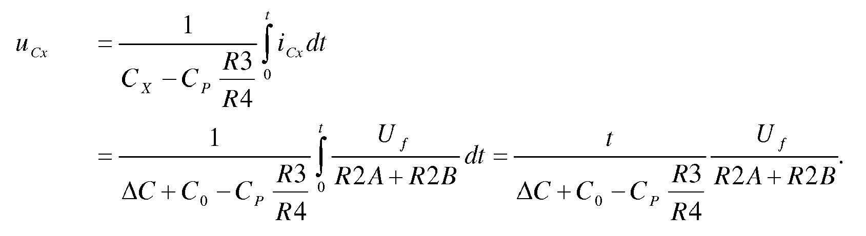
- the charging current of the measuring capacitance C X is by definition proportional to the voltage change u CX / dt.
- the voltage u CX over the quasi-stationary measuring capacitance C X thus increases in inverse proportion to the measuring capacitance C X.
- the compensation capacitance C P acts like a reduction of a constant basic component C 0 of the measuring capacitance C X (basic capacitance):
- C x C 0 + ⁇ C with C 0 > > .DELTA.C , ⁇ C hereby symbolizes the magnification of the measuring capacitance C X z to be measured.
- B due to the approach of an object to the sensor electrode SE. This reduction of the basic capacitance C 0 increases the measuring effect.
- the non-inverting amplifier I becomes, as it were, a negative capacitance of magnitude C P ⁇ R ⁇ 3 R ⁇ 4 realized that compensates for the parasitic (positive) capacitances inherent in and measured by the electronic components used. The measuring effect is thus effectively increased.
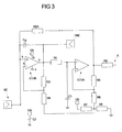
- FIG. 3 is a slightly modified embodiment of the embodiment of FIG. 2 shown, in particular instead of two resistors R2A and R2B in the feedback RK only a resistor R2A is provided. For the measurement of the frequency at the output A, an additional resistor R9 is also provided.
- the circuit construction according to the embodiment of FIG. 3 but with the circuit concept of FIG. 2 match.
- the compensation capacitance C P is in a consistent manner between the sensor electrode SE and the field beam electrode FBE are switched in such a way that they act (mathematically) like a negative capacitance and compensate parasitic capacitances during the measurement.
- a circuit layout with a single operational amplifier module is selected with the operational amplifiers IC1 / A and IC1 / B, in which the operational amplifier IC1 / B of the non-inverting amplifier I is arranged and interconnected in a special way, so that parasitic capacitances in the measurement be additionally reduced.
- the operational amplifier IC1 / B works not only with a very low input current.
- connection pin 5 On the one hand by the arrangement of the connection pin 5 at the edge of the block for the operational amplifier IC1 / B, and on the other hand due to the fact that the operational amplifier IC1 / B itself regulates a voltage difference between the positive and negative inputs to zero, parasitic capacitances are additionally avoided.
- the connection pins 5, 6, 7 and 8 for the non-inverting input, the inverting input and the output of the operational amplifier IC1 / B and for the connection to the supply voltage U B are arranged side by side and as close as possible to the sensor electrode SE, to interference or to avoid disturbing potentials.
- the connection or ground pin 4 of the operational amplifier IC1 / B is for this purpose in a preferred circuit layout spaced as far as possible to the sensor electrode SE and arranged on another side of the operational amplifier module as the connection pins 5, 6, 7 and 8.
- connection pin 5 preferably also has only short connection lines for the non-inverting (positive) input of the operational amplifier IC1 / B.
- FIG. 4 a circuit construction for a second possible embodiment of a sensor arrangement according to the invention is illustrated, in which two Sensor electrodes SE, further here represented by a single measuring capacitance C x are used in combination with a field beam electrode FBE.
- the structure of the sensor arrangement of FIG. 4 differs from the variants of the Figures 2 and 3 above all by the additional embedding of an integrator Al (also referred to as "active integrator") connected upstream of the non-inverting amplifier I.
- This additional integrator Al has, in addition to a further operational amplifier IC1 / C, an additional capacitive component C3 which is connected to the output of the operational amplifier IC1 / C of the integrator A1.
- the measuring capacitance C X and the compensation capacitance C P are respectively connected to the inverting (negative) input of the additional operational amplifier IC1 / C.
- the additional sensor electrode SE which is connected to the inverting input of the operational amplifier IC1 / C can be advantageously at least partially surrounded by another electrode, which is preferably connected to electronics ground.
- the field-beam electrode FBE can surround at least part of the first sensor electrode SE connected to the output of the operational amplifier IC1 / C.
- the electrode connected to electronic ground and the field beam electrode FBE can rotate the respective sensor electrode SE in any desired form.
- the electrode and the field beam electrode FBE the respective sensor electrode SE frame-shaped, in particular semicircular, circular or rectangular surround.
Landscapes
- Engineering & Computer Science (AREA)
- General Engineering & Computer Science (AREA)
- Theoretical Computer Science (AREA)
- Human Computer Interaction (AREA)
- Physics & Mathematics (AREA)
- General Physics & Mathematics (AREA)
- Measurement Of Resistance Or Impedance (AREA)
- Measurement Of Length, Angles, Or The Like Using Electric Or Magnetic Means (AREA)
Abstract
Die vorliegende Erfindung betrifft eine Sensoranordnung sowie ein Verfahren zur Messung einer Kapazitätsänderung an wenigstens einer Sensorelektrode gegenüber einer Grundkapazität, wobei die Grundkapazität (Co) den bei einer Messung konstanten Grundanteil einer Messkapazität (C x ) bildet und wobei - die Sensorelektrode mit einer Auswerteschaltung gekoppelt ist, die wenigstens einen Verstärker (I) und einen dem Verstärker (I) nachgeschalteten Schmitt-Trigger (ST) umfasst, und - über die Auswerteschaltung die Sensorelektrode (SE) wiederholt entladbar und aufladbar ist, so dass anhand der Frequenz, mit der das Entladen und Aufladen erfolgt, an einem dem Schmitt-Trigger (ST) nachgeschalteten Ausgang (A) auf die Größe der Messkapazität (C x ) an der Sensorelektrode (SE) geschlossen werden kann. Erfindungsgemäß liegt an einem Eingang (5) des Verstärkers (I) die Spannung über der Sensorelektrode (SE) an und an einem Ausgang (7) des Verstärkers (I) wird eine Kompensationsspannung erzeugt, wobei eine Kompensationskapazität (Cp) vordefinierter elektrischer Kapazität mit dem Ausgang (7) des Verstärkers (I) verbunden und zu dem Verstärker (I) parallel geschaltet ist, so dass die mitgemessene Grundkapazität (Co) der Sensorelektrode (SE) verringert ist, um bei der Messung parasitäre Kapazitäten zu kompensieren.The present invention relates to a sensor arrangement and to a method for measuring a change in capacitance on at least one sensor electrode relative to a basic capacitance, wherein the basic capacitance (Co) forms the basic component of a measuring capacitance (C x) which is constant during a measurement and wherein - The sensor electrode is coupled to an evaluation circuit comprising at least one amplifier (I) and the amplifier (I) downstream Schmitt trigger (ST), and - On the evaluation circuit, the sensor electrode (SE) is repeatedly dischargeable and rechargeable, so that on the Schmitt trigger (ST) downstream output (A) based on the frequency at which discharging and charging takes place on the size of the measuring capacitance (C x) can be closed at the sensor electrode (SE). According to the invention, the voltage across the sensor electrode (SE) is applied to an input (5) of the amplifier (I), and a compensation voltage is generated at an output (7) of the amplifier (I), a compensation capacitance (Cp) of predefined electrical capacitance being connected to the amplifier Output (7) of the amplifier (I) and connected in parallel with the amplifier (I), so that the measured basic capacitance (Co) of the sensor electrode (SE) is reduced to compensate for the parasitic capacitance in the measurement.
Description
Die vorliegende Erfindung betrifft eine Sensoranordnung zur Messung einer Kapazitätsänderung an wenigstens einer Sensorelektrode gemäß dem Oberbegriff des Anspruchs 1 sowie ein Verfahren zur Messung einer Kapazitätsänderung an wenigstens einer Sensorelektrode.The present invention relates to a sensor arrangement for measuring a change in capacitance on at least one sensor electrode according to the preamble of
Bei einer derartigen kapazitiv arbeitenden Sensoranordnung wird üblicherweise die sich ändernde Kapazität zwischen der Sensorelektrode und der Elektronikmasse bzw. -erde gemessen, um festzustellen, ob sich in der Umgebung der Sensorelektrode ein Objekt befindet und/oder - bei Verwendung der Sensoranordnung zur Abstandsmessung - ein Objekt der Sensorelektrode genähert hat.In such a capacitive sensor arrangement, the changing capacitance between the sensor electrode and the electronics ground or earth is usually measured to determine whether an object is located in the vicinity of the sensor electrode and / or - when using the sensor arrangement for distance measurement - an object has approached the sensor electrode.
Aus der
Bei einer Sensoranordnung zur Messung einer Kapazitätsänderung an wenigstens einer Sensorelektrode gegenüber einer Grundkapazität besteht nun grundsätzlich das Problem, dass insbesondere in der mit der Sensorelektrode gekoppelten Auswerteschaltung zahlreiche parasitäre Kapazitäten vorhanden sind, wodurch der Messeffekt reduziert wird. Dies ist insbesondere bei Anwendungen störend, bei denen die festzustellende Kapazitätsänderung vergleichsweise gering ist, z. B. im Bereich weniger pF oder sogar unter 1 pF liegt. Gerade bei einer Sensoranordnung für die Abstandsmessung zweier Komponenten in einer Werkzeugmaschine sind derartige Kapazitätsänderungen häufig entscheidend, um beispielsweise die genaue Position eines Werkzeugschlittens festzustellen.In the case of a sensor arrangement for measuring a change in capacitance on at least one sensor electrode relative to a basic capacitance, there is basically the problem that numerous parasitic capacitances are present, in particular in the evaluation circuit coupled to the sensor electrode, as a result of which the measuring effect is reduced. This is particularly troublesome in applications where the capacitance change to be detected is comparatively low, eg. B. in the range less pF or even less than 1 pF. Especially with a sensor arrangement for the distance measurement of two components in a machine tool such capacity changes are often crucial to determine, for example, the exact position of a tool slide.
Es ist daher Aufgabe der vorliegenden Erfindung, eine Sensoranordnung bereitzustellen, bei der der Messeffekt vergrößert ist und sich insbesondere kleinere Kapazitätsänderungen mit größerer Genauigkeit messen lassen.It is therefore an object of the present invention to provide a sensor arrangement in which the measuring effect is increased and in particular smaller changes in capacitance can be measured with greater accuracy.
Diese Aufgabe wird mit einer Sensoranordnung gemäß dem Anspruch 1 sowie mit dem Messverfahren des Anspruchs 15 gelöst.This object is achieved with a sensor arrangement according to
Bei dieser Sensoranordnung ist die Sensorelektrode mit einer Auswerteschaltung gekoppelt, die wenigstens einen Verstärker, z. B. einen nicht-invertierenden Operationsverstärker, und einen dem Verstärker nachgeschalteten Schmitt-Trigger umfasst. Über die Auswerteschaltung ist die Sensorelektrode wiederholt entladbar und aufladbar, so dass anhand der Frequenz, mit der das Entladen und Aufladen erfolgt, an einem dem Schmitt-Trigger nachgeschalteten Ausgang auf die Größe der Kapazität an der Sensorelektrode geschlossen werden kann. So verändert sich die Kapazität an der Sensorelektrode beispielsweise durch ein Objekt, das in ein durch die Sensorelektrode erzeugtes elektrisches Feld eindringt. Damit ändert sich die Frequenz, mit der die Ladung und Entladung der Sensorelektrode erfolgt, in charakteristischer Weise, so dass anhand der Frequenz die Größe der Kapazität an der Sensorelektrode bzw. die Änderung gegenüber der Grundkapazität bestimmt werden kann.In this sensor arrangement, the sensor electrode is coupled to an evaluation circuit, the at least one amplifier, for. B. a non-inverting operational amplifier, and comprises a Schmitt trigger downstream of the amplifier. About the evaluation circuit, the sensor electrode is repeatedly dischargeable and rechargeable, so that on the basis of the frequency with which the discharging and charging takes place at a Schmitt trigger downstream output on the size of the capacitance can be closed at the sensor electrode. For example, the capacitance on the sensor electrode changes as a result of an object penetrating into an electric field generated by the sensor electrode. Thus, the frequency with which the charge and discharge of the sensor electrode takes place, in a characteristic manner, so that the size of the capacitance at the sensor electrode or the change from the basic capacity can be determined based on the frequency.
Erfindungsgemäß ist nun weiterhin vorgesehen, dass an einem Eingang des Verstärkers die Spannung über der Sensorelektrode anliegt und an einem Ausgang des Verstärkers eine Kompensationsspannung erzeugt wird sowie eine Kompensationskapazität vordefinierter elektrischer Kapazität mit dem Ausgang des Verstärkers verbunden und zu dem Verstärker derart parallel geschaltet ist, dass sich die Grundkapazität verringert, um parasitäre Kapazitäten bei der Messung zu kompensieren. Mit anderen Worten ist eine Kompensationskapazität vordefinierter elektrischer Kapazität mit dem Ausgang des Verstärkers verbunden und zu dem Verstärker parallel geschaltet, so dass die mitgemessene Grundkapazität der Sensorelektrode - insbesondere gegenüber einer Sensoranordnung ohne Kompensationskapazität - verringert ist, um bei der Messung parasitäre Kapazitäten zu kompensieren. Durch die Kompensation der parasitären Kapazitäten mittels der Kompensationsspannung und der zusätzlichen Kompensationskapazität wird eine erhebliche Steigerung des Messeffekts und damit der Sensorempfindlichkeit erreicht.According to the invention, it is further provided that at an input of the amplifier, the voltage is applied across the sensor electrode and at an output of the amplifier, a compensation voltage is generated and a compensation capacity pre-defined electrical capacitance is connected to the output of the amplifier and connected in parallel to the amplifier such that the basic capacitance decreases to compensate for parasitic capacitance in the measurement. In other words, a compensation capacitance of predefined electrical capacitance is connected to the output of the amplifier and connected in parallel to the amplifier so that the measured basic capacitance of the sensor electrode-in particular with respect to a sensor arrangement without compensation capacitance-is reduced in order to compensate parasitic capacitances during the measurement. By compensating the parasitic capacitances by means of the compensation voltage and the additional compensation capacitance, a considerable increase of the measuring effect and thus of the sensor sensitivity is achieved.
Durch die erfindungsgemäße Lösung kann ein Abgleich der Sensoranordnung bei oder nach der Montage weitestgehend oder - je nach Schaltungslayout - auch vollständig vermieden werden. Ferner kann eine erfindungsgemäße Sensoranordnung vergleichsweise einfach auch in kleinsten Bauformen und mit wenigen (diskreten) Bauteilen ausgeführt werden, ohne dass diese unmittelbar zu einer erheblichen Verkleinerung der Schaltabstände führt. So hat sich gezeigt, dass grundsätzlich mit einer erfindungsgemäßen Sensoranordnung teilweise deutlich größere Schaltabstände realisierbar sind als bei vergleichbaren Sensoranordnungen ohne Kompensationskapazität.Due to the solution according to the invention, a balance of the sensor arrangement during or after assembly as far as possible or - depending on the circuit layout - also completely avoided. Furthermore, a sensor arrangement according to the invention can be carried out comparatively easily even in the smallest designs and with few (discrete) components, without these directly leading to a considerable reduction of the switching distances. It has thus been shown that, in principle, significantly greater switching distances can be achieved with a sensor arrangement according to the invention than with comparable sensor arrangements without compensation capacity.
Die Kompensationskapazität kann grundsätzlich über ein geschickt gewähltes Schaltungslayout in die Schaltungsanordnung eingebracht sein, so dass ohnehin vorzusehende und bei der Messung kapazitiv wirkende Schaltungsteile (z.B. Leitungen) als eine Kompensationskapazität fungieren, mit der eine gemessene Grundkapazität der Sensorelektrode verringert wird. Darüber hinaus kann eine Kompensationskapazität über wenigstens ein separates bzw. diskretes vorzugsweise kapazitives Bauelement, z.B. in Form eines Kondensators, bereitgestellt sein, dass zur Kompensation parasitärer Kapazitäten gezielt auf die erfindungsgemäße Art und Weise in der Schaltungsanordnung angeordnet wurde. Eine Kompensationskapazität kann somit insbesondere durch ein diskretes elektrisches Bauelement oder mehrere diskrete elektrischen Bauelemente in der Sensoranordnung bzw. einer zugehörigen Schaltung bereitgestellt sein.The compensation capacitance may in principle be introduced into the circuit arrangement via a cleverly selected circuit layout, so that circuit components (for example lines) which are to be provided anyway and are capacitive in the measurement function as a compensation capacitance with which a measured basic capacitance of the sensor electrode is reduced. In addition, a compensation capacitance may be provided via at least one discrete, preferably capacitive device, e.g. in the form of a capacitor, be provided that was specifically designed to compensate for parasitic capacitances in the manner according to the invention in the circuit arrangement. A compensation capacitance can thus be provided in particular by a discrete electrical component or a plurality of discrete electrical components in the sensor arrangement or an associated circuit.
In einer bevorzugten Ausführungsvariante ist zusätzlich zu der wenigstens einen Sensorelektrode eine Feldbündelelektrode vorgesehen, die derart ausgebildet und geschaltet ist, dass ein von der Feldbündelelektrode erzeugtes elektrisches Feld eine räumliche Verteilung eines von der Sensorelektrode erzeugten elektrischen Feldes derart beeinflusst, dass das Feld der Sensorelektrode in einem räumlichen Messbereich gebündelt ist. Eine derartige Feldbündelelektrode kann beispielsweise mindestens eine Sensorelektrode teilweise oder vollständig umlaufend umgeben, so dass eine Bündelung des von der Sensorelektrode erzeugten elektrischen Felds in dem von der Feldbündelelektrode umgebenden Bereich erreicht wird.In a preferred embodiment, in addition to the at least one sensor electrode, a field beam electrode is provided, which is designed and in that an electric field generated by the field beam electrode influences a spatial distribution of an electric field generated by the sensor electrode such that the field of the sensor electrode is bundled in a spatial measuring range. Such a field beam electrode can surround, for example, at least one sensor electrode partially or completely circumferentially, so that a bundling of the electric field generated by the sensor electrode is achieved in the area surrounding the field beam electrode.
In einer als besonders vorteilhaft erachteten Ausführungsvariante einer erfindungsgemäßen Sensoranordnung mit einer Feldbündelelektrode ist die Feldbündelelektrode mit dem Ausgang des Verstärkers verbunden und die Feldbündelelektrode liegt damit auf dem Potential der Kompensationsspannung. Hierbei ist dann die zur Kompensation parasitärer Kapazitäten vorgesehene zusätzliche Kompensationskapazität zwischen die Feldbündelelektrode und die Sensorelektrode geschaltet. Indem die zur Kompensation parasitärer Kapazitäten vorgesehene und ausgebildete Kompensationskapazität zwischen den auf unterschiedlichen Potentialen liegenden Elektroden angeordnet ist, wird eine besonders effektiv arbeitende Sensoranordnung erzielt, die eine zusätzliche Feldbündelelektrode aufweist und bei der der Messeffekt gegenüber bekannten Sensoranordnungen deutlich verbessert ist.In a variant embodiment of a sensor arrangement according to the invention comprising a field beam electrode, the field beam electrode is connected to the output of the amplifier and the field beam electrode is thus at the potential of the compensation voltage. In this case, the additional compensation capacitance provided for compensating parasitic capacitances is connected between the field-beam electrode and the sensor electrode. By arranging the compensating capacitance provided and designed for compensating parasitic capacitances between the electrodes located at different potentials, a particularly effectively operating sensor arrangement is achieved which has an additional field-beam electrode and in which the measuring effect is significantly improved compared to known sensor arrangements.
Zur Unterdrückung hochfrequenter Störungen bei der Messung mit Hilfe der Sensoranordnung wird es ferner bevorzugt, dass zwischen dem Verstärker und dem Schmitt-Trigger ein Tiefpass geschaltet ist. Zur Unterdrückung hochfrequenter Störungen kann es zudem vorteilhaft sein, zwischen der Sensorelektrode und dem Verstärker eine Induktivität vorzusehen.To suppress high-frequency interference in the measurement by means of the sensor arrangement, it is further preferred that a low-pass filter is connected between the amplifier and the Schmitt trigger. To suppress high-frequency interference, it may also be advantageous to provide an inductance between the sensor electrode and the amplifier.
In einer bevorzugten Ausführungsvariante ist die Auswerteschaltung ferner dazu ausgebildet und vorgesehen, mit einer einzelnen asymmetrischen Versorgungsspannung betrieben zu werden. Hierzu werden beispielsweise die Fußpunkte des Schmitt-Triggers und eines nicht-invertierenden Verstärkers über einen Spannungsteiler aus zwei gleichgroßen, relativ niederohmigen Widerständen zwischen der Versorgungsspannung und Masse angeschlossen.In a preferred embodiment, the evaluation circuit is further designed and intended to be operated with a single asymmetrical supply voltage. For this purpose, for example, the bases of the Schmitt trigger and a non-inverting amplifier are connected via a voltage divider of two equal, relatively low-resistance resistors between the supply voltage and ground.
In einer möglichen Weiterbildung einer erfindungsgemäßen Sensoranordnung weist diese eine zweite Sensorelektrode und/oder vorteilhaft einem dem Verstärker vorgeschalteten aktiven Integrierer auf. Beide Sensorelektroden bilden eine Gegenkopplungskapazität des Integrieres. Eine Feldbündelelektrode kann auch hier optional zwischen dem - vorzugsweise nicht-invertierenden - Verstärker und der zur Kompensation parasitärer Kapazitäten vorgesehenen Kompensationskapazität angeordnet werden.In one possible development of a sensor arrangement according to the invention, the latter has a second sensor electrode and / or advantageously an active integrator connected upstream of the amplifier. Both sensor electrodes form a negative feedback capacity of the integrator. A field beam electrode can also be here optionally between the - preferably non-inverting - amplifier and provided for compensating parasitic capacitance compensation capacity can be arranged.
In einer Ausführungsform der vorliegenden Erfindung ist die komplette Auswerteschaltung, insbesondere mit (nicht-invertierendem) Verstärker und Schmitt-Trigger, auf einer Leiterplatte untergebracht.In one embodiment of the present invention, the complete evaluation circuit, in particular with (non-inverting) amplifier and Schmitt trigger, is accommodated on a printed circuit board.
Hier kann eine weitere Reduzierung parasitärer Kapazitäten erreicht werden, indem eine in dieser Hinsicht optimierte Schaltungs- und Layout-Gestaltung verwendet ist. In diesem Zusammenhang hat sich beispielsweise eine Sensoranordnung als besonders vorteilhaft herausgestellt, bei der
- der der Sensorelektrode nachgeschaltete Operationsverstärker mehrere an der Leiterplatte nebeneinander liegende Anschlusspins aufweist,
- die Sensorelektrode mit dem nicht-invertierenden Eingang des Operationsverstärkers über einen Anschlusspin des Operationsverstärkers verbunden ist und
- dieser Anschlusspin zum einen den äußersten Anschlusspin der nebeneinander liegenden Anschlusspins bildet und dieser mit der Sensorelektrode verbundene Anschlusspin zum anderen unmittelbar neben dem Anschlusspin für den invertierenden Eingang des Operationsverstärkers liegt.
- the operational amplifier connected downstream of the sensor electrode has a plurality of connection pins arranged next to one another on the printed circuit board,
- the sensor electrode is connected to the non-inverting input of the operational amplifier via a terminal pin of the operational amplifier and
- this connection pin on the one hand forms the outermost connection pin of the adjoining connection pins and this connection pin connected to the sensor electrode lies to the other directly next to the connection pin for the inverting input of the operational amplifier.
Indem damit kein weiterer Anschlusspin zwischen dem mit der Sensorelektrode verbundenen äußersten Anschlusspin für den nicht-invertierenden (positiven) Eingang des Operationsverstärkers und dem Anschlusspin für den invertierenden (negativen) Eingang desselben Operationsverstärkers liegt, können parasitäre Kapazitäten zusätzlich reduziert werden. So regelt der Operationsverstärker von sich aus eine Spannungsdifferenz zwischen den beiden Eingängen (+ und -) zu Null, so dass durch den Anschlusspin für den invertierenden Eingang keine größeren parasitären Kapazitäten bei der Messung hervorgerufen werden.By thus no further connection pin between the sensor connected to the outer terminal pin for the non-inverting (positive) input of the operational amplifier and the terminal pin for the inverting (negative) input of the same operational amplifier, parasitic capacitances can be additionally reduced. Thus, the operational amplifier of itself regulates a voltage difference between the two inputs (+ and -) to zero, so that caused by the connection pin for the inverting input no larger parasitic capacitance in the measurement.
In bevorzugten Ausführungsvarianten ist die Sensoranordnung dazu ausgebildet und vorgesehen, durch eine sich ändernde Kapazität an der Sensorelektrode zu bestimmen, ob sich ein Objekt der Sensorelektrode genähert hat und/oder sich ein Objekt in einem Umgebungsbereich um die Sensorelektrode befindet. Derart kann eine erfindungsgemäße Sensoranordnung in einem Näherungsschalter oder -sensor Anwendung finden.In preferred embodiments, the sensor arrangement is designed and provided to determine, by means of a changing capacitance at the sensor electrode, whether an object has approached the sensor electrode and / or an object is located in a surrounding area around the sensor electrode. In this way, a sensor arrangement according to the invention can be used in a proximity switch or sensor.
Eine bevorzugte Anwendung sieht vor, dass durch eine sich ändernde Kapazität an der Sensorelektrode ein Abstand zwischen zwei Komponenten einer Werkzeugmaschine bestimmt wird. Derart kann eine erfindungsgemäße Sensoranordnung die Automation bei Werkzeugmaschinen und bei Maschinen im Allgemeinen erheblich vereinfachen und einen automatisierten Betrieb von Maschinen verbessern, bei denen die Durchführung aufeinanderfolgender Prozessschritte von einer bestimmten Lage bzw. Position zweier Komponenten zueinander abhängt und diese sensorisch zu erfassen ist. Durch die Verbesserung des Messeffekts aufgrund der gezielten, wenigstens teilweisen Kompensation parasitärer Kapazitäten in der Auswerteschaltung kann die entsprechende Lage bzw. Position genauer und folglich mit geringerer Fehlertoleranz bestimmt werden.A preferred application provides that a distance between two components of a machine tool is determined by a changing capacitance on the sensor electrode. In this way, a sensor arrangement according to the invention can greatly simplify the automation of machine tools and machines in general and improve an automated operation of machines in which the execution of successive process steps depends on a specific position or position of two components and this is to be detected by sensors. By improving the measurement effect due to the targeted, at least partial compensation of parasitic capacitances in the evaluation circuit, the corresponding position or position can be determined more accurately and consequently with a lower fault tolerance.
Darüber hinaus ist beispielsweise auch eine Anwendung in einem Füllstandsensor denkbar, um mittels der Sensorelektrode den Füllstand einer Flüssigkeit in einem Behälter kapazitiv zu bestimmen.In addition, for example, an application in a level sensor is conceivable to capacitively determine the level of a liquid in a container by means of the sensor electrode.
Ein weiterer Aspekt der vorliegenden Erfindung ist ein Verfahren zur Messung einer Kapazitätsänderung an wenigstens einer Sensorelektrode mit einer Grundkapazität gemäß dem Anspruch 15.Another aspect of the present invention is a method for measuring a capacitance change on at least one sensor electrode with a basic capacitance according to claim 15.
Hierbei ist vorgesehen, dass
- die Sensorelektrode mit einer Auswerteschaltung gekoppelt ist, die wenigstens einen Verstärker und einen dem Verstärker nachgeschalteten Schmitt-Trigger umfasst,
- über die Auswerteschaltung die Sensorelektrode wiederholt entladen und aufgeladen wird, so dass anhand der Frequenz, mit der das Entladen und Aufladen erfolgt, an einem dem Schmitt-Trigger nachgeschalteten Ausgang auf die Größe der Kapazität an der Sensorelektrode geschlossen werden kann,
- die Spannung über der Sensorelektrode an einen Eingang des Verstärkers angelegt wird und eine Kompensationsspannung an einem Ausgang des Verstärkers erzeugt wird, und
- eine Kompensationskapazität vordefinierter elektrischer Kapazität vorgesehen wird, die mit dem Ausgang des Verstärkers verbunden und zu dem Verstärker derart parallel geschaltet ist, dass sich die Grundkapazität der Sensorelektrode verringert, um bei der Messung parasitäre Kapazitäten zu kompensieren.
- the sensor electrode is coupled to an evaluation circuit comprising at least one amplifier and a Schmitt trigger connected downstream of the amplifier,
- the sensor electrode is repeatedly discharged and charged via the evaluation circuit so that, based on the frequency with which the discharging and charging takes place, the magnitude of the capacitance on the sensor electrode can be deduced at an output downstream of the Schmitt trigger,
- the voltage across the sensor electrode is applied to an input of the amplifier and a compensation voltage is generated at an output of the amplifier, and
- a compensation capacity of predefined electrical capacitance is provided which is connected to the output of the amplifier and to the amplifier is connected in parallel so that the basic capacitance of the sensor electrode is reduced in order to compensate for parasitic capacitance during the measurement.
In Übereinstimmung zu einer erfindungsgemäßen Sensoranordnung zeichnet sich ein erfindungsgemäßes Verfahren somit maßgeblich durch das Vorsehen einer Kompensationskapazität aus, die die mit dem Ausgang des Verstärkers verbunden und zu diesem parallel geschaltet ist. Die zuvor und nachfolgend für Ausführungsbeispiele einer erfindungsgemäßen Sensoranordnung erläuterten Merkmale gelten somit auch für die entsprechenden Varianten eines erfindungsgemäßen Messverfahrens und umgekehrt.In accordance with a sensor arrangement according to the invention, a method according to the invention is thus significantly characterized by the provision of a compensation capacitance which is connected to the output of the amplifier and connected in parallel thereto. The features explained above and below for exemplary embodiments of a sensor arrangement according to the invention thus also apply to the corresponding variants of a measuring method according to the invention and vice versa.
Weitere Vorteile und Merkmale der vorliegenden Erfindung werden bei der nachfolgenden Beschreibung von Ausführungsbeispielen anhand der Figuren deutlich werden.Further advantages and features of the present invention will become apparent in the following description of exemplary embodiments with reference to the figures.
Es zeigen:
- Fig. 1
- schematisch ein grundlegendes Schaltungskonzept für eine erfindungsgemäße Sensoranordnung;
- Fig. 2
- das Schaltbild für eine erste Ausführungsvariante einer erfindungsgemäßen Sensoranordnung mit einer Sensorelektrode und einer Feldbündelelektrode;
- Fig. 3
- ein Schaltbild zu einer Weiterbildung der Ausführungsvariante der
Figur 2 ; - Fig. 4
- ein Schaltbild zu einer zweiten Ausführungsvariante einer erfindungsgemäßen Sensoranordnung mit zwei Sensorelektroden.
- Fig. 1
- schematically a basic circuit concept for a sensor arrangement according to the invention;
- Fig. 2
- the circuit diagram for a first embodiment of a sensor arrangement according to the invention with a sensor electrode and a field beam electrode;
- Fig. 3
- a diagram of a development of the embodiment of the
FIG. 2 ; - Fig. 4
- a circuit diagram of a second embodiment of a sensor arrangement according to the invention with two sensor electrodes.
Die
Die Messkapazität Cx wird beispielsweise über einen Rückkopplungswiderstand mit einem Wechselstrom als getakteten Gleichstrom beaufschlagt. An einem, dem Schmitt-Trigger ST nachgeschalteten Ausgang A ist dann anhand eines Mess(spannungs)Signals Uf eine Frequenz messbar, die von der Größe der Messkapazität CX abhängt. Ändert sich die Größe der Messkapazität CX beispielsweise durch ein in der Nähe der Sensorelektrode befindliches Objekt, verändert sich (proportional hierzu) die Frequenz zwischen Entladen und Aufladen der Messkapazität CX. Folglich kann über die sich an dem Ausgang A einstellende Frequenz des Messsignals Uf auf die momentane Größe der Messkapazität CX geschlossen werden bzw. die Messkapazität Cx bestimmt werden.The measuring capacitance Cx is supplied, for example, via a feedback resistor with an alternating current as a clocked direct current. At a downstream of the Schmitt trigger ST output A is then based on a measurement (voltage) signal U f a frequency measurable, which depends on the size of the measuring capacitance C X. If the size of the measuring capacitance C X changes, for example, due to an object located in the vicinity of the sensor electrode, the frequency changes (proportionally) between discharging and charging the measuring capacitance C X. Consequently, it is possible to determine the instantaneous magnitude of the measuring capacitance C X via the frequency of the measuring signal U f at the output A, or to determine the measuring capacitance C x .
Die dargestellte Sensoranordnung ist vorzugsweise für einen Abstandssensor oder einen Näherungsschalter vorgesehen, beispielsweise für die Automatisierung von Verstellprozessen bei (Werkzeug-)Maschinen. Hierbei ist üblicherweise die zu messende Änderung der Messkapazität Cx gegenüber einer Grundkapazität vergleichsweise gering, wobei hierbei als Grundkapazität die Kapazität der unbeeinflussten Sensorelektrode, d. h. die bei einer Kalibrierung der Sensoranordnung gemessene Größe der Messkapazität Cx, verstanden wird. Typischerweise liegt die zu erfassende und auszuwertende Änderung der Messkapazität CX im Bereich weniger pF (≤ 10 pF) oder sogar unter 1 pF. Insbesondere bei einer derartigen Konstellation sind die über die Auswerteschaltung eingebrachten und mit gemessenen parasitären Kapazitäten sehr störend und beeinflussen den Messeffekt teilweise gravierend.The illustrated sensor arrangement is preferably provided for a distance sensor or a proximity switch, for example for the automation of adjustment processes in (tool) machines. In this case, the change of the measuring capacitance Cx to be measured compared to a basic capacitance is usually comparatively small, the basic capacitance being understood to be the capacitance of the non-influenced sensor electrode, ie the size of the measuring capacitance Cx measured during a calibration of the sensor arrangement. Typically, the change in the measuring capacitance C X to be detected and evaluated lies in the range of less pF (≦ 10 pF) or even less than 1 pF. Especially in such a constellation, the introduced via the evaluation circuit and with measured parasitic capacitances are very disturbing and affect the measurement effect sometimes serious.
Bei einer erfindungsgemäßen Lösung gemäß der
Alternativ oder ergänzend zu einem separaten kapazitivem Bauelement zur Bereitstellung der Kompensationskapazität CP kann die Kompensationskapazität CP über ein geschickt gewähltes Schaltungslayout in die Schaltungsanordnung eingebracht sein, so dass ohnehin vorzusehende und bei der Messung kapazitiv wirkende Schaltungsteile (z.B. Leitungen) als eine Kompensationskapazität CP fungieren, mit der die gemessene Grundkapazität der Sensorelektrode SE verringert wird.Alternatively, or in addition to a separate capacitive component for providing the compensation capacitance C P is the compensation capacitance C P can a cleverly chosen circuit layout be introduced into the circuit arrangement, so that anyway to be provided and capacitively acting in the measurement circuit parts (eg lines) act as a compensation capacitance C P , with the measured basic capacitance of the sensor electrode SE is reduced.
Die
Der nicht-invertierende Verstärker I weist in bekannter Art und Weise neben dem Operationsverstärker IC1/B zwei Widerstände R3 und R4 zur Bildung eines Spannungsteilers auf. Der Operationsverstärker IC1/B des Verstärkers I weist fünf Anschlusspins 4, 5, 6, 7 und 8 auf, wobei der Anschlusspin 5 dem nicht-invertierenden (positiven) Eingang des Operationsverstärkers IC1/B und der Anschlusspin 6 dem invertierenden (negativen) Eingang zugeordnet sind. Der Anschlusspin 4 stellt den Massepin dar und an dem Anschlusspin 8 liegt eine Versorgungsspannung UB an. Der Anschlusspin 7 wiederum stellt den Ausgang des Operationsverstärkers IC1/B dar. Mittels des Operationsverstärkers IC1/B erzeugt der Verstärker I an seinem durch den Anschlusspin 7 gekennzeichneten Ausgang eine definierte Kompensationsspannung, die proportional zu der Spannung über der Sensorelektrode SE bzw. über der Messkapazität Cx ist und die (um einen vorgegebenen Verstärkungsfaktor) gegenüber dieser Spannung erhöht ist.The non-inverting amplifier I has in a known manner, in addition to the operational amplifier IC1 / B, two resistors R3 and R4 to form a voltage divider. The operational amplifier IC1 / B of the amplifier I has five
Der Schmitt-Trigger ST weist neben dem Operationsverstärker IC1/A noch zusätzliche Widerstände R5 und R6 auf und ist in an sich bekannter Bauweise ausgebildet. Der Operationsverstärker IC1/A weist insbesondere an einem Anschlusspin 2 den invertierenden Eingang auf, der mit dem Tiefpass TP und hierüber mit dem Ausgang des Operationsverstärkers IC1/B des Verstärkers I verbunden ist. Dem nicht-invertierenden (positiven) Eingang des Operationsverstärkers IC1/A ist ein Anschlusspin 3 zugeordnet, an den das Ausgangssignal des Operationsverstärkers IC1/A zurückgeführt ist. Den Ausgang des Operationsverstärkers IC1/A definiert ein weiterer Anschlusspin 1.The Schmitt trigger ST has, in addition to the operational amplifier IC1 / A, additional resistors R5 and R6 and is constructed in a manner known per se. The operational amplifier IC1 / A has, in particular at a connection pin 2, the inverting input, which is connected to the low-pass filter TP and via this to the output of the operational amplifier IC1 / B of the amplifier I. The non-inverting (positive) input of the operational amplifier IC1 / A is assigned a terminal pin 3, to which the output signal of the operational amplifier IC1 / A is fed back. The output of the operational amplifier IC1 / A defines another terminal pin. 1
Der Ausgang des Schmitt-Triggers ST ist über eine Rückkopplung RK - hier aufweisend zwei Widerstände R2A und R2B - mit dem Eingang des Operationsverstärkers IC1/B (am Anschlusspin 5) verbunden. An einem Knoten K der gezeigten Schaltung sind die Rückkopplung RK, der nicht-invertierende Eingang des Operationsverstärkers IC1/B, eine Sensorelektrode SE mit der Messkapazität CX und eine zu der Kompensationskapazität CP führende Anschlussleitung miteinander verbunden. Eine zweite zu der Kompensationskapazität CP führende Anschlussleitung ist dementsprechend zwischen dem Ausgang des Verstärkers I bzw. dem Ausgang des zugehörigen Operationsverstärkers IC1/B und dem Tiefpass TP angeschlossen.The output of the Schmitt trigger ST is via a feedback RK - here having two resistors R2A and R2B - with the input of the operational amplifier IC1 / B (am Connection pin 5) connected. At a node K of the circuit shown, the feedback RK, the non-inverting input of the operational amplifier IC1 / B, a sensor electrode SE with the measuring capacitance C X and a connecting line leading to the compensation capacitance C P are interconnected. A second connecting line leading to the compensation capacitance C P is accordingly connected between the output of the amplifier I or the output of the associated operational amplifier IC1 / B and the low-pass filter TP.
Die Kompensationskapazität CP ist ferner (in Form eines Kondensators) zwischen die Sensorelektrode SE und eine Feldbündelelektrode FBE geschaltet. Die Feldbündelelektrode FBE bündelt dabei, wie z. B. aus der
Ein ebenfalls der Unterdrückung hochfrequenter Störungen dienendes, induktives Bauelement L der Sensorelektrode SE sowie zusätzliche Widerstände R7 und R8 bei dem Verstärker I und dem Schmitt-Trigger ST komplettieren die analoge Sensorelektronik der gezeigten Schaltung.An inductive component L of the sensor electrode SE, which also serves to suppress high-frequency interference, and additional resistors R7 and R8 in the amplifier I and the Schmitt trigger ST complete the analog sensor electronics of the circuit shown.
Wie aus der
Die Wirkung der Kompensationskapazität CP wird nachfolgend näher veranschaulicht werden.The effect of the compensation capacity C P will be illustrated in more detail below.
Eine Spannung uCX über der Messkapazität CX baut sich mit einem Ladestrom 

auf.A voltage u CX above the measuring capacitance C X builds up with a charging current
on.
Der Ladestrom der Messkapazität CX ist definitionsgemäß proportional zur Spannungsänderung uCX/dt.The charging current of the measuring capacitance C X is by definition proportional to the voltage change u CX / dt.
Die Spannung uCX über der quasi stationären Messkapazität CX steigt somit umgekehrt proportional zu der Messkapazität CX. Über die Kompensationsspannung des nicht-invertierenden Verstärkers I und die Kompensationskapazität CP (zwischen dem Ausgang des nicht-invertierenden Verstärkers I und der Leitung der Sensorelektrode SE und der Senorelektrode SE selbst) fließt ein weiterer, zur Spannungsänderung duCp/dt proportionaler Kompensationsstrom 
in den Knoten K an der Messkapazität CX, der die Spannung uCx schneller ansteigen lässt (wie bei einer Verkleinerung der Messkapazität CX): 
in the node K at the measuring capacitance C X , which causes the voltage u Cx to increase more rapidly (as in the case of a reduction of the measuring capacitance C X ):
Beide Effekte überlagern sich. In Verbindung mit dem Kompensationsstrom aus dem nicht-invertierenden Verstärker I wirkt die Kompensationskapazität CP wie eine Reduktion eines konstanten Grundanteils C0 der Messkapazität CX (Grundkapazität): ![]()
Δ C symbolisiert hierbei die zu messende Vergrößerung der Messkapazität CX z. B. aufgrund der Annäherung eines Objekts an die Sensorelektrode SE. Durch diese Reduktion der Grundkapazität C0 wird der Messeffekt erhöht.Both effects are superimposed. In conjunction with the compensation current from the non-inverting amplifier I, the compensation capacitance C P acts like a reduction of a constant basic component C 0 of the measuring capacitance C X (basic capacitance): ![]()
Δ C hereby symbolizes the magnification of the measuring capacitance C X z to be measured. B. due to the approach of an object to the sensor electrode SE. This reduction of the basic capacitance C 0 increases the measuring effect.
Die über die Kompensationskapazität CP abfallende Spannung uCp ist die Differenz der Kompensationsspannung, also der Ausgangsspannung des nicht-invertierenden Verstärkers und der Spannung über der Messkapazität Cx: ![]()
wobei v den Verstärkungsfaktor des nicht-invertierenden Verstärkers I mit ![]()
![]()
where v is the gain of the non-inverting amplifier I with ![]()
Somit wird 

Mit dem Gesamtstrom in die Messkapazität CX ![]()
![]()
Über den nicht-invertierenden Verstärker I wird somit mit Hilfe der Kompensationskapazität CP (und gegebenenfalls einem weiteren hierzu parallel liegenden Kondensator) quasi eine negative Kapazität der Größe ![]()
![]()
In der
Im vorliegenden Fall ist ein Schaltungslayout mit einem einzelnen Operationsverstärkerbaustein mit den Operationsverstärkern IC1/A und IC1/B gewählt, bei dem der Operationsverstärker IC1/B des nicht-invertierenden Verstärkers I in besonderer Weise angeordnet und verschaltet ist, so dass parasitäre Kapazitäten bei der Messung zusätzlich reduziert werden. Hierzu arbeitet der Operationsverstärker IC1/B nicht nur mit einem sehr geringen Eingangsstrom. Vielmehr ist zusätzlich noch vorgesehen, dass der Anschlusspin 5 für den nicht-invertierenden (positiven) Eingang des Operationsverstärkers IC1/B den äußersten von vier nebeneinander liegenden (Eingangs-)Anschlusspins 5, 6, 7, 8 darstellt und der Anschlusspin 5 ausschließlich in unmittelbarer Nachbarschaft zu dem Anschlusspin 6 für den invertierenden (negativen) Eingang des Operationsverstärkers IC1/B liegt. Zwischen den beiden Anschlusspins 5 und 6 ist dementsprechend kein weiterer Anschlusspin des Operationsverstärkers IC1/B vorgesehen.In the present case, a circuit layout with a single operational amplifier module is selected with the operational amplifiers IC1 / A and IC1 / B, in which the operational amplifier IC1 / B of the non-inverting amplifier I is arranged and interconnected in a special way, so that parasitic capacitances in the measurement be additionally reduced. For this purpose, the operational amplifier IC1 / B works not only with a very low input current. Rather, it is additionally provided that the
Einerseits durch die Anordnung des Anschlusspins 5 am Rand des Bausteins für den Operationsverstärker IC1/B und andererseits aufgrund der Tatsache, dass der Operationsverstärker IC1/B von sich aus eine Spannungsdifferenz zwischen den positiven und negativen Eingängen zu Null regelt, werden parasitäre Kapazitäten zusätzlich vermieden. Die Anschlusspins 5, 6, 7 und 8 für den nicht-invertierenden Eingang, den invertierenden Eingang und den Ausgang des Operationsverstärkers IC1/B und für den Anschluss an die Versorgungsspannung UB sind nebeneinander angeordnet und möglichst nahe an der Sensorelektrode SE, um Störeinflüsse bzw. störende Potentiale zu vermeiden. Der Anschluss- bzw. Massepin 4 des Operationsverstärkers IC1/B ist zu eben diesem Zweck bei einem bevorzugten Schaltungslayout möglichst weit zu der Sensorelektrode SE beabstandet und auf einer anderen Seite des Operationsverstärkerbausteins angeordnet als die Anschlusspins 5, 6, 7 und 8.On the one hand by the arrangement of the
Darüber hinaus besitzt der Anschlusspin 5 für den nicht-invertierenden (positiven) Eingang des Operationsverstärkers IC1/B vorzugsweise auch nur kurze Anschlussleitungen.In addition, the
Mit der
Der Aufbau der Sensoranordnung der
Die auf den invertierenden Eingang des Operationsverstärkers IC1/C geschaltete zusätzliche Sensorelektrode SE kann vorteilhaft zumindest teilweise von einer weiteren, vorzugsweise auf Elektronikmasse geschalteten Elektrode umgeben sein. Des Weiteren kann die Feldbündelelektrode FBE zumindest einen Teil der ersten, am Ausgang des Operationsverstärkers IC1/C angeschlossenen Sensorelektrode SE umgeben. Dabei können die auf Elektronikmasse geschaltete Elektrode und die Feldbündelelektrode FBE die jeweilige Sensorelektrode SE in beliebiger Form umlaufen. Beispielsweise können die Elektrode und die Feldbündelelektrode FBE die jeweilige Sensorelektrode SE rahmenförmig, insbesondere halbkreisförmig, kreisförmig oder rechteckförmig umgeben.The additional sensor electrode SE which is connected to the inverting input of the operational amplifier IC1 / C can be advantageously at least partially surrounded by another electrode, which is preferably connected to electronics ground. Furthermore, the field-beam electrode FBE can surround at least part of the first sensor electrode SE connected to the output of the operational amplifier IC1 / C. In this case, the electrode connected to electronic ground and the field beam electrode FBE can rotate the respective sensor electrode SE in any desired form. For example, the electrode and the field beam electrode FBE the respective sensor electrode SE frame-shaped, in particular semicircular, circular or rectangular surround.
- 1 - 81 - 8
- Anschlusspinconnector pin
- AA
- Ausgangoutput
- Alal
- Aktiver IntegratorActive integrator
- CoCo
- Grundkapazität der Messkapazität Cx Basic capacity of the measuring capacity C x
- C1, C2, C3C1, C2, C3
- Kapazitives BauelementCapacitive component
- Cp C p
- Kompensationskapazitätcompensation capacitor
- Cx C x
- Messkapazitätmeasuring capacitance
- II
- Verstärkeramplifier
- IC1/A, IC1/B, IC1/CIC1 / A, IC1 / B, IC1 / C
- Operationsverstärkeroperational amplifiers
- FBEFBE
- FeldbündelelektrodeField confining electrode
- KK
- Knotennode
- LL
- Induktives BauelementInductive component
- R1, R2A, R2B, R3 - R9R1, R2A, R2B, R3 - R9
- Widerstandresistance
- RKRK
- Rückkopplungfeedback
- SESE
- Sensorelektrodesensor electrode
- STST
- Schmitt-TriggerSchmitt trigger
- TPTP
- Tiefpasslowpass
- UB U B
- Versorgungsspannungsupply voltage
- Uf U f
- Messsignalmeasuring signal
Claims (15)
an einem Eingang (5) des Verstärkers (I) die Spannung über der Sensorelektrode (SE) anliegt und an einem Ausgang (7) des Verstärkers (I) eine Kompensationsspannung erzeugt wird, und dass eine Kompensationskapazität (Cp) vordefinierter elektrischer Kapazität mit dem Ausgang (7) des Verstärkers (I) verbunden und zu dem Verstärker (I) parallel geschaltet ist, so dass die mitgemessene Grundkapazität (Co) der Sensorelektrode (SE) verringert ist, um bei der Messung parasitäre Kapazitäten zu kompensieren.Sensor arrangement for measuring a change in capacitance on at least one sensor electrode with a basic capacitance, wherein the basic capacitance (C 0 ) forms the basic component of a measuring capacitance (C x ) that is constant during a measurement, and wherein
at an input (5) of the amplifier (I), the voltage across the sensor electrode (SE) is applied and at an output (7) of the amplifier (I) a compensation voltage is generated, and that a compensation capacity (Cp) predefined electrical capacity with the output (7) of the amplifier (I) and connected in parallel with the amplifier (I), so that the measured basic capacitance (Co) of the sensor electrode (SE) is reduced in order to compensate parasitic capacitances during the measurement.
die Spannung über der Sensorelektrode (SE) an einen Eingang (5) des Verstärkers (I) angelegt wird und eine Kompensationsspannung an einem Ausgang (7) des Verstärkers (I) erzeugt wird, und dass eine Kompensationskapazität (Cp) vordefinierter elektrischer Kapazität vorgesehen wird, die mit dem Ausgang (7) des Verstärkers (I) verbunden und zu dem Verstärker (I) parallel geschaltet ist, so dass sich die mitgemessene Grundkapazität (Co) der Sensorelektrode (SE) verringert ist, um bei der Messung parasitäre Kapazitäten zu kompensieren.Method for measuring a change in capacitance on at least one sensor electrode with a basic capacitance, wherein the basic capacitance (C 0 ) forms the basic component of a measuring capacitance (C x ) which is constant during a measurement, and wherein
the voltage across the sensor electrode (SE) is applied to an input (5) of the amplifier (I) and a compensation voltage is applied to an output (7) of the amplifier Amplifier (I) is generated, and that a compensation capacity (Cp) of predefined electrical capacitance is provided, which is connected to the output (7) of the amplifier (I) and connected in parallel to the amplifier (I), so that the measured basic capacity (Co) of the sensor electrode (SE) is reduced in order to compensate for parasitic capacitance during the measurement.
Applications Claiming Priority (1)
| Application Number | Priority Date | Filing Date | Title |
|---|---|---|---|
| DE102013201704.9A DE102013201704A1 (en) | 2013-02-01 | 2013-02-01 | Capacitive sensor arrangement and capacitive measuring method with compensation of parasitic capacitances |
Publications (2)
| Publication Number | Publication Date |
|---|---|
| EP2763008A2 true EP2763008A2 (en) | 2014-08-06 |
| EP2763008A3 EP2763008A3 (en) | 2017-03-08 |
Family
ID=50023475
Family Applications (1)
| Application Number | Title | Priority Date | Filing Date |
|---|---|---|---|
| EP14153453.7A Withdrawn EP2763008A3 (en) | 2013-02-01 | 2014-01-31 | Capacitative sensor assembly and capacitive measurement method with compensation of parasitic capacities |
Country Status (2)
| Country | Link |
|---|---|
| EP (1) | EP2763008A3 (en) |
| DE (1) | DE102013201704A1 (en) |
Cited By (3)
| Publication number | Priority date | Publication date | Assignee | Title |
|---|---|---|---|---|
| CN109407873A (en) * | 2017-08-17 | 2019-03-01 | 深圳指芯智能科技有限公司 | The detection circuit of low-power consumption touch sensible, device and method |
| CN111399679A (en) * | 2020-03-11 | 2020-07-10 | 北京集创北方科技股份有限公司 | Capacitance detection device |
| CN114966223A (en) * | 2022-05-13 | 2022-08-30 | 东南大学 | A capacitance measurement method for eliminating parasitic capacitance in measurement circuit |
Families Citing this family (1)
| Publication number | Priority date | Publication date | Assignee | Title |
|---|---|---|---|---|
| DE102022131053B3 (en) | 2022-11-23 | 2024-04-04 | Balluff Gmbh | Circuit arrangements for measuring at least one capacitance |
Citations (1)
| Publication number | Priority date | Publication date | Assignee | Title |
|---|---|---|---|---|
| DE19512150A1 (en) | 1995-03-31 | 1996-10-02 | Quick Components Ltd | Touch-screen system for computer |
Family Cites Families (8)
| Publication number | Priority date | Publication date | Assignee | Title |
|---|---|---|---|---|
| DE2744785B2 (en) * | 1977-10-05 | 1981-05-21 | Robert 7995 Neukirch Buck | Electronic proximity switch |
| CH652823A5 (en) * | 1980-03-26 | 1985-11-29 | Bosch Gmbh Robert | TRAVEL FREQUENCY MEASURING TRANSMITTER. |
| DE3815698A1 (en) * | 1988-05-07 | 1989-11-16 | Balluff Gebhard Feinmech | SELF-TESTING, CAPACITIVE PROXIMITY SWITCH |
| US5166679A (en) * | 1991-06-06 | 1992-11-24 | The United States Of America As Represented By The Administrator Of The National Aeronautics & Space Administration | Driven shielding capacitive proximity sensor |
| BE1007258A3 (en) * | 1993-07-01 | 1995-05-02 | Philips Electronics Nv | Capacitive sensor circuit. |
| EP1106981A3 (en) * | 1999-12-09 | 2002-07-24 | Texas Instruments Incorporated | Capacitive transducer |
| CH700376A2 (en) * | 2009-02-11 | 2010-08-13 | Baumer Innotec Ag | Capacitive sensor and method for capacitive sensing an object distance. |
| JP5639655B2 (en) * | 2010-09-28 | 2014-12-10 | 株式会社フジクラ | Capacitance sensor |
-
2013
- 2013-02-01 DE DE102013201704.9A patent/DE102013201704A1/en not_active Ceased
-
2014
- 2014-01-31 EP EP14153453.7A patent/EP2763008A3/en not_active Withdrawn
Patent Citations (1)
| Publication number | Priority date | Publication date | Assignee | Title |
|---|---|---|---|---|
| DE19512150A1 (en) | 1995-03-31 | 1996-10-02 | Quick Components Ltd | Touch-screen system for computer |
Cited By (5)
| Publication number | Priority date | Publication date | Assignee | Title |
|---|---|---|---|---|
| CN109407873A (en) * | 2017-08-17 | 2019-03-01 | 深圳指芯智能科技有限公司 | The detection circuit of low-power consumption touch sensible, device and method |
| CN109407873B (en) * | 2017-08-17 | 2024-06-07 | 江西指芯智能科技有限公司 | Detection circuit, device and method for low-power-consumption touch induction |
| CN111399679A (en) * | 2020-03-11 | 2020-07-10 | 北京集创北方科技股份有限公司 | Capacitance detection device |
| US12092671B2 (en) | 2020-03-11 | 2024-09-17 | Chipone Technology (Beijing) Co., Ltd. | Capacitance measurement apparatus |
| CN114966223A (en) * | 2022-05-13 | 2022-08-30 | 东南大学 | A capacitance measurement method for eliminating parasitic capacitance in measurement circuit |
Also Published As
| Publication number | Publication date |
|---|---|
| DE102013201704A1 (en) | 2014-08-07 |
| EP2763008A3 (en) | 2017-03-08 |
Similar Documents
| Publication | Publication Date | Title |
|---|---|---|
| EP3152530B1 (en) | Method and device for monitoring the level of a medium in a container | |
| EP2100101B1 (en) | System for measuring a physical variable | |
| EP2668512B1 (en) | Method for the contactless determination of an electrical potential of an object using two different values for the electric flux, and device | |
| DE102013005939A1 (en) | Measuring resistor and corresponding measuring method | |
| DE102011078334A1 (en) | Method and system for calibrating a shunt resistor | |
| DE112013006074T5 (en) | Capacitive sensor designed to use a heating element as an antenna electrode | |
| DE4447295A1 (en) | Method and device for determining a respective local position of a body by capacitive scanning | |
| EP3293499B1 (en) | Method of operating a magnetic-inductive flow meter and magnetic-inductive flow meter | |
| DE102014117821A1 (en) | Sensor system for a steering wheel of a motor vehicle, steering wheel with such a sensor system and method for operating such a sensor system | |
| EP2763008A2 (en) | Capacitative sensor assembly and capacitive measurement method with compensation of parasitic capacities | |
| EP3074726B1 (en) | Inductive measuring probe and method for operating an inductive measuring probe | |
| EP0711978B1 (en) | Method and apparatus for determining the current position of a body by capacitive scanning | |
| EP3764054B1 (en) | Sensor arrangement for detecting a deflection of a wire electrode | |
| EP1034412B1 (en) | Capacitive distance measurement using a non-ideal measuring electrode | |
| DE102019213127A1 (en) | DEVICE FOR A NON-CONTACTIVE SENSOR WITH ESD PROTECTION STRUCTURE | |
| DE102018106493A1 (en) | PROTECTION FOR OSCILLOSCOPE CHANNEL | |
| DE102013224235B4 (en) | Sensor system for capacitive distance measurement | |
| DE102008064544B4 (en) | Position / distance measuring system and method for determining the position of an encoder | |
| DE102021121869A1 (en) | Method for calibrating and/or linearizing a position sensor; position sensor; rear axle steering; Vehicle; computer program | |
| DE19850290C2 (en) | Circuit arrangement for linear capacitive measurement | |
| EP3070436B1 (en) | Position measuring system with calibration means | |
| DE102022131053B3 (en) | Circuit arrangements for measuring at least one capacitance | |
| DE102010047198A1 (en) | Distance measuring device for machine tools, has high frequency oscillator having resonant circuit formed by capacitance between sensing electrode and leading workpiece surface and inductance of coil, to supply signal based on capacitance | |
| EP3444575B1 (en) | Sensor arrangement for potentiometric measurement of a level in a container | |
| EP2872903B1 (en) | Measuring device, use of the measuring device, and method for measuring an alternating voltage |
Legal Events
| Date | Code | Title | Description |
|---|---|---|---|
| PUAI | Public reference made under article 153(3) epc to a published international application that has entered the european phase |
Free format text: ORIGINAL CODE: 0009012 |
|
| 17P | Request for examination filed |
Effective date: 20140131 |
|
| AK | Designated contracting states |
Kind code of ref document: A2 Designated state(s): AL AT BE BG CH CY CZ DE DK EE ES FI FR GB GR HR HU IE IS IT LI LT LU LV MC MK MT NL NO PL PT RO RS SE SI SK SM TR |
|
| AX | Request for extension of the european patent |
Extension state: BA ME |
|
| PUAL | Search report despatched |
Free format text: ORIGINAL CODE: 0009013 |
|
| AK | Designated contracting states |
Kind code of ref document: A3 Designated state(s): AL AT BE BG CH CY CZ DE DK EE ES FI FR GB GR HR HU IE IS IT LI LT LU LV MC MK MT NL NO PL PT RO RS SE SI SK SM TR |
|
| AX | Request for extension of the european patent |
Extension state: BA ME |
|
| RIC1 | Information provided on ipc code assigned before grant |
Ipc: G06F 3/044 20060101ALI20170131BHEP Ipc: G06F 3/041 20060101AFI20170131BHEP Ipc: H03K 17/955 20060101ALI20170131BHEP |
|
| STAA | Information on the status of an ep patent application or granted ep patent |
Free format text: STATUS: THE APPLICATION IS DEEMED TO BE WITHDRAWN |
|
| 18D | Application deemed to be withdrawn |
Effective date: 20170909 |