EP2211362B1 - Method for controlling a micromechanical element - Google Patents
Method for controlling a micromechanical element Download PDFInfo
- Publication number
- EP2211362B1 EP2211362B1 EP10160530.1A EP10160530A EP2211362B1 EP 2211362 B1 EP2211362 B1 EP 2211362B1 EP 10160530 A EP10160530 A EP 10160530A EP 2211362 B1 EP2211362 B1 EP 2211362B1
- Authority
- EP
- European Patent Office
- Prior art keywords
- electrode
- micromechanical element
- micromechanical
- state
- contact
- Prior art date
- Legal status (The legal status is an assumption and is not a legal conclusion. Google has not performed a legal analysis and makes no representation as to the accuracy of the status listed.)
- Expired - Lifetime
Links
Images


Classifications
-
- H—ELECTRICITY
- H01—ELECTRIC ELEMENTS
- H01H—ELECTRIC SWITCHES; RELAYS; SELECTORS; EMERGENCY PROTECTIVE DEVICES
- H01H59/00—Electrostatic relays; Electro-adhesion relays
- H01H59/0009—Electrostatic relays; Electro-adhesion relays making use of micromechanics
-
- G—PHYSICS
- G11—INFORMATION STORAGE
- G11C—STATIC STORES
- G11C23/00—Digital stores characterised by movement of mechanical parts to effect storage, e.g. using balls; Storage elements therefor
-
- H—ELECTRICITY
- H01—ELECTRIC ELEMENTS
- H01H—ELECTRIC SWITCHES; RELAYS; SELECTORS; EMERGENCY PROTECTIVE DEVICES
- H01H1/00—Contacts
- H01H1/0036—Switches making use of microelectromechanical systems [MEMS]
- H01H2001/0042—Bistable switches, i.e. having two stable positions requiring only actuating energy for switching between them, e.g. with snap membrane or by permanent magnet
Definitions
- the present invention relates to a method for controlling micromechanical elements, for use in nonvolatile memory devices.
- Micromechanical elements such as cantilevers, for use in memory devices, are the primary contenders for solid state memory arrays found in semiconductor chips.
- micromechanical structures are being adopted for a variety of applications including micro-switches, capacitance circuits, accelerometers and optical elements. Owing to the progressive advances in fabrication techniques, micromechanical structures have been significantly reduced in size which has consequently raised their potential as logic elements or memory elements to compete with semiconductor processor and memory chips.
- Conventional semiconductor non-volatile memories can be written to and erased by use of transistors having a floating gate and a control gate separated by and insulator.
- Charge stored on the floating gate may represent a binary value, which is determined by whether or not a predetermined voltage known as the threshold voltage has been exceeded at which time the device is switched ON.
- a conventional solid state memory has storage cells which can assume either an ON state or an OFF state to represent information storage states. Charge transfer within the memory transistor defines one bit of information during the ON and OFF states, which is determined by the aforementioned threshold voltages applied to the memory transistors.
- micromechanical elements predominates in their small size and their potential for use, for example, as micromechanical structures that provide a medium for charge transfer for use in memory applications. It is desirable to provide a micromechanical element having good structural integrity and is reliable in switching operations.
- the micromechanical element is typically housed in a low pressure elongate cavity wherein it is movable and can be switched ON and OFF by the application of an actuating voltage which brings the element into and out of contact respectively with a contiguous electrode(s). This arrangement is generally known as a cell.
- micro-electromechanical systems refers to this phenomenon as "stiction", which is caused by the attraction between atoms and molecules of the two different surfaces.
- high control voltages typically as high as 40V compared with integrated circuits operating at voltages of about 5V or 3.3V, are required to induce a restoring force.
- the non-volatile memory arrangement of the present invention exploits stiction between the cantilever switch and the electrode to keep the switch in the ON state.
- Cantilever-based relays for example, are usually actuated to an ON state by maintaining a constant biasing voltage.
- most solutions invoke the OFF state by reducing the constant bias with the application of a negative pulse. Consequently to achieve the OFF state, a lower voltage is applied than that required to actuate the ON state.
- stiction is a significant problem in the MEMS field, research efforts are continuing in order to circumvent it in applications such as switches and memories. In the present invention, however, stiction is exploited to maintain adhesion between the micromechanical element and the contact electrode during the switching operation in order to program the structure.
- the present invention seeks to induce a greater controllable restoring force in a micromechanical element so as to program and deprogram it repeatedly, quickly and proficiently.
- WO99/63559 discloses a method for controlling a nonvolatile memory element by exploiting stiction of a micromechanical cantilever. In order to release the adhered cantilever an attractive electrostatic force is applied to the cantilever via a switching electrode arranged above the cantilever.
- electrodes are disposed on each side of the movable micromechanical element as a means of effecting the switching operation.
- this solution has a number of limitations such as higher applied voltages, a larger cavity to house the electromechanical element, and where electrodes are disposed on each side of the structure necessitates the use of additional masks during the fabrication thereof and consequently increasing costs.
- the object of the present invention is to provide a method for controlling a memory element disposed with an arrangement of electrodes, which permits rapid switching operation, a greater controllable restoring force in a micromechanical element so as to program and deprogram it repeatedly, quickly and proficiently, low switching voltages, and a low mask implementation in the fabrication steps of the structure to permit a smaller cavity to house the element coupled with a cost effective fabrication.
- a method for controlling a nonvolatile memory arrangement comprising: applying a first biasing voltage to a switching electrode to bend a micromechanical element and thereby move the micromechanical element from a first, de-programmed state spaced from a contact electrode to a second state in contact with the contact electrode and spaced a first distance from the switching electrode to generate stiction at the interface between the micromechanical element and the contact electrode and to render the micromechanical element to a programmed state; and applying a second biasing voltage to the switching electrode to further move the micromechanical element and increase the elastic strain energy of the micromechanical element to a value greater than the stiction at the interface between the micromechanical element and the contact electrode, wherein applying the second biasing voltage pulls the micromechanical element further towards the switching electrode; and rapidly dropping the second biasing voltage applied to the switching electrode to move the micromechanical element to the first, de-programmed state by counteracting the stiction at the interface between the micromechanical element and the contact electrode.
- the deflection means comprises one or more coplanar electrodes.
- the micromechanical element may be resiliently deformable in response to the deflection means and is made from a conducting material advantageously selected from a group of materials belonging to Titanium, Tungsten, Aluminium, Copper or Tantalum.
- a first voltage may be applied to the deflection means to pull-in the micromechanical element so as to bring it into contact with a first electrode, and a second voltage is applied to the deflection means so as to bring the micromechanical element in proximity with the deflection means.
- micromechanical element may comprise having different physical characteristics, more specifically it comprises portions having a higher bending stiffness from a next portion.
- the step of applying the one or more control signals to the deflection means may move the micromechanical element into a contact state.
- the steps of the method may include generating a predetermined signal for inducing the deflection of the micromechanical element in a direction away from a contact position in a rapid release mode.
- the step of generating the one or more predetermined signals to the deflection means moves the micromechanical element in proximity to the deflection means.
- the present invention is particularly advantageous compared with known solution in that the pull-in and pull-off electrodes are in the same plane. This has the implication that no extra masking step and extra layer during fabrication thereof are required for the de-programming of the switch. In addition to this, the electrostatic gap is also smaller under the programmed cantilever, which could result in lower de-programming voltages than that required in a configuration where the electrodes are disposed on each side of the micromechanical element.
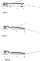
- Figure 1 refers to the first state of the present embodiment of the invention wherein the non-volatile memory cell arrangement 1 comprises: a micromechanical element 2, such as a cantilever in the present embodiment; a support portion 3 of the element 2 disposed on a first electrode 4; the free end of the element 2 is moveable above the second electrode 5 and third electrode 6; with electrodes 4, 5 and 6 being disposed in a coplanar arrangement.
- Z denotes the separation between the lower surface of the micromechanical element 2 and the upper surface of the electrodes 4, 5 and 6.
- Electrode 5 is a switching electrode while electrode 4 and electrode 6 function as contact electrodes. In the first state, no voltages are applied to the cell. Therefore, no electrostatic forces are present between element 2 and electrodes 4, 5 and 6, and hence the cell exists in a state of equilibrium in which element 2 remains stationary.
- element 2 of the non volatile memory cell 1 can be placed in a second state in which it can be activated to an ON state.
- This is achieved by the application of a biasing voltage V1, for example, at deflection electrode 5, which induces electrostatic forces between element 2 and electrode 5 urging element 2 towards contact electrode 6.
- V1 biasing voltage
- Contact is retained.... attraction such as, Van der Waals forces or surface tension collectively known as stiction or metal-to-metal bonding, which constitutes an energetically favourable adhesive state of cell 1 in this mode.
- the micromechanical structure 2 stores elastic energy and the memory cell 1 contains an additional energy component caused by the stiction forces generated at the interface between the element's tip and the contact electrode as described hereinbefore.
- electrodes may be coated with thin films of polymer to reduce adhesion energy between element 2 and 6.
- the nonvolatile memory cell 1 used in the method of the present invention undertakes another state step after the contact mode described hereinbefore.
- a biasing voltage V2 (V2>0 ⁇ 0) is applied between electrode 5 and element 2 while the element 2 is still in contact at electrode 6, thereby pulling-in element 2 further towards electrode 5.
- V2 biasing voltage
- additional elastic strain energy is generated and stored within one or more portions of element 2.
- the increase in elastic energy of the micromechanical element should be sufficient to surmount the adhesive forces present at the interface between element 2 and electrode 6. It should be noted that the applied voltage should control the displacement of the element in a manner so as to prevent direct contact of the micromechanical element 2 with electrode 5 as this would short the cell.
- element 2 is rapidly deflected in a direction away from the deflecting electrode 5 as shown in figure 4 .
- Elastic strain energy stored in element 2 counteracts the adhesive forces or stiction between it and contact electrode 6 thereby releasing the element 2 in a rapid release mode.
- the adhesive forces constitute an energy barrier at the interface between electrode 6 and element 2.
- the element 2 makes a transition from the energetically favourable adhesive state to a next state in which the element 2 can move freely. This is known as the de-programmed state.
- the program and de-program states are performed successively and repeatedly.
- the rapid release mode is an important aspect of the present invention, it is important that the application of a voltage to the deflection electrode 5 in the rapid release mode is sufficiently fast that the mechanical pulse propagation within the material should be the limiting factor, and this is related to the mechanical resonance frequency (1 st natural mode frequency) of the micromechanical element 2. This is because the stored elastic energy may undesirably dissipate to the extent that the rapid release of the micromechanical element may not be effected. It is undesirable to slow down the motion of the micromechanical element by having an electrical pulse falling at slower rate than the mechanical resonance, which mechanical resonance includes the effects of viscous damping and clamping support loss.
- micromechanical element 305 is arranged in proximity with another micromechanical element 310 grounded at 340 in circuit 300.
- Micromechanical element 310 has a pull-in electrode 350 and a contact electrode 355, while micromechanical element 305 has a contact electrode 345 and pull-in electrode 355 which is the contact electrode of micromechanical element 310.
- micromechanical element 305 In normal operation of the device, as described hereinbefore with reference to figure 5 , as micromechanical element 305 is pulled in, by the driving/sensing circuit 320, at a deflecting voltage V1 (V>0) 325, and then pulled in further by a voltage supplied at V2 325 in the next step to increase the elastic strain energy and subsequently cause rapid release of micromechanical element 305.
- V1 V>0
- V2 voltage supplied at V2 325
- the rapid release mode mechanism is much more effective if the touching area between the micromechanical element and the electrode is minimized.
- the tip of the micromechanical element should touch the contact electrode during the de-programming cycle so as to ensure that it does not snap down into the 'flat' mode, that is, contact the pull-in electrode. This can be achieved by several methods including the provision of a stiff section proximal to the tip to prevent flat mode.
- the deflection during the rapid release mode of the micromechanical element may be enhanced by providing a structure having variations in bending stiffness along its length.
- the length 2 of the segment may be made of a material having a high bending stiffness because this segment is pulled in further during the metastable mode.
- the other lengths of the structure, length B and length C may each have a predetermined bending stiffness to accommodate the higher bending stiffness in the length B, so as to maintain the structural integrity of the micromechanical element 5.
- the voltage pulses applied to the cell 1 of figure 1-4 can be reduced in order to reduce power consumption.
- a lower biasing voltage may be applied at electrode 5 to pull in the structural element 2 so as to effect electrical contact thereof with electrode 6.
- the separation Z should be such that there is no contact between the electrode 5 and the element 2, which would cause undesirable shorting of the electrode 5 and cause premature de-activation of the device.
- the inter-electrode spacing of the cell can be altered to change the amount of elastic strain energy stored in element 2. For example, if electrode 5 is situated further from the electrode 6, the micromechanical element 2 may be pulled in further owing to the lower probability that it may come into contact with electrode 5 before rapid release. This would cause shorting of the electrode 5.
- the micromechanical element 600 may comprise one or more parallel beam segments, for example, segment 601, segment 602 and segment 603.
- the element 600 is responsive to electrodes 604 and 604 arranged laterally to each other. In use, as the structure undergoes the metastable state as described hereinbefore, that is, the structure is pulled down under the influence of electrodes 604 and 605 and warps further prior to release resulting in increased bending stiffness along the length.
- the twisted side beams have increased bending stiffness.
- the arrangement of the present embodiment minimizes the pull down effect while the torsional moment is maximized on the side beams. Consequently more elastic strain energy can be induced into the system corresponding to the same amount of vertical deflection than in case of the micromechanical element of the present invention.
Landscapes
- Micromachines (AREA)
- Semiconductor Memories (AREA)
Description
- The present invention relates to a method for controlling micromechanical elements, for use in nonvolatile memory devices.
- Because of this drive to minaturise devices in highly integrated circuits for microelectronics applications, there exists a tremendous potential for the use of micromechanical structures or elements in applications such as switches, capacitors and relays in the microelectronics industry. Micromechanical elements such as cantilevers, for use in memory devices, are the primary contenders for solid state memory arrays found in semiconductor chips.
- In addition, micromechanical structures are being adopted for a variety of applications including micro-switches, capacitance circuits, accelerometers and optical elements. Owing to the progressive advances in fabrication techniques, micromechanical structures have been significantly reduced in size which has consequently raised their potential as logic elements or memory elements to compete with semiconductor processor and memory chips.
- Conventional semiconductor non-volatile memories can be written to and erased by use of transistors having a floating gate and a control gate separated by and insulator. Charge stored on the floating gate may represent a binary value, which is determined by whether or not a predetermined voltage known as the threshold voltage has been exceeded at which time the device is switched ON.
- A conventional solid state memory has storage cells which can assume either an ON state or an OFF state to represent information storage states. Charge transfer within the memory transistor defines one bit of information during the ON and OFF states, which is determined by the aforementioned threshold voltages applied to the memory transistors.
- The value of micromechanical elements predominates in their small size and their potential for use, for example, as micromechanical structures that provide a medium for charge transfer for use in memory applications. It is desirable to provide a micromechanical element having good structural integrity and is reliable in switching operations. The micromechanical element is typically housed in a low pressure elongate cavity wherein it is movable and can be switched ON and OFF by the application of an actuating voltage which brings the element into and out of contact respectively with a contiguous electrode(s). This arrangement is generally known as a cell.
- One of the key problems facing the performance of micromechanical contact switches/cells is that in an ON state an electrode and a micro-electromechanical element tend to stick to each other upon contact, making it difficult to separate them so as to switch the cell off, for example. The skilled addressee in the micro-electromechanical systems (MEMS) field refers to this phenomenon as "stiction", which is caused by the attraction between atoms and molecules of the two different surfaces. Where the deflection is electrostatic, high control voltages, typically as high as 40V compared with integrated circuits operating at voltages of about 5V or 3.3V, are required to induce a restoring force.
- The non-volatile memory arrangement of the present invention exploits stiction between the cantilever switch and the electrode to keep the switch in the ON state. Cantilever-based relays, for example, are usually actuated to an ON state by maintaining a constant biasing voltage. However in order to relieve the micromechanical structure quickly from the ON state to an OFF state, most solutions invoke the OFF state by reducing the constant bias with the application of a negative pulse. Consequently to achieve the OFF state, a lower voltage is applied than that required to actuate the ON state.
- Although stiction is a significant problem in the MEMS field, research efforts are continuing in order to circumvent it in applications such as switches and memories. In the present invention, however, stiction is exploited to maintain adhesion between the micromechanical element and the contact electrode during the switching operation in order to program the structure. The present invention seeks to induce a greater controllable restoring force in a micromechanical element so as to program and deprogram it repeatedly, quickly and proficiently.
- The restoring force of a micro-electromechanical switch may be modified, for example, by the use of multiple control electrodes to pull it into contact with an electrode, or alternatively by implementing a specially shaped structural element to induce a stronger restoring force. But having more than one driving electrode increases the cost and complexity of the system employing such a switch.
WO99/63559 - In other solutions electrodes are disposed on each side of the movable micromechanical element as a means of effecting the switching operation. However, this solution has a number of limitations such as higher applied voltages, a larger cavity to house the electromechanical element, and where electrodes are disposed on each side of the structure necessitates the use of additional masks during the fabrication thereof and consequently increasing costs.
- Therefore, the object of the present invention is to provide a method for controlling a memory element disposed with an arrangement of electrodes, which permits rapid switching operation, a greater controllable restoring force in a micromechanical element so as to program and deprogram it repeatedly, quickly and proficiently, low switching voltages, and a low mask implementation in the fabrication steps of the structure to permit a smaller cavity to house the element coupled with a cost effective fabrication.
- Therefore, according to the first aspect of the present invention there is provided a method for controlling a nonvolatile memory arrangement, comprising: applying a first biasing voltage to a switching electrode to bend a micromechanical element and thereby move the micromechanical element from a first, de-programmed state spaced from a contact electrode to a second state in contact with the contact electrode and spaced a first distance from the switching electrode to generate stiction at the interface between the micromechanical element and the contact electrode and to render the micromechanical element to a programmed state; and applying a second biasing voltage to the switching electrode to further move the micromechanical element and increase the elastic strain energy of the micromechanical element to a value greater than the stiction at the interface between the micromechanical element and the contact electrode, wherein applying the second biasing voltage pulls the micromechanical element further towards the switching electrode; and rapidly dropping the second biasing voltage applied to the switching electrode to move the micromechanical element to the first, de-programmed state by counteracting the stiction at the interface between the micromechanical element and the contact electrode.
- Preferably, the deflection means comprises one or more coplanar electrodes.
- Preferably, the micromechanical element may be resiliently deformable in response to the deflection means and is made from a conducting material advantageously selected from a group of materials belonging to Titanium, Tungsten, Aluminium, Copper or Tantalum.
- Preferably, a first voltage may be applied to the deflection means to pull-in the micromechanical element so as to bring it into contact with a first electrode, and a second voltage is applied to the deflection means so as to bring the micromechanical element in proximity with the deflection means.
- Preferably, micromechanical element may comprise having different physical characteristics, more specifically it comprises portions having a higher bending stiffness from a next portion.
- Preferably, the step of applying the one or more control signals to the deflection means may move the micromechanical element into a contact state. Preferably, the steps of the method may include generating a predetermined signal for inducing the deflection of the micromechanical element in a direction away from a contact position in a rapid release mode.
- Advantageously, the step of generating the one or more predetermined signals to the deflection means moves the micromechanical element in proximity to the deflection means.
- The present invention is particularly advantageous compared with known solution in that the pull-in and pull-off electrodes are in the same plane. This has the implication that no extra masking step and extra layer during fabrication thereof are required for the de-programming of the switch. In addition to this, the electrostatic gap is also smaller under the programmed cantilever, which could result in lower de-programming voltages than that required in a configuration where the electrodes are disposed on each side of the micromechanical element.
- Embodiments of the present invention will now be described, by way of example only with reference to the accompanying drawings in which:
-
figure 1 shows non-volatile memory cell arrangement in which there is no application of voltage; -
figure 2 shows a cross section of the non-volatile memory cell arranged in a second state in which it can be activated to an ON state; -
figure 3 shows a cross section of the non-volatile memory device showing themicromechanical element 2 still in contact at an electrode, with the additional voltage thereby pulling-in the element further towards the electrode; -
figure 4 shows that when the voltage atelectrode 5 is dropped quickly, the micromechanical element is rapidly deflected in a direction away from the deflecting electrode; -
figure 5 shows the shorting circuit operable in the method of controlling the non-volatile device of the present invention; and -
figure 6 shows the micromechanical element comprising one or more parallel beam segments. - The present embodiment is described in terms of the different states that the memory cell, which is housed in a low pressure environment, undertakes to effect the integers of invention.
Figure 1 refers to the first state of the present embodiment of the invention wherein the non-volatilememory cell arrangement 1 comprises: amicromechanical element 2, such as a cantilever in the present embodiment; asupport portion 3 of theelement 2 disposed on afirst electrode 4; the free end of theelement 2 is moveable above thesecond electrode 5 andthird electrode 6; withelectrodes micromechanical element 2 and the upper surface of theelectrodes electrodes electrodes electrode 4 andelectrode 6 function as contact electrodes. In the first state, no voltages are applied to the cell. Therefore, no electrostatic forces are present betweenelement 2 andelectrodes element 2 remains stationary. - Referring to
figure 2 ,element 2 of the nonvolatile memory cell 1 can be placed in a second state in which it can be activated to an ON state. This is achieved by the application of a biasing voltage V1, for example, atdeflection electrode 5, which induces electrostatic forces betweenelement 2 andelectrode 5urging element 2 towardscontact electrode 6. When this "pull-in" voltage reaches a threshold value, theelement 2 can initiate charge transfer toelectrode 6 as a result of contact therebetween, which consequently renders theelement 2 in a programmed state. When the biasing voltage V1 is removed atelectrode 5 after programming, that is V1=0,element 2 remains in contact withelectrode 6. This is known as the programmed state. Contact is retained.... attraction such as, Van der Waals forces or surface tension collectively known as stiction or metal-to-metal bonding, which constitutes an energetically favourable adhesive state ofcell 1 in this mode. - Further, in this state the
micromechanical structure 2 stores elastic energy and thememory cell 1 contains an additional energy component caused by the stiction forces generated at the interface between the element's tip and the contact electrode as described hereinbefore. - It is useful for understanding the present invention and should be noted that in some applications such as volatile memories, stiction retaining contact between the
contact electrode 6 andelement 2 is not a desirable feature. Therefore, to counteract this, electrodes may be coated with thin films of polymer to reduce adhesion energy betweenelement - The
nonvolatile memory cell 1 used in the method of the present invention, undertakes another state step after the contact mode described hereinbefore. Referring tofigure 3 , a biasing voltage V2 (V2>0 < 0) is applied betweenelectrode 5 andelement 2 while theelement 2 is still in contact atelectrode 6, thereby pulling-inelement 2 further towardselectrode 5. Aselement 2 bends towardselectrode 5, additional elastic strain energy is generated and stored within one or more portions ofelement 2. The increase in elastic energy of the micromechanical element should be sufficient to surmount the adhesive forces present at the interface betweenelement 2 andelectrode 6. It should be noted that the applied voltage should control the displacement of the element in a manner so as to prevent direct contact of themicromechanical element 2 withelectrode 5 as this would short the cell. - In a further step, when voltage V2 at
electrode 5 is dropped quickly (|V|→0),element 2 is rapidly deflected in a direction away from the deflectingelectrode 5 as shown infigure 4 . Elastic strain energy stored inelement 2 counteracts the adhesive forces or stiction between it andcontact electrode 6 thereby releasing theelement 2 in a rapid release mode. The adhesive forces constitute an energy barrier at the interface betweenelectrode 6 andelement 2. In this mode theelement 2 makes a transition from the energetically favourable adhesive state to a next state in which theelement 2 can move freely. This is known as the de-programmed state. The program and de-program states are performed successively and repeatedly. - While the rapid release mode is an important aspect of the present invention, it is important that the application of a voltage to the
deflection electrode 5 in the rapid release mode is sufficiently fast that the mechanical pulse propagation within the material should be the limiting factor, and this is related to the mechanical resonance frequency (1st natural mode frequency) of themicromechanical element 2. This is because the stored elastic energy may undesirably dissipate to the extent that the rapid release of the micromechanical element may not be effected. It is undesirable to slow down the motion of the micromechanical element by having an electrical pulse falling at slower rate than the mechanical resonance, which mechanical resonance includes the effects of viscous damping and clamping support loss. - Moreover, if such a fast pulse cannot be supplied by the driving electronics of the memory cell, the 'pull-in electrode' of one micromechanical element can be shorted by another micromechanical element. Referring to
figure 5 , in circuit 300 themicromechanical element 305 is arranged in proximity with anothermicromechanical element 310 grounded at 340 in circuit 300.Micromechanical element 310 has a pull-in electrode 350 and acontact electrode 355, whilemicromechanical element 305 has acontact electrode 345 and pull-inelectrode 355 which is the contact electrode ofmicromechanical element 310. - In normal operation of the device, as described hereinbefore with reference to
figure 5 , asmicromechanical element 305 is pulled in, by the driving/sensing circuit 320, at a deflecting voltage V1 (V>0) 325, and then pulled in further by a voltage supplied atV2 325 in the next step to increase the elastic strain energy and subsequently cause rapid release ofmicromechanical element 305. Whenmicromechanical element 310 makes contact with the pull-inelectrode 355 ofmicromechanical element 305, the pull-inelectrode 355 is shorted and its voltage falls rapidly to zero owing to the large resistor 335 which limits the current atmicromechanical element 310. - The rapid release mode mechanism is much more effective if the touching area between the micromechanical element and the electrode is minimized. Thus only the tip of the micromechanical element should touch the contact electrode during the de-programming cycle so as to ensure that it does not snap down into the 'flat' mode, that is, contact the pull-in electrode. This can be achieved by several methods including the provision of a stiff section proximal to the tip to prevent flat mode.
- Therefore, in yet a further embodiment of the present invention, the deflection during the rapid release mode of the micromechanical element may be enhanced by providing a structure having variations in bending stiffness along its length. For example, referring back to the micromechanical cell of
figure 1 , thelength 2 of the segment may be made of a material having a high bending stiffness because this segment is pulled in further during the metastable mode. The other lengths of the structure, length B and length C, may each have a predetermined bending stiffness to accommodate the higher bending stiffness in the length B, so as to maintain the structural integrity of themicromechanical element 5. - In addition to this, there are a number of ways in which the voltage pulses applied to the
cell 1 offigure 1-4 can be reduced in order to reduce power consumption. Referring again tofigures 1 , by reducing the displacement Z between the lower surface ofmicromechanical element 2 and the electrodes, a lower biasing voltage may be applied atelectrode 5 to pull in thestructural element 2 so as to effect electrical contact thereof withelectrode 6. However, the separation Z should be such that there is no contact between theelectrode 5 and theelement 2, which would cause undesirable shorting of theelectrode 5 and cause premature de-activation of the device. - Referring to
figures 1-4 , the inter-electrode spacing of the cell can be altered to change the amount of elastic strain energy stored inelement 2. For example, ifelectrode 5 is situated further from theelectrode 6, themicromechanical element 2 may be pulled in further owing to the lower probability that it may come into contact withelectrode 5 before rapid release. This would cause shorting of theelectrode 5. - One of the primary objectives of the present inventions is to augment the elastic strain energy stored in the micromechanical element to enhance the speed of release thereof from the contact electrode. Referring to
figure 6 , in yet a further embodiment of the present invention, themicromechanical element 600 may comprise one or more parallel beam segments, for example,segment 601,segment 602 andsegment 603. Theelement 600 is responsive toelectrodes electrodes - With
segment 602 arranged in this way, the twisted side beams have increased bending stiffness. In addition, the arrangement of the present embodiment minimizes the pull down effect while the torsional moment is maximized on the side beams. Consequently more elastic strain energy can be induced into the system corresponding to the same amount of vertical deflection than in case of the micromechanical element of the present invention. - Although a particular embodiment is described herein for a method of controlling a micromechanical memory element, it is not intended that such specific references be considered as limitations upon the scope of this invention.
- Furthermore, having described the invention in connection with certain specific embodiments thereof, it is to be understood that further modifications may now suggest themselves to those skilled in the art. The invention is defined in the appended claims.
Claims (4)
- A method for controlling a nonvolatile memory arrangement, comprising:applying a first biasing voltage to a switching electrode (5) to bend a micromechanical element and therebymove the micromechanical element (2) from a first, de-programmed state spaced from a contact electrode (6) to a second state in contact with the contact electrode and spaced a first distance from the switching electrode to generate stiction at the interface between the micromechanical element and the contact electrode and to render the micromechanical element to a programmed state; andapplying a second biasing voltage to the switching electrode to further move the micromechanical element and increase the elastic strain energy of the micromechanical element to a value greater than the stiction at the interface between the micromechanical element and the contact electrode, wherein applying the second biasing voltage pulls the micromechanical element further towards the switching electrode; andrapidly dropping the second biasing voltage applied to the switching electrode to move the micromechanical element to the first, de-programmed state by counteracting the stiction at the interface between the micromechanical element and the contact electrode.
- The method of claim 1, wherein the first state is a stable state and the second state is a stable state.
- The method of claim 1, wherein the micromechanical element (2) has a first portion having a first bending stiffness and a second portion having a second bending stiffness that is greater than the first bending stiffness.
- The method of claim 1, further comprising charge transferring from the micromechanical element (2) to the contact electrode (6) to program the micromechanical element.
Applications Claiming Priority (3)
| Application Number | Priority Date | Filing Date | Title |
|---|---|---|---|
| GBGB0413341.9A GB0413341D0 (en) | 2004-06-15 | 2004-06-15 | Arrangement and method for controlling a micromechanical element |
| EP05748344.8A EP1756844B1 (en) | 2004-06-15 | 2005-05-20 | Method for controlling a micromechanical element |
| PCT/EP2005/005484 WO2005124803A1 (en) | 2004-06-15 | 2005-05-20 | Arrangement and method for controlling a micromechanical element |
Related Parent Applications (3)
| Application Number | Title | Priority Date | Filing Date |
|---|---|---|---|
| EP05748344.8A Division-Into EP1756844B1 (en) | 2004-06-15 | 2005-05-20 | Method for controlling a micromechanical element |
| EP05748344.8A Division EP1756844B1 (en) | 2004-06-15 | 2005-05-20 | Method for controlling a micromechanical element |
| EP05748344.8 Division | 2005-05-20 |
Publications (3)
| Publication Number | Publication Date |
|---|---|
| EP2211362A1 EP2211362A1 (en) | 2010-07-28 |
| EP2211362B1 true EP2211362B1 (en) | 2020-03-11 |
| EP2211362B8 EP2211362B8 (en) | 2021-07-07 |
Family
ID=32749922
Family Applications (2)
| Application Number | Title | Priority Date | Filing Date |
|---|---|---|---|
| EP10160530.1A Expired - Lifetime EP2211362B8 (en) | 2004-06-15 | 2005-05-20 | Method for controlling a micromechanical element |
| EP05748344.8A Expired - Lifetime EP1756844B1 (en) | 2004-06-15 | 2005-05-20 | Method for controlling a micromechanical element |
Family Applications After (1)
| Application Number | Title | Priority Date | Filing Date |
|---|---|---|---|
| EP05748344.8A Expired - Lifetime EP1756844B1 (en) | 2004-06-15 | 2005-05-20 | Method for controlling a micromechanical element |
Country Status (6)
| Country | Link |
|---|---|
| US (2) | US7613039B2 (en) |
| EP (2) | EP2211362B8 (en) |
| JP (1) | JP4995719B2 (en) |
| CN (2) | CN1961393A (en) |
| GB (1) | GB0413341D0 (en) |
| WO (1) | WO2005124803A1 (en) |
Families Citing this family (10)
| Publication number | Priority date | Publication date | Assignee | Title |
|---|---|---|---|---|
| GB0413341D0 (en) * | 2004-06-15 | 2004-07-21 | Cavendish Kinetics B V | Arrangement and method for controlling a micromechanical element |
| GB0523645D0 (en) * | 2005-11-21 | 2005-12-28 | Cavendish Kinetics Ltd | Structure & apparatus for a semiconductor device |
| KR100790822B1 (en) * | 2006-08-07 | 2008-01-02 | 삼성전자주식회사 | Nonvolatile Memory Device and Manufacturing Method Thereof |
| KR100840644B1 (en) * | 2006-12-29 | 2008-06-24 | 동부일렉트로닉스 주식회사 | Switching element and manufacturing method thereof |
| US7929341B2 (en) * | 2008-03-24 | 2011-04-19 | Samsung Electronics Co., Ltd. | Electromechanical switch and method of forming the same |
| US8957485B2 (en) * | 2009-01-21 | 2015-02-17 | Cavendish Kinetics, Ltd. | Fabrication of MEMS based cantilever switches by employing a split layer cantilever deposition scheme |
| US8289674B2 (en) | 2009-03-17 | 2012-10-16 | Cavendish Kinetics, Ltd. | Moving a free-standing structure between high and low adhesion states |
| KR101369028B1 (en) | 2010-02-12 | 2014-02-28 | 카오카부시키가이샤 | Cleaning device |
| CN112216454B (en) * | 2020-09-23 | 2021-12-07 | 东南大学 | High-resolution wide-range micro mechanical potentiometer leading-out structure and method |
| TWI783637B (en) * | 2021-08-18 | 2022-11-11 | 中光電智能感測股份有限公司 | Micro scanning mirror |
Family Cites Families (15)
| Publication number | Priority date | Publication date | Assignee | Title |
|---|---|---|---|---|
| US4674180A (en) * | 1984-05-01 | 1987-06-23 | The Foxboro Company | Method of making a micromechanical electric shunt |
| GB9309327D0 (en) * | 1993-05-06 | 1993-06-23 | Smith Charles G | Bi-stable memory element |
| US6115231A (en) * | 1997-11-25 | 2000-09-05 | Tdk Corporation | Electrostatic relay |
| JP4966448B2 (en) * | 1998-06-04 | 2012-07-04 | キャベンディッシュ キネティクス リミテッド | Micromechanical element |
| AU2565800A (en) * | 1999-03-18 | 2000-10-04 | Cavendish Kinetics Limited | Flash memory cell having a flexible element |
| US6229683B1 (en) * | 1999-06-30 | 2001-05-08 | Mcnc | High voltage micromachined electrostatic switch |
| FI109155B (en) * | 2000-04-13 | 2002-05-31 | Nokia Corp | Method and apparatus for controlling a micromechanical element |
| US6535091B2 (en) * | 2000-11-07 | 2003-03-18 | Sarnoff Corporation | Microelectronic mechanical systems (MEMS) switch and method of fabrication |
| US6473361B1 (en) * | 2000-11-10 | 2002-10-29 | Xerox Corporation | Electromechanical memory cell |
| US6625047B2 (en) * | 2000-12-31 | 2003-09-23 | Texas Instruments Incorporated | Micromechanical memory element |
| EP1227496A1 (en) * | 2001-01-17 | 2002-07-31 | Cavendish Kinetics Limited | Non-volatile memory |
| US6646215B1 (en) * | 2001-06-29 | 2003-11-11 | Teravicin Technologies, Inc. | Device adapted to pull a cantilever away from a contact structure |
| US6531668B1 (en) * | 2001-08-30 | 2003-03-11 | Intel Corporation | High-speed MEMS switch with high-resonance-frequency beam |
| US6744338B2 (en) * | 2001-11-13 | 2004-06-01 | International Business Machines Corporation | Resonant operation of MEMS switch |
| GB0413341D0 (en) * | 2004-06-15 | 2004-07-21 | Cavendish Kinetics B V | Arrangement and method for controlling a micromechanical element |
-
2004
- 2004-06-15 GB GBGB0413341.9A patent/GB0413341D0/en not_active Ceased
-
2005
- 2005-05-20 US US11/579,239 patent/US7613039B2/en active Active
- 2005-05-20 EP EP10160530.1A patent/EP2211362B8/en not_active Expired - Lifetime
- 2005-05-20 WO PCT/EP2005/005484 patent/WO2005124803A1/en not_active Ceased
- 2005-05-20 EP EP05748344.8A patent/EP1756844B1/en not_active Expired - Lifetime
- 2005-05-20 CN CNA2005800176987A patent/CN1961393A/en active Pending
- 2005-05-20 JP JP2007515803A patent/JP4995719B2/en not_active Expired - Lifetime
- 2005-05-20 CN CN2009101685202A patent/CN101714410B/en not_active Expired - Lifetime
-
2009
- 2009-10-09 US US12/576,267 patent/US7965547B2/en not_active Expired - Lifetime
Non-Patent Citations (1)
| Title |
|---|
| None * |
Also Published As
| Publication number | Publication date |
|---|---|
| GB0413341D0 (en) | 2004-07-21 |
| US7965547B2 (en) | 2011-06-21 |
| EP1756844B1 (en) | 2019-11-20 |
| WO2005124803A1 (en) | 2005-12-29 |
| US20100080052A1 (en) | 2010-04-01 |
| CN1961393A (en) | 2007-05-09 |
| EP2211362A1 (en) | 2010-07-28 |
| EP2211362B8 (en) | 2021-07-07 |
| CN101714410B (en) | 2013-02-13 |
| JP2008503075A (en) | 2008-01-31 |
| CN101714410A (en) | 2010-05-26 |
| EP1756844A1 (en) | 2007-02-28 |
| JP4995719B2 (en) | 2012-08-08 |
| US20070223267A1 (en) | 2007-09-27 |
| US7613039B2 (en) | 2009-11-03 |
Similar Documents
| Publication | Publication Date | Title |
|---|---|---|
| US7965547B2 (en) | Arrangement and method for controlling a micromechanical element | |
| US6473361B1 (en) | Electromechanical memory cell | |
| US7821363B2 (en) | Method and apparatus for bending electrostatic switch | |
| US7898371B2 (en) | Electromechanical switch with partially rigidified electrode | |
| US20080277718A1 (en) | 1T MEMS scalable memory cell | |
| EP1490294A1 (en) | Nanotube relay device | |
| US20100182120A1 (en) | Mems device with bi-directional element | |
| EP2270813B1 (en) | Non-volatile memory | |
| US7547883B2 (en) | Seek-scan probe (SSP) memory including mechanism for track correction | |
| US8339013B2 (en) | Semiconductor device and method of controlling electrostatic actuator | |
| KR100621827B1 (en) | Nonvolatile Mechanical Memory | |
| US20070247018A1 (en) | Electrostatic actuation method and electrostatic actuator with integral electrodes for microelectromechanical systems | |
| EP2396785B1 (en) | High-speed electrostatic actuation of mems-based devices | |
| US9165932B2 (en) | Memory cell and method of manufacturing a memory cell | |
| US7622780B2 (en) | Seek-scan probe (SSP) including see-saw scan probe with redundant tip | |
| JP2015521792A (en) | MEMS life improvement | |
| KR20200019291A (en) | Nem memory cell, nem memory device including the same and manufacturing method of nem memory cell | |
| US9160333B2 (en) | Capacitive microelectromechanical switches with dynamic soft-landing | |
| WO2003028058A1 (en) | A micromechanical switch and method of manufacturing the same | |
| EP4020471B1 (en) | Tape based storage device | |
| KR102605542B1 (en) | Low voltage electromechanical switch based on dynamic slingshot operation and method of same | |
| Qian et al. | Nanoelectromechanical switches | |
| Islam | Cantilever-based MEMS Actuator for Non-Volatile Memory Applications |
Legal Events
| Date | Code | Title | Description |
|---|---|---|---|
| PUAI | Public reference made under article 153(3) epc to a published international application that has entered the european phase |
Free format text: ORIGINAL CODE: 0009012 |
|
| AC | Divisional application: reference to earlier application |
Ref document number: 1756844 Country of ref document: EP Kind code of ref document: P |
|
| AK | Designated contracting states |
Kind code of ref document: A1 Designated state(s): AT BE BG CH CY CZ DE DK EE ES FI FR GB GR HU IE IS IT LI LT LU MC NL PL PT RO SE SI SK TR |
|
| 17P | Request for examination filed |
Effective date: 20110119 |
|
| 17Q | First examination report despatched |
Effective date: 20150520 |
|
| GRAP | Despatch of communication of intention to grant a patent |
Free format text: ORIGINAL CODE: EPIDOSNIGR1 |
|
| STAA | Information on the status of an ep patent application or granted ep patent |
Free format text: STATUS: GRANT OF PATENT IS INTENDED |
|
| INTG | Intention to grant announced |
Effective date: 20190930 |
|
| GRAS | Grant fee paid |
Free format text: ORIGINAL CODE: EPIDOSNIGR3 |
|
| GRAA | (expected) grant |
Free format text: ORIGINAL CODE: 0009210 |
|
| STAA | Information on the status of an ep patent application or granted ep patent |
Free format text: STATUS: THE PATENT HAS BEEN GRANTED |
|
| AC | Divisional application: reference to earlier application |
Ref document number: 1756844 Country of ref document: EP Kind code of ref document: P |
|
| AK | Designated contracting states |
Kind code of ref document: B1 Designated state(s): AT BE BG CH CY CZ DE DK EE ES FI FR GB GR HU IE IS IT LI LT LU MC NL PL PT RO SE SI SK TR |
|
| REG | Reference to a national code |
Ref country code: GB Ref legal event code: FG4D |
|
| REG | Reference to a national code |
Ref country code: CH Ref legal event code: EP |
|
| REG | Reference to a national code |
Ref country code: AT Ref legal event code: REF Ref document number: 1244167 Country of ref document: AT Kind code of ref document: T Effective date: 20200315 |
|
| REG | Reference to a national code |
Ref country code: DE Ref legal event code: R096 Ref document number: 602005056688 Country of ref document: DE |
|
| REG | Reference to a national code |
Ref country code: IE Ref legal event code: FG4D |
|
| PG25 | Lapsed in a contracting state [announced via postgrant information from national office to epo] |
Ref country code: FI Free format text: LAPSE BECAUSE OF FAILURE TO SUBMIT A TRANSLATION OF THE DESCRIPTION OR TO PAY THE FEE WITHIN THE PRESCRIBED TIME-LIMIT Effective date: 20200311 |
|
| REG | Reference to a national code |
Ref country code: NL Ref legal event code: MP Effective date: 20200311 |
|
| PG25 | Lapsed in a contracting state [announced via postgrant information from national office to epo] |
Ref country code: BG Free format text: LAPSE BECAUSE OF FAILURE TO SUBMIT A TRANSLATION OF THE DESCRIPTION OR TO PAY THE FEE WITHIN THE PRESCRIBED TIME-LIMIT Effective date: 20200611 Ref country code: SE Free format text: LAPSE BECAUSE OF FAILURE TO SUBMIT A TRANSLATION OF THE DESCRIPTION OR TO PAY THE FEE WITHIN THE PRESCRIBED TIME-LIMIT Effective date: 20200311 Ref country code: GR Free format text: LAPSE BECAUSE OF FAILURE TO SUBMIT A TRANSLATION OF THE DESCRIPTION OR TO PAY THE FEE WITHIN THE PRESCRIBED TIME-LIMIT Effective date: 20200612 |
|
| REG | Reference to a national code |
Ref country code: LT Ref legal event code: MG4D |
|
| PG25 | Lapsed in a contracting state [announced via postgrant information from national office to epo] |
Ref country code: NL Free format text: LAPSE BECAUSE OF FAILURE TO SUBMIT A TRANSLATION OF THE DESCRIPTION OR TO PAY THE FEE WITHIN THE PRESCRIBED TIME-LIMIT Effective date: 20200311 |
|
| PG25 | Lapsed in a contracting state [announced via postgrant information from national office to epo] |
Ref country code: LT Free format text: LAPSE BECAUSE OF FAILURE TO SUBMIT A TRANSLATION OF THE DESCRIPTION OR TO PAY THE FEE WITHIN THE PRESCRIBED TIME-LIMIT Effective date: 20200311 Ref country code: PT Free format text: LAPSE BECAUSE OF FAILURE TO SUBMIT A TRANSLATION OF THE DESCRIPTION OR TO PAY THE FEE WITHIN THE PRESCRIBED TIME-LIMIT Effective date: 20200805 Ref country code: IS Free format text: LAPSE BECAUSE OF FAILURE TO SUBMIT A TRANSLATION OF THE DESCRIPTION OR TO PAY THE FEE WITHIN THE PRESCRIBED TIME-LIMIT Effective date: 20200711 Ref country code: SK Free format text: LAPSE BECAUSE OF FAILURE TO SUBMIT A TRANSLATION OF THE DESCRIPTION OR TO PAY THE FEE WITHIN THE PRESCRIBED TIME-LIMIT Effective date: 20200311 Ref country code: RO Free format text: LAPSE BECAUSE OF FAILURE TO SUBMIT A TRANSLATION OF THE DESCRIPTION OR TO PAY THE FEE WITHIN THE PRESCRIBED TIME-LIMIT Effective date: 20200311 Ref country code: CZ Free format text: LAPSE BECAUSE OF FAILURE TO SUBMIT A TRANSLATION OF THE DESCRIPTION OR TO PAY THE FEE WITHIN THE PRESCRIBED TIME-LIMIT Effective date: 20200311 Ref country code: EE Free format text: LAPSE BECAUSE OF FAILURE TO SUBMIT A TRANSLATION OF THE DESCRIPTION OR TO PAY THE FEE WITHIN THE PRESCRIBED TIME-LIMIT Effective date: 20200311 |
|
| REG | Reference to a national code |
Ref country code: AT Ref legal event code: MK05 Ref document number: 1244167 Country of ref document: AT Kind code of ref document: T Effective date: 20200311 |
|
| REG | Reference to a national code |
Ref country code: DE Ref legal event code: R097 Ref document number: 602005056688 Country of ref document: DE |
|
| PLBE | No opposition filed within time limit |
Free format text: ORIGINAL CODE: 0009261 |
|
| STAA | Information on the status of an ep patent application or granted ep patent |
Free format text: STATUS: NO OPPOSITION FILED WITHIN TIME LIMIT |
|
| PG25 | Lapsed in a contracting state [announced via postgrant information from national office to epo] |
Ref country code: IT Free format text: LAPSE BECAUSE OF FAILURE TO SUBMIT A TRANSLATION OF THE DESCRIPTION OR TO PAY THE FEE WITHIN THE PRESCRIBED TIME-LIMIT Effective date: 20200311 Ref country code: MC Free format text: LAPSE BECAUSE OF FAILURE TO SUBMIT A TRANSLATION OF THE DESCRIPTION OR TO PAY THE FEE WITHIN THE PRESCRIBED TIME-LIMIT Effective date: 20200311 Ref country code: AT Free format text: LAPSE BECAUSE OF FAILURE TO SUBMIT A TRANSLATION OF THE DESCRIPTION OR TO PAY THE FEE WITHIN THE PRESCRIBED TIME-LIMIT Effective date: 20200311 Ref country code: DK Free format text: LAPSE BECAUSE OF FAILURE TO SUBMIT A TRANSLATION OF THE DESCRIPTION OR TO PAY THE FEE WITHIN THE PRESCRIBED TIME-LIMIT Effective date: 20200311 Ref country code: LI Free format text: LAPSE BECAUSE OF NON-PAYMENT OF DUE FEES Effective date: 20200531 Ref country code: ES Free format text: LAPSE BECAUSE OF FAILURE TO SUBMIT A TRANSLATION OF THE DESCRIPTION OR TO PAY THE FEE WITHIN THE PRESCRIBED TIME-LIMIT Effective date: 20200311 Ref country code: CH Free format text: LAPSE BECAUSE OF NON-PAYMENT OF DUE FEES Effective date: 20200531 |
|
| 26N | No opposition filed |
Effective date: 20201214 |
|
| PG25 | Lapsed in a contracting state [announced via postgrant information from national office to epo] |
Ref country code: PL Free format text: LAPSE BECAUSE OF FAILURE TO SUBMIT A TRANSLATION OF THE DESCRIPTION OR TO PAY THE FEE WITHIN THE PRESCRIBED TIME-LIMIT Effective date: 20200311 Ref country code: SI Free format text: LAPSE BECAUSE OF FAILURE TO SUBMIT A TRANSLATION OF THE DESCRIPTION OR TO PAY THE FEE WITHIN THE PRESCRIBED TIME-LIMIT Effective date: 20200311 |
|
| REG | Reference to a national code |
Ref country code: BE Ref legal event code: MM Effective date: 20200531 |
|
| PG25 | Lapsed in a contracting state [announced via postgrant information from national office to epo] |
Ref country code: LU Free format text: LAPSE BECAUSE OF NON-PAYMENT OF DUE FEES Effective date: 20200519 |
|
| PG25 | Lapsed in a contracting state [announced via postgrant information from national office to epo] |
Ref country code: IE Free format text: LAPSE BECAUSE OF NON-PAYMENT OF DUE FEES Effective date: 20200519 |
|
| GRAT | Correction requested after decision to grant or after decision to maintain patent in amended form |
Free format text: ORIGINAL CODE: EPIDOSNCDEC |
|
| PG25 | Lapsed in a contracting state [announced via postgrant information from national office to epo] |
Ref country code: BE Free format text: LAPSE BECAUSE OF NON-PAYMENT OF DUE FEES Effective date: 20200531 |
|
| PLAA | Information modified related to event that no opposition was filed |
Free format text: ORIGINAL CODE: 0009299DELT |
|
| PLBE | No opposition filed within time limit |
Free format text: ORIGINAL CODE: 0009261 |
|
| R26N | No opposition filed (corrected) |
Effective date: 20201214 |
|
| PGFP | Annual fee paid to national office [announced via postgrant information from national office to epo] |
Ref country code: GB Payment date: 20210428 Year of fee payment: 17 |
|
| PG25 | Lapsed in a contracting state [announced via postgrant information from national office to epo] |
Ref country code: TR Free format text: LAPSE BECAUSE OF FAILURE TO SUBMIT A TRANSLATION OF THE DESCRIPTION OR TO PAY THE FEE WITHIN THE PRESCRIBED TIME-LIMIT Effective date: 20200311 Ref country code: CY Free format text: LAPSE BECAUSE OF FAILURE TO SUBMIT A TRANSLATION OF THE DESCRIPTION OR TO PAY THE FEE WITHIN THE PRESCRIBED TIME-LIMIT Effective date: 20200311 |
|
| REG | Reference to a national code |
Ref country code: GB Ref legal event code: 732E Free format text: REGISTERED BETWEEN 20220505 AND 20220512 |
|
| REG | Reference to a national code |
Ref country code: DE Ref legal event code: R081 Ref document number: 602005056688 Country of ref document: DE Owner name: QORVO INTERNATIONAL PTE. LTD., SG Free format text: FORMER OWNER: CAVENDISH-KINETICS B.V., 'S-HERTOGENBOSCH, NL Ref country code: DE Ref legal event code: R081 Ref document number: 602005056688 Country of ref document: DE Owner name: CAVENDISH-KINETICS B.V., NL Free format text: FORMER OWNER: CAVENDISH-KINETICS B.V., 'S-HERTOGENBOSCH, NL Ref country code: DE Ref legal event code: R081 Ref document number: 602005056688 Country of ref document: DE Owner name: QORVO US, INC., GREENSBORO, US Free format text: FORMER OWNER: CAVENDISH-KINETICS B.V., 'S-HERTOGENBOSCH, NL |
|
| REG | Reference to a national code |
Ref country code: DE Ref legal event code: R081 Ref document number: 602005056688 Country of ref document: DE Owner name: QORVO INTERNATIONAL PTE. LTD., SG Free format text: FORMER OWNER: QORVO US, INC., GREENSBORO, NC, US |
|
| REG | Reference to a national code |
Ref country code: DE Ref legal event code: R081 Ref document number: 602005056688 Country of ref document: DE Owner name: QORVO INTERNATIONAL PTE. LTD., SG Free format text: FORMER OWNER: CAVENDISH-KINETICS B.V., 'S-HERTOGENBOSCH, NL |
|
| GBPC | Gb: european patent ceased through non-payment of renewal fee |
Effective date: 20220519 |
|
| PG25 | Lapsed in a contracting state [announced via postgrant information from national office to epo] |
Ref country code: HU Free format text: LAPSE BECAUSE OF FAILURE TO SUBMIT A TRANSLATION OF THE DESCRIPTION OR TO PAY THE FEE WITHIN THE PRESCRIBED TIME-LIMIT Effective date: 20200311 Ref country code: GB Free format text: LAPSE BECAUSE OF NON-PAYMENT OF DUE FEES Effective date: 20220519 |
|
| PGFP | Annual fee paid to national office [announced via postgrant information from national office to epo] |
Ref country code: DE Payment date: 20240418 Year of fee payment: 20 |
|
| PGFP | Annual fee paid to national office [announced via postgrant information from national office to epo] |
Ref country code: FR Payment date: 20240418 Year of fee payment: 20 |
|
| REG | Reference to a national code |
Ref country code: DE Ref legal event code: R071 Ref document number: 602005056688 Country of ref document: DE |