EP1505859A2 - Multilayer printed wiring board having filled via-holes - Google Patents
Multilayer printed wiring board having filled via-holes Download PDFInfo
- Publication number
- EP1505859A2 EP1505859A2 EP04024664A EP04024664A EP1505859A2 EP 1505859 A2 EP1505859 A2 EP 1505859A2 EP 04024664 A EP04024664 A EP 04024664A EP 04024664 A EP04024664 A EP 04024664A EP 1505859 A2 EP1505859 A2 EP 1505859A2
- Authority
- EP
- European Patent Office
- Prior art keywords
- layer
- viahole
- wiring board
- printed wiring
- multilayer printed
- Prior art date
- Legal status (The legal status is an assumption and is not a legal conclusion. Google has not performed a legal analysis and makes no representation as to the accuracy of the status listed.)
- Granted
Links
Images


Classifications
-
- H—ELECTRICITY
- H05—ELECTRIC TECHNIQUES NOT OTHERWISE PROVIDED FOR
- H05K—PRINTED CIRCUITS; CASINGS OR CONSTRUCTIONAL DETAILS OF ELECTRIC APPARATUS; MANUFACTURE OF ASSEMBLAGES OF ELECTRICAL COMPONENTS
- H05K3/00—Apparatus or processes for manufacturing printed circuits
- H05K3/46—Manufacturing multilayer circuits
- H05K3/4644—Manufacturing multilayer circuits by building the multilayer layer by layer, i.e. build-up multilayer circuits
- H05K3/4661—Adding a circuit layer by direct wet plating, e.g. electroless plating; insulating materials adapted therefor
-
- H—ELECTRICITY
- H05—ELECTRIC TECHNIQUES NOT OTHERWISE PROVIDED FOR
- H05K—PRINTED CIRCUITS; CASINGS OR CONSTRUCTIONAL DETAILS OF ELECTRIC APPARATUS; MANUFACTURE OF ASSEMBLAGES OF ELECTRICAL COMPONENTS
- H05K3/00—Apparatus or processes for manufacturing printed circuits
- H05K3/46—Manufacturing multilayer circuits
-
- H—ELECTRICITY
- H05—ELECTRIC TECHNIQUES NOT OTHERWISE PROVIDED FOR
- H05K—PRINTED CIRCUITS; CASINGS OR CONSTRUCTIONAL DETAILS OF ELECTRIC APPARATUS; MANUFACTURE OF ASSEMBLAGES OF ELECTRICAL COMPONENTS
- H05K3/00—Apparatus or processes for manufacturing printed circuits
- H05K3/40—Forming printed elements for providing electric connections to or between printed circuits
- H05K3/42—Plated through-holes or plated via connections
- H05K3/421—Blind plated via connections
-
- H—ELECTRICITY
- H05—ELECTRIC TECHNIQUES NOT OTHERWISE PROVIDED FOR
- H05K—PRINTED CIRCUITS; CASINGS OR CONSTRUCTIONAL DETAILS OF ELECTRIC APPARATUS; MANUFACTURE OF ASSEMBLAGES OF ELECTRICAL COMPONENTS
- H05K2201/00—Indexing scheme relating to printed circuits covered by H05K1/00
- H05K2201/01—Dielectrics
- H05K2201/0104—Properties and characteristics in general
- H05K2201/0129—Thermoplastic polymer, e.g. auto-adhesive layer; Shaping of thermoplastic polymer
-
- H—ELECTRICITY
- H05—ELECTRIC TECHNIQUES NOT OTHERWISE PROVIDED FOR
- H05K—PRINTED CIRCUITS; CASINGS OR CONSTRUCTIONAL DETAILS OF ELECTRIC APPARATUS; MANUFACTURE OF ASSEMBLAGES OF ELECTRICAL COMPONENTS
- H05K2201/00—Indexing scheme relating to printed circuits covered by H05K1/00
- H05K2201/01—Dielectrics
- H05K2201/0137—Materials
- H05K2201/015—Fluoropolymer, e.g. polytetrafluoroethylene [PTFE]
-
- H—ELECTRICITY
- H05—ELECTRIC TECHNIQUES NOT OTHERWISE PROVIDED FOR
- H05K—PRINTED CIRCUITS; CASINGS OR CONSTRUCTIONAL DETAILS OF ELECTRIC APPARATUS; MANUFACTURE OF ASSEMBLAGES OF ELECTRICAL COMPONENTS
- H05K2201/00—Indexing scheme relating to printed circuits covered by H05K1/00
- H05K2201/02—Fillers; Particles; Fibers; Reinforcement materials
- H05K2201/0275—Fibers and reinforcement materials
- H05K2201/0278—Polymeric fibers
-
- H—ELECTRICITY
- H05—ELECTRIC TECHNIQUES NOT OTHERWISE PROVIDED FOR
- H05K—PRINTED CIRCUITS; CASINGS OR CONSTRUCTIONAL DETAILS OF ELECTRIC APPARATUS; MANUFACTURE OF ASSEMBLAGES OF ELECTRICAL COMPONENTS
- H05K2201/00—Indexing scheme relating to printed circuits covered by H05K1/00
- H05K2201/09—Shape and layout
- H05K2201/09209—Shape and layout details of conductors
- H05K2201/095—Conductive through-holes or vias
- H05K2201/09563—Metal filled via
-
- H—ELECTRICITY
- H05—ELECTRIC TECHNIQUES NOT OTHERWISE PROVIDED FOR
- H05K—PRINTED CIRCUITS; CASINGS OR CONSTRUCTIONAL DETAILS OF ELECTRIC APPARATUS; MANUFACTURE OF ASSEMBLAGES OF ELECTRICAL COMPONENTS
- H05K2201/00—Indexing scheme relating to printed circuits covered by H05K1/00
- H05K2201/09—Shape and layout
- H05K2201/09209—Shape and layout details of conductors
- H05K2201/095—Conductive through-holes or vias
- H05K2201/096—Vertically aligned vias, holes or stacked vias
-
- H—ELECTRICITY
- H05—ELECTRIC TECHNIQUES NOT OTHERWISE PROVIDED FOR
- H05K—PRINTED CIRCUITS; CASINGS OR CONSTRUCTIONAL DETAILS OF ELECTRIC APPARATUS; MANUFACTURE OF ASSEMBLAGES OF ELECTRICAL COMPONENTS
- H05K2201/00—Indexing scheme relating to printed circuits covered by H05K1/00
- H05K2201/09—Shape and layout
- H05K2201/09209—Shape and layout details of conductors
- H05K2201/09654—Shape and layout details of conductors covering at least two types of conductors provided for in H05K2201/09218 - H05K2201/095
- H05K2201/09745—Recess in conductor, e.g. in pad or in metallic substrate
-
- H—ELECTRICITY
- H05—ELECTRIC TECHNIQUES NOT OTHERWISE PROVIDED FOR
- H05K—PRINTED CIRCUITS; CASINGS OR CONSTRUCTIONAL DETAILS OF ELECTRIC APPARATUS; MANUFACTURE OF ASSEMBLAGES OF ELECTRICAL COMPONENTS
- H05K3/00—Apparatus or processes for manufacturing printed circuits
- H05K3/10—Apparatus or processes for manufacturing printed circuits in which conductive material is applied to the insulating support in such a manner as to form the desired conductive pattern
- H05K3/108—Apparatus or processes for manufacturing printed circuits in which conductive material is applied to the insulating support in such a manner as to form the desired conductive pattern by semi-additive methods; masks therefor
-
- H—ELECTRICITY
- H05—ELECTRIC TECHNIQUES NOT OTHERWISE PROVIDED FOR
- H05K—PRINTED CIRCUITS; CASINGS OR CONSTRUCTIONAL DETAILS OF ELECTRIC APPARATUS; MANUFACTURE OF ASSEMBLAGES OF ELECTRICAL COMPONENTS
- H05K3/00—Apparatus or processes for manufacturing printed circuits
- H05K3/38—Improvement of the adhesion between the insulating substrate and the metal
- H05K3/381—Improvement of the adhesion between the insulating substrate and the metal by special treatment of the substrate
-
- H—ELECTRICITY
- H05—ELECTRIC TECHNIQUES NOT OTHERWISE PROVIDED FOR
- H05K—PRINTED CIRCUITS; CASINGS OR CONSTRUCTIONAL DETAILS OF ELECTRIC APPARATUS; MANUFACTURE OF ASSEMBLAGES OF ELECTRICAL COMPONENTS
- H05K3/00—Apparatus or processes for manufacturing printed circuits
- H05K3/38—Improvement of the adhesion between the insulating substrate and the metal
- H05K3/382—Improvement of the adhesion between the insulating substrate and the metal by special treatment of the metal
-
- H—ELECTRICITY
- H05—ELECTRIC TECHNIQUES NOT OTHERWISE PROVIDED FOR
- H05K—PRINTED CIRCUITS; CASINGS OR CONSTRUCTIONAL DETAILS OF ELECTRIC APPARATUS; MANUFACTURE OF ASSEMBLAGES OF ELECTRICAL COMPONENTS
- H05K3/00—Apparatus or processes for manufacturing printed circuits
- H05K3/40—Forming printed elements for providing electric connections to or between printed circuits
- H05K3/42—Plated through-holes or plated via connections
- H05K3/423—Plated through-holes or plated via connections characterised by electroplating method
-
- Y—GENERAL TAGGING OF NEW TECHNOLOGICAL DEVELOPMENTS; GENERAL TAGGING OF CROSS-SECTIONAL TECHNOLOGIES SPANNING OVER SEVERAL SECTIONS OF THE IPC; TECHNICAL SUBJECTS COVERED BY FORMER USPC CROSS-REFERENCE ART COLLECTIONS [XRACs] AND DIGESTS
- Y10—TECHNICAL SUBJECTS COVERED BY FORMER USPC
- Y10T—TECHNICAL SUBJECTS COVERED BY FORMER US CLASSIFICATION
- Y10T428/00—Stock material or miscellaneous articles
- Y10T428/24—Structurally defined web or sheet [e.g., overall dimension, etc.]
- Y10T428/24273—Structurally defined web or sheet [e.g., overall dimension, etc.] including aperture
- Y10T428/24322—Composite web or sheet
-
- Y—GENERAL TAGGING OF NEW TECHNOLOGICAL DEVELOPMENTS; GENERAL TAGGING OF CROSS-SECTIONAL TECHNOLOGIES SPANNING OVER SEVERAL SECTIONS OF THE IPC; TECHNICAL SUBJECTS COVERED BY FORMER USPC CROSS-REFERENCE ART COLLECTIONS [XRACs] AND DIGESTS
- Y10—TECHNICAL SUBJECTS COVERED BY FORMER USPC
- Y10T—TECHNICAL SUBJECTS COVERED BY FORMER US CLASSIFICATION
- Y10T428/00—Stock material or miscellaneous articles
- Y10T428/24—Structurally defined web or sheet [e.g., overall dimension, etc.]
- Y10T428/24802—Discontinuous or differential coating, impregnation or bond [e.g., artwork, printing, retouched photograph, etc.]
- Y10T428/24917—Discontinuous or differential coating, impregnation or bond [e.g., artwork, printing, retouched photograph, etc.] including metal layer
-
- Y—GENERAL TAGGING OF NEW TECHNOLOGICAL DEVELOPMENTS; GENERAL TAGGING OF CROSS-SECTIONAL TECHNOLOGIES SPANNING OVER SEVERAL SECTIONS OF THE IPC; TECHNICAL SUBJECTS COVERED BY FORMER USPC CROSS-REFERENCE ART COLLECTIONS [XRACs] AND DIGESTS
- Y10—TECHNICAL SUBJECTS COVERED BY FORMER USPC
- Y10T—TECHNICAL SUBJECTS COVERED BY FORMER US CLASSIFICATION
- Y10T428/00—Stock material or miscellaneous articles
- Y10T428/31504—Composite [nonstructural laminate]
- Y10T428/31678—Of metal
- Y10T428/31681—Next to polyester, polyamide or polyimide [e.g., alkyd, glue, or nylon, etc.]
Definitions
- the present invention relates to a multilayer printed wiring board having a filled viahole structure, and more particularly to a multilayer printed wiring board adapted to assure an outstandingly secure adhesion between a conductor circuitry layer and an interlaminar insulative resin layer and form a fine conductor circuit pattern.
- the multilayer printed wiring board includes a build-up multilayer printed wiring board in which conductor circuitry layers and insulative resin layers are alternately formed one on another and inner and outer ones of the conductor circuitry layers are electrically connected to each other by viaholes formed in the insulative resin layers.
- the viaholes in such a multilayer printed wiring board are formed by depositing a plating metal film on the inner wall and bottom of each of fine holes formed through the interlaminar insulative resin layers.
- the multilayer printed wiring board having such viaholes formed through them are not advantageous in that the metal deposit is likely to break due to its precipitation or a heat cycle.
- it has recently been proposed to fill the viaholes with a platingmetal this structure will be referred to as "filled viahole structure” henceforth.
- filled viahole structures are known from the disclosure, for example, in the Japanese unexamined patent publication Nos. Hei 2-188992, Hei 3-3298 and Hei 7-34048.
- the multilayer printed wiring board having the filled viahole structure is however disadvantageous in that a surface portion of the plating metal exposed outside the hole for viahole (the surface will be referred to as "viahole surface” henceforth) is easily depressible. If an interlaminar rein insulating layer is formed on a conductor circuitry layer irrespectively of such a depression existent on the viahole surface, a corresponding depression will develop on the surface of the interlaminar insulative resin layer, and cause the plating metal film to break and also a trouble in mounting electronic parts on the wiring board.
- the viahole surface where such a depression or concavity exists or is likely to exist can be flattened by applying an interlaminar resin more than once.
- the application of the interlaminar resin will lead to a greater thickness of the interlaminar insulative resin layer just above the depression on the viahole surface than that of the interlaminar insulative resin layer on the conductor circuitry layer.
- the interlaminar resin will partially remain inside the hole to lower the electrical connection reliability of the viahole.
- the residual resin is likely tooccur since it is difficult to set different exposure and development conditions for the viahole surface from those for the conductor circuitry layer surface.
- a plating conductor or metal is filled in a hole for viahole so that a conductor circuitry layer has a thickness more than a half of the viahole diameter and thus the conductor circuitry layer surface is at a same level as the viahole surface.
- the inner wall of the hole formed in an interlaminar insulative resin layer should be plated with a thick layer of metal or conductor and thus a conductor circuitry layer formed along with the plating metal on the viahole will also be thick.
- the plating resin should also be correspondingly thicker.
- a plating metal is filled in a hole for viahole, a larger stress will be caused by heat cycle than in a viahole formed just by plating an inner wall and bottom of a hole, so that a crack is likely to occur first in the viahole and then spread to an interlaminar insulative resin layer.
- an electroless plating method is used to fill the plating metal into the hole for viahole.
- the plating layer applied by the electroless plating is harder and less malleable than a one applied by the electroplating. Therefore, the plating layer is likely to crack under a thermal shock or due to heat cycle.
- the boundary between the electroless plating and electroplating layers is flat so that both the plating layers are separable from each other under a thermal shock or due to heat cycle.
- a plating resist has to be formed before a hole for viahole is filled with a metal by the electroplating.
- the plating resist is formed on the electroless plating layer, the plating resist is easily separable and an inter-pattern shortcircuit will possibly take place.
- the present invention has a primary object to overcome the above-mentioned drawbacks of the prior art by providing a multilayer printed wiring board having a filled viahole structure adapted to form a fine conductor circuit pattern and provide a highly reliable electrical connection between conductive circuitry layers.
- the present invention has another object to provide a multilayer printed wiring board having a filled viahole structure adapted to assure a highly secure adhesion between a conductor circuitry layer and an interlaminar insulative resin layer and which will not crack even under a thermal shock or due to heat cycle.
- a build-up multilayer printed wiring board having conductor circuitry layers and interlaminar insulative resin layers deposited alternately one on another, the interlaminar insulative resin layers having formed through them holes each filled with a plating layer to form a viahole, the surface of the plating layer exposed out of the hole for the viahole (the surface will be referred to as "viahole surface” henceforth) being formed substantially flat and lying at a substantially same level as the surface of the conductor circuit layer disposed in the interlaminar insulative resin layer in which the viahole also lies, and the thickness of the conductor circuitry layer being less than a half of the viahole diameter.
- viahole diameter means an opening diameter of the hole for the viahole.
- the first embodiment having the above-mentioned filled viahole structure is advantageous as follows:
- a build-up multilayer printed wiring board having conductor circuitry layers and interlaminar insulative resin layers deposited alternately one on another, the interlaminar insulative resin layers having formed through them holes each filled with a plating layer to form a viahole, the thickness of the conductor circuitry layer being less than a half of the viahole diameter and less than 25 ⁇ m.
- the thickness of the plating conductor forming the conductor circuitry layer can be less than the half of the viahole and less than 25 ⁇ m.
- a thinner plating resist having an improved resolution, which enables to easily form the conductor circuitry by etching and pattern an ultra-fine circuit.
- the first and second embodiments of the present invention should preferably be constructed as follows:
- the depression thus formed will provide an obtuse angle defined between contact surface edges of a viahole and a further viahole formed on the preceding one. A stress to the viahole surface edges is thus dispersed, so that a crack can be prevented from taking place and spreading from the contact surface edges to the interlaminar insulative resin layer.
- the roughening of the depressed surface improves the adhesion between the viahole, conductor layer on which the conductor circuit is formed, and interlaminar insulative resin layer, which assures to prevent the conductor layer from separating from the other.
- a build-up multilayer printed wiring board having conductor circuitry layers and interlaminar insulative resin layers deposited alternately one on another, the interlaminar insulative resin layers having formed through them holes each filledwith a plating layer to form a viahole, the hole in the interlaminar insulative resin layer having at least an inner wall thereof roughened, the roughened inner wall of the hole being covered with an electroless plating layer, and an inner space of the hole defined by the electroless plating layer being filled with an electroplating layer to form the viahole.
- the electroless plating layer harder than the electroplating layer is formed over the inner wall of the hole.
- the electroless plating layer bites, like anchor, the roughened surface, so it is not easily broken even if applied with a separating force.
- the adhesion between the viahole and interlaminar insulative resin layer is improved.
- the electroplating layer having a larger malleability than the electroless plating layer fills the major part of the hole, the electroplating layer will flexibly follow the expansion and shrinkage of the interlaminar insulative resin layer, thus the layers can be prevented from being cracked under a thermal shock or due to heat cycle.
- an electroless plating layer formed on the roughened surface will have a correspondingly roughened surface.
- the roughened surface or surface irregularity provides an effect of anchoring to assure a strong adhesion to the electroplating layer. Therefore, there will not occur any separation between the electroless plating layer and electroplating layer even under a thermal shock or due to heat cycle.
- a plating resist applied on the roughened surface including the inner wall of the hole in the interlaminar insulative resin layer will have a close contact with the irregular surface of the electroless plating layer, and thus it will not easily be separated from the electroless plating layer surface. Therefore, there will not arise a shortcircuit between the conductor circuitry layers in the process of manufacturing a printedwiring board by the semi-additive method.
- the third embodiment of the present invention should preferably be constructed as in the above items 1 ⁇ to 9 ⁇ .
- a build-up multilayer printed wiring board formed from conductor circuitry layers and interlaminar insulative resin layers deposited alternately one on another, the interlaminar insulative resin layers having formed through themholes each filledwith a plating layer to form a viahole, the interlaminar insulative resin layer being formed from a composite of a fluororesin and a heat-resistant thermoplastic resin, composite of a fluororesin and a thermosetting resin, or a composite of a thermosetting resin and a heat-resistant thermoplastic resin.
- the interlaminar insulative resin layer through which the viahole is provided is formed from a "composite of fluororesin and heat-resistant thermoplastic resin", "composite of fluororesin and thermosetting resin”, or a “composite of thermosetting resin and heat-resistant thermoplastic resin", the metal layer will not crack first at the viahole even when the metal layer is expanded due to heat cycle. Also, the low dielectric constant of the fluororesin will not cause any delayed signal propagation.
- the interlaminar insulative resin layer in the build-up multilayer printed wiring board according to the present invention should particularly preferably be formed from a composite of a cloth of fluororesin fiber and a thermosetting resin filled in voids in the cloth.
- the fourth embodiments should preferably be constructed as in the above-mentioned items 1 ⁇ to 4 ⁇ and 6 ⁇ to 9 ⁇ .
- the viahole surface is not depressed and so the surface of the interlaminar insulative resin layer is very flat, a line breaking due to a depression can be avoided , and IC chips, etc. can be easily mounted on the wiring board without any inconvenience.
- the interlaminar insulative resin layer on the viahole and conductive circuitry layer is uniformly thick, the resin will less reside when a hole for viahole is formed in the resin layer.
- the conductor circuitry layer is less than the half of the viahole diameter, even when the hole for the viahole is filled with the plating metal to form a viahole, the conductor circuitry layer will have an increased thickness, so the plating resin layer can be thin, which allows to form a finer conductor circuit pattern.
- the inner wall of the hole in the interlaminar insulative resin layer should preferably be roughened, which will improve the adhesion between the viahole formed from a filled plating metal and the interlaminar insulative resin layer.
- the viahole should preferably be connected to the roughened surface of the inner conductor circuitry layer. Since the roughened surface improve the contact and thus adhesion between the circuitry layer and viahole, the circuitry layer and viahole will not easily be separated from each other at their boundary even at a high temperature and humidity or by heat cycle.
- Roughening the conductor circuitry layer if applied, will advantageously prevent a crack which would develop first at the boundary between the circuitry layer and interlaminar insulative resin layer and then perpendicularly towards the interlaminar insulative resin layer.
- the circuitry layer surface roughening should preferably be limited to a depth of 1 to 10 ⁇ m. A deeper surface roughening will cause an inter-layer shortcircuit while a shallower surface roughening will degrade the inter-layer adhesion.
- the roughening should preferably be done by oxidation (blackening), and reduction, of the surface of the circuitry layer, spraying an aqueous mixed solution of an organic acid and a cupric complex, or by electroless copper-nickel- phosphorus plating.
- the oxidation (blackening) and reduction use an oxidation bath of NaOH (20 g/l), NaClO 2 (50 g/l) and Na 3 PO 4 (15.0 g/l),1 and a reduction bath of NaOH (2.7 g/l) and NaBH 4 (1.0 g/l), respectively.
- the aqueous mixed solution of organic acid and cupric complex will dissolve a metal foil such as copper forming the lower conductor circuitry layer in the existence of oxygen, namely, during spraying or bubbling as will be discussed below: Cu + Cu(II)An ⁇ 2Cu(I)An/ 2 2Cu(I)An/ 2 + n/4O 2 + nAH (aeration) ⁇ 2Cu(II)An + n/2H 2 O
- A Complexing agent
- n Coordination number.
- the cupric secondary complex used in the above method should preferably be a cupric secondary complex of any one of azoles.
- the cupric secondary complex of an azole is used to oxidize a metal copper.
- One should preferably be diazole, triazole or tetrazole, and more preferably, imidazole, 2-methylimidazole, 2-ethylimidazole, 2-ethyl-4-methylimidazole, 2-phenylimidazole or 2-undecylimidazole.
- the cupric secondary complex of azole should preferably be used in an amount of 1 to 15 % by weight. In this range of content, the cupric secondary complex shows an outstanding solubility and stability.
- the organic acid is used in the aqueous solution to dissolve the copper oxide, and should preferably be at least one selected from formic acid, acetic acid, propionic acid, butyric acid, valerianic acid, caproic acid, acrylic acid, crotonic acid, oxalic acid, malonic acid, succinic acid, glutaric acid, maleic acid, benzoic acid, glycolic acid, lactic acid, malic acid, and sulfamic acid.
- the content of the organic acid should preferably be 0.1 to 30 % by weight in order to maintain the solubility of the copper oxide and stability of the dissolved copper oxide.
- a cuprous complex produced will be dissolved under the action of the acid and combined with an oxygen to produce a cupric secondary complex which will contribute to copper oxidation again.
- a halogen for example, fluorine ion, chlorine ion or bromine ion may be added to an etchant or etching solution of the organic acid and cupric complex.
- the halogen ion may a one to which hydrochloric acid, sodium chloride, etc. is added.
- the content of the halogen ion should preferably be 0.01 to 20 % by weight. In this range of content, the layer surface roughened by attacking by the etchant will provide a secure adhesion between the conductor circuitry layer and interlaminar insulative resin layer.
- the etchant of the organic acid and cupric secondary complex is prepared by dissolving a cupric secondary complex of an azole and an organic acid (containing a halogen ion as necessary) in water.
- a plating bath should preferably be used which is composed of 1 to 40 g/l of copper sulfate, 0.1 to 6.0 g/l of nickel sulfate, 10 to 20 g/l of citric acid, 10 to 100 g/l of hypophosphite, 10 to 40 g/l of boric acid and 0.01 to 10 g/l of a surfactant.
- a further viahole should preferably be formed on one filled viahole to eliminate any viahole-caused dead space for wiring, which will implement a higher density of wiring.
- the multilayer printed wiring board can use, as the interlaminar insulative resin layer, a thermosetting resin, thermoplastic resin, or a composite of thermosetting and thermoplastic resins.
- the interlaminar insulative resin layer should be formed from a composite of thermosetting and thermoplastic resins.
- thermosetting resin may be a one selected from epoxy resin, polyimide resin, phenol resin, thermosetting polyphenylether (PPE), etc.
- the thermoplastic resin may be a one selected from fluororesins such as polytetrafluoroethylene (PTFE), polyethylene terephthalate (PET), polysulfone (PSF), polyphenylene sulfide (PPS), thermoplastic polyphenylene ether (PPE), polyether sulfone (PES), polyether imide (PEI), polyphenylene sulfon (PPES), tetrafluoroethylene hexafluoropropylene copolymer(FEP) , tetra fluoroethylene perfluoroalcoxy copolymer (PFA), polyethylene naphthalate (PEN), polyether ether ketone (PEEK), polyolefin, etc.
- fluororesins such as polytetrafluoroethylene (PTFE), polyethylene terephthalate (PET), polysulfone (PSF), polyphenylene sulfide (PPS), thermoplastic polyphenylene ether (PPE),
- the composite of thermosetting and thermoplastic resins may be a composite of epoxy resin with PES, PSF, PPS or PPES, or similar.
- This embodiment should preferably use a composite of a fluororesin fiber cloth and a thermosetting resin charged in voids in the cloth since the composite shows a low dielectric constant and high dimensional stability.
- thermosetting resin should preferably be at least a one selected from epoxy resin, polyimide resin, polyamide resin and phenol resin.
- the fluororesin fabric cloth should preferably be a texture or nonwoven fabric made from the fluororesin fibers.
- the nonwoven fabric is produced by forming a sheet from short or long fluororesin fibers and a binder and heating the sheet to fuse the fibers to each other.
- this embodiment of the present invention can use an adhesive for use in the electroless plating as the interlaminar insulative resin layer.
- the electroless plating adhesive should optimally be prepared by dispersing cured heat-resistant resin particles soluble in acid or oxidizing agent into a non-cured heat-resistant resin which will be made insoluble in acid or oxidizing agent by curing.
- This electroless plating adhesive is most suitably usable because the heat-resistant resin particles can be dissolved and removed in the presence of an acid or oxidant to have formed thereon a roughened surface which can securely anchor an adjoining layer.
- the electroless plating adhesive namely, the cured heat-resistant resin particles, should preferably be at least a one selected from a heat-resistant resin powder of 10 ⁇ m or less in mean particle size, agglomerate produced by coagulating heat-resistant resin particles of 2 ⁇ m or less in mean particle size, mixture of a heat-resistant resin powder of 2 to 10 ⁇ m or less in mean particle size and a heat-resistant resin powder of 2 ⁇ m or less in mean particle size, dummy particles produced by depositing at least a one selected from a heat-resistant resin powder or inorganic powder of 2 ⁇ m or less in mean particle size on the surface of a heat-resistant resin powder of 2 to 10 ⁇ m in mean particle size, mixture of a heat-resistant resin powder of 0.1 to 0.8 ⁇ m in mean particle size and a heat-resistant resin powder of over 0.8 ⁇ m and under 2 ⁇ m in mean particle size, and a heat-resistant resin powder of 0.1 to 1.0 ⁇ m in mean particle size.
- the heat-resistant resin used in the electroless plating adhesive may be any one of the aforementioned thermosetting resin, thermoplastic resin and composite of thermosetting and thermoplastic resins. Particularly, the composite of thermosetting and thermoplastic resins is optimally usable for this embodiment of the present invention.
- the multilayer printed wiring board according to the first embodiment of the present invention has been described in the foregoing. This printed wiring board is manufactured as will be described herebelow with reference to FIGS. 1 and 2.
- solder foil is attached to a prepreg, and the solder foil is etched with only a portion thereof corresponding to the hole to form a solder pattern which will be a solder carrier film.
- solder carrier film is attached on the flux and heated to transfer the solder.
- solder printing method a printing mask (metallic) having through-holes formed in positions corresponding to the solder pads is placed on the wiring substrate and a solder paste is printed on the mask and heated.
- a solder bump is formed on the filled viahole.
- the viahole since the viahole is not filled, a larger amount of solder paste is required to form a solder bump as high as a solder bump of a flat solder pad. Namely, the hole in the printing mask has to be large. According to this embodiment of the present invention, however, since the viahole is filled, the solder paste may be applied in a uniform amount and the holes in the printing mask may have a same size.
- the second embodiment of the present invention will further be discussed herebelow.
- the interlaminar insulative resin layers having formed through them holes each filled with a plating layer to form a viahole
- the thickness of the conductor circuitry layer is less than a half of the viahole diameter and less than 25 ⁇ m.
- the thickness of the plating conductor forming the conductor circuitry layer can be less than the half of the viahole and less than 25 ⁇ m.
- the thickness of the plating conductor forming the conductor circuitry layer can be less than the half of the viahole and less than 25 ⁇ m.
- the conductor circuitry layer has the thickness less than the half of the opening diameter of the viahole and less than 25 ⁇ m, the area of contact of the edge of the conductor circuitry layer with the interlaminar insulative resin layer is reduced correspondingly. Therefore, the central portion of the viahole surface should preferably be depressed and roughened, whereby the adhesion between the conductor layer and interlaminar insulative resin layer can be improved and thus separation between them can be prevented. More specifically, a stress developed due to heat cycle can be dispersed so that the conductor and insulative layers can be prevented from being separated from each other.
- the aforementioned second embodiment should preferably be constructed as will be described herebelow:
- thermosetting resin, thermoplastic resin and composite of thermosetting and thermoplastic resins may be selected from those having previously been described concerning the first embodiment, and so they will not be discussed any longer.
- the multilayer printed wiring board having the aforementioned filled viahole structure according to the second embodiment are manufactured as will be described below with reference to FIGS. 1 and 2.
- the manufacturing process is substantially same as that for the first embodiment and thus includes the previously mentioned steps (1) to (14).
- the electroplating layer should preferably be formed to a thickness of 5 to 20 ⁇ m so that the conductor circuitry layer has a thickness less than a half of the viahole diameter and less than 25 ⁇ m.
- the electroless plating layer harder than the electroplating layer is formed over the inner wall of the hole.
- the electroless plating layer bites, like anchor, the roughened surface, so it is not easily broken even when a separating force is applied, and the adhesion between the viahole and interlaminar insulative resin layer is improved.
- the electroplating layer having a larger malleability than the electroless plating layer fills the major part of the hole, the electroplating layer will flexibly follow the expansion and shrinkage of the interlaminar insulative resin layer, thus the layers can be prevented from being cracked under a thermal shock or due to heat cycle.
- the inner wall of the hole in the interlaminar insulative resin layer is roughened, there is provided an improved adhesion between the viahole and interlaminar insulative resin layer.
- the electroless plating layer formed on the roughened surface is so thin as to follow the irregularity of the roughened surface. This surface irregularity serves as anchor to provide a strong adhesion to an electroplating layer. Therefore, the electroless plating layer and electroplating layer will not be separated from each other even due to heat cycle or under a thermal shock.
- the roughened surface is electroless plated, and further a plating resist is applied to the electroless plating layer.
- the plating resist applied on the roughened surface will close adhere to the irregular surface of the electroless plating layer, and thus it will not easily be separated from the electroless plating layer surface. Therefore, there will not arise a shortcircuit between the conductor circuitry layers in the process of manufacturing the printed wiring board by the semi-additive method.
- the electroless plating layer forming the above-mentioned conductor circuit should preferably be 0.1 to 5 ⁇ m, and more preferably 1 to 5 ⁇ m for a thickness too larger than 5 ⁇ m will not assure to sufficiently follow the shape of the roughened surface of the interlaminar insulative resin layer while a thickness too smaller than 1 ⁇ m will lower the separating or peeling strength and cause a large resistance which will interfere with a subsequent electroplating, so that the plating layer thickness will not be uniform.
- the electroplating layer forming the conductor circuit should preferably have a thickness within a range of 5 to 30 ⁇ m, and more preferably a thickness ranging from 10 to 20 ⁇ m. This is because a larger thickness will cause the peeling strength to be lowerwhile a smaller thickness will increase the resistance, so that the electroplating will result in an uneven precipitation.
- the multilayer printed wiring board having the aforementioned filled viahole structure according to the third embodiment is manufactured as will be discussed herebelow with reference to FIGS. 1 and 2.
- the manufacturing process is substantially same as that for the first embodiment and thus includes the previously mentioned steps (1) to (14).
- the electroplating layer should preferably be 5 to 20 ⁇ m thick so that the conductor circuitry layer is less than a half of the viahole diameter.
- the plating solution composition, plating temperature, dipping length of time and agitating conditions should preferably be controlled to depress the central portion of the plating layer exposed out of the hole that forms the viahole.
- the depression should preferably have a size less than the thickness of the conductor layer, and more preferably be 20 ⁇ m or less. This is because a bigger depression will result in a larger thickness of the interlaminar insulative resin layer formed on the depression than that of the resin layer formed on the other conductor layers. When the resin layer is exposed, developed and lased, it is likely to partially remain on the depression in the viahole, which will lower the electrical connection reliability of the viahole.
- the fourth embodiment of the present invention will further be discussed herebelow.
- the interlaminar insulative resin layer is formed from a composite of fluororesin and heat-resistant thermoplastic resin, composite of fluororesin and thermosetting resin, or a composite of thermosetting resin and heat-resistant resin.
- the interlaminar insulative resin layer inwhich the viahole is provided is formed from a highly tough composite of fluororesin and heat-resistant thermoplastic resin, or a highly tough composite of fluororesin and thermosetting resin. So, even if the viahole is made from a hole filled with a plating layer, since the metal layer is thermally expanded during heat cycle, no crack will develop first at the viahole. Also, the fluororesin has so low a dielectric constant that signal will be propagated with no delay.
- the interlaminar insulative resin layer in which the viahole is formed should preferably be formed from a composite of fluororesin and heat-resistant thermoplastic resin, or a composite of fluororesin and thermosetting resin.
- the fluororesin should preferably be a polytetrafluoroethylene since it is a most versatile fluororesin.
- the heat-resistant thermoplastic resin should preferably be a one which can be thermally decomposed at a temperature higher than 250°C and that is selected from fluororesins such as polytetrafluoroethylene (PTFE),polyethylene terephthalate (PET),polysulfone (PSF),polyphenylene sulfide (PPS), thermoplastic polyphenylene ether (PPE), polyether sulfone (PES), polyether imide (PEI), polyphenylene sulfon (PPES) , tetrafluoroethylene hexafluoropropylene copolymer (FEP), tetrafluoroethylene perfluoroalcoxy copolymer (PFA), polyethylene naphthalate(PEN), polyether ether ketone (PEEK), polyolefin, etc.
- fluororesins such as polytetrafluoroethylene (PTFE),polyethylene terephthalate (PET),polysulf
- thermosetting resin may be epoxy resin, polyimide resin, phenol resin, thermosetting polyphenylene ether (PPE), or similar.
- the composite of fluororesin and thermosetting resin should preferably be a composite of fluororesin fabric cloth and thermosetting resin charged in voids in the cloth.
- the a fluororesin fabric cloth should preferably be a texture or nonwoven fabric made from the fluororesin fibers.
- the nonwoven fabric is produced by forming a sheet from short or long fluororesin fibers and a binder and heating the sheet to fuse the fibers to each other.
- thermosetting resin should preferably be at least a one selected from epoxy resin, polyimide resin, polyamide resin and phenol resin.
- the composite of thermosetting and thermoplastic resins may be a composite of epoxy resin with PES, PSF, PPS or PPES, or similar.
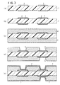
- the multilayer printed wiring board according to the fourth embodiment is manufactured as will be described herebelow with reference to FIGS. 3 and 4.
- the manufacturing process is substantially same as that for the first embodiment and thus includes the previously mentioned steps (1) to (14).
- a composite of fluororesin and heat-resistant thermoplastic resin, composite of fluororesin and thermosetting resin or a composite of thermosetting and thermoplastic resins is used as the interlaminar insulative resin layer.
- an electroless plating adhesive using the composite as resin matrix should preferably be used.
- the hole for the viahole is formed by exposing, developing and then thermally curing the resin layer.
- the resin is a composite of fluororesin and heat-resistant thermoplastic resin, composite of fluororesin and thermosetting resin or a composite of thermosetting and thermoplastic resins
- the hole for the viahole is formed by thermosetting the resin layer and then by lasing drilling.
- the ratio D/T 1 between the viahole diameter (D) and interlaminar insulative resin layer thickness (T 1 ) should preferably be within a range of 1 to 4. This is because if the ratio D/T 1 is less than 1, the electroplating solution will not enter the hole while the ratio over 4 will not allow the hole to sufficiently be filled with a plating metal.
- the surface of the interlaminar insulative resin layer should preferably be roughened by plasma etching or the like for this roughening will improve the adhesion to the plating layer.
- the epoxy resin particles existent on the surface of the cured adhesive layer are removed by decomposing or dissolving with an acid or oxidant to rough the surface of the adhesive layer.
- examples 1 to 9 and comparative examples 1 to 8 of multilayer printed wiring boards were prepared through the steps (1) to (11) of the 14 steps having been described in the foregoing, not yet including the step at which the solder bump is formed.
- Example 11 was prepared through all the steps (1) to (14). The multilayer printed wiring boards thus prepared will further be described in detail herebelow:
- a multilayer printed wiring board was prepared in the same manner as the aforementioned example 1 except that an interlaminar insulative resin layer was formed by attaching a fluororesin film of 20 ⁇ m in thickness to the layer by thermo-compression bonding and holes for viaholes of 60 ⁇ m in diameter were formed by irradiating ultraviolet laser.
- a multilayer printed wiring board was produced in the same manner as the aforementioned example 1 except that a conductor circuit was made only of an electroless plating layer of 25 ⁇ m in thickness and viaholes were formed by dipping for 11 hours in en electroless plating aqueous solution composed of 0.06 mol/l of copper sulfide, 0.3 mol/l of formalin, 0.35 mol/l of NaOH, 0.35 mol/l of EDTA and a small amount of additive at 75°C and having a pH of 12.4.
- the holes in the interlaminar insulative resin layer were found filled with the plating layer, but a depression of 20 to 25 m was found in the central portion of the plating layer.
- a multilayer printed wiring board was produced. More particularly, the steps (1) to (5) for the embodiment 1 were repeated to process a substrate and then the substrate was dipped in an electroless plating solution prepared from an aqueous solution composed of 0.05 mol/l of copper sulfide, 0. 30 mol/l of formalin, 0. 35 mol/l of sodium hydroxide, and 0. 35 mol/l of ethylenediaminetetraacetic acid (EDTA) to formaplating layer of 40 ⁇ m in thickness.
- an electroless plating solution prepared from an aqueous solution composed of 0.05 mol/l of copper sulfide, 0. 30 mol/l of formalin, 0. 35 mol/l of sodium hydroxide, and 0. 35 mol/l of ethylenediaminetetraacetic acid (EDTA) to formaplating layer of 40 ⁇ m in thickness.
- etching resist 25/25 ⁇ m on the substrate.
- the substrate was dipped in a mixed solution of sulfuric acid and hydrogen peroxide.
- the conductor circuitry layer was undercut and separated. Therefore, the comparative example 2 was not evaluated.
- the examples 1 to 3 and comparative example 1 were evaluated as to 1 ⁇ surface flatness of their interlaminar insulative resin layer and 2 ⁇ electrical connection reliability of the viahole.
- the above item 1 ⁇ surface flatness, was evaluated by judging whether a depression developed on a first applied interlaminar insulative resin layer.
- the item 2 ⁇ electrical connection reliability of the viahole, was evaluated by checking, using a probe, whether a further viahole formed on a viahole already formed showed a poor electrical continuity. The evaluation results are shown in Table 1.
- the examples 1, 2 and 3 are superior in surface flatness of the interlaminar insulative resin layer. Even when the further viahole is provided on the inner one, a circuit pattern breaking due to a depression is not observed, namely, the examples Depression on interlaminar insulative resin layer Poor electrical continuity
- Example 1 No No Example 2 - No Example 3 - No Comparative example 1 Yes No 1 to 3 have a high electrical connection reliability of the viahole, and IC chip and other devices can easily be mounted on the wiring boards with no inconvenience. Further, even when mass-produced, the examples 1 to 3 will show a high electrical connection reliability of the viaholes.
- the first embodiment of the present invention provides a multilayer printed wiring board having a filled viahole structure enabling a fine circuit pattern to be formed and showing superior surface flatness and high electrical connection reliability of the viahole.
- a multilayer printed wiring board was produced by repeating the steps (1) to (5) for the example 1, and further processing the substrate as follows:
- a multilayer printed wiring board was produced by repeating the steps (1) to (3) for the example 3, and further processing the substrate as follows:
- a multilayer printed wiring board was produced. More particularly, the steps (1) to (5) for the embodiment 5 were repeated and then the substrate was dipped in an electroless plating solution prepared from an aqueous solution composed of 0.05 mol/l of copper sulfide, 0. 30 mol/l of formalin, 0. 35 mol/l of sodium hydroxide, and 0.35 mol/l of ethylenediaminetetraacetic acid (EDTA) to form a plating layer of 40 ⁇ m in thickness.
- an electroless plating solution prepared from an aqueous solution composed of 0.05 mol/l of copper sulfide, 0. 30 mol/l of formalin, 0. 35 mol/l of sodium hydroxide, and 0.35 mol/l of ethylenediaminetetraacetic acid (EDTA) to form a plating layer of 40 ⁇ m in thickness.
- EDTA ethylenediaminetetraacetic acid
- the substrate was dipped in a mixed solution of sulfuric acid and hydrogen peroxide.
- the conductor circuitry layer was undercut and separated.
- a multilayer printed wiring board was produced by repeating the steps (1) to (5) for the example 1, and further processing the substrate as follows:
- a multilayer printed wiring board was produced by repeating the steps (1) to (3) for the example 2, and further processing the substrate as follows:
- a multilayer printed wiring board was produced similarly to the embodiment as disclosed in the Japanese unexamined patent publication No. hei 2-188992.
- the holes for viaholes were filled only with the electroless plating layer to form the viaholes.
- a multilayer printed wiring board was produced by repeating the steps (1) to (3) for the example 6 and further processing the substrate as follows.
- the substrate was dipped in an electroless plating solution prepared from an aqueous solution composed of 0.05 mol/l of copper sulfide, 0. 30 mol/l of formalin, 0.35 mol/l of sodium hydroxide, and 0.35 mol/l of ethylenediaminetetraacetic acid (EDTA) to form a plating layer of 1 ⁇ m in thickness.
- an electroless plating solution prepared from an aqueous solution composed of 0.05 mol/l of copper sulfide, 0. 30 mol/l of formalin, 0.35 mol/l of sodium hydroxide, and 0.35 mol/l of ethylenediaminetetraacetic acid (EDTA) to form a plating layer of 1 ⁇ m in thickness.
- EDTA ethylenediaminetetraacetic acid
- this multilayer printed wiring board had no roughed surface on the viahole.
- the comparative example 5 showed a cracking in the viahole portion
- the comparative example 6 showed a separation of the viahole portion
- the examples 6 and 7 showed neither separation nor cracking at the viahole portion.
- the third embodiment of the present invention provides amultilayer printed wiring board having a filled viahole structure in which the viahole is not easily separable and no crack takes place under a thermal shock or due to heat cycle.
- a multilayer printed wiring board was produced of which the interlaminar insulative resin layer was made of a composite of fluororesin and heat-resistant thermoplastic resin, through a process including the following steps:
- a multilayer printed wiring board was produced of which the interlaminar insulative resin layer was made of a composite of fluororesin and thermosetting resin, by repeating the above steps (1) to (3) for the example 3 and further processing the substrate as follows:
- a multilayer printed wiring board of which the interlaminar insulative resin layer was made of a composite of thermosetting and thermoplastic resins was produced by repeating the steps (1) to (6) for the example 1 and further processing the substrate as follows:
- the viahole 10 had a flat surface, and the conductor surface was at a same level as the viahole surface.
- a multilayer printed wiring board was produced of which the interlaminar insulative resin layer was made only of a thermosetting resin, as follows:
- a multilayer printed wiring board was produced in the same manner as for the example 8 except that no leveling agent and brightening agent were added to the electroplating solution. As a result, a plating layer could not sufficiently be filled in the holes for the viaholes.
- the example 8 is highly resistant against violent temperature variation since its interlaminar insulative resin layer incorporates a fluororesin and thermoplastic resin.
- the fourth embodiment of the present invention provides a multilayer printed wiring board having a filled viahole structure permitting to positively prevent line breakage in the wiring board and improved in resistance against violent temperature variation.
- a multilayer printed wiring board was produced by repeating the steps (1) to (9) for the example 1, and further processing the substrate as follows:
- the viahole is not filled, a large amount of solder paste has to be used or the printing mask hole has to be large to form a solder bump as high as the solder bump of a flat solder pad.
- the solder paste can be applied uniformly and the hole in the printing mask may be uniform in size.
- the present invention provides a multilayer printed wiring board best suitable for forming a fine circuit pattern thereon, providing an excellent adhesion between the conductor circuit and interlaminar insulative resin layer and an outstanding resistance against cracking due to heat cycle.
- the multilayer printed wiring board according to the present invention has an excellent applicability in many fields of art requiring a high performance and high packaging density of electronic parts.
Landscapes
- Engineering & Computer Science (AREA)
- Manufacturing & Machinery (AREA)
- Microelectronics & Electronic Packaging (AREA)
- Production Of Multi-Layered Print Wiring Board (AREA)
- Manufacturing Of Printed Wiring (AREA)
- Printing Elements For Providing Electric Connections Between Printed Circuits (AREA)
Abstract
Description
As a result, the adhesion between the viahole and interlaminar insulative resin layer is improved. Also, since the electroplating layer having a larger malleability than the electroless plating layer fills the major part of the hole, the electroplating layer will flexibly follow the expansion and shrinkage of the interlaminar insulative resin layer, thus the layers can be prevented from being cracked under a thermal shock or due to heat cycle.
(A) In a multilayer printed wiring board having conductor circuitry layers and interlaminar insulative resin layers deposited alternately one on another and in which the interlaminar insulative resin layers have formed through them holes each filledwith a plating layer to formaviahole, according to the first embodiment of the present invention, the surface of the viahole formed from each hole filled with the plating layer is formed substantially flat and lies at a substantially same level as the surface of the conductor circuit later disposed in the interlaminar insulative resin layer in which the viahole also lies, and the thickness of the conductor circuitry layer is less than a half of the viahole diameter.
2Cu(I)An/2 + n/4O2 + nAH (aeration) → 2Cu(II)An + n/2H2O
| Aqueous electroplating solution: | |
| CuSO4·5H2O | 60 g/l |
| Leveling agent (HL by ATOTTECH) | 40 ml/l |
| Sulfuric acid | 190 g/l |
| Brightening agent (UV by ATOTTECH) | 0.5 ml/l |
| Chlorine ion | 40 ppm |
| Electroplating conditions: | |
| Bubbling | 3.0 liters/min |
| Current density | 0.5 A/dm2 |
| Set current value | 0.18 A |
| Plating length of time | 130 min |
| Depression on interlaminar insulative resin layer | Poor electrical continuity | ||
| Example 1 | No | No | |
| Example 2 | - | No | |
| Example 3 | - | No | |
| Comparative example 1 | | No |
| Aqueous electroplating solution: | |
| CuSO4·5H2O | 60 g/l |
| Leveling agent (HL by ATOTTECH) | 40 ml/l |
| Sulfuric acid | 190 g/l |
| Brightening agent (UV by ATOTTECH) | 0.5 ml/l |
| Chlorine ion | 40 ppm |
| Electroplating conditions: | |
| Bubbling | 3.0 liters/min |
| Current density | 0.5 A/dm2 |
| Set current value | 0.18 A |
| Plating length of time | 100 min |
| Separation of viahole | Cracking in viahole | |
| Example 6 | No | No |
| Example 7 | No | No |
| Comparative example 5 | No | Yes |
| Comparative example 6 | Yes | No |
| Aqueous electroplating solution: | |
| CuSO4·5H2O | 60 g/l |
| Leveling agent (HL by ATOTTECH) | 40 ml/l |
| Sulfuric acid | 190 g/l |
| Brightening agent (UV by ATOTTECH) | 0.5 ml/l |
| Chlorine ion | 40 ppm |
| Electroplating conditions: | |
| Bubbling | 3.0 liters/min |
| Current density | 0.5 A/dm2 |
| Set current value | 0.18 A |
| Plating length of time | 130 min |
| Crack starting at viahole | Separation or crack of plating layer | |||
| 500 heat cycles | 1000 heat cycles | 500 heat cycles | 1000 heat cycles | |
| Example 8 | No | No | No | No |
| Example 9 | No | No | No | No |
| Example 10 | No | Yes | No | No |
| Comparative example 7 | Yes | Yes | No | No |
| Comparative example 8 | No | No | Yes | Yes |
Claims (7)
- The multilayer printed wiring board having conductor circuit layers (2,12) and interlaminar insulative resin layers (4) deposited alternately one on another, the interlaminar insulative resin layers (4) each having formed through them holes (5) each filled with a plating layer (9) to form a filled viahole (10),
characterized in that
a thickness (T2) of said conductor circuit layer (2,12) is less than a half of the filled vehicle diameter (D) and less than 25 µm,
a depression is formed on a central surface portion of the plating layer (9) surface exposed out of the viahole (10), said depression having a size less than the thickness of the conductor circuit layer (2,12), and
the surface of the plating layer (9) and the surface of the conductor circuit layer (2,12) exposed out of the viahole (10) are roughened. - The multilayer printed wiring board according to claim 1, wherein the size of the depression is 20 µm or less.
- The multilayer printed wiring board as set forth in claim 1 or 2, wherein the inner wall of the hole (5) is roughened.
- The multilayer printed wiring board as set for in one of claims 1 to 3, wherein the surfaces (3) of the inner conductor circuits (2) connected to each other by the filled viahole are roughened.
- The multilayer printed wiring board as set forth in one of claims 1 to 4, wherein a further viahole (20) is formed on the filled viahole (10).
- The multilayer printed wiring board as set forth in one of claims 1 to 5, wherein the interlaminar insulative resin layer (4) in which the filled viaholes (10) are formed is made of a thermoplastic resin or a composite of thermoplastic and thermosetting resins.
- The multilayer printed wiring board as set forth in one of claims 1 to 6, wherein a ratio between the filled viahole diameter (D) and interlaminar insulative resin layer thickness (4,T1) is within a range of 1 to 4.
Applications Claiming Priority (9)
| Application Number | Priority Date | Filing Date | Title |
|---|---|---|---|
| JP4539898 | 1998-02-26 | ||
| JP10045399A JPH11243279A (en) | 1998-02-26 | 1998-02-26 | Multilayer printed wiring board having field via structure |
| JP10045397A JPH11243277A (en) | 1998-02-26 | 1998-02-26 | Multilayer printed wiring board having filled via structure |
| JP10045396A JPH11243280A (en) | 1998-02-26 | 1998-02-26 | Multilayer printed wiring board having filled via structure |
| JP4539698 | 1998-02-26 | ||
| JP10045398A JPH11243278A (en) | 1998-02-26 | 1998-02-26 | Multilayer printed wiring board having filled via structure |
| JP4539998 | 1998-02-26 | ||
| JP4539798 | 1998-02-26 | ||
| EP19990902842 EP1075172B1 (en) | 1998-02-26 | 1999-02-05 | Multilayer printed wiring board having filled-via structure |
Related Parent Applications (1)
| Application Number | Title | Priority Date | Filing Date |
|---|---|---|---|
| EP19990902842 Division EP1075172B1 (en) | 1998-02-26 | 1999-02-05 | Multilayer printed wiring board having filled-via structure |
Publications (3)
| Publication Number | Publication Date |
|---|---|
| EP1505859A2 true EP1505859A2 (en) | 2005-02-09 |
| EP1505859A3 EP1505859A3 (en) | 2005-02-16 |
| EP1505859B1 EP1505859B1 (en) | 2007-08-15 |
Family
ID=27461693
Family Applications (4)
| Application Number | Title | Priority Date | Filing Date |
|---|---|---|---|
| EP19990902842 Expired - Lifetime EP1075172B1 (en) | 1998-02-26 | 1999-02-05 | Multilayer printed wiring board having filled-via structure |
| EP20070008979 Withdrawn EP1811825A1 (en) | 1998-02-26 | 1999-02-05 | Multilayer printed wiring board with filled viaholes |
| EP20040024664 Expired - Lifetime EP1505859B1 (en) | 1998-02-26 | 1999-02-05 | Multilayer printed wiring board having filled via-holes |
| EP20050012908 Expired - Lifetime EP1583407B1 (en) | 1998-02-26 | 1999-02-05 | Multilayer printed wiring board with filled viaholes |
Family Applications Before (2)
| Application Number | Title | Priority Date | Filing Date |
|---|---|---|---|
| EP19990902842 Expired - Lifetime EP1075172B1 (en) | 1998-02-26 | 1999-02-05 | Multilayer printed wiring board having filled-via structure |
| EP20070008979 Withdrawn EP1811825A1 (en) | 1998-02-26 | 1999-02-05 | Multilayer printed wiring board with filled viaholes |
Family Applications After (1)
| Application Number | Title | Priority Date | Filing Date |
|---|---|---|---|
| EP20050012908 Expired - Lifetime EP1583407B1 (en) | 1998-02-26 | 1999-02-05 | Multilayer printed wiring board with filled viaholes |
Country Status (8)
| Country | Link |
|---|---|
| US (6) | US7071424B1 (en) |
| EP (4) | EP1075172B1 (en) |
| KR (4) | KR20060095785A (en) |
| CN (2) | CN1168361C (en) |
| DE (3) | DE69928518T2 (en) |
| MY (1) | MY129801A (en) |
| TW (1) | TW404158B (en) |
| WO (1) | WO1999044403A1 (en) |
Families Citing this family (127)
| Publication number | Priority date | Publication date | Assignee | Title |
|---|---|---|---|---|
| DE69928518T2 (en) * | 1998-02-26 | 2006-03-30 | Ibiden Co., Ltd., Ogaki | MULTILAYER CONDUCTOR PLATE WITH A STRUCTURE OF FILLED CONTACT HOLES |
| EP2086300A1 (en) | 1999-06-02 | 2009-08-05 | Ibiden Co., Ltd. | Multi-layer printed circuit board and method of manufacturing multi-layer printed circuit board |
| US7514637B1 (en) | 1999-08-06 | 2009-04-07 | Ibiden Co., Ltd. | Electroplating solution, method for fabricating multilayer printed wiring board using the solution, and multilayer printed wiring board |
| JP4062907B2 (en) * | 2001-11-12 | 2008-03-19 | 松下電器産業株式会社 | Circuit board and manufacturing method thereof |
| JP4029759B2 (en) * | 2003-04-04 | 2008-01-09 | 株式会社デンソー | Multilayer circuit board and manufacturing method thereof |
| TW200521171A (en) | 2003-12-26 | 2005-07-01 | Toshiba Kk | Resin particles and resin layer containing metal micro particles, its forming method and circuit base board |
| JP4426900B2 (en) * | 2004-05-10 | 2010-03-03 | 三井金属鉱業株式会社 | Printed wiring board, manufacturing method thereof, and semiconductor device |
| US7626829B2 (en) | 2004-10-27 | 2009-12-01 | Ibiden Co., Ltd. | Multilayer printed wiring board and manufacturing method of the multilayer printed wiring board |
| KR100845534B1 (en) * | 2004-12-31 | 2008-07-10 | 엘지전자 주식회사 | Conductive Metal Plated Polyimide Substrate and Manufacturing Method Thereof |
| CN100423254C (en) * | 2005-02-14 | 2008-10-01 | 富士通株式会社 | Semiconductor device and method of manufacturing the same, and capacitor structure and method of manufacturing the same |
| KR100688864B1 (en) * | 2005-02-25 | 2007-03-02 | 삼성전기주식회사 | Printed Circuit Board, Flip Chip Ball Grid Array Substrate and Manufacturing Method Thereof |
| TWI261329B (en) * | 2005-03-09 | 2006-09-01 | Phoenix Prec Technology Corp | Conductive bump structure of circuit board and method for fabricating the same |
| US7701071B2 (en) * | 2005-03-24 | 2010-04-20 | Texas Instruments Incorporated | Method for fabricating flip-attached and underfilled semiconductor devices |
| JP4790297B2 (en) * | 2005-04-06 | 2011-10-12 | ルネサスエレクトロニクス株式会社 | Semiconductor device and manufacturing method thereof |
| US7650694B2 (en) * | 2005-06-30 | 2010-01-26 | Intel Corporation | Method for forming multilayer substrate |
| JP2007042666A (en) * | 2005-07-29 | 2007-02-15 | Victor Co Of Japan Ltd | Printed wiring board and its manufacturing method |
| US20070031758A1 (en) * | 2005-08-03 | 2007-02-08 | Jsr Corporation | Positive-type radiation-sensitive resin composition for producing a metal-plating formed material, transcription film and production method of a metal-plating formed material |
| IL171378A (en) | 2005-10-11 | 2010-11-30 | Dror Hurwitz | Integrated circuit support structures and the fabrication thereof |
| US7416923B2 (en) * | 2005-12-09 | 2008-08-26 | International Business Machines Corporation | Underfill film having thermally conductive sheet |
| JP2007173371A (en) * | 2005-12-20 | 2007-07-05 | Shinko Electric Ind Co Ltd | Method for manufacturing flexible wiring board and method for manufacturing electronic component mounting structure |
| US7906850B2 (en) * | 2005-12-20 | 2011-03-15 | Unimicron Technology Corp. | Structure of circuit board and method for fabricating same |
| DE102006028692B4 (en) * | 2006-05-19 | 2021-09-02 | OSRAM Opto Semiconductors Gesellschaft mit beschränkter Haftung | Electrically conductive connection with an insulating connection medium |
| KR100797692B1 (en) | 2006-06-20 | 2008-01-23 | 삼성전기주식회사 | Printed Circuit Board and Manufacturing Method |
| US7570082B2 (en) * | 2006-08-15 | 2009-08-04 | International Business Machines Corporation | Voltage comparator apparatus and method having improved kickback and jitter characteristics |
| WO2008053833A1 (en) * | 2006-11-03 | 2008-05-08 | Ibiden Co., Ltd. | Multilayer printed wiring board |
| JP5214139B2 (en) * | 2006-12-04 | 2013-06-19 | 新光電気工業株式会社 | Wiring board and manufacturing method thereof |
| CN101296570A (en) * | 2007-04-25 | 2008-10-29 | 富葵精密组件(深圳)有限公司 | Circuit board and manufacturing method thereof |
| US7969005B2 (en) * | 2007-04-27 | 2011-06-28 | Sanyo Electric Co., Ltd. | Packaging board, rewiring, roughened conductor for semiconductor module of a portable device, and manufacturing method therefor |
| JP2009010276A (en) * | 2007-06-29 | 2009-01-15 | C Uyemura & Co Ltd | Wiring board manufacturing method |
| KR100811620B1 (en) | 2007-07-02 | 2008-03-07 | 에스티주식회사 | Manufacturing method of printed circuit board |
| US8192815B2 (en) | 2007-07-13 | 2012-06-05 | Apple Inc. | Methods and systems for forming a dual layer housing |
| TWI358981B (en) * | 2007-08-08 | 2012-02-21 | Unimicron Technology Corp | Method for fabricating circuit board |
| CN101409982B (en) * | 2007-10-09 | 2010-06-16 | 南亚电路板股份有限公司 | Manufacturing method of circuit board |
| JP2009099589A (en) * | 2007-10-12 | 2009-05-07 | Elpida Memory Inc | Wafer or circuit board and connection structure thereof |
| USPP19906P2 (en) * | 2007-10-31 | 2009-04-14 | Tai-Ling Biotech Inc. | Phalaenopsis plant named ‘Queen V6’ |
| US8309856B2 (en) * | 2007-11-06 | 2012-11-13 | Ibiden Co., Ltd. | Circuit board and manufacturing method thereof |
| TWI450666B (en) * | 2007-11-22 | 2014-08-21 | Ajinomoto Kk | Production method of multilayer printed wiring board and multilayer printed wiring board |
| KR20090067249A (en) * | 2007-12-21 | 2009-06-25 | 삼성전기주식회사 | Printed Circuit Board and Manufacturing Method |
| US8315043B2 (en) * | 2008-01-24 | 2012-11-20 | Apple Inc. | Methods and systems for forming housings from multi-layer materials |
| JP2009182272A (en) * | 2008-01-31 | 2009-08-13 | Sanyo Electric Co Ltd | Device mounting substrate and manufacturing method thereof, semiconductor module and manufacturing method thereof, and portable device |
| JP2009231596A (en) * | 2008-03-24 | 2009-10-08 | Fujitsu Ltd | Multilayer wiring board, multilayer wiring board unit, and electronic device |
| US8646637B2 (en) * | 2008-04-18 | 2014-02-11 | Apple Inc. | Perforated substrates for forming housings |
| US8367304B2 (en) * | 2008-06-08 | 2013-02-05 | Apple Inc. | Techniques for marking product housings |
| KR100962369B1 (en) * | 2008-06-26 | 2010-06-10 | 삼성전기주식회사 | Printed circuit board and manufacturing method thereof |
| KR100999918B1 (en) * | 2008-09-08 | 2010-12-13 | 삼성전기주식회사 | Printed Circuit Board and Manufacturing Method Thereof |
| JP5203108B2 (en) | 2008-09-12 | 2013-06-05 | 新光電気工業株式会社 | Wiring board and manufacturing method thereof |
| CN102573268B (en) * | 2008-09-30 | 2015-03-11 | 揖斐电株式会社 | Multilayer printed wiring board and method for manufacturing multilayer printed wiring board |
| US20100159273A1 (en) | 2008-12-24 | 2010-06-24 | John Benjamin Filson | Method and Apparatus for Forming a Layered Metal Structure with an Anodized Surface |
| FR2940879B1 (en) * | 2009-01-06 | 2012-12-21 | Thales Sa | METHOD OF MAKING A PRINTED BOARD AND CORRESPONDING PRINTED BOARD |
| CN101790288B (en) * | 2009-01-22 | 2012-08-29 | 上海美维科技有限公司 | Manufacturing method of novel printed circuit board |
| US9173336B2 (en) | 2009-05-19 | 2015-10-27 | Apple Inc. | Techniques for marking product housings |
| US9884342B2 (en) | 2009-05-19 | 2018-02-06 | Apple Inc. | Techniques for marking product housings |
| US9627254B2 (en) * | 2009-07-02 | 2017-04-18 | Flipchip International, Llc | Method for building vertical pillar interconnect |
| US8426959B2 (en) * | 2009-08-19 | 2013-04-23 | Samsung Electronics Co., Ltd. | Semiconductor package and method of manufacturing the same |
| US8663806B2 (en) | 2009-08-25 | 2014-03-04 | Apple Inc. | Techniques for marking a substrate using a physical vapor deposition material |
| EP2461659A4 (en) * | 2009-09-02 | 2014-08-20 | Panasonic Corp | PRINTED CIRCUIT BOARD, ASSEMBLED MULTILAYER BOARD, AND PRODUCTION METHOD |
| US10071583B2 (en) | 2009-10-16 | 2018-09-11 | Apple Inc. | Marking of product housings |
| US9845546B2 (en) | 2009-10-16 | 2017-12-19 | Apple Inc. | Sub-surface marking of product housings |
| US8809733B2 (en) | 2009-10-16 | 2014-08-19 | Apple Inc. | Sub-surface marking of product housings |
| US8067266B2 (en) * | 2009-12-23 | 2011-11-29 | Intel Corporation | Methods for the fabrication of microelectronic device substrates by attaching two cores together during fabrication |
| CN102118925A (en) * | 2009-12-30 | 2011-07-06 | 深圳富泰宏精密工业有限公司 | Shell of electronic device and manufacturing method thereof |
| JP5603600B2 (en) * | 2010-01-13 | 2014-10-08 | 新光電気工業株式会社 | WIRING BOARD, MANUFACTURING METHOD THEREOF, AND SEMICONDUCTOR PACKAGE |
| US8628836B2 (en) | 2010-03-02 | 2014-01-14 | Apple Inc. | Method and apparatus for bonding metals and composites |
| TW201132246A (en) * | 2010-03-09 | 2011-09-16 | Nan Ya Printed Circuit Board | Side packaged type printed circuit board |
| JP5638269B2 (en) * | 2010-03-26 | 2014-12-10 | 日本特殊陶業株式会社 | Multilayer wiring board |
| US8489158B2 (en) | 2010-04-19 | 2013-07-16 | Apple Inc. | Techniques for marking translucent product housings |
| TWI381780B (en) * | 2010-04-28 | 2013-01-01 | Wus Printed Circuit Co Ltd | Manufacturing method for identifiable pcb |
| US8724285B2 (en) | 2010-09-30 | 2014-05-13 | Apple Inc. | Cosmetic conductive laser etching |
| US8901431B2 (en) * | 2010-12-16 | 2014-12-02 | Ibiden Co., Ltd. | Printed wiring board and method for manufacturing printed wiring board |
| US8569861B2 (en) * | 2010-12-22 | 2013-10-29 | Analog Devices, Inc. | Vertically integrated systems |
| JP2012182437A (en) * | 2011-02-09 | 2012-09-20 | Ngk Spark Plug Co Ltd | Wiring board and method of manufacturing the same |
| JP5675443B2 (en) * | 2011-03-04 | 2015-02-25 | 新光電気工業株式会社 | Wiring board and method of manufacturing wiring board |
| US20120248001A1 (en) | 2011-03-29 | 2012-10-04 | Nashner Michael S | Marking of Fabric Carrying Case for Portable Electronic Device |
| US9280183B2 (en) | 2011-04-01 | 2016-03-08 | Apple Inc. | Advanced techniques for bonding metal to plastic |
| DE102011006899B4 (en) | 2011-04-06 | 2025-01-30 | Te Connectivity Germany Gmbh | Method for producing contact elements by mechanical application of material layer with high resolution as well as contact element and a device for producing |
| US20120286416A1 (en) * | 2011-05-11 | 2012-11-15 | Tessera Research Llc | Semiconductor chip package assembly and method for making same |
| US8879266B2 (en) * | 2012-05-24 | 2014-11-04 | Apple Inc. | Thin multi-layered structures providing rigidity and conductivity |
| US10071584B2 (en) | 2012-07-09 | 2018-09-11 | Apple Inc. | Process for creating sub-surface marking on plastic parts |
| KR101506785B1 (en) * | 2013-05-29 | 2015-03-27 | 삼성전기주식회사 | Printed Circuit Board |
| US9434197B2 (en) | 2013-06-18 | 2016-09-06 | Apple Inc. | Laser engraved reflective surface structures |
| US9314871B2 (en) | 2013-06-18 | 2016-04-19 | Apple Inc. | Method for laser engraved reflective surface structures |
| US11268526B2 (en) | 2013-07-09 | 2022-03-08 | Raytheon Technologies Corporation | Plated polymer fan |
| US11691388B2 (en) | 2013-07-09 | 2023-07-04 | Raytheon Technologies Corporation | Metal-encapsulated polymeric article |
| EP3019723A4 (en) | 2013-07-09 | 2017-05-10 | United Technologies Corporation | Plated polymer compressor |
| CA2917916A1 (en) | 2013-07-09 | 2015-02-05 | United Technologies Corporation | Plated polymer nosecone |
| KR101483875B1 (en) * | 2013-07-31 | 2015-01-16 | 삼성전기주식회사 | Glass core substrate and manufacturing method thereof |
| TWM470379U (en) * | 2013-09-05 | 2014-01-11 | 思鷺科技股份有限公司 | Ceramic circuit board and LED package module having the same |
| CN103732011B (en) * | 2013-12-24 | 2016-06-08 | 广州兴森快捷电路科技有限公司 | The manufacture method of printed wiring board blind hole |
| US9398703B2 (en) * | 2014-05-19 | 2016-07-19 | Sierra Circuits, Inc. | Via in a printed circuit board |
| JP2015222753A (en) * | 2014-05-22 | 2015-12-10 | イビデン株式会社 | Printed wiring board and method for manufacturing the same |
| KR102412612B1 (en) * | 2015-08-28 | 2022-06-23 | 삼성전자주식회사 | board for package and prepreg |
| US20170064821A1 (en) * | 2015-08-31 | 2017-03-02 | Kristof Darmawikarta | Electronic package and method forming an electrical package |
| KR20170038535A (en) * | 2015-09-30 | 2017-04-07 | 삼성전기주식회사 | Printed circuit board and manufacturing method of the same |
| KR102546379B1 (en) * | 2015-10-22 | 2023-06-21 | 에이지씨 가부시키가이샤 | Manufacturing method of wiring board |
| TWI574595B (en) | 2015-10-28 | 2017-03-11 | 財團法人工業技術研究院 | Manufacturing method for multilayer wiring and multilayer wiring structure |
| US9633924B1 (en) | 2015-12-16 | 2017-04-25 | Taiwan Semiconductor Manufacturing Company, Ltd. | Package structure and method for forming the same |
| US10177131B2 (en) | 2016-03-02 | 2019-01-08 | Samsung Electronics Co., Ltd. | Semiconductor packages and methods of manufacturing the same |
| JP2017191894A (en) * | 2016-04-14 | 2017-10-19 | イビデン株式会社 | Printed wiring board and manufacturing method of the same |
| JP2017199803A (en) * | 2016-04-27 | 2017-11-02 | 日立マクセル株式会社 | 3D molded circuit components |
| WO2017212742A1 (en) | 2016-06-09 | 2017-12-14 | 株式会社村田製作所 | Elastic wave device |
| KR20190043536A (en) * | 2016-09-01 | 2019-04-26 | 에이지씨 가부시키가이샤 | Wiring board and manufacturing method thereof |
| CN106535506A (en) * | 2016-12-15 | 2017-03-22 | 泰和电路科技(惠州)有限公司 | Via hole filling method, welding pad manufacturing method, welding pad and circuit board |
| US10163847B2 (en) * | 2017-03-03 | 2018-12-25 | Tdk Corporation | Method for producing semiconductor package |
| JP6894289B2 (en) * | 2017-05-17 | 2021-06-30 | 新光電気工業株式会社 | Wiring board and its manufacturing method |
| WO2019005116A1 (en) * | 2017-06-30 | 2019-01-03 | Manepalli Rahul N | Semiconductor package and method of making |
| TWI658767B (en) | 2017-09-28 | 2019-05-01 | Unimicron Technology Corp. | Circuit board manufacturing method and stack structure applied thereto |
| CN109600928B (en) * | 2017-09-30 | 2021-04-02 | 欣兴电子股份有限公司 | Manufacturing method of circuit board and stack structure applied to manufacture the same |
| US10827624B2 (en) * | 2018-03-05 | 2020-11-03 | Catlam, Llc | Catalytic laminate with conductive traces formed during lamination |
| KR20190130749A (en) | 2018-05-15 | 2019-11-25 | 정지성 | Commercial athletic goods dryer and drying method using it |
| US10506712B1 (en) * | 2018-07-31 | 2019-12-10 | Taiwan Semiconductor Manufacturing Co., Ltd. | Printed circuit board |
| US10999917B2 (en) | 2018-09-20 | 2021-05-04 | Apple Inc. | Sparse laser etch anodized surface for cosmetic grounding |
| US11829211B2 (en) * | 2018-09-28 | 2023-11-28 | Sharp Kabushiki Kaisha | Display device |
| KR102124324B1 (en) * | 2018-11-14 | 2020-06-18 | 와이엠티 주식회사 | Plating laminate and printed circuit board |
| KR102724892B1 (en) | 2018-12-04 | 2024-11-01 | 삼성전기주식회사 | Printed Circuit Board and manufacturing method for the same |
| US11039540B2 (en) * | 2019-01-01 | 2021-06-15 | Catlam, Llc | Multi-layer circuit board with traces thicker than a circuit board layer |
| TWI706705B (en) * | 2019-06-21 | 2020-10-01 | 唐虞企業股份有限公司 | Circuit board and manufacturing method thereof |
| KR102762871B1 (en) * | 2019-11-27 | 2025-02-07 | 삼성전기주식회사 | Printed circuit board |
| CN115336401A (en) * | 2020-03-30 | 2022-11-11 | 京瓷株式会社 | Printed wiring board and method for manufacturing printed wiring board |
| US11824031B2 (en) * | 2020-06-10 | 2023-11-21 | Advanced Semiconductor Engineering, Inc. | Semiconductor package structure with dielectric structure covering upper surface of chip |
| US11996357B2 (en) * | 2020-09-09 | 2024-05-28 | Ibiden Co., Ltd. | Wiring substrate and method for manufacturing wiring substrate |
| KR20220039071A (en) * | 2020-09-21 | 2022-03-29 | 삼성전기주식회사 | Electronic element module and printed circuit board for the same |
| KR20230054466A (en) * | 2020-09-28 | 2023-04-24 | 교세라 가부시키가이샤 | wiring board |
| CN113141703A (en) * | 2021-05-28 | 2021-07-20 | 四会富仕电子科技股份有限公司 | Metal-based rigid-flex board and production method thereof |
| US11991837B2 (en) * | 2021-06-22 | 2024-05-21 | Unimicron Technology Corp. | Circuit board and manufacturing method thereof |
| JP7768696B2 (en) * | 2021-07-21 | 2025-11-12 | マクセル株式会社 | Decorative plated products |
| US12324114B2 (en) | 2021-09-24 | 2025-06-03 | Apple Inc. | Laser-marked electronic device housings |
| CN114293056B (en) * | 2021-12-20 | 2022-12-23 | 富联裕展科技(深圳)有限公司 | Metal workpiece, metal product, etching solution and method for manufacturing metal workpiece |
Family Cites Families (86)
| Publication number | Priority date | Publication date | Assignee | Title |
|---|---|---|---|---|
| US3350498A (en) * | 1965-01-04 | 1967-10-31 | Intellux Inc | Multilayer circuit and method of making the same |
| US3536546A (en) * | 1968-10-07 | 1970-10-27 | North American Rockwell | Method of improving adhesion of copperepoxy glass laminates |
| JPS5516394B2 (en) * | 1973-01-11 | 1980-05-01 | ||
| JPS56100497A (en) | 1980-01-11 | 1981-08-12 | Mitsumi Electric Co Ltd | Ceramic circuit board |
| JPS5851436B2 (en) * | 1980-02-29 | 1983-11-16 | 株式会社東芝 | Printed circuit board manufacturing method |
| US4680220A (en) | 1985-02-26 | 1987-07-14 | W. L. Gore & Associates, Inc. | Dielectric materials |
| US4747897A (en) | 1985-02-26 | 1988-05-31 | W. L. Gore & Associates, Inc. | Dielectric materials |
| US4715894A (en) * | 1985-08-29 | 1987-12-29 | Techno Instruments Investments 1983 Ltd. | Use of immersion tin and tin alloys as a bonding medium for multilayer circuits |
| JPS62251136A (en) * | 1986-04-25 | 1987-10-31 | 三菱樹脂株式会社 | metal composite laminate |
| JPS62256496A (en) | 1986-04-30 | 1987-11-09 | 株式会社日立製作所 | Multilayer wiring board manufacturing method |
| JPH07105577B2 (en) | 1986-06-02 | 1995-11-13 | ジヤパンゴアテツクス株式会社 | Printed wiring board manufacturing method |
| DE3873896T2 (en) | 1987-12-23 | 1993-02-04 | Mitsubishi Gas Chemical Co | LAMINATING MATERIAL FOR PRINTED CIRCUIT BOARD WITH LOW DIELECTRICITY CONSTANT. |
| JPH0632386B2 (en) | 1988-01-19 | 1994-04-27 | イビデン株式会社 | Multilayer printed wiring board and manufacturing method thereof |
| DE3913966B4 (en) * | 1988-04-28 | 2005-06-02 | Ibiden Co., Ltd., Ogaki | Adhesive dispersion for electroless plating, and use for producing a printed circuit |
| JPH0254599A (en) | 1988-08-18 | 1990-02-23 | Fujitsu Ltd | Manufacture of multilayer printed board |
| MY104191A (en) | 1988-09-06 | 1994-02-28 | Mitsubishi Gas Chemical Co | Process for producing multilayer printed wiring board |
| JPH0734505B2 (en) | 1989-01-18 | 1995-04-12 | イビデン株式会社 | Multilayer printed wiring board and manufacturing method thereof |
| JP2776886B2 (en) | 1989-05-31 | 1998-07-16 | イビデン株式会社 | Multilayer printed wiring board and method of manufacturing the same |
| JP3069356B2 (en) | 1989-05-31 | 2000-07-24 | イビデン株式会社 | Multilayer printed wiring board and method of manufacturing the same |
| JPH06101627B2 (en) | 1989-10-04 | 1994-12-12 | 日本電気株式会社 | Multilayer printed wiring board and manufacturing method thereof |
| JP2688446B2 (en) * | 1990-03-26 | 1997-12-10 | 株式会社日立製作所 | Multilayer wiring board and manufacturing method thereof |
| JP2621634B2 (en) | 1990-10-24 | 1997-06-18 | 日本電気株式会社 | Manufacturing method of polyimide resin multilayer wiring board |
| US5103293A (en) | 1990-12-07 | 1992-04-07 | International Business Machines Corporation | Electronic circuit packages with tear resistant organic cores |
| JPH053388A (en) | 1991-06-25 | 1993-01-08 | Fujitsu Ltd | Method for manufacturing multilayer printed circuit board and insulating layer for multilayer printed circuit board |
| JPH0590761A (en) * | 1991-09-25 | 1993-04-09 | Hitachi Ltd | Wiring board manufacturing method |
| JPH05218646A (en) | 1992-02-05 | 1993-08-27 | Ngk Insulators Ltd | Manufacture of thin multilayer wiring board |
| JPH05218645A (en) | 1992-02-05 | 1993-08-27 | Ngk Insulators Ltd | Manufacture of thin multilayer wiring board |
| JP3204545B2 (en) | 1992-08-20 | 2001-09-04 | イビデン株式会社 | Multilayer printed wiring board and method of manufacturing the same |
| JPH06196856A (en) | 1992-09-29 | 1994-07-15 | Matsushita Electric Ind Co Ltd | Plating method, manufacture of multilayer printed-wiring board using this method and multilayer printed-wiring board |
| US5406034A (en) * | 1992-12-21 | 1995-04-11 | Motorola, Inc. | Circuit board having stepped vias |
| JPH06244556A (en) | 1993-02-19 | 1994-09-02 | Mitsubishi Gas Chem Co Inc | Manufacturing method of multilayer printed wiring board |
| JP2790956B2 (en) * | 1993-03-03 | 1998-08-27 | 株式会社日立製作所 | Manufacturing method of multilayer wiring board |
| US5600103A (en) * | 1993-04-16 | 1997-02-04 | Kabushiki Kaisha Toshiba | Circuit devices and fabrication method of the same |
| JPH06310856A (en) | 1993-04-26 | 1994-11-04 | Hitachi Kasei Ceramics Kk | Manufacture of multilayer wiring board |
| JP3290529B2 (en) | 1993-05-19 | 2002-06-10 | イビデン株式会社 | Adhesive for electroless plating, adhesive layer for electroless plating and printed wiring board |
| EP0629867B1 (en) * | 1993-06-16 | 1999-01-27 | Nitto Denko Corporation | Probe structure |
| JPH0745948A (en) | 1993-07-28 | 1995-02-14 | Ibiden Co Ltd | Multilayer wiring board and its manufacture |
| JPH0779078A (en) | 1993-09-08 | 1995-03-20 | Shinko Electric Ind Co Ltd | Multilayer wiring board and manufacturing method thereof |
| JPH07147483A (en) | 1993-09-30 | 1995-06-06 | Ibiden Co Ltd | Printed wiring board and manufacture thereof |
| JP3527766B2 (en) | 1993-11-30 | 2004-05-17 | 京セラ株式会社 | Manufacturing method of laminated circuit board and laminated circuit board |
| JP2694802B2 (en) * | 1993-12-28 | 1997-12-24 | 日本電気株式会社 | Manufacturing method of printed wiring board |
| JPH07235768A (en) | 1994-02-25 | 1995-09-05 | Toshiba Corp | Method for manufacturing thin film multilayer wiring board |
| JP3602565B2 (en) | 1994-03-04 | 2004-12-15 | イビデン株式会社 | Multilayer printed wiring board mounting IC chip and method of manufacturing multilayer printed wiring board therefor |
| JPH07283538A (en) | 1994-04-14 | 1995-10-27 | Ibiden Co Ltd | Manufacture of multilayered printed wiring board |
| JPH07283539A (en) | 1994-04-14 | 1995-10-27 | Sony Corp | Build-up multilayer printed wiring board |
| JPH07336017A (en) | 1994-06-08 | 1995-12-22 | Hitachi Ltd | Method of manufacturing thin film circuit by current reversal electrolysis method, thin film circuit board using the same, thin film multilayer circuit board and electronic circuit device |
| JPH0818239A (en) * | 1994-07-04 | 1996-01-19 | Hitachi Ltd | Manufacturing method of multilayer printed wiring board |
| US5652055A (en) | 1994-07-20 | 1997-07-29 | W. L. Gore & Associates, Inc. | Matched low dielectric constant, dimensionally stable adhesive sheet |
| JPH0846079A (en) | 1994-07-28 | 1996-02-16 | Matsushita Electric Ind Co Ltd | Semiconductor device |
| JPH08139452A (en) | 1994-11-14 | 1996-05-31 | Hitachi Ltd | Method for manufacturing multilayer wiring board |
| US5509200A (en) * | 1994-11-21 | 1996-04-23 | International Business Machines Corporation | Method of making laminar stackable circuit board structure |
| US5745333A (en) * | 1994-11-21 | 1998-04-28 | International Business Machines Corporation | Laminar stackable circuit board structure with capacitor |
| US5827604A (en) * | 1994-12-01 | 1998-10-27 | Ibiden Co., Ltd. | Multilayer printed circuit board and method of producing the same |
| JP3290041B2 (en) * | 1995-02-17 | 2002-06-10 | インターナショナル・ビジネス・マシーンズ・コーポレーション | Multilayer printed circuit board, method for manufacturing multilayer printed circuit board |
| JPH08250857A (en) | 1995-03-07 | 1996-09-27 | Murata Mfg Co Ltd | Manufacture of multilayer interconnection board |
| TW323432B (en) * | 1995-04-28 | 1997-12-21 | Victor Company Of Japan | |
| US6294743B1 (en) * | 1995-04-28 | 2001-09-25 | Victor Company Of Japan, Ltd. | Multilayer print circuit board and the production method of the multilayer print circuit board |
| US5816478A (en) * | 1995-06-05 | 1998-10-06 | Motorola, Inc. | Fluxless flip-chip bond and a method for making |
| KR100307776B1 (en) * | 1995-06-06 | 2001-11-22 | 엔도 마사루 | Printed circuit boards |
| US6444919B1 (en) * | 1995-06-07 | 2002-09-03 | International Business Machines Corporation | Thin film wiring scheme utilizing inter-chip site surface wiring |
| KR970004029A (en) | 1995-06-12 | 1997-01-29 | 김주용 | Method for forming charge storage electrode in semiconductor device manufacturing |
| JPH098458A (en) | 1995-06-16 | 1997-01-10 | Mitsubishi Electric Corp | Printed wiring board and manufacturing method thereof |
| JP3112059B2 (en) | 1995-07-05 | 2000-11-27 | 株式会社日立製作所 | Thin film multilayer wiring board and method of manufacturing the same |
| JPH09116273A (en) * | 1995-08-11 | 1997-05-02 | Shinko Electric Ind Co Ltd | Multilayer circuit board and method of manufacturing the same |
| JPH0983138A (en) * | 1995-09-07 | 1997-03-28 | Nippon Polytec Kk | Method of manufacturing multi-layered printed wiring board |
| US5699613A (en) * | 1995-09-25 | 1997-12-23 | International Business Machines Corporation | Fine dimension stacked vias for a multiple layer circuit board structure |
| JP3261314B2 (en) | 1995-11-10 | 2002-02-25 | イビデン株式会社 | Method of manufacturing multilayer printed wiring board and multilayer printed wiring board |
| JPH09214141A (en) | 1995-11-29 | 1997-08-15 | Nec Corp | Wiring construction |
| JPH09214140A (en) | 1995-11-29 | 1997-08-15 | Toppan Printing Co Ltd | Multilayer printed wiring board and method of manufacturing the same |
| JP3202936B2 (en) | 1996-03-04 | 2001-08-27 | イビデン株式会社 | Multilayer printed wiring board |
| JPH09266375A (en) | 1996-03-27 | 1997-10-07 | Ibiden Co Ltd | Multilayer printed interconnection board manufacturing method |
| JPH09307239A (en) | 1996-05-10 | 1997-11-28 | Matsushita Electric Works Ltd | Manufacture of multilayer printed wiring board |
| JPH09312472A (en) * | 1996-05-23 | 1997-12-02 | Kyocera Corp | Multilayer wiring board and method of manufacturing the same |
| JPH09331140A (en) | 1996-06-07 | 1997-12-22 | Ibiden Co Ltd | Manufacture of printed-wiring board |
| JPH104254A (en) | 1996-06-14 | 1998-01-06 | Ibiden Co Ltd | Method of manufacturing printed wiring board |
| JP3050807B2 (en) | 1996-06-19 | 2000-06-12 | イビデン株式会社 | Multilayer printed wiring board |
| JPH1046119A (en) * | 1996-08-08 | 1998-02-17 | Hitachi Chem Co Ltd | Pressure-sensitive adhesive film used in production of ivh-containing multilayer wiring board |
| US5830374A (en) * | 1996-09-05 | 1998-11-03 | International Business Machines Corporation | Method for producing multi-layer circuit board and resulting article of manufacture |
| US6162997A (en) * | 1997-06-03 | 2000-12-19 | International Business Machines Corporation | Circuit board with primary and secondary through holes |
| WO1999034654A1 (en) * | 1997-12-29 | 1999-07-08 | Ibiden Co., Ltd. | Multilayer printed wiring board |
| DE69928518T2 (en) * | 1998-02-26 | 2006-03-30 | Ibiden Co., Ltd., Ogaki | MULTILAYER CONDUCTOR PLATE WITH A STRUCTURE OF FILLED CONTACT HOLES |
| US6762921B1 (en) * | 1999-05-13 | 2004-07-13 | Ibiden Co., Ltd. | Multilayer printed-circuit board and method of manufacture |
| EP2086300A1 (en) * | 1999-06-02 | 2009-08-05 | Ibiden Co., Ltd. | Multi-layer printed circuit board and method of manufacturing multi-layer printed circuit board |
| WO2001019149A1 (en) * | 1999-09-02 | 2001-03-15 | Ibiden Co., Ltd. | Printed wiring board and method of producing the same and capacitor to be contained in printed wiring board |
| KR100890475B1 (en) * | 1999-09-02 | 2009-03-26 | 이비덴 가부시키가이샤 | Printed circuit board and method of manufacturing printed circuit board |
| TW512653B (en) * | 1999-11-26 | 2002-12-01 | Ibiden Co Ltd | Multilayer circuit board and semiconductor device |
-
1999
- 1999-02-05 DE DE1999628518 patent/DE69928518T2/en not_active Expired - Lifetime
- 1999-02-05 WO PCT/JP1999/000504 patent/WO1999044403A1/en not_active Ceased
- 1999-02-05 EP EP19990902842 patent/EP1075172B1/en not_active Expired - Lifetime
- 1999-02-05 US US09/600,890 patent/US7071424B1/en not_active Expired - Lifetime
- 1999-02-05 EP EP20070008979 patent/EP1811825A1/en not_active Withdrawn
- 1999-02-05 EP EP20040024664 patent/EP1505859B1/en not_active Expired - Lifetime
- 1999-02-05 KR KR1020067015985A patent/KR20060095785A/en not_active Ceased
- 1999-02-05 CN CNB99804394XA patent/CN1168361C/en not_active Expired - Lifetime
- 1999-02-05 CN CNB2004100560029A patent/CN100475005C/en not_active Expired - Lifetime
- 1999-02-05 DE DE1999636892 patent/DE69936892T2/en not_active Expired - Lifetime
- 1999-02-05 KR KR1020087014200A patent/KR100906931B1/en not_active Expired - Lifetime
- 1999-02-05 DE DE1999636235 patent/DE69936235T2/en not_active Expired - Lifetime
- 1999-02-05 KR KR1020087003146A patent/KR20080017496A/en not_active Ceased
- 1999-02-05 KR KR1020007009363A patent/KR100633678B1/en not_active Expired - Lifetime
- 1999-02-05 EP EP20050012908 patent/EP1583407B1/en not_active Expired - Lifetime
- 1999-02-25 MY MYPI99000690A patent/MY129801A/en unknown
- 1999-02-25 TW TW88102855A patent/TW404158B/en not_active IP Right Cessation
-
2004
- 2004-12-23 US US11/020,035 patent/US7390974B2/en not_active Expired - Fee Related
-
2006
- 2006-03-22 US US11/385,904 patent/US7622183B2/en not_active Expired - Fee Related
-
2008
- 2008-06-30 US US12/164,710 patent/US7737366B2/en not_active Expired - Fee Related
-
2009
- 2009-12-23 US US12/646,517 patent/US8115111B2/en not_active Expired - Fee Related
-
2012
- 2012-01-12 US US13/348,708 patent/US8987603B2/en not_active Expired - Fee Related
Also Published As
Similar Documents
| Publication | Publication Date | Title |
|---|---|---|
| EP1075172B1 (en) | Multilayer printed wiring board having filled-via structure | |
| EP1156525A1 (en) | Multilayer circuit board and semiconductor device | |
| US20100006334A1 (en) | Printed wiring board and method for manufacturing the same | |
| JP4511626B2 (en) | Manufacturing method of multilayer printed wiring board | |
| KR100629400B1 (en) | Multilayer printed wiring board | |
| JP4592889B2 (en) | Multilayer circuit board | |
| JP4592890B2 (en) | Multilayer circuit board | |
| JPH11243279A (en) | Multilayer printed wiring board having field via structure | |
| JPH11243280A (en) | Multilayer printed wiring board having filled via structure | |
| JPH11243277A (en) | Multilayer printed wiring board having filled via structure | |
| JP4812065B2 (en) | Multilayer printed wiring board having fill via structure | |
| JPH11243278A (en) | Multilayer printed wiring board having filled via structure | |
| JP4037534B2 (en) | Printed wiring board and manufacturing method thereof | |
| JP2003179358A (en) | Multilayer printed-wiring board with filled via structure | |
| JP2009038390A (en) | Method for manufacturing multilayer printed wiring board | |
| JP4875776B2 (en) | Method for manufacturing multilayer printed wiring board having fill via structure | |
| JP2009055059A (en) | Multi-layer printed wiring board having filled via structure | |
| JP2003179353A (en) | Multilayer printed-wiring board with filled via structure | |
| JP2003152339A (en) | Multilayer printed wiring board having filled-via structure |
Legal Events
| Date | Code | Title | Description |
|---|---|---|---|
| PUAI | Public reference made under article 153(3) epc to a published international application that has entered the european phase |
Free format text: ORIGINAL CODE: 0009012 |
|
| PUAL | Search report despatched |
Free format text: ORIGINAL CODE: 0009013 |
|
| 17P | Request for examination filed |
Effective date: 20041118 |
|
| AC | Divisional application: reference to earlier application |
Ref document number: 1075172 Country of ref document: EP Kind code of ref document: P |
|
| AK | Designated contracting states |
Kind code of ref document: A2 Designated state(s): DE FI GB NL |
|
| AK | Designated contracting states |
Kind code of ref document: A3 Designated state(s): DE FI GB NL |
|
| RIN1 | Information on inventor provided before grant (corrected) |
Inventor name: ASAI, MOTOOC/O IBIDEN CO., LTD., Inventor name: SHIRAI, SEIJIC/O IBIDEN CO., LTD., Inventor name: SHIMADA, KENICHIC/O IBIDEN CO., LTD., |
|
| 17Q | First examination report despatched |
Effective date: 20050503 |
|
| AKX | Designation fees paid |
Designated state(s): DE FI GB NL |
|
| GRAC | Information related to communication of intention to grant a patent modified |
Free format text: ORIGINAL CODE: EPIDOSCIGR1 |
|
| GRAP | Despatch of communication of intention to grant a patent |
Free format text: ORIGINAL CODE: EPIDOSNIGR1 |
|
| GRAS | Grant fee paid |
Free format text: ORIGINAL CODE: EPIDOSNIGR3 |
|
| GRAA | (expected) grant |
Free format text: ORIGINAL CODE: 0009210 |
|
| AC | Divisional application: reference to earlier application |
Ref document number: 1075172 Country of ref document: EP Kind code of ref document: P |
|
| AK | Designated contracting states |
Kind code of ref document: B1 Designated state(s): DE FI GB NL |
|
| REG | Reference to a national code |
Ref country code: GB Ref legal event code: FG4D |
|
| REF | Corresponds to: |
Ref document number: 69936892 Country of ref document: DE Date of ref document: 20070927 Kind code of ref document: P |
|
| PG25 | Lapsed in a contracting state [announced via postgrant information from national office to epo] |
Ref country code: FI Free format text: LAPSE BECAUSE OF FAILURE TO SUBMIT A TRANSLATION OF THE DESCRIPTION OR TO PAY THE FEE WITHIN THE PRESCRIBED TIME-LIMIT Effective date: 20070815 Ref country code: NL Free format text: LAPSE BECAUSE OF FAILURE TO SUBMIT A TRANSLATION OF THE DESCRIPTION OR TO PAY THE FEE WITHIN THE PRESCRIBED TIME-LIMIT Effective date: 20070815 |
|
| NLV1 | Nl: lapsed or annulled due to failure to fulfill the requirements of art. 29p and 29m of the patents act | ||
| PLBE | No opposition filed within time limit |
Free format text: ORIGINAL CODE: 0009261 |
|
| STAA | Information on the status of an ep patent application or granted ep patent |
Free format text: STATUS: NO OPPOSITION FILED WITHIN TIME LIMIT |
|
| 26N | No opposition filed |
Effective date: 20080516 |
|
| PGFP | Annual fee paid to national office [announced via postgrant information from national office to epo] |
Ref country code: GB Payment date: 20180131 Year of fee payment: 20 Ref country code: DE Payment date: 20180123 Year of fee payment: 20 |
|
| REG | Reference to a national code |
Ref country code: DE Ref legal event code: R071 Ref document number: 69936892 Country of ref document: DE |
|
| REG | Reference to a national code |
Ref country code: GB Ref legal event code: PE20 Expiry date: 20190204 |
|
| PG25 | Lapsed in a contracting state [announced via postgrant information from national office to epo] |
Ref country code: GB Free format text: LAPSE BECAUSE OF EXPIRATION OF PROTECTION Effective date: 20190204 |