EP0964415A1 - Electronic device and method of producing the same - Google Patents
Electronic device and method of producing the same Download PDFInfo
- Publication number
- EP0964415A1 EP0964415A1 EP98945643A EP98945643A EP0964415A1 EP 0964415 A1 EP0964415 A1 EP 0964415A1 EP 98945643 A EP98945643 A EP 98945643A EP 98945643 A EP98945643 A EP 98945643A EP 0964415 A1 EP0964415 A1 EP 0964415A1
- Authority
- EP
- European Patent Office
- Prior art keywords
- metal layer
- metal
- layer
- electronic device
- paste
- Prior art date
- Legal status (The legal status is an assumption and is not a legal conclusion. Google has not performed a legal analysis and makes no representation as to the accuracy of the status listed.)
- Granted
Links
Images
Classifications
-
- H—ELECTRICITY
- H01—ELECTRIC ELEMENTS
- H01G—CAPACITORS; CAPACITORS, RECTIFIERS, DETECTORS, SWITCHING DEVICES, LIGHT-SENSITIVE OR TEMPERATURE-SENSITIVE DEVICES OF THE ELECTROLYTIC TYPE
- H01G4/00—Fixed capacitors; Processes of their manufacture
- H01G4/002—Details
- H01G4/018—Dielectrics
- H01G4/06—Solid dielectrics
- H01G4/08—Inorganic dielectrics
- H01G4/12—Ceramic dielectrics
-
- H—ELECTRICITY
- H01—ELECTRIC ELEMENTS
- H01C—RESISTORS
- H01C1/00—Details
- H01C1/14—Terminals or tapping points specially adapted for resistors; Arrangements of terminals or tapping points on resistors
- H01C1/142—Terminals or tapping points specially adapted for resistors; Arrangements of terminals or tapping points on resistors the terminals or tapping points being coated on the resistive element
-
- H—ELECTRICITY
- H01—ELECTRIC ELEMENTS
- H01C—RESISTORS
- H01C17/00—Apparatus or processes specially adapted for manufacturing resistors
- H01C17/006—Apparatus or processes specially adapted for manufacturing resistors adapted for manufacturing resistor chips
-
- H—ELECTRICITY
- H01—ELECTRIC ELEMENTS
- H01C—RESISTORS
- H01C7/00—Non-adjustable resistors formed as one or more layers or coatings; Non-adjustable resistors made from powdered conducting material or powdered semi-conducting material with or without insulating material
- H01C7/18—Non-adjustable resistors formed as one or more layers or coatings; Non-adjustable resistors made from powdered conducting material or powdered semi-conducting material with or without insulating material comprising a plurality of layers stacked between terminals
-
- H—ELECTRICITY
- H01—ELECTRIC ELEMENTS
- H01G—CAPACITORS; CAPACITORS, RECTIFIERS, DETECTORS, SWITCHING DEVICES, LIGHT-SENSITIVE OR TEMPERATURE-SENSITIVE DEVICES OF THE ELECTROLYTIC TYPE
- H01G4/00—Fixed capacitors; Processes of their manufacture
- H01G4/002—Details
- H01G4/228—Terminals
- H01G4/232—Terminals electrically connecting two or more layers of a stacked or rolled capacitor
- H01G4/2325—Terminals electrically connecting two or more layers of a stacked or rolled capacitor characterised by the material of the terminals
-
- H—ELECTRICITY
- H01—ELECTRIC ELEMENTS
- H01G—CAPACITORS; CAPACITORS, RECTIFIERS, DETECTORS, SWITCHING DEVICES, LIGHT-SENSITIVE OR TEMPERATURE-SENSITIVE DEVICES OF THE ELECTROLYTIC TYPE
- H01G4/00—Fixed capacitors; Processes of their manufacture
- H01G4/40—Structural combinations of fixed capacitors with other electric elements, the structure mainly consisting of a capacitor, e.g. RC combinations
Definitions
- the present invention relates generally to an electronic device comprising elements such as resistor, magnetic, insulator and semiconductor elements, each of a thin-film structure, and more particularly to an electronic device comprising an intermediate oxide layer between two metal layers, and a fabrication method thereof.
- a so-called vacuum thin-film formation technique such as a sputtering technique has generally be used to form a thin yet uniform oxide film between metal layers.
- a so-called vacuum thin-film formation technique such as a sputtering technique has generally be used to form a thin yet uniform oxide film between metal layers.
- a thick-film formation technique wherein a thick film is formed of a paste comprising an oxide dispersed in a vehicle by a screen printing process, a transfer process, a dipping process or the like.
- this technique involves elaborate process steps, because one metal layer is first formed, an oxide layer is then formed, and another metal layer is finally formed.
- it is often impossible to obtain any desired oxide film because some limitation is often placed on the firing atmosphere depending on the composition of the oxide.
- an oxide layer has generally negative temperature characteristics.
- a resistor chip is usually obtained by forming a resistor (film) on an insulator such as an alumina insulator. To this end, the resistor is first pasted, and the paste is then formed as by a screen printing process, followed by baking thereof to the alumina substrate.
- a ruthenium oxide base resistor is primarily used optionally with tin oxide, tantalum oxide, etc.
- the resistor comprising a mixture of high-resistance conductive particles, glass and a binder, is pasted, printed or otherwise formed at a predetermined position on an alumina substrate, and fired at a high temperature of 600°C or greater so that it can be baked to the substrate.
- the resistance value is likely to vary with baking temperature. Especially upon baking for which atmospheric control is needed, the resistance value varies largely. In addition, a problem arises due to the incorporation of much glass component. That is, when baking is again carried out for the formation of other part, the glass is diffused under the influence of re-baking into the substrate, resulting in large resistance value variations.
- the terminal electrode portion of the resistor chip When the terminal electrode portion of the resistor chip is plated, it is required to coat a protective film of resin or the like on the resistor formed by baking to provide protection against plating, because of the incorporation of much glass therein. Otherwise, plating erodes the glass or the like, and so causes large resistance value variations.
- a power supply bypass capacitor For most power supplies for recent electronic equipment, switching power supplies or DC-DC converters are used, and among capacitors used for these power supplies, there is a power supply bypass capacitor.
- a multilayer ceramic capacitor of low capacity, and an aluminum or tantalum electrolytic capacitor of high capacity are used depending on the power capacity and switching frequency thereof, and a circuit parameter of a smoothing choke used in combination therewith.
- the electrolytic capacitor functions well as a power supply bypass (smoothing) capacitor because large capacity is easily obtained.
- problems with this capacitor are that its size is large, and its low-temperature characteristics are poor with a risk of short-circuit accidents.
- a ripple noise factor is of importance. To what degree the ripple noise is reduced is determined by the equivalent series resistance (ESR) of the capacitor.
- ESR equivalent series resistance
- ⁇ Vr ripple voltage
- ⁇ i a current passing through a choke coil
- ESR equivalent series resistance
- ⁇ Vr ⁇ i x ESR
- the ESR of a smoothing circuit has a large influence on the phase characteristics of a feedback loop, especially resulting in a problem that the ESR becomes extremely low. That is, when a multilayer ceramic capacitor of low ESR is used as a smoothing capacitor, a secondary smoothing circuit is equivalently constructed only of L and C components, causing oscillation to take place readily because the phase component present in the circuit is limited to only ⁇ 90° and 0° components or there is no margin of phase at all. In a power supply circuit using a three-terminal regulator, too, a similar phenomenon appears as an oscillation phenomenon at the time of load fluctuations.
- Japanese Patent No. 2578264 shows that a metal oxidized film is formed on the surface of an external electrode of a multilayer ceramic capacitor, so that the metal oxidized film can function as resistance to enhance ESR, and the resistance value can be controlled by the thickness of the oxidized film.
- the method of fabricating this capacitor it is difficult to control the oxidation of terminal electrodes. Even a slight increase in the degree of oxidation causes the interior of the electrodes to be oxidized, failing to achieve the desisred capacitor function. Even if only the terminal electrodes can somehow be oxidized, there is then inconvenience because the terminal electrodes are oxidized.
- a plated film is formed by electroless plating.
- plating is carried out according to this method, however, it is required to coat a ceramic material with a resin or the like for the purpose of preventing the ceramic material from being plated.
- This does not only make the fabrication process complex, but also renders the adhesion between the oxide and the plated film (Ni film) extremely low.
- the plated film peels off the oxide peels, failing to obtain the sufficient mechanical strength required for an electronic part.
- a lead wire is likely to be detached from the nickelled film after attached thereto.
- JP-A 59-225509 there is also known a resistor obtained by stacking a ruthenium oxide or other resistor paste on a multilayer ceramic capacitor, and co-firing them.
- this resistor is immediately provided with terminal electrodes, however, an equivalent circuit is constructed of a C/R or (LC)/R parallel circuit, and so any series circuit cannot be obtained.
- the shape of the terminal electrode becomes complex, and the fabrication process becomes complex, accordingly.
- One object of this invention is to provide a method of fabricating an electronic device, which enables a uniform oxide layer to be obtained by a simple process step, makes control of a resistance value provided by the oxide layer so easy that high precision is achieved, and improves a bonding strength of the oxide layer with respect to other metal-containing layer, and such an electronic device.
- Another object of the invention is to provide an electronic device which is obtained without exposure of a resistor to a plating bath so that a resistance value thereof is substantially unlikely to vary upon plating, and can be combined with other part to easily incorporate resistance function therein, and a process of fabricating such an electronic device.
- Yet another object of the invention is to provide an electronic device having zero or positive temperature characteristics.
- Still yet another object of the invention is to provide an electronic device which can be fabricated by a simple process step without recourse to any dedicated firing conditions and at an ever-lower cost, enables a series CR or (L/C)R circuit to be readily obtained, makes resistance value control easy, and includes a terminal electrode to which a lead is firmly bonded with high bonding strength.
- One preferable embodiment of the electronic device according to the invention comprises a first metal layer containing at least a metal and a second metal layer formed by firing of a metal particle, with an intermediate oxide layer interleaved between them.
- An oxidation-reduction equilibrium curve for the metal particle contained in the second metal layer is positioned above an oxidation-reduction equilibrium curve for the metal contained in the first metal layer, and the intermediate oxide layer contains an oxide of the metal particle or metal contained in the first metal layer.
- the two different metal layers i.e., the first, and second metal layers with the oxidation-reduction equilibrium curve for the metal contained in the latter positioned above the oxidation-reduction equilibrium curve for the metal contained in the former, are fired under such an oxygen partial pressure condition as to oxidize only the metal component contained in the first metal layer. This enables only an interface between the first metal layer and the second metal layer to be so oxidized that a uniform oxidized film can be obtained.
- the first metal layer contains metal particles or a metal
- the second metal layer contains metal particles.
- the first metal layer is formed by a firing or plating process
- the second metal layer is formed by firing.
- No particular limitation is imposed on the metal components contained in the respective metal layers provided that the oxidation-reduction equilibrium curve for the metal component contained in the second metal layer is positioned above the oxidation-reduction equilibrium curve for the metal component contained in the first metal layer; appropriate metal components may be selected depending on what function is required for the electronic device, on what purpose the electronic device is used for, etc.
- the oxidation-reduction equilibrium curve referred to herein for instance, one that has been introduced by Ellingham and extended by Richardson and Jeffs is known.
- such oxidation-reduction equilibrium curves for two metals should not overlap each other; the oxidation-reduction equilibrium curve for the metal contained in the second metal layer must be positioned above the oxidation-reduction equilibrium curve for the metal contained in the first metal layer.
- the lowest value of the oxygen partial pressure ratio upon oxidation of the metal contained in the second metal layer and the metal contained in the first metal layer is especially at least 10 -10 , and more especially at least 10 -5 , although the invention is not limited to them.
- Cu-Ag is preferred for a resistor
- Fe-Pd for a magnetic material
- Ti-Pd for a dielectric material
- Zn-Ag, Cu-Ag, Ni-Ag, and Mn-Pd for a semiconductor. While these combinations are classified with a specific function in mind, it is understood that various modifications may be possible; for instance, a semiconductor may function as a resistor as in the case of an ordinary electronic part.
- the particle size of the metal particles should be of the order of preferably 0.01 to 10 ⁇ m, and more preferably 0.05 to 5 ⁇ m although varying depending on the type thereof.
- the content of the metal component in the first electrode layer should be of the order of preferably 10 to 95 wt%, and more preferably about 20 to 90 wt% as calculated on a metal basis, and the content of the metal component in the second electrode layer should be of the order of preferably 85 to 100 wt%, and more preferably 90 to 100 wt% as calculated on a metal basis.
- the first, and second metal layers should be formed by ordinary processes such as dipping, screen printing, transfer, and dry plating processes, and especially a dipping process or a screen printing process.
- the first metal layer formed should have a thickness of the order of usually 5 to 100 ⁇ m, and especially 10 to 80 ⁇ m.
- the second metal layer should preferably have a thickness of the order of usually 5 to 100 ⁇ m, and especially 10 to 80 ⁇ m.
- the first and second metal layers are each provided by a screen printing process, a dipping process or the like, it is preferable to mill together the metal particles and an organic vehicle into a paste.
- the paste for each metal layer contains, in addition to the metal particles, a glass frit serving as an inorganic binder, an organic binder, and a solvent.
- the first, and second metal layers may contain a glass frit. Especially when the glass frit is used in the first metal layer, it is possible to enhance the adhesion of the first metal layer to the substrate serving as a primer layer. For the glass frit to be fired in a neutral or reducing atmosphere, it is preferable to use a glass frit that can still behave as glass even in such an atmosphere.
- glass frit meets such requirements, then no particular limitation is placed on its composition.
- glass frits selected from silicate glass (SiO 2 : 20 to 80 wt% and Na 2 O: 80 to 20 wt%), borosilicate glass (B 2 O 3 : 5 to 50 wt%, SiO 2 : 5 to 70 wt%, PbO: 1 to 10 wt% and K 2 O: 1 to 15 wt%), and alumina silicate glass (Al 2 O 3 : 1 to 30 wt%, SiO 2 : 10 to 60 wt%, Na 2 O: 5 to 15 wt%, CaO: 1 to 20 wt% and B 2 O 3 : 5 to 30 wt%).
- the glass frit may be mixed with other additives at a given composition ratio, for instance, 0.01 to 50 wt% of CaO, 0.01 to 70 wt% of SrO, 0.01 to 50 wt% of BaO, 0.01 to 5 wt% of MgO, 0.01 to 70 wt% of ZnO, 0.01 to 5 wt% of PbO, 0.01 to 10 wt% of Na 2 O, 0.01 to 10 wt% of K 2 O, and 0.01 to 20 wt% of MnO 2 .
- additives may be added to the glass frit in a total amount of up to 50 wt%.
- the first metal layer should contain glass in an amount of usually about 0.5 to 20 wt%, and preferably about 1 to 10 wt% relative to the metal component
- the second metal layer should contain glass in an amount of about 0 to 15 wt%, and preferably about 0 to 10 wt% relative to the metal component.
- organic binder used; an appropriate selection may be made from binders generally used for ceramic materials.
- organic binders include ethyl cellulose, acrylic resin, butyral resin, etc., and may be used with a solvent such as terpineol, butyl carbitol, and kerosene.
- the contents of the organic binder, and solvent in the paste should be the same as usual.
- the organic binder content should preferably be about 1 to 5 wt% while the solvent content should preferably be about 10 to 50 wt%.
- the paste for the metal layer may additionally contain additives such as various dispersants, plasticizers, dielectric materials, and insulating materials.
- additives should preferably be used in a total amount of up to 1 wt%.
- the oxide present in the intermediate oxide layer is an oxide of the metal particle or metal contained in the first metal layer, as previously noted. It is not always required that all of the metal particle or metal be oxidized; they may be present in a partly oxidized state. Preferably in this case, the oxide should account for at least 10 at%, and especially at least 25 at%, as calculated on an oxygen basis, of the total metal amount of the intermediate oxide layer. No particular limitation is imposed on the thickness of the intermediate oxide layer formed; the thickness may be regulated usually between about 0.01 ⁇ m and about 30 ⁇ m, and especially between about 0.05 ⁇ m and about 20 ⁇ m, although depending on firing conditions such as firing time, and firing temperature.
- the desired ESR value is obtained because the intermediate oxide layer functions as a resistor component.
- the ESR value should preferably be in the range of 1 to 2,000 m ⁇ . It is here noted that since the first metal layer is formed while oxidized, glass, etc. are also present in the intermediate oxide layer.
- the resulting resistance value should be of the order of preferably 1 to 2,000 m ⁇ , and especially 10 to 1,000 m ⁇ .
- the presence, and composition of the oxide may be determined by EPMA, etc., and x-ray diffraction, respectively.
- Another preferable embodiment of the electronic device according to the invention comprises a first metal layer containing a metal that is converted into an oxide upon firing in an oxidizing atmosphere and a second metal layer formed by firing of a metal particle that is not oxidized even upon firing in the oxidizing atmosphere, with an intimidate oxide interleaved between them.
- the intermediate oxide layer should preferably contain an oxide of the metal contained in the first metal layer, with the metal contained in the second metal layer dispersed therein.
- the first metal layer contains a first metal that is converted into an oxide upon firing in an oxidizing atmosphere.
- the first metal that is converted into an oxide upon firing in the oxidizing atmosphere it is possible to oxidize the vicinity of an interface between the first metal layer and the second metal layer during the formation of the second metal layer, thereby yielding the intermediate oxide layer.
- No particular limitation is placed on such a metal provided that it can be converted into an oxide in the oxidizing atmosphere.
- oxidizing atmosphere is herein intended an atmosphere having oxidizability higher than neutrality, for instance, an atmosphere having an oxygen partial pressure of preferably at least 10 -3 atm., and more preferably at least 10 -2 atm.
- the metal may be treated at an oxygen partial pressure which meets such relation that the oxidation-reduction equilibrium curve (for instance, one introduced by Ellingham and extended by Richardson and Jeffs) for the second metal contained in the second metal layer is positioned above that for the first metal contained in the first metal layer, and at which the first metal layer is oxidized but the second metal layer is not.
- the oxidation-reduction equilibrium curve for instance, one introduced by Ellingham and extended by Richardson and Jeffs
- the metal particles should have an average particle size of preferably about 0.01 to 100 ⁇ m, especially about 0.1 to 30 ⁇ m, more especially about 0.01 to 10 ⁇ m, and more preferably about 0.05 to 5 ⁇ m, especially about 0.1 to 5 ⁇ m, more especially about 0.2 to 3 ⁇ m, although varying depending on the type thereof.
- the content of the metal component in the first electrode layer should be of the order of preferably 10 to 95 wt%, and more preferably 20 to 90 wt% as calculated on a metal basis.
- the first metal layer should be formed by ordinary processes such as dipping, screen printing, transfer, and dry plating processes. However, the dipping or screen printing process is particularly preferred.
- the first metal layer formed should have a thickness of the order of usually 5 to 100 ⁇ m, and especially 10 to 80 ⁇ m.
- the first metal layer is provided as by a screen printing or dipping process, it is preferable to mill together the metal particles and an organic vehicle into a paste.
- the paste for the metal layer contains, in addition to the metal particles, a glass frit serving as an inorganic binder, an organic binder, and a solvent.
- the first, and second metal layers may contain a glass frit. Especially when the glass frit is used in the first metal layer, it is possible to enhance the adhesion of the first metal layer to the substrate serving as a primer layer. For the glass frit to be fired in a neutral or reducing atmosphere, it is preferable to use a glass frit that can still behave as glass even in such an atmosphere.
- glass frit meets such requirements, then no particular limitation is placed on its composition.
- glass frits selected from silicate glass (SiO 2 : 20 to 80 wt% and Na 2 O: 80 to 20 wt%), borosilicate glass (B 2 O 3 : 5 to 50 wt%, SiO 2 : 5 to 70 wt%, PbO: 1 to 10 wt% and K 2 O: 1 to 15 wt%), and alumina silicate glass (Al 2 O 3 : 1 to 30 wt%, SiO 2 : 10 to 60 wt%, Na 2 O: 5 to 15 wt%, CaO: 1 to 20 wt% and B 2 O 3 : 5 to 30 wt%).
- the glass frit may be mixed with other additives at a given composition ratio, for instance, 0.01 to 50 wt% of CaO, 0.01 to 70 wt% of SrO, 0.01 to 50 wt% of BaO, 0.01 to 5 wt% of MgO, 0.01 to 70 wt% of ZnO, 0.01 to 5 wt% of PbO, 0.01 to 10 wt% of Na 2 O, 0.01 to 10 wt% of K 2 O, and 0.01 to 20 wt% of MnO 2 .
- the first metal layer should contain glass in an amount of usually about 0.5 to 20 wt%, and preferably about 1 to 10 wt% relative to the metal component. It is here noted that the total content of the additives in the glass should preferably be 50 wt% or lower relative to the glass component being 100.
- organic binder used; an appropriate selection may be made from binders generally used for ceramic materials.
- organic binders include ethyl cellulose, acrylic resin, butyral resin, etc., and may be used with a solvent such as ⁇ -terpineol, butyl carbitol, and kerosene.
- the contents of the organic binder, and solvent in the paste should be the same as usual.
- the organic binder content should preferably be about 1 to 5 wt% while the solvent content should preferably be about 10 to 50 wt%.
- the paste for the metal layer may additionally contain additives such as various dispersants, plasticizers, and insulating materials.
- additives such as various dispersants, plasticizers, and insulating materials.
- the additives should preferably be used in a total amount of up to 1 wt%.
- the second metal layer contains the second metal particles that are not oxidized even upon firing in an oxidizing atmosphere.
- By firing the second metal layer containing the second metal particles that are not oxidized in the oxidizing atmosphere it is possible to oxidize the vicinity of an interface between the first metal layer and the second metal layer, so that the intermediate oxide layer can be formed.
- No particular limitation is imposed on such metal particles; use may be made of metal particles that are not oxidized upon firing in the oxidizing atmosphere.
- preference is given to one or two or more of Ag, Pt, Rh, Ru, Ir, Au, and Pd with Ag being particularly preferred.
- the second metal particles in the second metal layer should have an average particle size of preferably about 0.01 to 20 ⁇ m, more preferably about 0.01 to 10 ⁇ m, even more preferably about 0.05 to 10 ⁇ m, and especially about 0.1 to 10 ⁇ m, more especially about 0.05 to 5 ⁇ m.
- metal particles are likely to coagulate together, providing a paste which is susceptible to cracking upon coating and drying.
- the degree of oxidation of the first metal layer remains unchanged. This in turn causes the sinterability of the second electrode layer to become low, and so causes a plating solution to attack the oxidized film during post-firing plating.
- the resistance value of the intermediate oxide layer By regulating the particle size of the second metal particles in the above range, it is possible to regulate the resistance value of the intermediate oxide layer.
- metal particles having an average particle size of 0.01 to 3.0 ⁇ m are used in this case, the degree of dispersion of the metal particles into the oxidized film increases with an decrease in the resistance value of the intermediate oxide layer.
- a particle size finds chief uses for low-resistance purposes.
- the resistance value of the intermediate oxide layer may be controlled by not only the above particle size, but also the composition, amount, etc. of glass as described later.
- the second metal particles have an average particle size in the range of 0.05 to 5 ⁇ m, and especially 0.05 to 3 ⁇ m, it is possible to disperse them into the intermediate oxide layer, thereby forming a path therein.
- the state of dispersion of the metal particles in the intermediate oxide layer is tantamount to the state of diffusion or dispersion of the oxidized layer formed in the first metal layer in the uncoalesced second metal particles.
- the smaller the metal particles the more susceptible they are to dispersion into the intermediate oxide layer.
- the formation of the path varies with the degree of dispersion of the metal particles, and the larger the amount of dispersion, the more easily the path is formed.
- This conduction path has a given resistance value because of its small sectional area. However, since the resistance is lower than that of the intermediate oxide layer, a substantial portion of the current passing from the second metal layer to the first metal layer is carried through this conduction path.
- the resistor With an oxide metal used as a resistor, the resistor has usually negative temperature characteristics.
- the resistance provided by such a conduction path as mentioned above because of being derived of the fact that the sectional area of the metal conductor is small, has nearly zero or positive temperature characteristics, rather than such negative temperature characteristics. It is thus possible to control the properties, and especially temperature characteristics of the electronic device depending on whether the resistance-providing medium is formed of the oxide in the intermediate oxide layer or the conduction path provided in the intermediate oxide layer.
- the conduction path makes an electrical connection between the second metal layer and the first metal layer. In this regard, it is not always required to make a perfect connection between the second metal layer and the first metal layer; the conduction path may be formed by a partial conduction passage. Alternatively, the second metal particles may be present in a discrete state.
- the resistance value obtained through such a conduction path as mentioned above is of the order of usually 1 m ⁇ to 3 ⁇ , and especially 1 m ⁇ to 2 ⁇ .
- this ratio should be of the order of preferably 20 to 99%, more preferably 20 to 95%, and even more preferably 50 to 95%.
- the area ratio may be found by calculating the entire area of the intermediate oxide layer and the entire area of the portion of the intermediate oxide layer occupied by the dispersed particles on the basis of image analysis of the intermediate oxide layer on an image analyzer.
- the content of the metal component in the second electrode layer should be of the order of preferably 80 to 100 wt%, and more preferably 90 to 100 wt% as calculated on a metal basis.
- the second metal layer is formed by ordinary processes such as a dipping process, a screen printing process, and a transfer process. However, particular preference is given to the dipping or screen printing process.
- the second metal layer should have a thickness of the order of usually 5 to 100 ⁇ m, and especially 10 to 80 ⁇ m.
- the second metal layer is provided as by the screen printing or dipping process, it is preferable to mill together the above metal particles and an organic vehicle into a paste.
- the paste for the metal layer contains, in addition to the above metal particles, a glass frit serving as an inorganic binder, an organic binder, and a solvent.
- the resistance value of the intermediate oxide layer may be controlled by the glass frit.
- the glass frit it is not particularly required to limit the composition of the glass frit because it is fired in an oxidizing atmosphere.
- the glass has a softening point of 350°C to 500°C inclusive.
- the softening point of the glass is equal to or greater than 300°C and less than 350°C or greater than 500°C and equal to or less than 1,000°C.
- the softening point When a low resistance value is obtained, it is required to disperse the metal particles in the second metal layer into the oxidized layer simultaneously with the oxidation of the precursor to the first metal layer. To this end, the oxidation of the precursor to the first metal layer must be in coincidence with the behavior upon firing of the second metal layer. To achieve this, the softening point must be within the above temperature range.
- a high resistance value is obtained at a glass softening point that is equal to or greater than 300°C and less than 350°C, the second metal layer can be sintered well prior to the rapid oxidation reaction of the first metal layer with the result that the diffusion of the metal particles within the second metal layer can be inhibited.
- the firing reaction of the second metal layer can be so delayed that the dispersion of the metal particles within the second metal layer can be inhibited as mentioned above. It is here understood that the above range may fluctuate slightly depending on the type of the metal used for the metal layer, and so the softening point should preferably be regulated to a proper temperature for each of the metals used.
- the glass content of the second metal layer is not particularly limited. Usually, however, the glass content should be of the order of 0 to 20 wt%, and preferably 0 to 10 wt% relative to the metal component. It is here understood that the method for promoting or delaying the firing of the second metal layer is not necessarily limited to one using such a glass frit as specified above; other methods using a commercially available resinate may also be used or the metal particles may be subjected to a sintering delay treatment. It is also understood that the above preferable range fluctuates more or less depending on the particle size of the metal particles used, the composition of the metal used, etc. For this reason, the glass content may be regulated to an appropriate value depending on these conditions.
- the oxide present in the intermediate oxide layer is an oxide of the metal particle or metal contained in the first metal layer, as previously noted. It is not always required that all of the metal particle or metal be oxidized; they may be present in a partly oxidized state. Preferably in this case, the oxide should account for at least 10 at%, and especially at least 25 at%, as calculated on an oxygen basis, of the total metal amount of the intermediate oxide layer. No particular limitation is imposed on the thickness of the intermediate oxide layer formed; the thickness may be regulated usually between about 0.01 ⁇ m and about 30 ⁇ m, and especially between about 0.05 ⁇ m and about 20 ⁇ m, depending on the desired performance of the electronic device. The thickness of the intermediate oxide layer may be regulated depending on firing conditions such as firing time, and firing temperature.
- the resistor component semiconductor component, magnetic component, and dielectric component obtained from the intermediate oxide layer.
- the presence, and composition of the oxide may be determined by EPMA, and x-ray diffraction, etc., respectively.
- the first metal layer, intermediate oxide layer, and second metal layer, each in a layer form are formed in this order.
- the metal present in a portion of the intermediate oxide layer may be in an oxidized state, and that the metal in the second metal layer is usually dispersed in a sintered form or in a particulate form being sintered.
- the grain size of the dispersed metal should be of the order of 0.1 to 5 ⁇ m although no particular limitation is imposed thereon.
- the dispersed metal is present in a layer form in the intermediate oxide layer, and in another case, the dispersed metal particles are present in a fine thread form of path where they are bound together.
- the thread form of path is often of complex crimped shape rather than in a linear form.
- the state of transition from the first metal layer to the intermediate oxide layer and/or the state of transition form the intermediate oxide layer to the second metal layer may have a gradient.
- the electronic device of the invention comprises, in order from the substrate side, a first electrode layer, an intermediate oxide layer, and a second electrode layer.
- the electronic device may be provided on its outermost side, i.e., the second electrode layer with a plated layer.
- the plated layer may be formed of nickel, tin, solder, etc. However, the plated layer should preferably be formed of a nickel plating layer and a tin layer or a tin-lead alloy solder layer.
- the nickel plating layer is provided on the second electrode layer, and the outer plating layer is formed of a material having a low resistivity and good wettability of solder, preferably tin or a tin-lead alloy solder, and more preferably a tin-lead alloy solder.
- the plated layer is provided not only to improve the wettability of solder upon attachment, and mounting of lead wires, but also to ensure connections between a wiring or interconnecting board and lead wires, etc.
- the plated layer is provided all over the second metal layer so that it can stabilize the resistance value of the electronic device, improve aesthetically the appearance of the electronic device, and protect the electrode layers.
- the plated layer should have a thickness of the order of preferably 0.1 to 20 ⁇ m, and especially 1 to 20 ⁇ m for each of the nickel plating layer and the outer plating layer.
- the substrate for the electronic device No particular limitation is imposed on the substrate for the electronic device. That is, use may be made of a simple electronic device carrier or substrate formed of, for instance, inorganic materials such as glass, alumina, and silicon or various resin materials.
- chip members or composite parts such as a resistor chip, a CR composite part, an LR composite part, and an LCR composite part
- a multilayer chip, capacitor or inductor comprising an insulator and a conductor is used as the substrate.
- the substrate is formed on a terminal portion.
- the pastes for the first, and second metal layers are each prepared by milling the above various metal particles together with the above organic vehicle into a paste.
- the paste for the first metal layer is coated on such a substrate as mentioned above by printing, transfer or dipping, followed by drying, and firing. While no particular limitation is imposed on drying conditions, it is understood that drying should usually be carried out at about 50 to 200°C, and especially about 60 to 200°C for about 5 to 10 minutes or about 10 to 60 minutes. Firing must be carried out under conditions wherein the first metal layer is not oxidized, and is performed in a neutral or reducing atmosphere. While no particular limitation is imposed on an atmospheric gas, it is understood that nitrogen gas or a nitrogen-hydrogen mixed gas is preferred. The concentration of nitrogen in the mixed gas should be in the range of preferably 50 to 99%, and more preferably 80 to 98%.
- the firing temperature should be in the range of preferably 300 to 1,500°C, and more preferably 600 to 1,000°C. Referring to the firing time, the paste should preferably be held in the above temperature range for about 0 to 1 hour.
- the paste for the second metal layer is coated on the thus obtained precursor to the first metal layer by printing, transfer or dipping, followed by drying.
- the paste may be printed according to a pattern depending on the function, and circuit of the electronic device. While no particular limitation is imposed on drying conditions, it is understood that drying should usually be carried out at about 50 to 200°C for about 5 to 10 minutes.
- the oxygen partial pressure may be appropriately regulated depending on the type of the metal particles, etc.
- the firing temperature should be in the range of preferably 400 to 900°C, and more preferably 500 to 800°C, and resistance value control may be carried out in this temperature range.
- the paste should preferably be held for about 0 to 1 hour in the above temperature range.
- the vicinity of an interface between the first metal layer and the second metal layer is oxidized.
- the metal in the second metal layer is dispersed in the intermediate oxide layer to complete the intermediate oxide layer together with the first, and second metal layers.
- the first metal layer may be provided by plating.
- the paste for the first metal layer is first coated on the substrate to form a primer layer, and a plated layer is then provided on the primer layer.
- the provision of the primer layer makes it easy to form the plated layer.
- the plated layer may be formed by either wet plating such as electrolytic plating, and electroless plating or a dry plating process such as a sputtering process, and an evaporation process.
- the insulator material for forming an insulator layer use may be made of various insulator materials.
- titanium oxide TiO 2 to which, if required, NiO, CuO, Mn 3 O 4 , Al 2 O 3 , MgO, SiO 2 , etc. may be added in a total amount of about 0.001 to 30 wt% is typically used, and for the titanate base composite oxide, barium titanate (BaTiO 3 ) is typically used, with the atomic ratio of Ba/Ti being preferably of the order of 0.95 to 1.20.
- the titanate base composite oxide (BaTiO 3 ) may contain MgO, CaO, Mn 3 O 4 , Y 2 O 3 , V 2 O 5 , ZnO, ZrO 2 , Nb 2 O 5 , Cr 2 O 3 , Fe 2 O 3 , P 2 O 5 , SrO, Na 2 O, K 2 O, etc. in a total amount of about 0.001 to 30 wt%.
- the titanate base composite oxide may contain (BaCa)SiO 3 glass, etc. for the purpose of control of firing temperature, linear expansion coefficient, etc.
- the insulator layer should usually have a thickness of the order of 10 to 1,000 ⁇ m although no particular limitation is placed thereon.
- the dielectric layer should preferably be formed of, for instance, titanium oxides, titanate base composite oxides or their mixtures, all referred to above.
- the titanium oxide the same as mentioned above may be used.
- the titanium oxide may additionally contain glass such as (BaCa)SiO 3 glass for the purpose of control of firing temperature, linear expansion coefficient, etc.
- One single dielectric layer should usually have a thickness of the order of 5 to 20 ⁇ m although no particular limitation is imposed thereon.
- the number of dielectric layers to be stacked together should usually be about 2 to 300 although no particular limitation is again imposed thereon.
- the conductive material contained in the internal conductor No particular limitation is imposed on the conductive material contained in the internal conductor. However, if a resistant-to-reduction material is used as the insulator layer-forming material, it is then preferable to use an inexpensive base material, etc.
- the metal used as the conductive material it is preferable to use Ni or an Ni alloy.
- An Ni alloy with at least one element selected from Mn, Cr, Co, Al, etc. is preferred for the Ni alloy.
- the content of Ni in the alloy should be 95 wt% or greater.
- Ni or the Ni alloy may additionally contain various trace components such as P in an amount of up to about 0.1 wt%.
- the thickness of the internal conductor may be determined depending on its purpose, etc., and should usually be of the order of 0.5 to 5 ⁇ m.
- a green chip is prepared by an ordinary printing or sheet-making process using a paste, and then firing the green chip.
- the paste for the first metal layer is formed by coating on the green chip by a dipping process or the like, and fired in a neutral or reducing atmosphere to form a precursor to the first metal layer on both its end faces, thereby obtaining a chip member with electrical continuity made between both its end faces.
- the paste for the second metal layer is formed by coating on both end faces of the obtained chip member, and fired in an oxidizing atmosphere to oxidize the metal contained in the first metal layer precursor, thereby forming an intermediate oxide layer in the vicinity of an interface between the first metal layer precursor and the second metal layer paste.
- the oxidized layer is diffused into the uncoalesced metal contained in the second metal layer with the result that the metal contained in the second metal layer is dispersed in the oxidized layer.
- the amount of the metal dispersed it is then possible to control the resistance value of the intermediate oxide layer as detailed below.
- the paste for the insulator layer, or the paste for the dielectric layer is prepared by milling the raw material for the insulator layer or the dielectric layer together with an organic vehicle.
- Powders corresponding to the composition of the insulator layer or dielectric layer are used for the raw materials for the insulator layer or dielectric layer.
- No particular limitation is placed on how to manufacture the raw materials for the insulator layer or dielectric layer.
- barium titanate is used as the titanate base composite oxide
- a mixture of a precipitate obtained by a co-precipitation process, a sol.gel process, an alkali hydrolysis process, a precipitation mixing process or the like with subordinate raw materials may be calcined for synthesis.
- subordinate raw materials at least one of oxides or various compounds converted to oxides upon firing, for instance, carbonates, oxalates, nitrates, hydroxides, and organic metal compounds may be used.
- the average particle size of the raw material for the insulator layer or dielectric layer may be determined depending on the average grain size of the end insulator layer or dielectric layer. Usually, however, powders having an average particle size of the order of 0.3 to 1.0 ⁇ m should be used.
- the organic vehicle is provided by dissolving a binder in an organic solvent.
- a binder used for the organic vehicle an appropriate selection may be made from a variety of ordinary binders such as ethyl cellulose.
- an appropriate selection may be made from various organic solvents such as terpineol, butyl carbitol, acetone, and toluene depending on the process used such as a printing or sheet-making process.
- the paste for the internal conductor is prepared by milling the aforesaid various conductive metals or alloys, or various oxides, organic metal compounds, resinates or the like converted into the aforesaid conductive materials after firing together with the aforesaid organic vehicle.
- each paste may contain the organic vehicle in an ordinary amount.
- the amount of the binder is of the order of 1 to 5 wt% and the amount of the solvent is of the order of 10 to 50 wt%.
- each paste may contain an additive selected from various dispersants, plasticizers, insulators, etc. Preferably in this case, the total amount of these additives should be up to 10 wt%.
- the paste for the insulator layer is first used to form a green sheet.
- Such green sheets are stacked one upon another to a given thickness, and the paste for the internal conductor is printed on the laminate. Then, a laminate comprising green sheets stacked one upon another to a given thickness is provided on the printed paste.
- the paste for the dielectric layer is used to form a green sheet.
- Several such green sheets are stacked one upon another, and the paste for the internal electrode is printed on the laminate. Then, a green sheet is stacked on the printed paste. In this way, sheets each with the internal electrode printed thereon and green sheets are alternately stacked one upon another.
- the binder Prior to firing, the binder is removed under ordinary conditions.
- base metals such as Ni, and Ni alloys are used for the conductive material for the internal conductor
- the binder should preferably be removed under the following conditions:
- the atmosphere for firing the green chip may be appropriately determined depending on the type of the conductive material in the internal conductor paste.
- a base material such as Ni or an Ni alloy
- a gaseous mixture containing N 2 as a main component and further containing 1 to 10% of H 2 together with H 2 O gas obtained by a water vapor pressure at 10 to 35°C is used for the firing atmosphere.
- the oxygen partial pressure is in the range of 10 -8 to 10 -12 atm.
- the oxygen partial pressure is below the lower pressure, the conductive material of the internal conductor is abnormally sintered, resulting often in a break in the internal conductor.
- the oxygen partial pressure exceeds the upper pressure the internal conductor is susceptible to oxidation.
- the hold temperature for firing should preferably be in the range of 1,100 to 1,400°C, and especially 1,200 to 1,300°C. When the holding temperature is below the lower limit, poor densification occurs, and at a holding temperature exceeding the upper limit, the internal electrode is likely to break down.
- the temperature holding time for firing should preferably be in the range of 0.5 to 8 hours, and especially 1 to 3 hours.
- the partial pressure of oxygen in the annealing atmosphere should be at least 10 -6 atm., and especially 10 -6 to 10 -8 atm.
- the partial pressure of oxygen in the annealing atmosphere should be at least 10 -6 atm., and especially 10 -6 to 10 -8 atm.
- the internal conductor is susceptible to oxidation.
- the holding temperature for annealing should be equal to or lower than 1,100°C, and especially 500 to 1,000°C.
- the holding temperature is below the lower limit, the oxidation of the insulator layer or dielectric layer tends to become insufficient, resulting in life losses, and when the holding temperature exceeds the upper limit, the oxidation of the internal conductor takes place, resulting in decreases of current capacity, and capacitor capacity.
- the internal conductor reacts with the insulator material or dielectric material, again resulting in life losses.
- the annealing step may comprise only a heating step and a cooling step.
- the temperature holding time is zero, and the holding temperature is tantamount to the maximum temperature.
- the temperature holding time should be 0 to 20 hours, and especially 2 to 10 hours.
- the atmospheric gas it is preferable to use moisturized H 2 gas, etc.
- a wetter or the like may be used to moisturize N 2 gas, H 2 gas, mixed gas, etc.
- the temperature of water should be of the order of 5 to 75°C.
- the binder removal, firing, and annealing steps may be carried out successively or independently.
- the atmosphere is altered with no cooling. Then, the temperature is brought up to the holding temperature for firing, at which firing is carried out. Then, cooling is done, and when the holding temperature for annealing is reached, the atmosphere is altered to the annealing atmosphere in which annealing is carried out.
- the temperature is brought up to a given holding temperature, which is held for a given time, and then brought down to room temperature.
- the atmosphere for binder removal should be the same as that used in the above successive process.
- the temperature is brought up to a given holding temperature, which is held for a given time, and then brought down to room temperature.
- the annealing atmosphere should be the same as that used in the above successive process. It is also acceptable that the binder removal and firing steps are successively carried out and only the annealing step is carried out independently or only the binder removal step is carried out independently and the firing and annealing steps are successively carried out.
- the metal particles oxidized by firing in an oxidizing atmosphere are dispersed, with glass frit if required, in a vehicle to obtain a paste for the first metal layer.
- the metal particles that are not oxidized even upon firing in the above oxidizing atmosphere are dispersed, with glass frit if required, in a vehicle to obtain a paste for the second metal layer.
- the paste for the first metal layer is coated by a dipping process on the chip member obtained as mentioned above, and then dried. Although no particular limitation is imposed on drying conditions, it is understood that drying should usually be carried out at about 50 to 200°C for about 0 to 1 hour.
- the thus coated paste for the first metal layer is baked (by firing) to the chip member.
- firing should be carried out at about 600 to 1,000°C for about 0 to 1 hour in a neutral N 2 gas atmosphere or a reducing mixed gas atmosphere comprising N 2 +H 2 .
- the paste for the second metal layer is formed by coating under the same conditions as in the case of the paste for the first electrode layer.
- the paste for the second metal layer is formed by coating as mentioned above, it is fired at about 400 to 900°C for about 0 to 1 hour in an oxidizing atmosphere, e.g., in the air.
- an oxidizing atmosphere e.g., in the air.
- the surface layer of the precursor to the first metal layer is oxidized, so that a uniform intermediate oxide layer comprising an oxide of the metal contained in the first metal layer is formed between the first metal layer and the second metal layer.
- the metal particles contained in the second metal layer should be dispersed in the intermediate oxide layer.
- the chip member with the metal layers, etc. formed thereon may be dipped or otherwise put in a nickel plating bath, a tin solder plating bath or a tin-lead alloy solder plating bath to form a plated layer comprising a nickel layer/tin or tin-lead alloy layer.
- a nickel plating bath a tin solder plating bath or a tin-lead alloy solder plating bath
- the plated layer it is possible to improve resistance to solder attack, and solderability.
- each layer should usually be of the order of 1 to 20 ⁇ m.
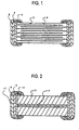
- Fig. 1 shows one exemplary structure of a CR composite electronic part which is fabricated as mentioned above and according to the invention.
- the CR composite electronic part comprises a dielectric layer 2, an internal electrode layer 3, a first metal layer 4, an intermediate oxide layer 5, and a second metal layer 6.
- terminal electrodes constructed of the first metal layer 4, second metal layer 6 and intermediate oxide layer 5 should be each provided on the outside with a plated layer.
- the intermediate oxide layer 5 has a resistance value determined depending on conductivity restricted by the minimum thickness, metal oxides, etc.
- the intermediate oxide layer 5 is formed on both terminals of the CR composite electronic part.
- the intermediate oxide layer may be formed on one terminal alone. In this case, only one of the terminal electrodes contributes to equivalent series resistance. In an ordinary process, however, the intermediate oxide layer is formed on both terminals.
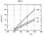
- Fig. 2 shows one exemplary structure of a chip resistor which is fabricated as mentioned above and according to the invention.
- the chip resistor comprises an insulator layer 12, an internal conductor 13, a first metal layer 14, an intermediate oxide layer 15, and a second metal layer 16.
- terminal electrodes constructed of the first metal layer, second metal layer and intermediate oxide layer should be each provided on the outside with a plated layer 17.
- BaCO 3 (having an average particle size of 2.0 ⁇ m) and TiO 2 (having an average particle size of 2.0 ⁇ m) were provided as the main raw material for a dielectric layer.
- the atomic ratio of Ba/Ti was 1.00.
- additives MnCO 3 , MgCO 3 , Y 2 O 3 , and (BaCa)SiO 3 were provided in the respective amounts of 0.2 wt%, 0.2 wt%, 2.1 wt%, and 2.2 wt% relative to BaTiO 3 .
- the obtained calcined powders were mixed with an acrylic resin serving as an organic binder, and methylene chloride and acetone serving as organic solvents to prepare a dielectric slurry.
- the obtained dielectric slurry was formed by a doctor blade process into a dielectric green sheet.
- Powders (having an average particle size of 0.8 ⁇ m) of base metal Ni were provided as an internal electrode material.
- the powders were then milled in a triple roll mill with ethyl cellulose serving as an organic binder and terpineol serving as an organic solvent to prepare a paste for the internal electrode.
- Cu powders (having an average particle size of 0.5 ⁇ m), and Cu powders with 7 wt% of strontium base glass added thereto were provided as a paste material for the first metal layer.
- the powders were milled with an acrylic resin serving as an organic binder and terpineol serving as an organic solvent in a triple roll mill to prepare a paste for each terminal electrode.
- Ag powders (having an average particle size of 0.5 ⁇ m), and Ag powders with 1 wt% of lead borosilicate glass added thereto were provided as a paste material for the second metal layer.
- the powders were milled with an acrylic resin serving as an organic binder and terpineol serving as an organic solvent in a triple roll mill to prepare a paste for each terminal electrode.
- the thus obtained green chip was left in the air at 80°C for 30 minutes for drying. Then, the green chip was fired by holding it at 1,300°C for 3 hours in a moisturized N 2 +H 2 (H 2 : 3%) reducing atmosphere. Further, the green chip was held at 1,000°C for 2 hours in a moisturized H 2 atmosphere having an oxygen partial pressure of 10 -7 atm., thereby obtaining a chip member.
- the paste for the first metal layer obtained by dispersing Cu with glass frit added thereto in an amount of 7 wt% relative to the metal component in an organic vehicle was coated on both ends of the obtained chip member, dried, and held at 770°C for 10 minutes in an N 2 +H 2 atmosphere for firing, thereby forming the first metal layer.
- the paste for the second metal layer obtained by dispersing Ag with glass frit added thereto in an amount of 1 wt% relative to the metal component in an organic vehicle was coated by a dipping process on both ends of the chip member with the first metal layer formed thereof, dried, and held at 600 to 750°C for 10 minutes in the air for firing, thereby forming the second metal layer and, at the same time, oxidizing the surface of the first metal layer to form an intermediate oxide layer.
- firing was carried out at temperatures of 600°C, 650°C, 700°C, and 750°C for holding times of 1 minute, 5 minutes, and 10 minutes for the purpose of controlling the thickness of the second metal layer.
- X-ray diffraction analysis of the second metal layer indicated the presence of Cu 2 O, Cu 3 O 4 , and CuO.
- a nickel plating layer, and a tin-lead alloy plating layer were successively formed by an electrolytic process on each of the obtained samples having such additive compositions as mentioned above to obtain a CR composite electronic part sample which was found to have an electrostatic capacity of 22 ⁇ F.
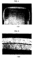
- Each of the obtained samples was also measured for ESR.
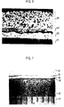
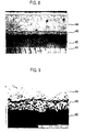
- the results are plotted in Fig. 3. A photograph taken of a section of an end portion of one sample obtained by firing at 650°C for the holding time of 10 minutes is attached hereto as Fig. 4, and an enlarged photograph of Fig. 4 is attached hereto as Fig. 5.
- the intermediate oxide layer (represented by a dark strip region in the vicinity of a middle portion of the terminal electrode) is formed between the first metal layer and the second metal layer.
- the obtained CR composite electronic part was operated as a power supply bypass capacitor for a DC-DC converter at a varying switching frequency between 1 kHz and 10 MHz. As a consequence, it was found that the CR composite electronic part can function normally without causing voltage fluctuations such as oscillation.
- Example 2 A sample was prepared as in Example 1 with the exception that a green chip of 4.5 x 3.2 x 2.0 mm was used. With this sample, it was found that the stability of the circuit can be further enhanced.
- the ESR can be varied or controlled by varying the firing temperature and holding time for firing the second metal layer.
- Ni powders having an average particle size of 0.4 ⁇ m
- Ni-Cu powders having an average particle size of 0.5 ⁇ m
- Fe powders having an average particle size of 0.5 ⁇ m
- Co powders having an average particle size of 0.01 to 10 ⁇ m
- Example 1 Each of the obtained samples was measured for EST as in Example 1. As a result, it was found that substantially similar results are obtained although the ESR measurements are more or less different from those in Example 1.
- Samples were obtained as in Example 1 with the exception that Au powders (having an average particle size of 1.0 ⁇ m), Pt powders (having an average particle size of 0.1 to 5 ⁇ m), Pd powders (having an average particle size of 0.01 to 5 ⁇ m), Rh powders (having an average particle size of 0.1 to 10 ⁇ m), and Ir powders (having an average particle size of 0.1 to 10 ⁇ m) were used as the material for the second metal layer,.
- Au powders having an average particle size of 1.0 ⁇ m
- Pt powders having an average particle size of 0.1 to 5 ⁇ m
- Pd powders having an average particle size of 0.01 to 5 ⁇ m
- Rh powders having an average particle size of 0.1 to 10 ⁇ m
- Ir powders having an average particle size of 0.1 to 10 ⁇ m
- Example 1 Each of the obtained samples was measured for EST as in Example 1. As a result, it was found that substantially similar results are obtained although the ESR measurements are more or less different from those in Example 1.
- Example 1 Ni powders (having an average particle size of 0.5 ⁇ m) that were the metal for the first metal layer, and Ni powders with 7 wt% of strontium base glass added thereto were provided as the paste material for the first metal layer.
- the powders were milled with an acrylic resin serving as an organic binder and terpineol serving as an organic solvent in a triple roll mill to prepare a paste for each terminal electrode.
- Pd powders (having an average particle size of 0.5 ⁇ m) that were the metal for the second metal layer, and Pd powders with 1 wt% of lead borosilicate glass added thereto were provided as the paste material for the second metal layer.
- the powders were milled with an acrylic resin serving as an organic binder and terpineol serving as an organic solvent in a triple roll mill to prepare a paste for each terminal electrode.
- a green chip obtained as in Example 1 was left at 80°C for 30 minutes in the air, and dried. Then, the green chip was held at 1,300°C for 3 hours in a moisturized N 2 +H 2 (H 2 : 3%) reducing atmosphere for firing. Further, the green chip was held at 1,000°C for 2 hours in a moisturized H 2 atmosphere having an oxygen partial pressure of 10 -7 atm. to obtain a chip member.
- the paste for the first metal layer was coated on both ends of the obtained chip member, dried, and fired at 1,000°C for 10 minutes in a neutral or reducing atmosphere to obtain an Ni terminal electrode (a first electrode layer).
- the paste for the second metal layer was coated by a dipping process on the first metal layer, dried, and held at 800°C for 1 minute in the air for firing, thereby completing the second metal layer and, at the same time, oxidizing the surface of the first metal layer to form an intermediate oxide layer.
- the presence of NiO was identified by x-ray diffraction analysis of the intermediate oxide layer.
- a nickel plating layer, and a tin-lead alloy plating layer were successively formed by an electrolytic process on each of the obtained samples having such additive compositions as mentioned above to obtain a CR composite electronic part sample which was found to have an electrostatic capacity of 1 ⁇ F.
- each sample was found to have an ESR of 500 m ⁇ .
- the metal in the paste for the second metal layer was changed from Pd to Pt, too, substantially equivalent results were obtained.
- the obtained CR composite electronic part was operated as a power supply bypass capacitor for a DC-DC converter. As a consequence, it was found that the CR composite electronic part can function normally without causing voltage fluctuations such as oscillation.
- Example 4 A sample was prepared as in Example 4 with the exception that a green chip of 4.5 x 3.2 x 2.0 mm was used. By measurement, the sample was found to have an ESR of 1,000 m ⁇ . This sample was used as a bypass capacitor as mentioned above. It was consequently found that the stability of the circuit is further improved.
- Example 4 the paste for the first metal layer was coated on both ends of the obtained green chip, and dried. At both ends of the green chip with the first metal layer coated thereon, the paste for the second metal layer was coated by a dipping process on the paste for the first metal layer, and dried.
- the green chip with the terminal electrode pastes (for the first, and second metal layers) coated thereon was left at 80°C for 30 minutes in the air for drying. Subsequently, the green chip was held at 1,300°C for 3 hours in a moisturized N 2 +H 2 (H 2 : 3%) reducing atmosphere for firing, then held at 1,000°C for 2 hours in a moisturized H 2 atmosphere having an oxygen partial pressure of 10 -7 atm., and finally held at 700°C for 10 minutes for cooling, thereby forming a chip member and, at the same time, completing the first, and second metal layers simultaneously with the oxidization of the surface of the first metal layer, thereby forming an intermediate oxide layer.
- the presence of NiO was identified by x-ray diffraction analysis of the intermediate oxide layer.
- a nickel plating layer, and a tin-lead alloy plating layer were successively formed by an electrolytic process on each of the obtained samples having such additive compositions as mentioned above to obtain a CR composite electronic part sample which was found to have an electrostatic capacity of 1 ⁇ F.
- each sample was found to have an ESR of 200 m ⁇ .
- the obtained CR composite electronic part was operated as a power supply bypass capacitor for a DC-DC converter.
- the CR composite electronic part can function normally without causing voltage fluctuations such as oscillation.
- a sample was prepared as in Example 5 with the exception that a green chip of 4.5 x 3.2 x 2.0 mm was used. By measurement, the sample was found to have an ESR of 900 m ⁇ . This sample was used as a bypass capacitor as mentioned above. It was consequently found that the stability of the circuit is further improved.
- the foregoing examples are all directed to the application of the invention to a multilayer ceramic capacitor.
- the invention is in no sense limited to such a multilayer ceramic capacitor; the invention may find wide applications in inductors, semiconductors, and other composite electronic parts.
- Cu powders having an average particle size of 0.3 ⁇ m were dispersed with 7 wt% of strontium base glass (having an average particle size of 0.5 ⁇ m) in a vehicle to obtain a paste for the first metal layer.
- Ag powders having an average particle size of 3.0 ⁇ m
- lead base glass having an average particle size of 1.0 ⁇ m
- a commercially available 99.6% alumina substrate was used.
- the paste for the first metal layer was printed on the substrate according to a given pattern by a screen printing process, dried, and fired at 770°C for 10 minutes in an N 2 +H 2 (H 2 : 3%) mixed atmosphere, thereby forming a precursor to the first electrode layer.
- the paste for the first metal layer had a thickness of 20 ⁇ m.
- the paste for the second metal layer was printed on the sintered precursor to the first metal layer in such a way that the precursor to the first metal layer was perfectly covered thereby, dried, and fired at 650°C for 10 minutes in the air.
- an electronic device was obtained, which comprised an intermediate oxide layer including an oxide of Cu contained in the precursor to the first metal layer, the first metal layer, and the second metal layer.
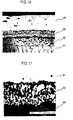
- FIG. 6 A photograph taken of a section of the obtained electronic device is attached hereto as Fig. 6.
- a substrate 21 is provided thereon with a Cu metal layer 22 that is the first metal layer, a Cu oxide layer 23 that is the intermediate oxide layer, and an Ag metal layer 24 that is the second metal layer in the described order.
- EPMA it was identified that oxygen is present in the Cu oxide layer 23, and by x-ray diffraction it was identified that the Cu oxide is Cu 2 O.
- Ni powders having an average particle size of 0.2 ⁇ m
- 7 wt% of strontium base glass having an average particle size of 0.5 ⁇ m
- Ag powders having an average particle size of 3.0 ⁇ m
- lead base glass having an average particle size of 1.0 ⁇ m
- a commercially available 99.6% alumina substrate was used.
- the paste for the first metal layer was printed on the substrate according to a given pattern by a screen printing process, dried, and fired at 900°C for 10 minutes in an N 2 +H 2 (H 2 : 3%) mixed atmosphere, thereby forming a precursor to the first electrode layer.
- the paste for the first metal layer had a thickness of 20 ⁇ m.
- the paste for the second metal layer was printed on the sintered precursor to the first metal layer in such a way that the precursor to the first metal layer was perfectly covered thereby, dried, and fired at 750°C for 10 minutes in the air.
- an electronic device was obtained, which comprised an intermediate oxide layer including an oxide of Ni contained in the precursor to the first metal layer, the first metal layer, and the second metal layer.
- the Ni oxide layer that was an intermediate oxide layer of 3 ⁇ m in thickness could be formed midway between the Ni metal layer that was the first metal layer and the Ag metal layer that was the second metal layer.
- EPMA it was identified that oxygen is present in the Ni oxide layer, and by x-ray diffraction it was identified that the Ni oxide is NiO.
- Mn powders having an average particle size of 1.0 ⁇ m
- strontium base glass having an average particle size of 0.5 ⁇ m
- Pd powders having an average particle size of 0.5 ⁇ m were dispersed with 1 wt% of lead base glass (having an average particle size of 1.0 ⁇ m) in a vehicle to obtain a paste for the second metal layer.
- a commercially available 99.6% alumina substrate was used.
- the paste for the first metal layer was printed on the substrate according to a given pattern by a screen printing process, dried, and fired at 900°C for 10 minutes in an N 2 +H 2 (H 2 : 3%) mixed atmosphere, thereby forming a precursor to the first electrode layer.
- the paste for the first metal layer had a thickness of 20 ⁇ m.
- the paste for the second metal layer was printed on the sintered precursor to the first metal layer in such a way that the precursor to the first metal layer was perfectly covered thereby, dried, and fired at 800°C for 10 minutes in the air.
- an electronic device was obtained, which comprised an intermediate oxide layer including an oxide of Mn contained in the precursor to the first metal layer, the first metal layer, and the second metal layer.
- the Mn oxide layer that was an intermediate oxide layer of 10 ⁇ m in thickness could be formed midway between the Mn metal layer that was the first metal layer and the Pd metal layer that was the second metal layer.
- Cu powders having an average particle size of 0.3 ⁇ m were dispersed with 7 wt% of strontium base glass (having an average particle size of 0.5 ⁇ m) in a vehicle to obtain a paste for the first metal layer.
- Ag powders having an average particle size of 3.0 ⁇ m
- lead base glass having an average particle size of 1.0 ⁇ m
- a commercially available 99.6% alumina substrate was used.
- the paste for the primer metal layer was printed on the substrate according to a given pattern by a screen printing process, dried, and fired at 770°C for 10 minutes in an N 2 +H 2 (H 2 : 3%) mixed atmosphere, thereby forming a primer metal layer.
- the paste for the primer metal layer had a thickness of 20 ⁇ m.
- a 5- ⁇ m thick Ni film that was a plating layer providing the first metal layer was then formed by a known electrolytic plating process on the sintered primer metal layer.
- the paste for the second metal layer was printed on the first metal layer in such a way that the first metal layer was perfectly covered thereby, dried, and fired at 700°C for 10 minutes in the air.
- an electronic device was obtained, which comprised an intermediate oxide layer including an oxide of Ni contained in the first metal layer, the primer metal layer, the first metal layer, and the second metal layer.
- the Ni oxide layer that was a 10- ⁇ m thick intermediate oxide layer could be formed on the Cu metal layer that was the primer metal layer midway between the Ni metal layer that was the first metal layer and the Ag metal layer that was the second metal layer.
- EPMA it was identified that oxygen is present in the Ni oxide layer, and by x-ray diffraction it was identified that the Ni oxide is NiO.
- a resistor chip was prepared to explain an application example of the electronic device according to the invention.
- BaCO 3 (having an average particle size of 2.0 ⁇ m) and TiO 2 (having an average particle size of 2.0 ⁇ m) were provided as the main raw material for an insulator layer.
- the atomic ratio of Ba/Ti was 1.00.
- additives MnCO 3 , MgCO 3 , Y 2 O 3 , and (Baca)SiO 3 were provided in the respective amounts of 0.2 wt%, 0.2 wt%, 2.1 wt%, and 2.2 wt% relative to BaTiO 3 .
- These raw powders were mixed together in an underwater ball mill, and dried.
- the obtained powder mixture was calcined at 1,250°C for 2 hours.
- the calcined product was pulverized in an underwater ball mill, and dried.
- the obtained calcined powders were mixed with an acrylic resin serving as an organic binder, and methylene chloride and acetone serving as organic solvents to prepare an insulator slurry.
- the obtained insulator slurry was formed by a doctor blade process into an insulator green sheet.
- Powders (having an average particle size of 0.8 ⁇ m) of base metal Ni were provided as an internal conductor material.
- the powders were then milled in a triple roll mill with ethyl cellulose serving as an organic binder and terpineol serving as an organic solvent to prepare a paste for the internal conductor.
- Cu powders (having an average particle size of 0.5 ⁇ m), and Cu powders with 7 wt% of strontium base glass added thereto were provided as a paste material for the first metal layer.
- the powders were milled with an acrylic resin serving as an organic binder and terpineol serving as an organic solvent in a triple roll mill to prepare a paste for the first metal layer.
- Ag powders (having an average particle size of 0.5 ⁇ m) were provided as a paste material for the second metal layer.
- the powders were milled with an acrylic resin serving as an organic binder and terpineol serving as an organic solvent in a triple roll mill to prepare a paste for the second metal layer.
- the thus obtained green chip was left in the air at 80°C for 30 minutes for drying. Then, the green chip was fired by holding it at 1,300°C for 3 hours in a moisturized N 2 +H 2 (H 2 : 3%) reducing atmosphere. Further, the green chip was held at 1,000°C for 2 hours in a moisturized H 2 atmosphere having an oxygen partial pressure of 10 -7 atm., thereby obtaining a chip member.
- the paste for the first metal layer was coated on both ends of the obtained chip member, dried, and held at 770°C for 10 minutes in an N 2 +H 2 (H 2 : 4%) atmosphere for firing, thereby forming a precursor (Cu-containing layer) to the first metal layer.
- the Ag-containing paste for the second metal layer was coated by a dipping process on both ends of the chip member on which the precursor to the first metal layer was formed, dried, and held at 620°C for 10 minutes in the air, thereby completing the second metal layer and, at the same time, oxidizing the surface of the precursor to the first metal layer to form an intermediate oxide layer containing copper oxide having a relatively high resistance.
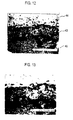
- FIG. 7 A photograph taken of a section of the cut chip resistor is attached hereto as Fig. 7.
- a chip member 31 is successively provided thereon with a first metal layer 32 containing copper, an intermediate oxide layer 33 containing copper oxide, and a second metal layer 34 containing silver, each in a layer form.
- the metal (Ag) 35 in the second metal layer is diffused into the intermediate oxide layer 33.
- the first metal layer had a thickness of about 50 ⁇ m
- the intermediate oxide layer had a thickness of about 10 ⁇ m
- the second metal layer had a thickness of about 20 ⁇ m.
- the presence of oxygen was identified by EPMA analysis of the intermediate oxide layer, and the presence of Cu 2 O, Cu 3 O 4 , and CuO was identified by x-ray diffraction analysis of the intermediate oxide layer.
- the degree of diffusion of Ag in the intermediate oxide layer is represented by the ratio of the average thickness of the intermediate oxide layer 33 with respect to the average thickness of the Ag layer 35 in the intermediate oxide layer. It is understood that the average thickness of each layer was found by SEM section observation. In the following table, the above degree is shown by the ratio of the Ag diffused layer.
- Example 10 A sample was prepared and estimated as in Example 10 with the exception that the average particle size of the Ag powders in the second metal layer was changed to 3.0 ⁇ m. The results are shown in Table 1.
- Example 10 A sample was prepared and estimated as in Example 10 with the exception that the average particle size of the Ag powders in the second metal layer was changed to 5.0 ⁇ m. The results are shown in Table 1.
- Example 10 A sample was prepared and estimated as in Example 10 with the exception that the average particle size of the Ag powders in the second metal layer was changed to 9.0 ⁇ m. The results are shown in Table 1.
- Example 10 A sample was prepared and estimated as in Example 10 with the exception that the average particle size of the Ag powders in the second metal layer was changed to 12.0 ⁇ m. The results are shown in Table 1.
- Example 10 A sample was prepared and estimated as in Example 10 with the exception that 1 wt% of PbO-B 2 O 3 -Ti 2 O 3 base glass frit (having a softening point of 303°C) was added to the paste for the second metal layer. The results are shown in Table 1.
- Example 10 A sample was prepared and estimated as in Example 10 with the exception that 1 wt% of PbO-B 2 O 3 -SiO 2 base glass frit (having a softening point of 470°C) was added to the paste for the second metal layer. The results are shown in Table 1.
- Example 10 A sample was prepared and estimated as in Example 10 with the exception that 1 wt% of ZnO-B 2 O 3 -SiO 2 base glass frit (having a softening point of 610°C) was added to the paste for the second metal layer. The results are shown in Table 1. Sample No. Ag particle size ( ⁇ m) Glass Ratio of Ag in oxidized layer Resistance ( ⁇ ) Tensile strength (kg) Ex. 10 0.5 - 0.95 0.03 3.0 Ex. 11 3 - 0.8 0.1 3.0 Ex. 12 5 - 0.5 0.24 3.1 Ex. 13 9 - 0.1 0.66 3.0 Comp. Ex. 1 12 - 0 0.74 1.1 Ex.
- the inventive samples enable even a relatively low resistance to be easily obtained, and have a sufficient value for tensile strength at terminals. While the correlation between the ratio of the Ag diffused layer and the resistance value may be learned from Table 1 to some extents, it is noted that it is difficult to have a full understanding of the ratio of diffusion of Ag based on the above method. In other words, the values given as the ratio of Ag in the oxidized layer in Table 1 are nothing else than an index to the amount of Ag present in the layer.
- BaCO 3 (having an average particle size of 2.0 ⁇ m) and TiO 2 (having an average particle size of 2.0 ⁇ m) were provided as the main raw material for a dielectric layer.
- the atomic ratio of Ba/Ti was 1.00.
- additives MnCO 3 , MgCO 3 , Y 2 O 3 , and (BaCa)SiO 3 were provided in the respective amounts of 0.2 wt%, 0.2 wt%, 2.1 wt%, and 2.2 wt% relative to BaTiO 3 .
- the obtained calcined powders were mixed with an acrylic resin serving as an organic binder, and methylene chloride and acetone serving as organic solvents to prepare a dielectric slurry.
- the obtained dielectric slurry was formed by a doctor blade process into a dielectric green sheet.
- Powders (having an average particle size of 0.8 ⁇ m) of base metal Ni were provided as an internal conductor material.
- the powders were then milled in a triple roll mill with ethyl cellulose serving as an organic binder and terpineol serving as an organic solvent to prepare a paste for the internal conductor.
- Cu powders (having an average particle size of 0.5 ⁇ m), and Cu powders with 7 wt% of strontium base glass added thereto were provided as a paste material for the first metal layer.
- the powders were milled with an acrylic resin serving as an organic binder and terpineol serving as an organic solvent in a triple roll mill to prepare a paste for the first metal layer.
- Ag powders (having an average particle size of 0.5 ⁇ m) with 1 wt% of lead borosilicate glass added thereto were provided as a paste material for the second metal layer.
- the powders were milled with an acrylic resin serving as an organic binder and terpineol serving as an organic solvent in a triple roll mill to prepare a paste for the second metal layer.
- the thus obtained green chip was left in the air at 80°C for 30 minutes for drying. Then, the green chip was fired by holding it at 1,300°C for 3 hours in a moisturized N 2 +H 2 (H 2 : 3%) reducing atmosphere. Further, the green chip was held at 1,000°C for 2 hours in a moisturized H 2 atmosphere having an oxygen partial pressure of 10 -7 atm., thereby obtaining a chip member.
- the paste for the first metal layer was coated on both ends of the obtained chip member, dried, and held at 770°C for 10 minutes in an N 2 +H 2 (H 2 : 4%) atmosphere for firing, thereby forming a precursor (Cu-containing layer) to the first metal layer.
- the Ag-containing paste for the second metal layer was coated by a dipping process on both ends of the chip member on which the precursor to the first metal layer was formed, dried, heated at a heating rate of 1,800°C/h (sample 1), 2,400°C/h (sample 2), and 3,000°C/h (sample 3), and held at 650°C for 10 minutes in the air, thereby completing the second metal layer and, at the same time, oxidizing the surface of the precursor to the first metal layer to form an intermediate oxide layer containing copper oxide having a relatively high resistance.
- the silver particles contained in the second metal layer were dispersed in the intermediate oxide layer to form a path.
- the effective resistance value depended on the path formed by the Ag particles diffused into the intermediate oxide layer, and became low.
- Figs. 8 to 10 Photographs taken of sections of samples 1 to 3 are attached thereto as Figs. 8 to 10.
- An enlarged photograph of Fig. 10 is attached hereto as Fig. 11
- a photograph taken of an end face of Fig. 9 upon etching of copper oxide thereon by fluoric acid is attached hereto as Fig. 12
- an enlarged photograph of Fig. 12 is attached hereto as Fig. 13.
- a chip member 41 is successively provided thereon with a first metal layer 42 containing copper, an intermediate oxide layer 43 containing copper oxide, and a second metal layer 44 containing silver, each in a layer form. It can also be seen (especially from Fig.
- the metal (Ag) in the second metal layer is dispersed into the intermediate oxide layer 43, and the dispersed metal particles are bound together in a thread form to form a path from the first metal layer 42 to the second metal layer 43.
- the first metal layer had a thickness of about 20 ⁇ m
- the intermediate oxide layer had a thickness of about 12 ⁇ m
- the second metal layer had a thickness of about 30 ⁇ m.
- the presence of oxygen was identified by EPMA analysis of the intermediate oxide layer, and the presence of Cu 2 O, Cu 3 O 4 , and CuO was identified by x-ray diffraction analysis of the intermediate oxide layer.
- Figs. 14 to 16 show resistance value changes with temperature of the inventive sample and comparative sample
- Fig. 15 shows changes-with-temperature in the resistance vs. frequency characteristics of the inventive sample
- Fig. 16 shows changes-with-temperature in the resistance vs. frequency characteristics of the comparative sample.
- the inventive sample is hardly affected by temperature, and so is stable.
- the sample having a large area ratio of Ag particles (rate of dispersion) has low resistance whereas the sample having a small area ratio of Ag particles (rate of dispersion) has high resistance, and both have a substantially proportional relation to each other.
Landscapes
- Engineering & Computer Science (AREA)
- Power Engineering (AREA)
- Microelectronics & Electronic Packaging (AREA)
- Manufacturing & Machinery (AREA)
- Physics & Mathematics (AREA)
- Electromagnetism (AREA)
- Chemical & Material Sciences (AREA)
- Ceramic Engineering (AREA)
- Inorganic Chemistry (AREA)
- Fixed Capacitors And Capacitor Manufacturing Machines (AREA)
- Non-Adjustable Resistors (AREA)
Abstract
Description
| Sample No. | Ag particle size (µm) | Glass | Ratio of Ag in oxidized layer | Resistance (Ω) | Tensile strength (kg) |
| Ex. 10 | 0.5 | - | 0.95 | 0.03 | 3.0 |
| Ex. 11 | 3 | - | 0.8 | 0.1 | 3.0 |
| Ex. 12 | 5 | - | 0.5 | 0.24 | 3.1 |
| Ex. 13 | 9 | - | 0.1 | 0.66 | 3.0 |
| Comp. Ex. 1 | 12 | - | 0 | 0.74 | 1.1 |
| Ex. 14 | 0.5 | PbO-B2O3-Tl2O3 | 0.2 | 0.61 | 3.0 |
| Ex. 15 | 0.5 | PbO-B2O3-SiO2 | 0.97 | 0.02 | 3.1 |
| Ex. 16 | 0.5 | ZnO-B2O3-SiO2 | 0.1 | 0.7 | 2.9 |
| Tensile Strength (kg) | ESR (mΩ) | |
| Sample | 4 | 20 |
| Comparative Sample | 4 | 0.5 |
Claims (38)
- An electronic device comprising a first metal layer containing at least a metal and a second metal layer formed by firing of a metal particle, with an intermediate oxide layer interleaved between said two metal layers, wherein:an oxidation-reduction equilibrium curve for the metal particle contained in said second metal layer is positioned above an oxidation-reduction equilibrium curve for the metal contained in said first metal layer, andsaid intermediate oxide layer comprises an oxide of the metal contained in said first metal layer.
- The electronic device according to claim 1, wherein:electrical conduction is made between said first metal layer and said second metal layer via said intermediate oxide layer, andsaid intermediate oxide layer acts as a resistor.
- The electronic device according to claim 1 or 2, wherein:said first metal layer comprises one or two or more of Fe, Co, Cu, and Ni, andsaid second metal layer comprises one or two or more of Ag, Au, Pt, Pd, Rh, Ir, and Ru.
- The electronic device according to any one of claims 1 to 3, wherein said intermediate oxide layer comprises as an oxide one or two or more of FeO, α-Fe2O3, γ-Fe2O3, Fe3O4, CoO, Co3O4, Cu2O, Cu3O4, CuO, and NiO.
- The electronic device according to any one of claims 1 to 4, wherein said first metal layer, said intermediate oxide layer, and said second metal layer comprise 0 to 20 wt% of glass.
- The electronic device according to any one of claims 1 to 5, wherein:a dielectric layer and an internal electrode are alternately stacked one upon another to form a multilayer structure,terminal electrodes formed at ends of said multilayer structure are electrically connected to said internal electrode to provide a capacitor, andat least one of said terminal electrodes comprises, in order from an internal electrode side, said first metal layer, said intermediate oxide layer, and said second electrode layer.
- The electronic device according to claim 6, wherein an equivalent circuit includes a series CR or (LC)R circuit.
- The electronic device according to claim 6 or 7, wherein a layer of said internal electrode comprises Ni.
- The electronic device according to any one of claim 6 to 8, wherein said terminal electrodes are each provided on an outside with a plated layer.
- An electronic device comprising a first metal layer containing a first metal which provides an oxide upon firing in an oxidizing atmosphere and a second metal layer formed by firing of particles of a second metal which is not oxidized even upon firing in an oxidizing atmosphere, with an intermediate oxide layer interleaved between said two metal layers, wherein:said intermediate oxide layer comprises an oxide of the first metal contained in said first metal layer, while the second metal particles contained in said second metal layer are dispersed in said intermediate oxide layer.
- The electronic device according to claim 10, wherein said second metal particles dispersed in said intermediate oxide layer are present in a metal particle state and/or in a state in which some metal particles are coalesced together.
- The electronic device according to claim 10 or 11, wherein said intermediate oxide layer has a conduction path in which some of said second metal particles dispersed therein are coalesced together.
- The electronic device according to any one of claim 10 to 12, wherein a content of said second metal particles dispersed in said intermediate oxide layer is 20 to 99% provided that a ratio of an area occupied by an oxide of said second metal particles, as identified by observation of a section of the formed intermediate oxide layer, with respect to an entire area of said intermediate oxide layer is represented by an entire area of dispersed particles/the entire area of said intermediate oxide layer x 100.
- The electronic device according to any one of claims 10 to 13, wherein the second metal particles contained in said second metal layer have an average particle size of 0.01 to 10 µm.
- The electronic device according to any one of claims 10 to 14, wherein the first metal particles contained in said first metal layer have an average particle size of 0.1 to 5 µm, and the second metal particles contained in said second metal layer have an average particle size of 0.05 to 5 µm.
- The electronic device according to any one of claims 10 to 15, wherein:the second metal particles contained in said second metal layer comprise one or two or more metal elements selected from Ag, Pt, Rh, Ru, Ir, Au, and Pd, andsaid first metal layer comprises a metal other than said second metal component or an alloy of said metal with said second metal component.
- The electronic device according to any one of claims 10 to 16, wherein said second metal layer comprises a glass frit in an amount of 0 to 20 wt% relative to a total amount of metals.
- The electronic device according to claim 17, wherein said glass frit has a softening point of 350°C to 500°C inclusive.
- The electronic device according to claim 17, wherein said glass frit has a softening point that is equal to or greater than 300°C and lower than 350°C, or greater than 500°C and 1,000°C or lower.
- The electronic device according to any one of claims 10 to 19, wherein said first metal layer comprises one or two or more of Fe, Co, Cu, and Ni.
- The electronic device according to any one of claims 10 to 20, wherein said intermediate oxide layer comprises as an oxide one or two or more of FeO, α-Fe2O3, γ-Fe2O3, Fe3O4, CoO, Co3O4, Cu2O, Cu3O4, CuO, and NiO.
- The electronic device according to any one of claims 10 to 21, wherein:electrical conduction is made between said first metal layer and said second metal layer via said intermediate oxide layer, andsaid intermediate oxide layer acts as a resistor.
- The electronic device according to claim 22, wherein a resistor portion formed from said first metal layer to said second metal layer has a zero or positive temperature coefficient.
- The electronic device according to claim 22 or 23, wherein:a dielectric layer and an internal electrode are alternately stacked one upon another to form a multilayer structure,terminal electrodes formed at ends of said multilayer structure are electrically connected to said internal electrode to provide a capacitor, andat least one of said terminal electrodes comprises, in order from an internal electrode side, said first metal layer, said intermediate oxide layer, and said second electrode layer.
- The electronic device according to any one of claims 22 to 24, wherein an equivalent circuit includes a series CR or (LC)R circuit.
- The electronic device according to claim 24 or 25, wherein a layer of said internal electrode comprises Ni.
- The electronic device according to any one of claims 24 to 26, wherein said terminal electrodes are each provided on an outside with a plated layer.
- A method of fabricating an electronic device comprising steps of:providing pastes for first and second metal layers in which at least metal particles are dispersed in a vehicle, provided that an oxidation-reduction equilibrium curve for a metal contained in said paste for the second metal layer is positioned above an oxidation-reduction equilibrium curve for a metal contained in said paste for the first metal layer,coating, and drying said paste for the first metal layer on a substrate,carrying out firing in a neutral or reducing atmosphere in which the metal contained in said paste for the first metal layer is not oxidized, thereby obtaining a precursor to the first metal layer,coating, and drying said paste for the second metal layer on said precursor to the first metal layer, andcarrying out firing under a partial oxygen pressure condition in which the metal contained in said precursor to the first metal layer is oxidized but the metal contained in said paste for the second metal layer is not oxidized, thereby forming an intermediate oxide layer on an interface of said precursor to the first metal layer with respect to said paste for the second metal layer and obtaining the first metal layer and the second metal layer.
- The electronic device fabrication method according to claim 28, which comprises steps of:coating, drying, and firing said paste for the first metal layer to form a primer metal layer,forming a metal thin film on said primer layer by a plating process to form the first metal layer, andcoating said paste for the second metal layer on the first metal layer.
- A method of fabricating an electronic device, comprising steps of:providing a paste for a first metal layer in which first metal particles converted to an oxide upon firing in an oxidizing atmosphere are dispersed in at least a vehicle, and a paste for a second metal layer in which second metal particles not oxidized even upon firing in an oxidizing atmosphere are dispersed in at least a vehicle,coating, and drying said paste for the first metal layer on a substrate,carrying out firing in a neutral or reducing atmosphere in which the metal contained in said paste for the first metal layer is not oxidized, thereby forming a precursor to the first metal layer,coating, and drying said paste for the second metal layer on said precursor to the first metal layer, andcarrying out firing in an oxidizing atmosphere to oxidize an interface of said precursor to the first metal layer with respect to said paste for the second metal layer, whereby an intermediate oxide layer is formed thereon and the second metal particles contained in the second metal layer are dispersed in said intermediate oxide layer, so that the first metal layer, the intermediate oxide layer, and the second metal layer are obtained.
- The electronic device fabrication method according to claim 30, which comprises steps of:coating, drying, and firing said paste for the first metal layer to form a primer metal layer,forming a metal thin film on said primer metal layer by a plating process to form the first metal layer, andcoating said paste for the second metal layer on the first metal layer.
- The electronic device fabrication method according to claim 30 or 31, wherein an average particle size of the second metal particles contained in said paste for the second metal layer is varied between 0.01 µm and 20 µm to regulate a resistance value of said intermediate oxide layer.
- The electronic device fabrication method according to any one of claims 30 to 32, wherein said paste for the second metal layer comprises a glass frit in an amount of 0 to 20 wt% relative to a total amount of metals, anda softening point of said glass frit is regulated to regulate the resistance value of said intermediate oxide layer.
- The electronic device fabrication method according to any one of claims 30 to 33, wherein the first metal particles contained in the first metal layer have an average particle size of 0.1 to 5 µm, the second metal particles in the second metal layer have an average particle size of 0.05 to 5 µm, and the second metal particles contained in the second metal layer are dispersed from the second metal layer to the first metal layer to form a path of the second metal particles.
- The electronic device fabrication method according to any one of claims 30 to 34, wherein:a dielectric layer and an internal electrode layer are alternately stacked one upon another to form a green chip,said green chip is fired into a chip member,said paste for the first metal layer is coated on said chip member and firing is carried out in a neutral or reducing atmosphere to form a precursor to the first metal layer, and the intermediate oxide layer,said paste for the second metal layer is coated on said precursor, andfiring is carried out in an oxidizing atmosphere to oxidize the vicinity of an interface of said precursor to the first metal layer and intermediate oxide layer with respect to the second metal layer, thereby forming terminal electrodes.
- The electronic device fabrication method according to any one of claims 30 to 34, wherein:a dielectric layer and an internal electrode layer are alternately stacked on upon another to form a green chip,said green chip is fired into a chip member,said paste for the first metal layer is coated on said chip member,said paste for the second metal layer is coated on said paste for the first metal layer,firing is carried out in a neutral or reducing atmosphere to obtain a fired assemblysaid fired assembly is placed in an oxidizing atmosphere in the process of cooling to oxidize the vicinity of an interface of the fired paste for the first metal layer with respect to the second metal layer, thereby forming a terminal electrode layer.
- The electronic device fabrication method according to any one of claims 30 to 34, wherein:a dielectric layer and an internal electrode layer are alternately stacked one upon another to form a green chip,a paste for a first electrode layer is coated on said green chip,said paste for the second metal layer is coated on said paste for the first electrode layer,firing is carried out in a reducing atmosphere to obtain a fired assembly, andsaid fired assembly is placed in an oxidizing atmosphere in the process of cooling to oxidize the vicinity of an interface of the fired paste for the first metal layer with respect to the second metal layer, thereby forming terminal electrodes.
- The electronic device fabrication method according to any one of claims 35 to 37, wherein the first metal layer comprises Cu and/or Ni, and the second metal layer comprises one or two or more of Ag, Pd, Pt, Rh, Ir, and Ru.
Applications Claiming Priority (9)
| Application Number | Priority Date | Filing Date | Title |
|---|---|---|---|
| JP28911097A JP3831497B2 (en) | 1997-10-06 | 1997-10-06 | CR composite electronic component and manufacturing method thereof |
| JP28911097 | 1997-10-06 | ||
| JP31146097 | 1997-10-27 | ||
| JP31146097 | 1997-10-27 | ||
| JP36177597 | 1997-12-10 | ||
| JP36177597 | 1997-12-10 | ||
| JP10216898 | 1998-03-30 | ||
| JP10216898 | 1998-03-30 | ||
| PCT/JP1998/004521 WO1999018588A1 (en) | 1997-10-06 | 1998-10-06 | Electronic device and method of producing the same |
Publications (3)
| Publication Number | Publication Date |
|---|---|
| EP0964415A1 true EP0964415A1 (en) | 1999-12-15 |
| EP0964415A4 EP0964415A4 (en) | 2005-12-28 |
| EP0964415B1 EP0964415B1 (en) | 2009-07-15 |
Family
ID=27468986
Family Applications (1)
| Application Number | Title | Priority Date | Filing Date |
|---|---|---|---|
| EP98945643A Expired - Lifetime EP0964415B1 (en) | 1997-10-06 | 1998-10-06 | Electronic device and method of producing the same |
Country Status (7)
| Country | Link |
|---|---|
| US (1) | US6124769A (en) |
| EP (1) | EP0964415B1 (en) |
| KR (1) | KR100345031B1 (en) |
| CN (1) | CN100380541C (en) |
| DE (1) | DE69840976D1 (en) |
| TW (1) | TW414898B (en) |
| WO (1) | WO1999018588A1 (en) |
Cited By (47)
| Publication number | Priority date | Publication date | Assignee | Title |
|---|---|---|---|---|
| EP1156498A3 (en) * | 2000-04-25 | 2006-06-07 | TDK Corporation | Multi-layer ceramic electronic device and method for producing same |
| US7605498B2 (en) | 2007-10-15 | 2009-10-20 | Ampt, Llc | Systems for highly efficient solar power conversion |
| US7919953B2 (en) | 2007-10-23 | 2011-04-05 | Ampt, Llc | Solar power capacitor alternative switch circuitry system for enhanced capacitor life |
| GB2520676A (en) * | 2013-09-27 | 2015-06-03 | Continental Automotive Systems | Sensor package with wire bondable chip capacitors |
| US9397497B2 (en) | 2013-03-15 | 2016-07-19 | Ampt, Llc | High efficiency interleaved solar power supply system |
| US9442504B2 (en) | 2009-04-17 | 2016-09-13 | Ampt, Llc | Methods and apparatus for adaptive operation of solar power systems |
| US9466737B2 (en) | 2009-10-19 | 2016-10-11 | Ampt, Llc | Solar panel string converter topology |
| US10007288B2 (en) | 2012-03-05 | 2018-06-26 | Solaredge Technologies Ltd. | Direct current link circuit |
| US10097007B2 (en) | 2006-12-06 | 2018-10-09 | Solaredge Technologies Ltd. | Method for distributed power harvesting using DC power sources |
| US10230245B2 (en) | 2006-12-06 | 2019-03-12 | Solaredge Technologies Ltd | Battery power delivery module |
| US10230310B2 (en) | 2016-04-05 | 2019-03-12 | Solaredge Technologies Ltd | Safety switch for photovoltaic systems |
| US10381977B2 (en) | 2012-01-30 | 2019-08-13 | Solaredge Technologies Ltd | Photovoltaic panel circuitry |
| US10396662B2 (en) | 2011-09-12 | 2019-08-27 | Solaredge Technologies Ltd | Direct current link circuit |
| US10447150B2 (en) | 2006-12-06 | 2019-10-15 | Solaredge Technologies Ltd. | Distributed power harvesting systems using DC power sources |
| US10461687B2 (en) | 2008-12-04 | 2019-10-29 | Solaredge Technologies Ltd. | Testing of a photovoltaic panel |
| US10468878B2 (en) | 2008-05-05 | 2019-11-05 | Solaredge Technologies Ltd. | Direct current power combiner |
| US10516336B2 (en) | 2007-08-06 | 2019-12-24 | Solaredge Technologies Ltd. | Digital average input current control in power converter |
| US10608553B2 (en) | 2012-01-30 | 2020-03-31 | Solaredge Technologies Ltd. | Maximizing power in a photovoltaic distributed power system |
| US10637393B2 (en) | 2006-12-06 | 2020-04-28 | Solaredge Technologies Ltd. | Distributed power harvesting systems using DC power sources |
| US10644589B2 (en) | 2007-12-05 | 2020-05-05 | Solaredge Technologies Ltd. | Parallel connected inverters |
| US10666125B2 (en) | 2011-01-12 | 2020-05-26 | Solaredge Technologies Ltd. | Serially connected inverters |
| US10673222B2 (en) | 2010-11-09 | 2020-06-02 | Solaredge Technologies Ltd. | Arc detection and prevention in a power generation system |
| US10673229B2 (en) | 2010-11-09 | 2020-06-02 | Solaredge Technologies Ltd. | Arc detection and prevention in a power generation system |
| US10778025B2 (en) | 2013-03-14 | 2020-09-15 | Solaredge Technologies Ltd. | Method and apparatus for storing and depleting energy |
| US10931119B2 (en) | 2012-01-11 | 2021-02-23 | Solaredge Technologies Ltd. | Photovoltaic module |
| US10931228B2 (en) | 2010-11-09 | 2021-02-23 | Solaredge Technologies Ftd. | Arc detection and prevention in a power generation system |
| US10969412B2 (en) | 2009-05-26 | 2021-04-06 | Solaredge Technologies Ltd. | Theft detection and prevention in a power generation system |
| US10992238B2 (en) | 2012-01-30 | 2021-04-27 | Solaredge Technologies Ltd. | Maximizing power in a photovoltaic distributed power system |
| US11018623B2 (en) | 2016-04-05 | 2021-05-25 | Solaredge Technologies Ltd. | Safety switch for photovoltaic systems |
| US11031861B2 (en) | 2006-12-06 | 2021-06-08 | Solaredge Technologies Ltd. | System and method for protection during inverter shutdown in distributed power installations |
| US11177663B2 (en) | 2016-04-05 | 2021-11-16 | Solaredge Technologies Ltd. | Chain of power devices |
| US20220013295A1 (en) * | 2020-07-07 | 2022-01-13 | Murata Manufacturing Co., Ltd. | Electronic component |
| US11264947B2 (en) | 2007-12-05 | 2022-03-01 | Solaredge Technologies Ltd. | Testing of a photovoltaic panel |
| US11309832B2 (en) | 2006-12-06 | 2022-04-19 | Solaredge Technologies Ltd. | Distributed power harvesting systems using DC power sources |
| US11569659B2 (en) | 2006-12-06 | 2023-01-31 | Solaredge Technologies Ltd. | Distributed power harvesting systems using DC power sources |
| US11569660B2 (en) | 2006-12-06 | 2023-01-31 | Solaredge Technologies Ltd. | Distributed power harvesting systems using DC power sources |
| US11579235B2 (en) | 2006-12-06 | 2023-02-14 | Solaredge Technologies Ltd. | Safety mechanisms, wake up and shutdown methods in distributed power installations |
| US11598652B2 (en) | 2006-12-06 | 2023-03-07 | Solaredge Technologies Ltd. | Monitoring of distributed power harvesting systems using DC power sources |
| US11687112B2 (en) | 2006-12-06 | 2023-06-27 | Solaredge Technologies Ltd. | Distributed power harvesting systems using DC power sources |
| US11728768B2 (en) | 2006-12-06 | 2023-08-15 | Solaredge Technologies Ltd. | Pairing of components in a direct current distributed power generation system |
| US11735910B2 (en) | 2006-12-06 | 2023-08-22 | Solaredge Technologies Ltd. | Distributed power system using direct current power sources |
| US11855231B2 (en) | 2006-12-06 | 2023-12-26 | Solaredge Technologies Ltd. | Distributed power harvesting systems using DC power sources |
| US11881814B2 (en) | 2005-12-05 | 2024-01-23 | Solaredge Technologies Ltd. | Testing of a photovoltaic panel |
| US11888387B2 (en) | 2006-12-06 | 2024-01-30 | Solaredge Technologies Ltd. | Safety mechanisms, wake up and shutdown methods in distributed power installations |
| US12027849B2 (en) | 2006-12-06 | 2024-07-02 | Solaredge Technologies Ltd. | Distributed power system using direct current power sources |
| US12057807B2 (en) | 2016-04-05 | 2024-08-06 | Solaredge Technologies Ltd. | Chain of power devices |
| US12418177B2 (en) | 2009-10-24 | 2025-09-16 | Solaredge Technologies Ltd. | Distributed power system using direct current power sources |
Families Citing this family (41)
| Publication number | Priority date | Publication date | Assignee | Title |
|---|---|---|---|---|
| DE19935677B4 (en) * | 1999-07-29 | 2005-07-07 | Robert Bosch Gmbh | Paste for the screen printing of electrical structures on carrier substrates |
| JP2001185437A (en) * | 1999-12-24 | 2001-07-06 | Taiyo Yuden Co Ltd | Laminated ceramic capacitor |
| US6193134B1 (en) * | 2000-06-26 | 2001-02-27 | Advanced Micro Devices, Inc. | Determination of quality of bonding between a conductive ball and a conductive pad within an IC package |
| US6461931B1 (en) * | 2000-08-29 | 2002-10-08 | Micron Technology, Inc. | Thin dielectric films for DRAM storage capacitors |
| US7378719B2 (en) * | 2000-12-20 | 2008-05-27 | Micron Technology, Inc. | Low leakage MIM capacitor |
| US7038572B2 (en) * | 2001-03-19 | 2006-05-02 | Vishay Dale Electronics, Inc. | Power chip resistor |
| JP3882718B2 (en) * | 2002-08-29 | 2007-02-21 | 株式会社村田製作所 | Manufacturing method of thin film laminated electronic component |
| JP4047760B2 (en) * | 2003-04-28 | 2008-02-13 | ローム株式会社 | Chip resistor and manufacturing method thereof |
| US6972473B2 (en) * | 2003-08-12 | 2005-12-06 | Tessera, Inc. | Structure and method of making an enhanced surface area capacitor |
| DE102004036431B4 (en) | 2004-07-27 | 2019-01-03 | Robert Bosch Gmbh | Electric ceramic capacitor |
| US20060034029A1 (en) * | 2004-08-13 | 2006-02-16 | Cyntec Company | Current detector with improved resistance adjustable range and heat dissipation |
| WO2006022060A1 (en) * | 2004-08-27 | 2006-03-02 | Murata Manufacturing Co., Ltd. | Multilayer ceramic capacitor and method for adjusting equivalent series resistance thereof |
| JP3861927B1 (en) * | 2005-07-07 | 2006-12-27 | 株式会社村田製作所 | Electronic component, electronic component mounting structure, and electronic component manufacturing method |
| KR100649092B1 (en) * | 2005-11-02 | 2006-11-27 | 한국과학기술연구원 | Metal oxide-based supercapacitor composed of metal oxide coated titanium oxide ultrafine fiber and method for manufacturing same |
| TWI430293B (en) * | 2006-08-10 | 2014-03-11 | Kamaya Electric Co Ltd | Production method of corner plate type chip resistor and corner plate type chip resistor |
| WO2008099772A1 (en) * | 2007-02-14 | 2008-08-21 | Murata Manufacturing Co., Ltd. | Laminated ceramic capacitor and method for manufacturing the same |
| JP4861946B2 (en) * | 2007-09-26 | 2012-01-25 | 株式会社ノリタケカンパニーリミテド | Manufacturing method of film conductor by high-speed firing |
| WO2010042124A1 (en) * | 2008-10-10 | 2010-04-15 | Ampt, Llc | Novel solar power circuits and powering methods |
| CN101618962B (en) * | 2009-07-28 | 2012-05-23 | 四川西汉电子科技有限责任公司 | Low-temperature-coefficient high-resistivity thermosensitive material and preparation method thereof |
| TWI523050B (en) * | 2011-11-18 | 2016-02-21 | Prosperity Dielectrics Co Ltd | Multi - layer co - fired laminated stacked chip resistors and manufacturing method thereof |
| KR101558025B1 (en) * | 2011-11-30 | 2015-10-07 | 삼성전기주식회사 | Laminated ceramic electronic parts and fabrication method thereof |
| WO2013140903A1 (en) * | 2012-03-19 | 2013-09-26 | 株式会社村田製作所 | Ceramic electronic component |
| KR20130111000A (en) * | 2012-03-30 | 2013-10-10 | 삼성전기주식회사 | Laminated ceramic electronic parts and fabricating method thereof |
| AT512041B1 (en) * | 2012-05-04 | 2013-05-15 | Mikroelektronik Ges Mit Beschraenkter Haftung Ab | Method for producing a metallized substrate |
| JP5910533B2 (en) | 2012-05-08 | 2016-04-27 | 株式会社村田製作所 | Electronic component, electronic component-embedded substrate, and electronic component manufacturing method |
| KR20140014773A (en) * | 2012-07-26 | 2014-02-06 | 삼성전기주식회사 | Multi-layered ceramic electronic parts and method of manufacturing the same |
| KR101688299B1 (en) * | 2012-08-10 | 2016-12-20 | 가부시키가이샤 무라타 세이사쿠쇼 | Magnetic material composition and coil component |
| JP2015026838A (en) * | 2013-10-22 | 2015-02-05 | 株式会社村田製作所 | Capacitor |
| KR101808794B1 (en) * | 2015-05-07 | 2018-01-18 | 주식회사 모다이노칩 | Laminated device |
| CN104851590A (en) * | 2015-05-19 | 2015-08-19 | 北京元六鸿远电子技术有限公司 | Capacitor with multiple types of capacitance |
| JP6724321B2 (en) * | 2015-09-15 | 2020-07-15 | Tdk株式会社 | Laminated electronic components |
| JP6547569B2 (en) * | 2015-10-08 | 2019-07-24 | Tdk株式会社 | Electronic parts |
| KR102059441B1 (en) | 2017-01-02 | 2019-12-27 | 삼성전기주식회사 | Capacitor Component |
| JP7089402B2 (en) * | 2018-05-18 | 2022-06-22 | 太陽誘電株式会社 | Multilayer ceramic capacitors and their manufacturing methods |
| CN109346322A (en) * | 2018-10-17 | 2019-02-15 | 成都宏明电子科大新材料有限公司 | A kind of pulse power ceramic capacitor, termination electrode and preparation method |
| CN109841405B (en) * | 2019-04-18 | 2021-02-19 | 北京元六鸿远电子科技股份有限公司 | Silver-terminated electrode slurry for low-temperature sintered MLCC |
| US11222878B2 (en) | 2019-04-30 | 2022-01-11 | Ab Mikroelektronik Gesellschaft Mit Beschraenkter Haftung | Electronic power module |
| KR102333094B1 (en) | 2019-07-08 | 2021-12-01 | 삼성전기주식회사 | Capacitor component |
| JP7188356B2 (en) * | 2019-10-25 | 2022-12-13 | 株式会社村田製作所 | Ceramic electronic component and method for manufacturing ceramic electronic component |
| CN111137954B (en) * | 2019-11-22 | 2021-08-03 | 清华大学 | Photocathode, method for preparing the same, and method for removing chloroacetic acid contained in water |
| JP7535005B2 (en) * | 2021-03-31 | 2024-08-15 | Tdk株式会社 | Multilayer Electronic Components |
Family Cites Families (8)
| Publication number | Priority date | Publication date | Assignee | Title |
|---|---|---|---|---|
| US3353124A (en) * | 1963-04-18 | 1967-11-14 | Globe Union Inc | Nickel oxide capacitors |
| JPH01316923A (en) * | 1988-06-16 | 1989-12-21 | Matsushita Electric Ind Co Ltd | Electrode for ceramic electronic components and its manufacturing method |
| JPH04154104A (en) * | 1990-10-18 | 1992-05-27 | Hitachi Aic Inc | Laminated ceramic capacitor |
| JP2943380B2 (en) * | 1991-04-17 | 1999-08-30 | 松下電器産業株式会社 | Multilayer ceramic capacitor and manufacturing method thereof |
| JP2578264B2 (en) * | 1991-05-15 | 1997-02-05 | 太陽誘電株式会社 | Adjustment method of equivalent series resistance of ceramic capacitor |
| JPH0513266A (en) * | 1991-06-28 | 1993-01-22 | Murata Mfg Co Ltd | External electrode structure of laminated electronic component |
| JPH05283283A (en) * | 1992-03-31 | 1993-10-29 | Mitsubishi Materials Corp | Chip type CR composite element and manufacturing method thereof |
| JPH10312934A (en) * | 1997-05-13 | 1998-11-24 | Tdk Corp | Cr composite electronic component and its manufacture |
-
1998
- 1998-10-06 DE DE69840976T patent/DE69840976D1/en not_active Expired - Lifetime
- 1998-10-06 TW TW087116661A patent/TW414898B/en not_active IP Right Cessation
- 1998-10-06 KR KR1019997004881A patent/KR100345031B1/en not_active Expired - Fee Related
- 1998-10-06 WO PCT/JP1998/004521 patent/WO1999018588A1/en not_active Ceased
- 1998-10-06 EP EP98945643A patent/EP0964415B1/en not_active Expired - Lifetime
- 1998-10-06 CN CNB988014807A patent/CN100380541C/en not_active Expired - Fee Related
-
1999
- 1999-06-07 US US09/327,169 patent/US6124769A/en not_active Expired - Lifetime
Cited By (132)
| Publication number | Priority date | Publication date | Assignee | Title |
|---|---|---|---|---|
| EP1156498A3 (en) * | 2000-04-25 | 2006-06-07 | TDK Corporation | Multi-layer ceramic electronic device and method for producing same |
| US11881814B2 (en) | 2005-12-05 | 2024-01-23 | Solaredge Technologies Ltd. | Testing of a photovoltaic panel |
| US11687112B2 (en) | 2006-12-06 | 2023-06-27 | Solaredge Technologies Ltd. | Distributed power harvesting systems using DC power sources |
| US11658482B2 (en) | 2006-12-06 | 2023-05-23 | Solaredge Technologies Ltd. | Distributed power harvesting systems using DC power sources |
| US12276997B2 (en) | 2006-12-06 | 2025-04-15 | Solaredge Technologies Ltd. | Distributed power harvesting systems using DC power sources |
| US12224706B2 (en) | 2006-12-06 | 2025-02-11 | Solaredge Technologies Ltd. | Pairing of components in a direct current distributed power generation system |
| US11043820B2 (en) | 2006-12-06 | 2021-06-22 | Solaredge Technologies Ltd. | Battery power delivery module |
| US12107417B2 (en) | 2006-12-06 | 2024-10-01 | Solaredge Technologies Ltd. | Distributed power harvesting systems using DC power sources |
| US12068599B2 (en) | 2006-12-06 | 2024-08-20 | Solaredge Technologies Ltd. | System and method for protection during inverter shutdown in distributed power installations |
| US12046940B2 (en) | 2006-12-06 | 2024-07-23 | Solaredge Technologies Ltd. | Battery power control |
| US12032080B2 (en) | 2006-12-06 | 2024-07-09 | Solaredge Technologies Ltd. | Safety mechanisms, wake up and shutdown methods in distributed power installations |
| US12027970B2 (en) | 2006-12-06 | 2024-07-02 | Solaredge Technologies Ltd. | Safety mechanisms, wake up and shutdown methods in distributed power installations |
| US12027849B2 (en) | 2006-12-06 | 2024-07-02 | Solaredge Technologies Ltd. | Distributed power system using direct current power sources |
| US11962243B2 (en) | 2006-12-06 | 2024-04-16 | Solaredge Technologies Ltd. | Method for distributed power harvesting using DC power sources |
| US11961922B2 (en) | 2006-12-06 | 2024-04-16 | Solaredge Technologies Ltd. | Distributed power harvesting systems using DC power sources |
| US11888387B2 (en) | 2006-12-06 | 2024-01-30 | Solaredge Technologies Ltd. | Safety mechanisms, wake up and shutdown methods in distributed power installations |
| US12316274B2 (en) | 2006-12-06 | 2025-05-27 | Solaredge Technologies Ltd. | Pairing of components in a direct current distributed power generation system |
| US11855231B2 (en) | 2006-12-06 | 2023-12-26 | Solaredge Technologies Ltd. | Distributed power harvesting systems using DC power sources |
| US11735910B2 (en) | 2006-12-06 | 2023-08-22 | Solaredge Technologies Ltd. | Distributed power system using direct current power sources |
| US11682918B2 (en) | 2006-12-06 | 2023-06-20 | Solaredge Technologies Ltd. | Battery power delivery module |
| US11728768B2 (en) | 2006-12-06 | 2023-08-15 | Solaredge Technologies Ltd. | Pairing of components in a direct current distributed power generation system |
| US10230245B2 (en) | 2006-12-06 | 2019-03-12 | Solaredge Technologies Ltd | Battery power delivery module |
| US12281919B2 (en) | 2006-12-06 | 2025-04-22 | Solaredge Technologies Ltd. | Monitoring of distributed power harvesting systems using DC power sources |
| US11031861B2 (en) | 2006-12-06 | 2021-06-08 | Solaredge Technologies Ltd. | System and method for protection during inverter shutdown in distributed power installations |
| US10097007B2 (en) | 2006-12-06 | 2018-10-09 | Solaredge Technologies Ltd. | Method for distributed power harvesting using DC power sources |
| US11598652B2 (en) | 2006-12-06 | 2023-03-07 | Solaredge Technologies Ltd. | Monitoring of distributed power harvesting systems using DC power sources |
| US11063440B2 (en) | 2006-12-06 | 2021-07-13 | Solaredge Technologies Ltd. | Method for distributed power harvesting using DC power sources |
| US10447150B2 (en) | 2006-12-06 | 2019-10-15 | Solaredge Technologies Ltd. | Distributed power harvesting systems using DC power sources |
| US11594882B2 (en) | 2006-12-06 | 2023-02-28 | Solaredge Technologies Ltd. | Distributed power harvesting systems using DC power sources |
| US11594881B2 (en) | 2006-12-06 | 2023-02-28 | Solaredge Technologies Ltd. | Distributed power harvesting systems using DC power sources |
| US11183922B2 (en) | 2006-12-06 | 2021-11-23 | Solaredge Technologies Ltd. | Distributed power harvesting systems using DC power sources |
| US11594880B2 (en) | 2006-12-06 | 2023-02-28 | Solaredge Technologies Ltd. | Distributed power harvesting systems using DC power sources |
| US12388492B2 (en) | 2006-12-06 | 2025-08-12 | Solaredge Technologies Ltd. | Safety mechanisms, wake up and shutdown methods in distributed power installations |
| US10637393B2 (en) | 2006-12-06 | 2020-04-28 | Solaredge Technologies Ltd. | Distributed power harvesting systems using DC power sources |
| US11579235B2 (en) | 2006-12-06 | 2023-02-14 | Solaredge Technologies Ltd. | Safety mechanisms, wake up and shutdown methods in distributed power installations |
| US11575261B2 (en) | 2006-12-06 | 2023-02-07 | Solaredge Technologies Ltd. | Distributed power harvesting systems using DC power sources |
| US10673253B2 (en) | 2006-12-06 | 2020-06-02 | Solaredge Technologies Ltd. | Battery power delivery module |
| US11575260B2 (en) | 2006-12-06 | 2023-02-07 | Solaredge Technologies Ltd. | Distributed power harvesting systems using DC power sources |
| US11569660B2 (en) | 2006-12-06 | 2023-01-31 | Solaredge Technologies Ltd. | Distributed power harvesting systems using DC power sources |
| US11569659B2 (en) | 2006-12-06 | 2023-01-31 | Solaredge Technologies Ltd. | Distributed power harvesting systems using DC power sources |
| US11476799B2 (en) | 2006-12-06 | 2022-10-18 | Solaredge Technologies Ltd. | Distributed power harvesting systems using DC power sources |
| US11309832B2 (en) | 2006-12-06 | 2022-04-19 | Solaredge Technologies Ltd. | Distributed power harvesting systems using DC power sources |
| US8093756B2 (en) | 2007-02-15 | 2012-01-10 | Ampt, Llc | AC power systems for renewable electrical energy |
| US10516336B2 (en) | 2007-08-06 | 2019-12-24 | Solaredge Technologies Ltd. | Digital average input current control in power converter |
| US11594968B2 (en) | 2007-08-06 | 2023-02-28 | Solaredge Technologies Ltd. | Digital average input current control in power converter |
| US10608437B2 (en) | 2007-10-15 | 2020-03-31 | Ampt, Llc | Feedback based photovoltaic conversion systems |
| US9438037B2 (en) | 2007-10-15 | 2016-09-06 | Ampt, Llc | Systems for optimized solar power inversion |
| US9673630B2 (en) | 2007-10-15 | 2017-06-06 | Ampt, Llc | Protected conversion solar power system |
| US7605498B2 (en) | 2007-10-15 | 2009-10-20 | Ampt, Llc | Systems for highly efficient solar power conversion |
| US10326283B2 (en) | 2007-10-15 | 2019-06-18 | Ampt, Llc | Converter intuitive photovoltaic electrical energy power system |
| US7719140B2 (en) | 2007-10-15 | 2010-05-18 | Ampt, Llc | Systems for boundary controlled solar power conversion |
| US12003110B2 (en) | 2007-10-15 | 2024-06-04 | Ampt, Llc | Optimized conversion system |
| US11070062B2 (en) | 2007-10-15 | 2021-07-20 | Ampt, Llc | Photovoltaic conversion systems |
| US7843085B2 (en) | 2007-10-15 | 2010-11-30 | Ampt, Llc | Systems for highly efficient solar power |
| US11070063B2 (en) | 2007-10-15 | 2021-07-20 | Ampt, Llc | Method for alternating conversion solar power |
| US12027867B2 (en) | 2007-10-15 | 2024-07-02 | Ampt, Llc | Coordinated converter reactively altering disabling photovoltaic electrical energy power system |
| US8004116B2 (en) | 2007-10-15 | 2011-08-23 | Ampt, Llc | Highly efficient solar power systems |
| US10886746B1 (en) | 2007-10-15 | 2021-01-05 | Ampt, Llc | Alternating conversion solar power system |
| US12027869B2 (en) | 2007-10-15 | 2024-07-02 | Ampt, Llc | Optimized photovoltaic conversion configuration |
| US8482153B2 (en) | 2007-10-15 | 2013-07-09 | Ampt, Llc | Systems for optimized solar power inversion |
| US11289917B1 (en) | 2007-10-15 | 2022-03-29 | Ampt, Llc | Optimized photovoltaic conversion system |
| US8242634B2 (en) | 2007-10-15 | 2012-08-14 | Ampt, Llc | High efficiency remotely controllable solar energy system |
| US8304932B2 (en) | 2007-10-15 | 2012-11-06 | Ampt, Llc | Efficient solar energy power creation systems |
| US11228182B2 (en) | 2007-10-15 | 2022-01-18 | Ampt, Llc | Converter disabling photovoltaic electrical energy power system |
| US8461811B2 (en) | 2007-10-23 | 2013-06-11 | Ampt, Llc | Power capacitor alternative switch circuitry system for enhanced capacitor life |
| US7919953B2 (en) | 2007-10-23 | 2011-04-05 | Ampt, Llc | Solar power capacitor alternative switch circuitry system for enhanced capacitor life |
| US11183923B2 (en) | 2007-12-05 | 2021-11-23 | Solaredge Technologies Ltd. | Parallel connected inverters |
| US11264947B2 (en) | 2007-12-05 | 2022-03-01 | Solaredge Technologies Ltd. | Testing of a photovoltaic panel |
| US11183969B2 (en) | 2007-12-05 | 2021-11-23 | Solaredge Technologies Ltd. | Testing of a photovoltaic panel |
| US11693080B2 (en) | 2007-12-05 | 2023-07-04 | Solaredge Technologies Ltd. | Parallel connected inverters |
| US11894806B2 (en) | 2007-12-05 | 2024-02-06 | Solaredge Technologies Ltd. | Testing of a photovoltaic panel |
| US12055647B2 (en) | 2007-12-05 | 2024-08-06 | Solaredge Technologies Ltd. | Parallel connected inverters |
| US10644589B2 (en) | 2007-12-05 | 2020-05-05 | Solaredge Technologies Ltd. | Parallel connected inverters |
| US10693415B2 (en) | 2007-12-05 | 2020-06-23 | Solaredge Technologies Ltd. | Testing of a photovoltaic panel |
| US11424616B2 (en) | 2008-05-05 | 2022-08-23 | Solaredge Technologies Ltd. | Direct current power combiner |
| US12218498B2 (en) | 2008-05-05 | 2025-02-04 | Solaredge Technologies Ltd. | Direct current power combiner |
| US10468878B2 (en) | 2008-05-05 | 2019-11-05 | Solaredge Technologies Ltd. | Direct current power combiner |
| US10461687B2 (en) | 2008-12-04 | 2019-10-29 | Solaredge Technologies Ltd. | Testing of a photovoltaic panel |
| US10938219B2 (en) | 2009-04-17 | 2021-03-02 | Ampt, Llc | Dynamic methods and apparatus for adaptive operation of solar power systems |
| US10326282B2 (en) | 2009-04-17 | 2019-06-18 | Ampt, Llc | Safety methods and apparatus for adaptive operation of solar power systems |
| US9442504B2 (en) | 2009-04-17 | 2016-09-13 | Ampt, Llc | Methods and apparatus for adaptive operation of solar power systems |
| US12306215B2 (en) | 2009-05-26 | 2025-05-20 | Solaredge Technologies Ltd. | Theft detection and prevention in a power generation system |
| US10969412B2 (en) | 2009-05-26 | 2021-04-06 | Solaredge Technologies Ltd. | Theft detection and prevention in a power generation system |
| US11867729B2 (en) | 2009-05-26 | 2024-01-09 | Solaredge Technologies Ltd. | Theft detection and prevention in a power generation system |
| US10032939B2 (en) | 2009-10-19 | 2018-07-24 | Ampt, Llc | DC power conversion circuit |
| US11411126B2 (en) | 2009-10-19 | 2022-08-09 | Ampt, Llc | DC power conversion circuit |
| US9466737B2 (en) | 2009-10-19 | 2016-10-11 | Ampt, Llc | Solar panel string converter topology |
| US10714637B2 (en) | 2009-10-19 | 2020-07-14 | Ampt, Llc | DC power conversion circuit |
| US12034087B2 (en) | 2009-10-19 | 2024-07-09 | Ampt, Llc | Solar panel power conversion circuit |
| US12418177B2 (en) | 2009-10-24 | 2025-09-16 | Solaredge Technologies Ltd. | Distributed power system using direct current power sources |
| US11349432B2 (en) | 2010-11-09 | 2022-05-31 | Solaredge Technologies Ltd. | Arc detection and prevention in a power generation system |
| US12003215B2 (en) | 2010-11-09 | 2024-06-04 | Solaredge Technologies Ltd. | Arc detection and prevention in a power generation system |
| US11489330B2 (en) | 2010-11-09 | 2022-11-01 | Solaredge Technologies Ltd. | Arc detection and prevention in a power generation system |
| US12407158B2 (en) | 2010-11-09 | 2025-09-02 | Solaredge Technologies Ltd. | Arc detection and prevention in a power generation system |
| US10931228B2 (en) | 2010-11-09 | 2021-02-23 | Solaredge Technologies Ftd. | Arc detection and prevention in a power generation system |
| US10673229B2 (en) | 2010-11-09 | 2020-06-02 | Solaredge Technologies Ltd. | Arc detection and prevention in a power generation system |
| US10673222B2 (en) | 2010-11-09 | 2020-06-02 | Solaredge Technologies Ltd. | Arc detection and prevention in a power generation system |
| US11070051B2 (en) | 2010-11-09 | 2021-07-20 | Solaredge Technologies Ltd. | Arc detection and prevention in a power generation system |
| US12218505B2 (en) | 2011-01-12 | 2025-02-04 | Solaredge Technologies Ltd. | Serially connected inverters |
| US10666125B2 (en) | 2011-01-12 | 2020-05-26 | Solaredge Technologies Ltd. | Serially connected inverters |
| US11205946B2 (en) | 2011-01-12 | 2021-12-21 | Solaredge Technologies Ltd. | Serially connected inverters |
| US10396662B2 (en) | 2011-09-12 | 2019-08-27 | Solaredge Technologies Ltd | Direct current link circuit |
| US11979037B2 (en) | 2012-01-11 | 2024-05-07 | Solaredge Technologies Ltd. | Photovoltaic module |
| US10931119B2 (en) | 2012-01-11 | 2021-02-23 | Solaredge Technologies Ltd. | Photovoltaic module |
| US10608553B2 (en) | 2012-01-30 | 2020-03-31 | Solaredge Technologies Ltd. | Maximizing power in a photovoltaic distributed power system |
| US11183968B2 (en) | 2012-01-30 | 2021-11-23 | Solaredge Technologies Ltd. | Photovoltaic panel circuitry |
| US11929620B2 (en) | 2012-01-30 | 2024-03-12 | Solaredge Technologies Ltd. | Maximizing power in a photovoltaic distributed power system |
| US12191668B2 (en) | 2012-01-30 | 2025-01-07 | Solaredge Technologies Ltd. | Maximizing power in a photovoltaic distributed power system |
| US10381977B2 (en) | 2012-01-30 | 2019-08-13 | Solaredge Technologies Ltd | Photovoltaic panel circuitry |
| US11620885B2 (en) | 2012-01-30 | 2023-04-04 | Solaredge Technologies Ltd. | Photovoltaic panel circuitry |
| US10992238B2 (en) | 2012-01-30 | 2021-04-27 | Solaredge Technologies Ltd. | Maximizing power in a photovoltaic distributed power system |
| US12094306B2 (en) | 2012-01-30 | 2024-09-17 | Solaredge Technologies Ltd. | Photovoltaic panel circuitry |
| US10007288B2 (en) | 2012-03-05 | 2018-06-26 | Solaredge Technologies Ltd. | Direct current link circuit |
| US10778025B2 (en) | 2013-03-14 | 2020-09-15 | Solaredge Technologies Ltd. | Method and apparatus for storing and depleting energy |
| US12255457B2 (en) | 2013-03-14 | 2025-03-18 | Solaredge Technologies Ltd. | Method and apparatus for storing and depleting energy |
| US12003107B2 (en) | 2013-03-14 | 2024-06-04 | Solaredge Technologies Ltd. | Method and apparatus for storing and depleting energy |
| US12538608B2 (en) | 2013-03-15 | 2026-01-27 | Ampt, Llc | Input configured multiphase low ripple solar energy power system |
| US10116140B2 (en) | 2013-03-15 | 2018-10-30 | Ampt, Llc | Magnetically coupled solar power supply system |
| US11967653B2 (en) | 2013-03-15 | 2024-04-23 | Ampt, Llc | Phased solar power supply system |
| US12057514B2 (en) | 2013-03-15 | 2024-08-06 | Ampt, Llc | Converter controlled solar power supply system for battery based loads |
| US9397497B2 (en) | 2013-03-15 | 2016-07-19 | Ampt, Llc | High efficiency interleaved solar power supply system |
| US11121556B2 (en) | 2013-03-15 | 2021-09-14 | Ampt, Llc | Magnetically coupled solar power supply system for battery based loads |
| GB2520676A (en) * | 2013-09-27 | 2015-06-03 | Continental Automotive Systems | Sensor package with wire bondable chip capacitors |
| US11177663B2 (en) | 2016-04-05 | 2021-11-16 | Solaredge Technologies Ltd. | Chain of power devices |
| US11201476B2 (en) | 2016-04-05 | 2021-12-14 | Solaredge Technologies Ltd. | Photovoltaic power device and wiring |
| US10230310B2 (en) | 2016-04-05 | 2019-03-12 | Solaredge Technologies Ltd | Safety switch for photovoltaic systems |
| US12348182B2 (en) | 2016-04-05 | 2025-07-01 | Solaredge Technologies Ltd. | Safety switch for photovoltaic systems |
| US11018623B2 (en) | 2016-04-05 | 2021-05-25 | Solaredge Technologies Ltd. | Safety switch for photovoltaic systems |
| US11870250B2 (en) | 2016-04-05 | 2024-01-09 | Solaredge Technologies Ltd. | Chain of power devices |
| US12057807B2 (en) | 2016-04-05 | 2024-08-06 | Solaredge Technologies Ltd. | Chain of power devices |
| US11594377B2 (en) * | 2020-07-07 | 2023-02-28 | Murata Manufacturing Co., Ltd. | Electronic component including diffusion regions |
| US20220013295A1 (en) * | 2020-07-07 | 2022-01-13 | Murata Manufacturing Co., Ltd. | Electronic component |
Also Published As
| Publication number | Publication date |
|---|---|
| TW414898B (en) | 2000-12-11 |
| US6124769A (en) | 2000-09-26 |
| WO1999018588A1 (en) | 1999-04-15 |
| EP0964415A4 (en) | 2005-12-28 |
| KR20000069266A (en) | 2000-11-25 |
| CN1241284A (en) | 2000-01-12 |
| CN100380541C (en) | 2008-04-09 |
| KR100345031B1 (en) | 2002-07-24 |
| DE69840976D1 (en) | 2009-08-27 |
| EP0964415B1 (en) | 2009-07-15 |
Similar Documents
| Publication | Publication Date | Title |
|---|---|---|
| US6124769A (en) | Electronic device, and its fabrication method | |
| US6493207B2 (en) | Multilayer ceramic capacitor | |
| EP0814486B1 (en) | Dielectric ceramic composition and monolithic ceramic capacitor using same | |
| EP0817216B1 (en) | Dielectric ceramic composition and monolothic ceramic capacitor using same | |
| JP3874041B2 (en) | CR composite electronic component and manufacturing method thereof | |
| JP5230429B2 (en) | COG dielectric composition used for copper electrodes | |
| US5879812A (en) | Monolithic ceramic capacitor and method of producing the same | |
| JP4501143B2 (en) | Electronic device and manufacturing method thereof | |
| JP3831497B2 (en) | CR composite electronic component and manufacturing method thereof | |
| JP3831537B2 (en) | Electronic device and manufacturing method thereof | |
| JPH11283867A (en) | Electronic component and manufacture thereof | |
| JP2004128328A (en) | Electronic component and its manufacturing method | |
| JP3935089B2 (en) | Manufacturing method of composite electronic component | |
| JP4577461B2 (en) | Conductive paste composition and multilayer capacitor | |
| JPH11126731A (en) | R-c composite electronic component and manufacture thereof | |
| JP2001052952A (en) | Layered ceramic capacitor and its manufacture | |
| JP4496639B2 (en) | Electronic component and manufacturing method thereof | |
| JPH1154368A (en) | Composite electronic parts and its manufacture | |
| JPH11102835A (en) | Laminated ceramic electronic component and manufacture thereof | |
| JPH11121276A (en) | Electronic component and manufacturing method therefor | |
| JP3822714B2 (en) | CR composite electronic component and manufacturing method thereof | |
| JPH0696988A (en) | Paste for forming internal electrode of multilayer ceramic capacitor and multilayer ceramic capacitor employing the paste | |
| JPH11144998A (en) | Cr composite electronic component and method for manufacturing the same | |
| JPH1140462A (en) | Cr composite electronic component, manufacture thereof and inductor | |
| JP3921177B2 (en) | Composite electronic components |
Legal Events
| Date | Code | Title | Description |
|---|---|---|---|
| PUAI | Public reference made under article 153(3) epc to a published international application that has entered the european phase |
Free format text: ORIGINAL CODE: 0009012 |
|
| 17P | Request for examination filed |
Effective date: 19990628 |
|
| AK | Designated contracting states |
Kind code of ref document: A1 Designated state(s): DE FR GB NL |
|
| A4 | Supplementary search report drawn up and despatched |
Effective date: 20051114 |
|
| GRAP | Despatch of communication of intention to grant a patent |
Free format text: ORIGINAL CODE: EPIDOSNIGR1 |
|
| GRAS | Grant fee paid |
Free format text: ORIGINAL CODE: EPIDOSNIGR3 |
|
| GRAA | (expected) grant |
Free format text: ORIGINAL CODE: 0009210 |
|
| AK | Designated contracting states |
Kind code of ref document: B1 Designated state(s): DE FR GB NL |
|
| REG | Reference to a national code |
Ref country code: GB Ref legal event code: FG4D |
|
| REF | Corresponds to: |
Ref document number: 69840976 Country of ref document: DE Date of ref document: 20090827 Kind code of ref document: P |
|
| NLV1 | Nl: lapsed or annulled due to failure to fulfill the requirements of art. 29p and 29m of the patents act | ||
| PG25 | Lapsed in a contracting state [announced via postgrant information from national office to epo] |
Ref country code: NL Free format text: LAPSE BECAUSE OF FAILURE TO SUBMIT A TRANSLATION OF THE DESCRIPTION OR TO PAY THE FEE WITHIN THE PRESCRIBED TIME-LIMIT Effective date: 20090715 |
|
| PLBE | No opposition filed within time limit |
Free format text: ORIGINAL CODE: 0009261 |
|
| STAA | Information on the status of an ep patent application or granted ep patent |
Free format text: STATUS: NO OPPOSITION FILED WITHIN TIME LIMIT |
|
| 26N | No opposition filed |
Effective date: 20100416 |
|
| REG | Reference to a national code |
Ref country code: FR Ref legal event code: ST Effective date: 20100630 |
|
| PG25 | Lapsed in a contracting state [announced via postgrant information from national office to epo] |
Ref country code: FR Free format text: LAPSE BECAUSE OF NON-PAYMENT OF DUE FEES Effective date: 20091102 |
|
| PG25 | Lapsed in a contracting state [announced via postgrant information from national office to epo] |
Ref country code: GB Free format text: LAPSE BECAUSE OF NON-PAYMENT OF DUE FEES Effective date: 20091015 |
|
| PGFP | Annual fee paid to national office [announced via postgrant information from national office to epo] |
Ref country code: DE Payment date: 20100929 Year of fee payment: 13 |
|
| PG25 | Lapsed in a contracting state [announced via postgrant information from national office to epo] |
Ref country code: DE Free format text: LAPSE BECAUSE OF NON-PAYMENT OF DUE FEES Effective date: 20130501 |
|
| REG | Reference to a national code |
Ref country code: DE Ref legal event code: R119 Ref document number: 69840976 Country of ref document: DE Effective date: 20130501 |