EP0865105B1 - Female electrical contact with contact spring and use as a terminal contact - Google Patents
Female electrical contact with contact spring and use as a terminal contact Download PDFInfo
- Publication number
- EP0865105B1 EP0865105B1 EP98104545A EP98104545A EP0865105B1 EP 0865105 B1 EP0865105 B1 EP 0865105B1 EP 98104545 A EP98104545 A EP 98104545A EP 98104545 A EP98104545 A EP 98104545A EP 0865105 B1 EP0865105 B1 EP 0865105B1
- Authority
- EP
- European Patent Office
- Prior art keywords
- contact
- socket
- pin
- connector
- housing
- Prior art date
- Legal status (The legal status is an assumption and is not a legal conclusion. Google has not performed a legal analysis and makes no representation as to the accuracy of the status listed.)
- Expired - Lifetime
Links
- 238000003780 insertion Methods 0.000 claims description 76
- 230000037431 insertion Effects 0.000 claims description 76
- 239000002184 metal Substances 0.000 claims description 44
- 238000005452 bending Methods 0.000 claims description 19
- 239000004020 conductor Substances 0.000 claims description 10
- 238000000034 method Methods 0.000 claims description 3
- 238000005476 soldering Methods 0.000 claims description 3
- 239000011324 bead Substances 0.000 claims description 2
- 230000000295 complement effect Effects 0.000 claims 1
- 229910000679 solder Inorganic materials 0.000 description 28
- 238000004519 manufacturing process Methods 0.000 description 14
- 125000006850 spacer group Chemical group 0.000 description 7
- 238000012360 testing method Methods 0.000 description 6
- 238000005516 engineering process Methods 0.000 description 5
- 238000004080 punching Methods 0.000 description 4
- 238000013461 design Methods 0.000 description 3
- 238000011161 development Methods 0.000 description 3
- 230000018109 developmental process Effects 0.000 description 3
- 230000008878 coupling Effects 0.000 description 2
- 238000010168 coupling process Methods 0.000 description 2
- 238000005859 coupling reaction Methods 0.000 description 2
- 239000000463 material Substances 0.000 description 2
- 230000000149 penetrating effect Effects 0.000 description 2
- 230000001681 protective effect Effects 0.000 description 2
- 238000010276 construction Methods 0.000 description 1
- 238000005260 corrosion Methods 0.000 description 1
- 230000007797 corrosion Effects 0.000 description 1
- 230000000694 effects Effects 0.000 description 1
- 238000004870 electrical engineering Methods 0.000 description 1
- 230000002996 emotional effect Effects 0.000 description 1
- 238000007726 management method Methods 0.000 description 1
- 238000007493 shaping process Methods 0.000 description 1
- 230000006641 stabilisation Effects 0.000 description 1
- 238000011105 stabilization Methods 0.000 description 1
- 230000002195 synergetic effect Effects 0.000 description 1
Images


Classifications
-
- H—ELECTRICITY
- H01—ELECTRIC ELEMENTS
- H01R—ELECTRICALLY-CONDUCTIVE CONNECTIONS; STRUCTURAL ASSOCIATIONS OF A PLURALITY OF MUTUALLY-INSULATED ELECTRICAL CONNECTING ELEMENTS; COUPLING DEVICES; CURRENT COLLECTORS
- H01R12/00—Structural associations of a plurality of mutually-insulated electrical connecting elements, specially adapted for printed circuits, e.g. printed circuit boards [PCB], flat or ribbon cables, or like generally planar structures, e.g. terminal strips, terminal blocks; Coupling devices specially adapted for printed circuits, flat or ribbon cables, or like generally planar structures; Terminals specially adapted for contact with, or insertion into, printed circuits, flat or ribbon cables, or like generally planar structures
- H01R12/50—Fixed connections
- H01R12/51—Fixed connections for rigid printed circuits or like structures
- H01R12/515—Terminal blocks providing connections to wires or cables
-
- H—ELECTRICITY
- H01—ELECTRIC ELEMENTS
- H01R—ELECTRICALLY-CONDUCTIVE CONNECTIONS; STRUCTURAL ASSOCIATIONS OF A PLURALITY OF MUTUALLY-INSULATED ELECTRICAL CONNECTING ELEMENTS; COUPLING DEVICES; CURRENT COLLECTORS
- H01R13/00—Details of coupling devices of the kinds covered by groups H01R12/70 or H01R24/00 - H01R33/00
- H01R13/02—Contact members
- H01R13/10—Sockets for co-operation with pins or blades
- H01R13/11—Resilient sockets
- H01R13/111—Resilient sockets co-operating with pins having a circular transverse section
-
- H—ELECTRICITY
- H01—ELECTRIC ELEMENTS
- H01R—ELECTRICALLY-CONDUCTIVE CONNECTIONS; STRUCTURAL ASSOCIATIONS OF A PLURALITY OF MUTUALLY-INSULATED ELECTRICAL CONNECTING ELEMENTS; COUPLING DEVICES; CURRENT COLLECTORS
- H01R4/00—Electrically-conductive connections between two or more conductive members in direct contact, i.e. touching one another; Means for effecting or maintaining such contact; Electrically-conductive connections having two or more spaced connecting locations for conductors and using contact members penetrating insulation
- H01R4/28—Clamped connections, spring connections
- H01R4/48—Clamped connections, spring connections utilising a spring, clip, or other resilient member
- H01R4/4809—Clamped connections, spring connections utilising a spring, clip, or other resilient member using a leaf spring to bias the conductor toward the busbar
- H01R4/48185—Clamped connections, spring connections utilising a spring, clip, or other resilient member using a leaf spring to bias the conductor toward the busbar adapted for axial insertion of a wire end
- H01R4/4819—Clamped connections, spring connections utilising a spring, clip, or other resilient member using a leaf spring to bias the conductor toward the busbar adapted for axial insertion of a wire end the spring shape allowing insertion of the conductor end when the spring is unbiased
- H01R4/4821—Single-blade spring
-
- H—ELECTRICITY
- H01—ELECTRIC ELEMENTS
- H01R—ELECTRICALLY-CONDUCTIVE CONNECTIONS; STRUCTURAL ASSOCIATIONS OF A PLURALITY OF MUTUALLY-INSULATED ELECTRICAL CONNECTING ELEMENTS; COUPLING DEVICES; CURRENT COLLECTORS
- H01R4/00—Electrically-conductive connections between two or more conductive members in direct contact, i.e. touching one another; Means for effecting or maintaining such contact; Electrically-conductive connections having two or more spaced connecting locations for conductors and using contact members penetrating insulation
- H01R4/28—Clamped connections, spring connections
- H01R4/48—Clamped connections, spring connections utilising a spring, clip, or other resilient member
- H01R4/4809—Clamped connections, spring connections utilising a spring, clip, or other resilient member using a leaf spring to bias the conductor toward the busbar
- H01R4/4846—Busbar details
Definitions
- the present invention relates first to a socket and further Meaning a contact spring provided with an inventive socket and one provided with a contact spring with a socket according to the invention electrical connector.
- Sockets as elements of electrical engineering are known for example from BROCKHAUS, "Natural Sciences and Technology", Volume A-EK, FA Brockhaus-Wiesbaden 1983, p. 183, ISBN 3-7653-0357-7.
- sockets In the case of sockets, hereinafter referred to as sockets, there is first the problem, the connector pin referred to below as the contact pin in the Need to insert socket. After inserting the contact pin into the There is the problem that the contact pin, on the one hand, is good and durable, So immovable, must be held in the socket, the holding forces however, must be such that the contact pin can also be removed at any time the socket can be pulled out. Finally, the socket has to be procured be that the contact between the contact pin and socket is not a multiple Insertion and removal of the contact pin from the socket deteriorate may.
- EP-A-0 701 299 is one for receiving both cylindrical contact pins as well as flat contact plugs suitable socket known. at flank this socket when the contact pin or contact plug is inserted two contact surfaces the contact pin or contact plug. So far the known Socket for receiving cylindrical contact pins is one of the contact surfaces designed as a guide surface and the other contact surface as a friction surface. The guide surface is here with projections for positive guidance of the contact pin, while the friction surface frictionally engages the contact pin fixed in the socket.
- the contact pin allows only one plug-in direction. This possibility the pluggability in only one direction, reduces the flexibility of use of the known Sockets significantly.
- the socket is on a prismatic Provided part, it may be desirable, for example, both this part to be installed in a vertical as well as in a horizontal arrangement. Using In this case, the known socket must have two separate types of socket be provided to allow both mounting orientations.
- the invention is based on the object a simply constructed, functionally reliable socket with different To create plug directions. This task is due to the combination of features of claim 1 solved in an advantageous and inventive manner.
- the socket there are two contact surfaces in the socket provided which receive the contact pin between them.
- One of the two Contact areas act as a guide area.
- the management surface Protrusions provided which with the contact pin a positive Train leadership. Because the contact pin when inserted into the socket in the guide is a simple insertion or removal of the contact pin guaranteed from the socket.
- second contact surface formed as a friction surface.
- it also has protrusions, which, however, form a frictional connection with the contact pin.
- This Friction is designed so that the holding forces acting on the contact pin can be easily overcome by hand force when inserting the contact pin can. Tilting of the contact pin when inserting is due to the positive Leadership on the other contact surface effective as a guide surface effectively prevented.
- the projections additionally form on each contact surface a protruding from the plane of the contact surface Relief. Both reliefs are identical. This is cheap in terms of production technology, because in principle both reliefs can be made with one and the same tool are. This lowers tool costs.
- the preferably mutually parallel contact surfaces are related an imaginary, perpendicularly penetrating both contact surface levels Swivel axis pivoted against each other.
- the pivot angle is here really bigger than 0 ° and really smaller than 180 °.
- the central longitudinal axes of The guides formed in the relief projections thus run in different ways Directions. Due to this different direction of the guides The two contact surfaces are each of these directions as the insertion direction usable for the plug. It is evident that only the projections per insertion direction a relief of a contact surface as a form-fitting guide with the contact pin can cooperate with the result that the other leadership is inactive. As a result of the pivoted position of the contact surfaces against one another form the projections of the relief of the inactive guide with the contact pin a frictional connection.
- the two plug directions that can be implemented with the socket run exactly perpendicular to each other. Relating to an imaginary, rectangular socket housing this means that the contact pin in one direction from the Back of the housing in the direction of the front of the housing or from the front of the housing can be pushed in towards the back of the housing, while in the other direction from the bottom of the housing towards on the top of the housing or from the top of the housing towards the bottom of the housing can be inserted.
- the socket according to the invention it is therefore possible to have a standard housing prefabricated for an electrical connector, which in numerous Relative positions on a corresponding one, provided with a contact pin electrical component can be connected.
- a variety of mounting positions of the part provided with the inventive socket compared to the corresponding part provided with the contact pin are thus constructive very easy way.
- Claim 3 relates to a structurally simple and therefore inexpensive to manufacture Relief geometry.
- the relief is a V- or U-shaped guide groove designed, the end faces of the two groove legs out of the plane project out of the contact surface and thus as projections in the sense of the invention are effective.
- the relief designed in this way has the effect that the Inserted contact pin with the groove forms an open web guide, while the end faces of the groove legs of the inactive groove on the other Contact surface in the manner of two parallel brake ribs in the direction of the contact pin protrude and hold the contact pin frictionally.
- the friction of the contact pin on the end faces of the groove legs of the inactive guide groove the contact pin automatically becomes contaminated when plugged in or corrosion residues cleaned so that there is always good electrical contact between contact pin and socket is guaranteed.
- the contact pin When inserted, the contact pin is initially in the guide eye effective insertion opening.
- the insertion opening complements the one described above open web guidance to a partially closed web guidance.
- the Inserting the contact pin is additionally facilitated in this way. In particular is tilting of the contact pin in the socket and thus an undesired one Wear of the socket additionally prevented.
- the interface between Contact pin and socket additionally secured by means of the insertion opening, which additionally prevents unwanted voltage flashovers or leakage currents.
- Claims 7 and 8 relate to stringent developments of those in claim 5 punch-bending technique mentioned.
- the insertion openings are next to the contact surfaces simply punched into sheet metal tabs.
- the area with the stamped insertion opening is then simply opposite the adjacent contact surface is bent at right angles.
- the order an insertion opening next to the friction surface in relation to this insertion opening effective contact area is space-saving because the guide groove is very close to the Insertion opening can be attached.
- Claim 10 relates to the synergistic effect of the individual features described above.
- the embodiment claimed there the inventive socket two to the outer geometry of each Contact pins adapted insertion openings. With every insertion opening a guide surface and an opposite friction surface act together. With the socket claimed there, it is possible to use two insertion directions at right angles to each other are provided with the socket to contact electrical component.
- Claim 11 relates to a further embodiment of the socket with a or several additional contact elements molded onto at least one sheet metal tab.
- a contact element can be a solder pin, for example, for connecting the device provided with the socket to a printed circuit board or another device.
- the additional contact element then serves as it were as primary connection.
- the remaining, unused inventive ones Sockets can be used as secondary connections, for example for parallel connection or for bridging several devices provided with the inventive sockets serve.
- the individual devices can be oriented differently to one another be what is easy due to the variability of the inventive socket is possible.
- Claims 12 and 13 relate to a per se from October 02, 1996 published European patent application with the publication number EP-A-0 735 616 known contact spring for an electrical connector. This European patent application filed on April 1, 1996 with the application number 96 105 169.5 goes back to the present applicant.
- the in the Claims 12 and 13 claimed contact spring is similar in structure with regard to its connection end that known from the European patent application Contact spring.
- the contact spring according to claim 12 is in contrast to the European patent application mentioned the socket claimed here as Socket contact effective at the contact end for direct plug connection.
- According to claim 13 serves the additional contact element known from claim 11 as Connection at the contact end of the contact spring, while the socket or Sockets only for receiving additional contact pieces, for example an additional bridging contact in the form of a contact comb.
- claims 14 and 15 relate to the whole of the aforementioned European patent application known electrical connector.
- the inventive socket of the local invention is used in the known connector as the contact end, around the connector by means of the direct ones prescribed in the European patent application To be able to fix plug-in technology on a printed circuit board.
- the one claimed in claim 11 in turn serves Additional contact element as a solder pin for fixing the connector using direct plug-in technology on the circuit board.
- the inventive socket in this embodiment again serves to accommodate further contact pieces, for example a tine of a contact comb.
- several connector contacts can be bridged. This bridging is required, for example, to connect several protective conductor contacts to one another to connect because of an electrical connection of protective conductor contacts
- Conductor paths of a circuit board are not possible for safety reasons or is prohibited by appropriate standards.
- the aligned openings in the bottom of the insulating housing and the Insulating housing top according to claim 16 allow through the connector or the connector housing has a long, referred to as a contact mast Insert the contact pin.
- a contact mast Insert the contact pin Insert the contact pin.
- Claim 17 finally relates to the use of the connector on a Printed circuit board as an interface to create a mother-daughter-board connection. With the invention it is therefore possible to connect several boards together connect to. Finally, it is advantageous in many embodiments that a Insertion opening for the socket is not required, so that a contact element Tester can be introduced, so that the opening as such unnecessary Test opening is usable.
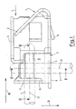
- the contact spring 1 has a connection end 2 and a contact end 3.
- a conductor In the area of the connection end 2 is a conductor, not shown, in the insertion direction 4 in the contact spring 1 insertable and contactable with this.
- the conductor is between the spring roof 5 and the terminal end 2 of the contact spring 1 held.
- the fixing tab bent out between the connection end 2 and the contact end 3 6 serves the fixing tab bent out between the connection end 2 and the contact end 3 6 for fixing the contact spring 1 in a connector housing.
- Further design details of the contact spring 1 and the introduction the contact spring 1 in a connector housing is expressly on the Contents of the aforementioned European patent application with the publication number 0 735 616. The entire revelation of the European The patent application should also apply expressly to the application here. It is expressly made to the disclosure of the European patent application Reference is made as far as the teaching of the local invention of the local disclosure not expressly opposed.
- the contact pin 7 is shown in dash-dotted lines. This is supposed to Expression come that the contact pin 7 by both on the bottom 8th the contact spring 1 arranged bottom opening 9 as well as through a on the spring back 10 attached back opening 11 in the socket area 12 of the Contact spring 1 is insertable.
- the contact pin 7, not shown in Fig. 2 is from the back 10 through the back opening 11 effective as insertion opening can be inserted into the socket.
- the bushing cavity 13 projects into the sheet metal tabs 14, 14 '.
- a guide groove 15 with a U-shaped cross section is formed in each of the sheet metal tabs 14, a guide groove 15 with a U-shaped cross section.
- the end faces 16 of the grooved legs 17, 17 ' serve as projections in the sense of the invention.
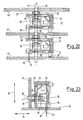
- the contact pin 7 is in the guide groove 15 of the grooved legs 17, 17 ' guided. Relative to an imaginary one that runs perpendicular to both sheet metal brackets
- the pivot plates 18, 14 ' are pivoted relative to one another by 90 °.
- the contact pin 7 shown there in a vertical Insertion direction 20 is inserted into the socket cavity 13, that is the central longitudinal axis 21 of the contact pin 7 there in the vertical insertion direction 20 runs, in this embodiment is that in the upper part of the figure illustrated sheet metal bracket 14 'formed guide groove 15 with its groove legs 17, 17 'act as a guide groove 15, while the end faces 16 of the opposite, on the sheet metal bracket 14 shown in the lower area of FIG. 3 serve as brake ribs to form a positive connection with the contact pin 7.
- Each of the guide grooves 15 thus has a double function.
- Corresponding run the central longitudinal axis 21 of the contact pin 7 and the other guide groove 15 perpendicular to each other, which leads to the end faces 16 of the groove legs 17, 17 'of the perpendicular to the central longitudinal axis 21 of the contact pin 7 Guide groove 15 are effective as brake ribs.
- the Guide groove 15 and the cylinder jacket of the contact pin 7 a frictional connection Holding the contact pin 7 in its insertion position in the socket cavity 13 out.
- the guide grooves 15 and in particular the end faces 16 of their groove legs 17, 17 'consequently have a double function according to the invention.
- FIGS. 4 and 5 a portion of the sheet metal tab 14 ' is bent out at right angles to form a back side 10.
- the back opening 11 is formed. Since the contact spring 1 is made of sheet metal, the back opening 11 is simply punched into the sheet metal part and afterwards bent by 90 ° relative to the sheet metal bracket 14. 4 can also be seen the guide groove 15 extending in the horizontal insertion direction 19.
- the contact spring 1 'shown in FIGS. 6 and 7 is in terms of its connection end 2 and the socket cavity 13 identical to that described above Contact spring 1 constructed according to FIG. 4. The only difference is that that at the bottom 8 as an additional contact element at right angles from the Underside 8 downward-facing solder pin 22 is formed. The solder pin 22 has thus in the vertical insertion direction 20.
- FIGS. 6 and 7 therefore relate to one Design of the contact spring 1 ', which is particularly suitable for this, with its underside 8 to be placed on a part to be connected.
- FIG. 10 finally shows the embodiment built into an insulating housing 23 the contact spring 1 according to FIG. 4.
- the contact spring 1 is by means of the fixing tab 6 fixed in the insulating housing 23.
- the insulating housing 23 has a conductor eye 24 through which a conductor not shown in the drawings in the insulating housing 23 can be inserted for contacting the terminal end 2 of the contact spring 1.
- the connector For contacting the connector can the connector with the help of the insulating housing bottom 25 also in Fig. 10 circuit board, not shown, are placed.
- the insulating housing 25 can then be a contact pin pointing in the vertical insertion direction 20 7 inserted through the housing bottom opening 26 into the socket cavity 13 become.
- a housing cover opening 30 on the housing top 29 Insert a contact pin 7 from the top 29 of the housing in a vertical direction Provide insertion direction 20.
- FIG. 11 shows one of three arranged one above the other in the vertical insertion direction 20 Isoliergeophusen 23 existing distributor 31.
- Isoliergeophusen 23 existing distributor 31 For arrangement one above the other stands in each case from the insulating housing underside 25 of each insulating housing 23 a stand 32 also.
- the contact mast 33 Enforced for contacting and fixing the position in the socket area the contact mast 33 all insulating housings 23 arranged one above the other or the socket cavities 13 of the contact springs lying in the insulating housings 23 1.
- the contact mast 33 thus replaces the contact pins 7 in the embodiments 1 to Fig. 10.
- the contact mast 33 is preferred designed in one piece and penetrates several connectors. To this The potential of the bottom or top connector is multiplied. Instead of only one conductor eye 24 there are three conductor eyes in the exemplary embodiment 24 of the same potential are available.
- the contact mast 33 penetrates here each insulating housing 23 both in its housing bottom opening 26 and in its housing cover opening 30 in the vertical insertion direction 20.
- Fig. 12 again shows an insulating housing 23 with one in a vertical Insertion direction 20 facing solder pin 22 provided contact spring 1 '.
- the insulating housing 23 with its insulating housing underside 25 can be placed on a component, for example a printed circuit board. Is putting on the Isoliergeophuses 23 with the back of the housing 27 desired, this is with the in Fig. 13 shown connector possible.
- Connector is in the insulating housing 23 that embodiment of the contact spring 1 '' integrated, with the solder pin 22 'in the horizontal insertion direction 19 protrudes from the rear of the housing 27.
- Fig. 14 is the embodiment of the connector shown in Fig. 12 shown again. It shows in addition to the details shown in FIG. 12 through the back opening 28 from the back of the housing 27
- Contact comb 34 introduced into the socket cavity 13.
- the contact comb 34 serves to bridge a plurality of contacts formed by contact springs 1 ' in the connector. 14 with the bottom of the insulating housing 25 in the final assembly state on a not shown in Fig. 14 PCB sits with which the connector by means of the vertical Insert direction 20 pointing solder pins 22 is connected, the contact comb 34 can also be freely installed with the connector placed on the circuit board and removable.
- the contact comb 34 simply from the housing side 25,27,29 into the socket cavity 13 introduced with which the connector sits on the circuit board. This is shown in FIG. 15. This is because there is the insulating housing 23 of the connector by means of the soldering pin 22 'pointing in the horizontal insertion direction 19 with the PCB connected. The connector is therefore with its rear side 27 on the circuit board, not shown. Because the contact comb 34 in turn introduced through the housing back opening 28 into the socket cavity 13 is, the contact comb 34 is, so to speak, through to the rear of the housing 27 adjacent circuit board closed.
- the contact comb 34 By means of the contact comb 34, it is possible to have all the socket contacts Connector either from the case back opening 28 or from the case bottom opening 26 or from the housing cover opening 30 together to bridge. Of course, it is also possible to select several To bridge socket contacts. It is also a so-called mixed assembly possible when bridging, in which selected contacts with a first bridging are bridged from the case back opening 28 and other contacts in turn with a second jumper from the housing cover opening 30 or the housing bottom opening 26 are bridged here. Of course it is also possible to have both bridged and unbridged contacts in summarize a connector.
- FIGS. 16 to 23 A further broad field of application of the invention is shown in FIGS. 16 to 23, namely the connection of several boards or printed circuit boards together.
- Fig. 16 shows a typical mother-daughter board connection. 16 extends in the horizontal insertion direction 19 a first circuit board, namely the motherboard 35. On the motherboard 35 is the insulating housing with its stand 32 23 of the connector. The construction of the connector corresponds to that Connector shown in Fig. 12. The solder pin 22 thus points in the vertical Insertion direction 20. The solder pin 22 is inserted into the circuit board bore 36 and soldered to it. The solder pin 22 thus forms the contact connection of the Connector to the motherboard 35.
- the daughter board 37 is used for 16 shows the housing back opening 28.
- the daughter board 37 is perpendicular to the mother board 35.
- the daughter board 37 thus extends in the vertical direction of insertion 20.
- the daughter board 37 is in turn from an insertion opening 38 breached. Inserted in the insertion opening 38 and - if desired - with you soldered the contact pin 7.
- the contact pin 7 engages mechanical and electrical coupling of the daughter board 37 through the back opening 28 into the socket area 12 of the contact spring 1 '.
- the connection between Contact pin 7 and the socket takes place as in connection with FIGS. 1 to Fig. 10 described.
- Between the daughter board 37 and the back of the case 27 is still the spacer ring used to stabilize the connector 39 a.
- FIG. 16 also clearly shows that they are not housing opening 26, 28, 30 - blocked by contact pin 7 or contact mast 33 16, the housing cover opening 30 - can be used as a test opening can. Through the housing cover opening 30, a contact element can easily Tester for testing purposes are introduced.
- the exemplary embodiment according to FIG. 17 shows the kinematic to a certain extent Inversion of the mother-daughter-board connection according to FIG. 16.
- the exemplary embodiment 17 again extend the daughter board 37 in vertical insertion direction 20 and at right angles to the mother board 35 in horizontal insertion direction 19.
- the insulating housing 23 set up with its stand 32 on the daughter board 37.
- the Solder pin 22 passes through a circuit board bore 36 'in the daughter board 37.
- the connector thus serves as a daughter board connector. Consequently, the contact pin 7 is in an insertion opening 38 ' fixed in the motherboard.
- it reaches through with a spacer ring 39 provided contact pin 7, the back opening 28 of the then vertical Connector. So with the mother-daughter-board connection can the connector both on the mother board 35 and on the daughter board 37 be arranged without this restricting the functionality of the connector.
- the housing cover opening 30 is in the embodiment 17 can be used for test purposes.
- FIG. 18 to 21 in turn show a contact spring according to FIG. 6 or the 12, but with different occupancy of the openings 26,28,30 the socket on the one hand and different orientations of the Mother board 35 and the daughter board 37 to each other on the other hand.
- Fig. 18 shows a parallel mother-daughter-board connection.
- the one arranged in the drawing below Mother board 35 runs like the one arranged above in the drawing Daughter board 37 with the connector plugged in horizontally Insertion direction 19.
- the Motherboard 35 the connector.
- the connector is with his Stand 32 on the motherboard 35 and is with its solder pin 22 in the motherboard 35 penetrating circuit board hole 36 soldered.
- the daughter board 37 is in turn penetrated by the contact pin in the insertion opening 38 7.
- the daughter board 37 rests with the interposition of the spacer ring 39 on the top of the housing 29 of the insulating housing 23.
- the contact pin 7 engages through the housing cover opening 30 in the socket.
- the case back opening 28 is consequently left free. It would of course be equally possible to place the connector on the daughter board Provide 37 and the motherboard 35 accordingly with the contact pin 7 to connect through the housing cover opening 30 with the connector. In the illustration in FIG. 18, only the insulating housing 23 of the plug connector would have to be used for this be rotated.
- FIG. 19 shows an arrangement of mother and daughter board according to FIG. 17.
- the contact is made using an angular contact pin, namely by means of the contact angle 40.
- the contact angle 40 engages again into an insertion opening 38 'in the motherboard 35 while the connector gets up with his stand 32 on the daughter board 37 and by means of Solder pins 22 penetrate the daughter board 37 in its circuit board bore 36 '.
- the exemplary embodiment 19 the case back opening 28 out of function and at the same time completely closed by the motherboard 35.
- the housing bottom opening 26 is closed accordingly by the daughter board 37.
- In the housing cover opening 30 is a leg of the contact angle 40 with the interposition of a spacer ring 39 inserted for contacting the motherboard 35 with the Daughter board 37.
- the mother board 35 extends in the horizontal insertion direction 19 and perpendicular to it the daughter board 37 in the vertical insertion direction 20.
- the connector is in the embodiment shown in FIG. 20 with the Motherboard 35 connected.
- the contact angle 40 is through the housing cover opening 30 inserted into the socket area 12 so that the housing back opening 28 is released, for example for testing purposes.
- the daughter board 37 is additionally fixed to the contact angle 40 by means of a fixing ring 41.
- Fig. 21 again shows the motherboard connector combination according to 20, but with the daughter board 37 running parallel to the mother board 35. Both boards run in the horizontal insertion direction 19.
- the coupling takes place through the back opening 28 by means of the contact angle 40, see above that the housing cover opening 30 is left free.
- the daughter board 37 attached to the contact bracket 40 by means of a fixing ring 41.
- a second fixing ring 41 for additional Stabilization of the connection is a second fixing ring 41 'in the area of Housing back opening 28 arranged.
- FIG. 22 A further embodiment is shown in FIG. 22.
- the same principle is used here as in the connector according to FIG. 11.
- Also in the embodiment according to 22 passes through a contact mast 33 a plurality of insulating housings 23 of connectors.
- In the embodiment of 22 are the lower and the middle board 42 each in the manner of a mother board educated.
- you carry in analogy to the exemplary embodiments in 16, 18, 20 and 21 each have an insulating housing 23.
- the insulating housing 23 stands thereby with its base 32 on the board 42.
- the connection between The connector and circuit board 42 are again made by soldering a solder pin 22 in a circuit board bore 36.
- the housing rear openings 28 are each left free.
- the contact mast 33 penetrates the insulating housings 23 in their housing bottom openings 26 or housing cover openings 30.
- the saddled in each case Circuit board 42 rests on a spacer ring 39 between circuit board 42 and the top of the housing 29.
- the modified embodiment can also be seen in the exemplary embodiment Board 42 '.
- the board 42 ' has only one insertion opening 38.
- the insertion opening the board 42 ' is simply plugged onto the contact mast 33.
- there is a direct plug connection between the contact mast 33 and the board 42 ' while in the case of the two lower boards 42 an indirect insertion or Contacting takes place by means of the arranged in the respective insulating housing 23 Rifle.
- Fig. 23 shows an example of the same embodiment as Fig. 16. However is in contrast to the embodiment of FIG. 16 in the embodiment 23 a contact spring according to FIG. 8 or a connector according to Fig. 15 used. In contrast to the exemplary embodiments shown in FIGS. 16 to 22 extends the solder pin 22 'in this embodiment parallel to the top of the housing 29 or to the bottom of the housing 25. The solder pin 22 ' is in the printed circuit board bore 36 which is in the horizontal insertion direction 19 extending motherboard 35 soldered.
- the stamped pattern 53 for the contact spring is from the metal sheet 52 1 ', 1' 'punched out.
- the individual punching patterns 53 are on the strips 54 molded.
- the strips 54 are used for production in the production direction 55 emotional.
- the punching pattern 53 point to the connection ends 2 which are to be bent later Contact springs 1 ', 1' 'and the solder pin 22, 22' to be bent if necessary.
- the sheet metal tab 14 with the guide groove sunk into it can be seen 15 and the insertion opening which later becomes the bottom opening 9.
- the contact spring 1 ', 1' ' the sheet metal tab 14 is simply around the bending edge 57 15 folded up from the drawing plane of FIG.
- the further sheet metal tab 14 'with the one assigned to it can also be seen Guide groove 15 and the insertion opening forming the later back opening 11.
- the sheet metal tab 14' is around the longitudinal bending edge 58 bent out of the drawing plane of FIG. 15 upwards. additionally becomes the area of the sheet metal tab which later has the back opening 11 14 'around the transverse bending edge 59 from the plane of the drawing in FIG. 15 folded up.
- solder pin 22, 22 ' is either left in its orientation as in the stamped pattern 53. However, if the solder pin should point vertically downwards from underside 8, the solder pin 22 'around the solder pin bending edge 61 downwards, that is into the Drawing plane of Fig. 15 bent away from the bottom 8.
- the advantage of the above-described stamping and bending technology is its easy automation, which is a cost-effective production of the contact spring 1,1 ', 1 "entails.
Landscapes
- Coupling Device And Connection With Printed Circuit (AREA)
Description
Die vorliegende Erfindung betrifft zunächst eine Steckbuchse und im weiteren Sinne eine mit einer erfindungsmäßigen Steckbuchse versehene Kontaktfeder sowie einen mit einer Kontaktfeder mit erfindungsmäßiger Steckbuchse versehenen elektrischen Steckverbinder.The present invention relates first to a socket and further Meaning a contact spring provided with an inventive socket and one provided with a contact spring with a socket according to the invention electrical connector.
Steckbuchsen als Elemente der Elektrotechnik sind beispielsweise bekannt aus BROCKHAUS, "Naturwissenschaften und Technik", Band A-EK, F.A. Brockhaus-Wiesbaden 1983, S. 183, ISBN 3-7653-0357-7. Sockets as elements of electrical engineering are known for example from BROCKHAUS, "Natural Sciences and Technology", Volume A-EK, FA Brockhaus-Wiesbaden 1983, p. 183, ISBN 3-7653-0357-7.
Bei nachfolgend kurz als Buchsen bezeichneten Steckbuchsen besteht zunächst das Problem, den nachfolgend als Kontaktstift bezeichneten Steckerstift in die Buchse einführen zu müssen. Nach dem Einstecken des Kontaktstifts in die Buchse besteht das Problem, daß der Kontaktstift einerseits gut und dauerhaft, also möglichst unverrückbar, in der Buchse gehalten sein muß, die Haltekräfte jedoch so bemessen sein müssen, daß der Kontaktstift jederzeit auch wieder aus der Buchse herausziehbar ist. Schließlich muß die Buchse noch so beschaffen sein, daß der Kontakt zwischen Kontaktstift und Buchse nicht durch ein mehrfaches Einführen und Entfernen des Kontaktstifts aus der Buchse sich verschlechtern darf.In the case of sockets, hereinafter referred to as sockets, there is first the problem, the connector pin referred to below as the contact pin in the Need to insert socket. After inserting the contact pin into the There is the problem that the contact pin, on the one hand, is good and durable, So immovable, must be held in the socket, the holding forces however, must be such that the contact pin can also be removed at any time the socket can be pulled out. Finally, the socket has to be procured be that the contact between the contact pin and socket is not a multiple Insertion and removal of the contact pin from the socket deteriorate may.
Aus der EP-A-0 701 299 ist eine zur Aufnahme von sowohl zylindrischen Kontaktstiften als auch flachen Kontaktsteckern geeignete Steckbuchse bekannt. Bei dieser Steckbuchse flankieren bei eingestecktem Kontaktstift bzw. Kontaktstecker zwei Kontaktflächen den Kontaktstift bzw. Kontaktstecker. Soweit die bekannte Steckbuchse zur Aufnahme zylindrischer Kontaktstifte dient, ist eine der Kontaktflächen als Führungsfläche und die andere Kontaktfläche als Reibfläche ausgestaltet. Die Führungsfläche ist hierbei mit Vorsprüngen zur formschlüssigen Führung des Kontaktstifts versehen, während die Reibfläche den Kontaktstift reibschlüssig in der Buchse fixiert.From EP-A-0 701 299 is one for receiving both cylindrical contact pins as well as flat contact plugs suitable socket known. at flank this socket when the contact pin or contact plug is inserted two contact surfaces the contact pin or contact plug. So far the known Socket for receiving cylindrical contact pins is one of the contact surfaces designed as a guide surface and the other contact surface as a friction surface. The guide surface is here with projections for positive guidance of the contact pin, while the friction surface frictionally engages the contact pin fixed in the socket.
Bei dieser bekannten Steckbuchse ist nachteilig, daß sie die Einführung des Kontaktstifts grundsätzlich in nur eine Steckrichtung ermöglicht. Diese Möglichkeit der Steckbarkeit in nur eine Richtung, verringert die Gebrauchsflexibilität der bekannten Steckbuchsen erheblich. Ist die Steckbuchse nämlich an einem prismatischen Teil vorgesehen, kann es beispielsweise erwünscht sein, dieses Teil sowohl in vertikaler als auch in horizontaler Anordnung einzubauen. Bei Verwendung der bekannten Steckbuchse müssen in diesem Fall zwei separate Steckbuchsentypen vorgesehen sein, um beide Montageorientierungen zu ermöglichen.In this known socket it is disadvantageous that it introduces the In principle, the contact pin allows only one plug-in direction. This possibility the pluggability in only one direction, reduces the flexibility of use of the known Sockets significantly. If the socket is on a prismatic Provided part, it may be desirable, for example, both this part to be installed in a vertical as well as in a horizontal arrangement. Using In this case, the known socket must have two separate types of socket be provided to allow both mounting orientations.
Ausgehend von den geschilderten Nachteilen liegt der Erfindung die Aufgabe zugrunde,
eine einfach aufgebaute, funktionssichere Steckbuchse mit verschiedenen
Steckrichtungen zu schaffen. Diese Aufgabe ist durch die Merkmalskombination
des Anspruches 1 in vorteilhafter und erfinderischer Weise gelöst.Starting from the disadvantages described, the invention is based on the object
a simply constructed, functionally reliable socket with different
To create plug directions. This task is due to the combination of features
of
Nach dem Oberbegriff des Anspruchs 1 sind in der Buchse zwei Kontaktflächen
vorgesehen, welche den Kontaktstift zwischen sich aufnehmen. Eine der beiden
Kontaktflächen ist als Führungsfläche wirksam. Hierfür sind auf der Führungsfläche
Vorsprünge vorgesehen, welche mit dem Kontaktstift eine formschlüssige
Führung ausbilden. Da der Kontaktstift beim Einführen in die Buchse in der Führung
geführt ist, ist ein leichtes Einstecken bzw. Herausziehen des Kontaktstifts
aus der Buchse gewährleistet.According to the preamble of
Zur Fixierung des eingeschobenen Kontaktstifts in seiner Einschubstellung ist die zweite Kontaktfläche als Reibfläche ausgebildet. Hierzu trägt sie ebenfalls Vorsprünge, welche mit dem Kontaktstift jedoch einen Reibschluß ausbilden. Dieser Reibschluß ist so gestaltet, daß die auf den Kontaktstift wirkenden Haltekräfte leicht durch die Handkraft beim Einschieben des Kontaktstifts überwunden werden können. Ein Verkanten des Kontaktstifts beim Einschieben ist durch die formschlüssige Führung auf der als Führungsfläche wirksamen anderen Kontaktfläche wirksam verhindert.To fix the inserted contact pin in its inserted position second contact surface formed as a friction surface. To this end, it also has protrusions, which, however, form a frictional connection with the contact pin. This Friction is designed so that the holding forces acting on the contact pin can be easily overcome by hand force when inserting the contact pin can. Tilting of the contact pin when inserting is due to the positive Leadership on the other contact surface effective as a guide surface effectively prevented.
Nach dem kennzeichnenden Teil des Anspruchs 1 bilden die Vorsprünge zusätzlich
auf jeder Kontaktfläche ein aus der Ebene der Kontaktfläche vorspringendes
Relief. Beide Reliefs sind identisch ausgebildet. Dies ist fertigungstechnisch günstig,
weil beide Reliefs prinzipiell mit ein- und demselben Werkzeug herstellbar
sind. Dies senkt die Werkzeugkosten.According to the characterizing part of
Die vorzugsweise einander parallel gegenüberstehenden Kontaktflächen sind bezüglich einer gedachten, beide Kontaktflächenebenen senkrecht durchdringenden Schwenkachse gegeneinander verschwenkt. Der Verschwenkungswinkel ist hierbei echt größer als 0° und echt kleiner als 180°. Die Mittellängsachsen der von den Relief-Vorsprüngen gebildeten Führungen verlaufen also in unterschiedliche Richtungen. Durch diesen unterschiedlichen Richtungsverlauf der Führungen auf den beiden Kontaktflächen ist auch jede dieser Richtungen als Einsteckrichtung für den Stecker nutzbar. Es ist evident, daß je Einsteckrichtung nur die Vorsprünge eines Reliefs einer Kontaktfläche als formschlüssige Führung mit dem Kontaktstift zusammenwirken können mit der Folge, daß die jeweils andere Führung inaktiv ist. Infolge der verschwenkten Stellung der Kontaktflächen gegeneinander bilden die Vorsprünge des Reliefs der jeweils inaktiven Führung mit dem Kontaktstift einen Reibschluß. Mit der Erfindung ist es folglich möglich, eine Buchse so zu gestalten, daß mit einer Buchse zwei Steckrichtungen realisierbar sind, wobei jeweils eine Kontaktfläche als Führungsfläche und die nicht als Führungsfläche wirksame Kontaktfläche als Reibfläche wirksam sind. Die Reliefs auf den Kontaktflächen haben somit eine erfinderische Doppelfunktion. The preferably mutually parallel contact surfaces are related an imaginary, perpendicularly penetrating both contact surface levels Swivel axis pivoted against each other. The pivot angle is here really bigger than 0 ° and really smaller than 180 °. The central longitudinal axes of The guides formed in the relief projections thus run in different ways Directions. Due to this different direction of the guides The two contact surfaces are each of these directions as the insertion direction usable for the plug. It is evident that only the projections per insertion direction a relief of a contact surface as a form-fitting guide with the contact pin can cooperate with the result that the other leadership is inactive. As a result of the pivoted position of the contact surfaces against one another form the projections of the relief of the inactive guide with the contact pin a frictional connection. With the invention it is therefore possible to use a socket to design that two plug directions can be realized with a socket, wherein one contact surface each as a guide surface and not as a guide surface effective contact surface are effective as a friction surface. The reliefs on the contact areas thus have an inventive double function.
Die rückbezogenen Ansprüche betreffen teilweise für sich selbst erfinderische und
teilweise zweckmäßige Weiterbildungen der im Anspruch 1 beanspruchten Erfindung.The back claims relate in part to inventive and self-inventing
partially useful developments of the invention claimed in
Nach der Lehre des Anspruchs 2 sind die Reliefs und damit die beiden Kontaktflächen
um die gedachte Schwenkachse mit einem Versatz von 90° gegeneinander
verschwenkt. Die beiden mit der Buchse realisierbaren Steckrichtungen verlaufen
exakt senkrecht zueinander. Bezogen auf ein gedachtes, rechteckiges Buchsengehäuse
bedeutet dies, daß der Kontaktstift in der einen Steckrichtung von der
Gehäuserückseite in Richtung auf die Gehäusevorderseite bzw. von der Gehäusevorderseite
in Richtung auf die Gehäuserückseite eingeschoben werden kann,
während er in der anderen Steckrichtung von der Gehäuseunterseite in Richtung
auf die Gehäuseoberseite bzw. von der Gehäuseoberseite in Richtung auf die Gehäuseunterseite
eingeschoben werden kann. Dies bedeutet, daß bei einer entsprechenden
Anzahl von Öffnungen das gedachte Gehäuse von jeder seiner Seiten
her mittels eines Kontaktstifts kontaktierbar ist.According to the teaching of
Mittels der erfindungsmäßigen Buchse ist es also möglich, ein Standardgehäuse für ein elektrisches Anschlußteil vorzukonfektionieren, welches in zahlreichen Relativstellungen an einem entsprechenden, mit einem Kontaktstift versehenen elektrischen Bauteil angeschlossen werden kann. Eine Vielzahl von Einbaustellungen des mit der erfindungsmäßigen Buchse versehenen Teils gegenüber dem entsprechenden, mit dem Kontaktstift versehenen Teil sind also auf konstruktiv sehr einfachem Weg realisierbar.By means of the socket according to the invention it is therefore possible to have a standard housing prefabricated for an electrical connector, which in numerous Relative positions on a corresponding one, provided with a contact pin electrical component can be connected. A variety of mounting positions of the part provided with the inventive socket compared to the corresponding part provided with the contact pin are thus constructive very easy way.
Anspruch 3 betrifft eine konstruktiv einfache und dadurch kostengünstig herstellbare
Geometrie des Reliefs. Das Relief ist hierbei als V- bzw. U-förmige Führungsnut
ausgestaltet, wobei die Stirnseiten der beiden Nutschenkel aus der Ebene
der Kontaktfläche vorspringen und so als Vorsprünge im Sinne der Erfindung
wirksam sind. Das so gestaltete Relief bewirkt, daß der in Mittellängsrichtung der
Führungsnut eingeführte Kontaktstift mit der Nut eine offene Bahnführung ausbildet,
während die Stirnseiten der Nutschenkel der inaktiven Nut auf der anderen
Kontaktfläche nach Art zweier paralleler Bremsrippen in Richtung auf den Kontaktstift
vorstehen und so den Kontaktstift reibschlüssig halten. Infolge der Reibung
des Kontaktstifts an den Stirnseiten der Nutschenkel der inaktiven Führungsnut
wird der Kontaktstift beim Einstecken selbsttätig von Verschmutzungen
bzw. Korrosionsrückständen gereinigt, so daß stets ein guter elektrischer Kontakt
zwischen Kontaktstift und Buchse gewährleistet ist.
Besonders vorteilhaft ist die Verwendung von Blech als Buchsenmaterial nach
Anspruch 4, in welches die vorzugsweise als Führungsnuten ausgebildeten Reliefs
einfach als Sicken eingeformt werden können. Außerdem können so beide
Kontaktflächen federnd ausgebildet werden zur Verbesserung sowohl des mechanischen
als auch des elektrischen Kontakts mit dem eingeschobenen Kontaktstift.
Besonders kostengünstig herstellbar ist die Buchse mit Hilfe eines
Stanzbiegeverfahrens, wie es in Anspruch 5 angegeben ist. Hierbei kann das gesamte
für die Buchse erforderliche Material aus einer Blechtafel ausgestanzt werden
und anschließend durch entsprechendes Umformen in die gewünschte Geometrie
gebracht werden.The use of sheet metal as the bushing material is particularly advantageous
Claim 4, in which the reliefs preferably formed as guide grooves
can simply be molded as beads. In addition, both can
Contact surfaces are resilient to improve both the mechanical
as well as the electrical contact with the inserted contact pin.
The socket can be produced particularly cost-effectively with the aid of a
Stamping and bending process as specified in
Zur Verbesserung der lösungsgemäßen Eigenschaften der Buchse ist es vorteilhaft,
als zusätzliche Führung eine in ihrer Querschnittsform an die Geometrie des
Kontaktstifts angepaßte Einführöffnung vorzusehen, wie in Anspruch 6 beansprucht.
Der Kontaktstift ist beim Einführen dann zunächst in der als Führungsauge
wirksamen Einführöffnung geführt. Die Einführöffnung ergänzt die vorbeschriebene
offene Bahnführung zu einer teilweise geschlossenen Bahnführung. Das
Einführen des Kontaktstifts ist auf diese Weise zusätzlich erleichtert. Insbesondere
ist ein Verkanten des Kontaktstifts in der Buchse und damit ein ungewünschtes
Ausleiern der Buchse zusätzlich verhindert. Außerdem ist die Schnittstelle zwischen
Kontaktstift und Buchse mittels der Einführöffnung zusätzlich abgesichert,
was ungewollte Spannungsüberschläge oder Kriechströme zusätzlich verhindert. To improve the properties of the socket according to the solution, it is advantageous
as an additional guide in its cross-sectional shape to the geometry of the
Provide contact pin adapted insertion opening as claimed in
Die Ansprüche 7 und 8 betreffen stringente Weiterbildungen der in Anspruch 5
erwähnten Stanzbiegetechnik. Hierbei sind die Einführöffnungen neben den Kontaktflächen
in Blechlaschen einfach eingestanzt. Im Fertigungsendzustand der
Buchse ist der Bereich mit der eingestanzten Einführöffnung dann einfach gegenüber
der benachbarten Kontaktfläche rechtwinklig abgebogen. Die Anordnung
einer Einführöffnung neben der bezogen auf diese Einführöffnung als Reibfläche
wirksamen Kontaktfläche ist platzsparend, weil die Führungsnut sehr nah an der
Einführöffnung angebracht werden kann. Durch einfaches Biegen der einzelnen
Bereiche der Blechtafel können die Einführöffnungen und Führungsnuten in die
gewünschte Relativstellung zueinander umgeformt werden. Diese Herstellung ist
einfach automatisierbar und damit kostengünstig.
Anspruch 10 betrifft die synergistische Wirkung der vorbeschriebenen Einzelmerkmale.
Nach der Lehre des Anspruchs 10 weist die dort beanspruchte Ausführungsform
der erfindungsmäßigen Buchse zwei an die Außengeometrie des jeweiligen
Kontaktstifts angepaßte Einführöffnungen auf. Mit jeder Einführöffnung
wirken jeweils eine Führungsfläche und eine gegenüberliegende Reibfläche zusammen.
Mit der dort beanspruchten Steckbuchse ist es also möglich, in zwei
rechtwinklig zueinander stehenden Einsteckrichtungen das mit der Buchse versehene
elektrische Bauteil zu kontaktieren.
Anspruch 11 betrifft eine weitere Ausführungsform der Steckbuchse mit einem
oder mehreren zusätzlichen, an mindestens eine Blechlasche angeformten Kontaktelementen.
Ein solches Kontaktelement kann beispielsweise ein Lötpin sein,
zum Anschluß des mit der Buchse versehenen Geräts an eine Leiterplatte oder
ein anderes Gerät. Das zusätzliche Kontaktelement dient dann gewissermaßen
als Primäranschluß. Die noch verbliebenen, ungenutzten erfindungsmäßigen
Buchsen können als Sekundäranschlüsse beispielsweise zur Parallelschaltung
oder zur Brückung mehrerer mit den erfindungsmäßigen Buchsen versehener Geräte
dienen. Hierbei können die einzelnen Geräte unterschiedlich zueinander orientiert
sein, was infolge der Variabilität der erfindungsmäßigen Steckbuchse einfach
möglich ist.
Die Ansprüche 12 und 13 betreffen eine an sich aus der am 02. Oktober 1996
veröffentlichten europäischen Patentanmeldung mit der Veröffentlichungsnummer
EP-A-0 735 616 bekannte Kontaktfeder für einen elektrischen Steckverbinder.
Diese am 01. April 1996 angemeldete europäische Patentanmeldung mit der Anmeldenummer
96 105 169.5 geht auf die hiesige Anmelderin zurück. Die in den
Ansprüchen 12 und 13 beanspruchte Kontaktfeder gleicht in ihrem Aufbau hinsichtlich
ihres Anschlußendes der aus der europäischen Patentanmeldung bekannten
Kontaktfeder. Bei der Kontaktfeder nach Anspruch 12 ist im Gegensatz
zur genannten europäischen Patentanmeldung die hier beanspruchte Buchse als
Buchsenkontakt am Kontaktende zum direkten Steckanschluß wirksam. Nach Anspruch
13 dient das aus Anspruch 11 bekannte zusätzliche Kontaktelement als
Anschluß am Kontaktende der Kontaktfeder, während die Steckbuchse bzw. die
Steckbuchsen lediglich zur Aufnahme zusätzlicher Kontaktstücke, beispielsweise
eines zusätzlichen Brückungskontakts in Form eines Kontaktkamms, dient.
Die Ansprüche 14 und 15 betreffen schließlich den gesamten, aus der vorerwähnten
europäischen Patentanmeldung an sich bekannten elektrischen Steckverbinder.
Nach Anspruch 14 dient die erfindungsmäßige Steckbuchse der hiesigen Erfindung
beim bekannten Steckverbinder als Kontaktende, um den Steckverbinder
mittels der in der europäischen Patentanmeldung vorbeschriebenen direkten
Stecktechnik auf einer Leiterplatte steckend fixieren zu können.Finally, claims 14 and 15 relate to the whole of the aforementioned
European patent application known electrical connector.
According to
Nach der Lehre des Anspruchs 15 dient wiederum das in Anspruch 11 beanspruchte
zusätzliche Kontaktelement als Lötpin zur Steckverbinderfixierung mittels
direkter Stecktechnik auf der Leiterplatte. Die erfindungsmäßige Steckbuchse
dient bei dieser Ausführungsform wiederum zur Aufnahme weiterer Kontaktstücke,
beispielsweise einer Zinke eines Kontaktkamms. Mit Hilfe eines Kontaktkamms
lassen sich mehrere Steckverbinderkontakte miteinander brücken. Diese Brükkung
ist beispielsweise erforderlich, um mehrere Schutzleiterkontakte miteinander
zu verbinden, weil eine elektrische Verbindung von Schutzleiterkontakten über
Leiterzüge einer Leiterplatte aus sicherheitstechnischen Gründen nicht möglich
bzw. durch entsprechende Normen untersagt ist. Auch ist es natürlich möglich,
mehrere Kontakte eines Steckverbinders mit Hilfe eines Kontaktkamms parallel zu
schalten bzw. in Serie zu schalten. Auch ist es möglich durch das Vorhandensein
zweier senkrecht zueinander stehender Buchsenkontakte verschiedene Buchsen
unabhängig voneinander zu brücken, also eine Mischbestückung durch unterschiedliche
Brückungen vorzusehen.According to the teaching of
Die miteinander fluchtenden Öffnungen in der Isoliergehäuseunterseite und der Isoliergehäuseoberseite nach Anspruch 16 erlauben es, durch den Steckverbinder bzw. das Steckverbindergehäuse einen langen, als Kontaktmast bezeichneten Kontaktstift hindurchzustecken. Auf diese Weise ist es möglich, mehrere Steckverbinder übereinander nach Art eines Verteilers anzuordnen oder mehrere mit Platinen bzw. Leiterplatten verbundene Steckverbinder so zu verbinden, daß eine Mehrfachverbindung von Leiterplatten entsteht. Hierbei können die Leiterplatten selbst auf den Kontaktmast aufgesteckt sein bzw. der Kontaktmast durch auf den Leiterplatten fixierte Steckverbinder hindurchgesteckt sein.The aligned openings in the bottom of the insulating housing and the Insulating housing top according to claim 16 allow through the connector or the connector housing has a long, referred to as a contact mast Insert the contact pin. In this way it is possible to have multiple connectors to be arranged one above the other in the manner of a distributor or several with To connect boards or printed circuit boards connected connectors so that a Multiple connection of printed circuit boards is created. Here, the circuit boards be plugged onto the contact mast itself or the contact mast through onto the Printed circuit board-fixed connectors can be inserted.
Anspruch 17 betrifft schließlich die Verwendung des Steckverbinders auf einer
Leiterplatte als Schnittstelle zur Schaffung einer Mutter-Tochter-Platinenverbindung.
Mit der Erfindung ist es also möglich, mehrere Platinen miteinander
zu verbinden. Schließlich ist es bei vielen Ausführungsformen vorteilhaft, daß eine
Einführöffnung für die Buchse nicht benötigt ist, so daß ein Kontaktelement eines
Prüfgerätes eingeführt werden kann, so daß die an sich überflüssige Öffnung als
Prüföffnung nutzbar ist.
Anhand der in den Zeichnungen dargestellten Ausführungsbeispiele ist die Erfindung näher beschrieben. Es zeigen:
- Fig. 1
- eine geschnittene Seitenansicht einer Kontaktfeder mit erfindungsmäßiger Steckbuchse und gestrichelt gezeichnet zwei Möglichkeiten zur Einführung jeweils eines Kontaktstifts,
- Fig. 2
- den Schnitt II-II in Fig. 1,
- Fig. 3
- den Schnitt III-III in Fig. 1,
- Fig. 4
- eine Seitenansicht einer Kontaktfeder ohne zusätzliches Kontaktelement,
- Fig. 5
- eine Draufsicht auf die Rückseite der Kontaktfeder gemäß Pfeil V in Fig. 4,
- Fig. 6
- eine Seitenansicht einer Kontaktfeder mit einem nach unten abgebogenen zusätzlichen Kontaktelement,
- Fig. 7
- eine Draufsicht auf die Rückseite der Kontaktfeder gemäß Pfeil VII in Fig. 6,
- Fig. 8
- eine Seitenansicht einer Kontaktfeder mit einem nach hinten abstehenden zusätzlichen Kontaktelement,
- Fig. 9
- eine Ansicht auf die Unterseite der Kontaktfeder gemäß Pfeil IX in Fig. 8,
- Fig. 10
- eine Seitenansicht einer in ein Steckverbindergehäuse eingesetzten Kontaktfeder gemäß Fig. 4,
- Fig. 11
- einen aus drei Steckverbindergehäusen gemäß Fig. 10 zusammengesetzten Verteiler,
- Fig. 12
- eine Seitenansicht einer in ein Steckverbindergehäuse eingesetzten Kontaktfeder gemäß Fig. 6,
- Fig. 13
- eine Seitenansicht einer in ein Steckverbindergehäuse eingesetzten Kontaktfeder gemäß Fig. 8,
- Fig. 14
- eine Schnittdarstellung eines Steckverbinders gemäß Fig. 11 mit einem senkrecht zum zusätzlichen Kontaktelement verlaufenden Kontaktkamm zum Zwecke der Brückung,
- Fig. 15
- eine Schnittdarstellung eines Steckverbinders gemäß Fig. 12 mit einem parallel zum zusätzlichen Kontaktelement verlaufenden Kontaktkamm zum Zwecke der Brückung,
- Fig. 16
- einen auf einer Mutterplatine angebrachten Steckverbinder gemäß Fig. 12 mit senkrecht dazu angebrachter Tochterplatine,
- Fig. 17
- einen auf einer Tochterplatine angebrachten Steckverbinder gemäß Fig. 12 mit einer senkrecht dazu angebrachten Mutterplatine,
- Fig. 18
- einen auf einer Mutterplatine angebrachten Steckverbinder gemäß Fig. 12 mit einer parallel zur Mutterplatine angebrachten Tochterplatine,
- Fig. 19
- einen auf einer Tochterplatine angebrachten Steckverbinder gemäß Fig. 12 mit einer senkrecht dazu angebrachten Mutterplatine mit einem zwischen Steckverbinder und Mutterplatine wirksamen Kontaktwinkel,
- Fig. 20
- einen auf einer Mutterplatine angebrachten Steckverbinder gemäß Fig. 12 mit senkrecht dazu angebrachter Tochterplatine und mit einem zwischen Tochterplatine und Steckverbinder wirksamen Kontaktwinkel,
- Fig. 21
- einen auf einer Mutterplatine angebrachten Steckverbinder gemäß Fig. 12 mit parallel dazu angebrachter Tochterplatine und mit einem Kontaktwinkel zwischen Tochterplatine und Steckverbinder,
- Fig. 22
- eine aus drei Platinen bestehende Mehrfachverbindung mit zwei Steckverbindern gemäß Fig. 12
- Fig. 23
- einen auf einer Mutterplatine angebrachten Steckverbinder gemäß Fig. 13 mit einer senkrecht dazu verlaufenden, am Steckverbinder angeschlossenen Tochterplatine
- Fig. 24
- zwei Blech-Stanzzuschnitte der Kontaktfedern gemäß Fig. 6 bzw. Fig. 8 vor dem Biegen.
- Fig. 1
- 2 shows a sectional side view of a contact spring with a socket according to the invention and drawn in broken lines, two options for introducing a contact pin in each case,
- Fig. 2
- the section II-II in Fig. 1,
- Fig. 3
- the section III-III in Fig. 1,
- Fig. 4
- a side view of a contact spring without additional contact element,
- Fig. 5
- a plan view of the back of the contact spring according to arrow V in Fig. 4,
- Fig. 6
- 2 shows a side view of a contact spring with an additional contact element bent downwards,
- Fig. 7
- a plan view of the back of the contact spring according to arrow VII in Fig. 6,
- Fig. 8
- 2 shows a side view of a contact spring with an additional contact element projecting towards the rear,
- Fig. 9
- a view of the underside of the contact spring according to arrow IX in Fig. 8,
- Fig. 10
- 3 shows a side view of a contact spring according to FIG. 4 inserted into a connector housing,
- Fig. 11
- a distributor composed of three connector housings according to FIG. 10,
- Fig. 12
- 6 shows a side view of a contact spring according to FIG. 6 inserted into a connector housing,
- Fig. 13
- 8 shows a side view of a contact spring according to FIG. 8 inserted into a connector housing,
- Fig. 14
- 11 shows a sectional view of a connector according to FIG. 11 with a contact comb running perpendicular to the additional contact element for the purpose of bridging,
- Fig. 15
- 12 shows a sectional view of a connector according to FIG. 12 with a contact comb running parallel to the additional contact element for the purpose of bridging,
- Fig. 16
- 12 with a daughter board attached perpendicular to it,
- Fig. 17
- 12 with a mother board mounted perpendicular to it,
- Fig. 18
- 12 with a daughter board attached parallel to the mother board,
- Fig. 19
- 12 with a mother board mounted perpendicular to it with an effective contact angle between the connector and mother board,
- Fig. 20
- 12 with a daughter board attached perpendicular to it and with a contact angle effective between the daughter board and the connector,
- Fig. 21
- 12 with a daughter board attached in parallel and with a contact angle between daughter board and connector,
- Fig. 22
- a multiple connection consisting of three circuit boards with two connectors according to FIG. 12
- Fig. 23
- a connector attached to a mother board according to FIG. 13 with a daughter board running perpendicular to it and connected to the connector
- Fig. 24
- two sheet metal die cuts of the contact springs according to FIG. 6 or FIG. 8 before bending.
Die Kontaktfeder 1 weist ein Anschlußende 2 und eine Kontaktende 3 auf. Im Bereich
des Anschlußendes 2 ist ein nicht dargestellter Leiter in Einführrichtung 4 in
die Kontaktfeder 1 einführbar und mit dieser kontaktierbar. Der nicht dargestellte
Leiter ist bei dieser Ausführungsform zwischen dem Federdach
5 und dem Anschlußende 2 der Kontaktfeder 1 gehalten. Schließlich dient
der zwischen dem Anschlußende 2 und dem Kontaktende 3 ausgebogene Fixierlappen
6 zur Fixierung der Kontaktfeder 1 in einem Steckverbindergehäuse. Hinsichtlich
weiterer konstruktiver Einzelheiten der Kontaktfeder 1 bzw. der Einbringung
der Kontaktfeder 1 in ein Steckverbindergehäuse sei ausdrücklich auf den
Inhalt der vorerwähnten europäischen Patentanmeldung mit der Veröffentlichungsnummer
0 735 616 verwiesen. Die gesamte Offenbarung der europäischen
Patentanmeldung soll auch ausdrücklich für die hiesige Anmeldung gelten. Es
wird also auf die Offenbarung der europäischen Patentanmeldung ausdrücklich
Bezug genommen, soweit die Lehre der hiesigen Erfindung der dortigen Offenbarung
nicht ausdrücklich entgegensteht.The
In Fig. 1 ist der Kontaktstift 7 jeweils strichpunktiert dargestellt. Dadurch soll zum
Ausdruck kommen, daß der Kontaktstift 7 sowohl durch eine auf der Unterseite 8
der Kontaktfeder 1 angeordnete Bodenöffnung 9 als auch durch eine an der Feder-Rückseite
10 angebrachte Rückenöffnung 11 in den Buchsenbereich 12 der
Kontaktfeder 1 einführbar ist.In Fig. 1, the
Der in Fig. 2 nicht dargestellte Kontaktstift 7 ist von der Rückseite 10 her durch die
als Einführöffnung wirksame Rückenöffnung 11 in die Buchse einführbar. In den
Buchsenhohlraum 13 ragen hinein die Blechlaschen 14, 14'. In jede der Blechlaschen
14 ist eine im Querschnitt U-förmige Führungsnut 15 eingeformt. Die Stirnseiten
16 der Nutschenkel 17,17' dienen hierbei als Vorsprünge im Sinne der Erfindung.
Der Kontaktstift 7 ist in der Führungsnut 15 von den Nutschenkeln 17,17'
geführt. Bezogen auf eine gedachte, zu beiden Blechlaschen senkrecht verlaufende
Schwenkachse 18 sind die Blechlaschen 14,14' gegeneinander um 90° verschwenkt.
Während die Führungsnut 15 der in Fig. 2 rechts abgebildeten Blechlasche
14 in waagrechter Einschubrichtung 19 verläuft, verläuft die entsprechende
Führungsnut 15 der in Fig. 2 links dargestellten Blechlasche in senkrechter Einschubrichtung
20. Die Führungsnuten 15 der beiden Blechlaschen 14,14' verlaufen
folglich rechtwinklig zueinander. Die Stirnseiten 16 der Führungsnut 15 der in
Fig. 2 links dargestellten Blechlasche 14 verlaufen folglich rechtwinklig zur Mittellängsachse
21 des in Fig. 2 in waagrechter Einschubrichtung 19 eingeschobenen
Kontaktstifts 7 und sind somit als Bremsrippen wirksam. Die Stirnseiten 16 der
Führungsnut 15 der in Fig. 2 links dargestellten Blechlasche 14' bilden zusammen
mit dem Kontaktstift 7 einen Reibschluß aus zur Steckfixierung des Kontaktstifts 7
im Buchsenhohlraum 13.The
Entsprechend sind die Funktionen der Blechlaschen 14,14' in der Darstellung der
Fig. 3 gegenüber der Darstellung in Fig. 2 vertauscht. In der Darstellung der Fig. 3
entspricht die im oberen Bereich der Figur abgebildete Blechlasche 14' der in
Fig. 2 links abgebildeten Blechlasche 14'. Entsprechend ist die im unteren Teil der
Fig. 3 abgebildete Blechlasche 14 identisch mit der im rechten Teil der Fig. 2 abgebildeten
Blechlasche 14. Da in Fig. 3 der dort abgebildete Kontaktstift 7 in senkrechter
Einschubrichtung 20 in den Buchsenhohlraum 13 eingeschoben ist, also
die Mittellängsachse 21 des Kontaktstifts 7 dort in senkrechter Einschubrichtung
20 verläuft, ist bei dieser Ausführungsform die in die im oberen Teil der Figur
abgebildete Blechlasche 14' eingeformte Führungsnut 15 mit ihren Nutschenkeln
17,17' als Führungsnut 15 wirksam, während die Stirnseiten 16 der gegenüberliegenden,
an der im unteren Bereich der Fig. 3 dargestellten Blechlasche 14
als Bremsrippen zur Ausbildung eines Formschlusses mit dem Kontaktstift 7 dienen.The functions of the
Jede der Führungsnuten 15 hat also eine Doppelfunktion. Verlaufen die Mittellängsachse
21 des Kontaktstifts 7 und die Führungsnut 15 in derselben Einschubrichtung,
bilden der Zylindermantel des Kontaktstifts 7 und die Führungsnut
15 eine formschlüssige offene Bahnführung miteinander aus. Entsprechend
verlaufen die Mittellängsachse 21 des Kontaktstifts 7 und die andere Führungsnut
15 senkrecht zueinander, was dazu führt, daß die Stirnseiten 16 der Nutschenkel
17,17' der senkrecht zur Mittellängsachse 21 des Kontaktstifts 7 verlaufenden
Führungsnut 15 als Bremsrippen wirksam sind. In diesem Fall bilden die
Führungsnut 15 und der Zylindermantel des Kontaktstifts 7 einen Reibschluß zur
Halterung des Kontaktstifts 7 in seiner Einschubstellung im Buchsenhohlraum 13
aus. Die Führungsnuten 15 und insbesondere die Stirnseiten 16 ihrer Nutschenkel
17,17' haben nach der Erfindung folglich eine Doppelfunktion.Each of the
Aus den Fig. 4 und Fig. 5 ist erkennbar, daß von der Blechlasche 14' ein Teilbereich
rechtwinklig ausgebogen ist zur Bildung einer Rückseite 10. In die Rückseite
10 ist die Rückenöffnung 11 eingeformt. Da die Kontaktfeder 1 aus Blech besteht,
ist die Rückenöffnung 11 einfach in das Blechteil eingestanzt und hinterher
gegenüber der Blechlasche 14 um 90° abgebogen. In Fig. 4 ist weiterhin erkennbar
die in waagrechter Einschubrichtung 19 verlaufende Führungsnut 15.It can be seen from FIGS. 4 and 5 that a portion of the sheet metal tab 14 '
is bent out at right angles to form a
Die in den Fig. 6 und 7 dargestellte Kontaktfeder 1' ist hinsichtlich ihres Anschlußendes
2 und des Buchsenhohlraums 13 identisch mit der vorbeschriebenen
Kontaktfeder 1 gemäß Fig. 4 aufgebaut. Sie unterscheidet sich lediglich dadurch,
daß an die Unterseite 8 als zusätzliches Kontaktelement der rechtwinklig aus der
Unterseite 8 nach unten weisende Lötpin 22 angeformt ist. Der Lötpin 22 weist
also in die senkrechte Einschubrichtung 20. Fig. 6 und 7 betreffen also eine
Bauform der Kontaktfeder 1', welche besonders dafür geeignet ist, mit ihrer Unterseite
8 auf ein anzuschließendes Teil aufgesetzt zu werden.The contact spring 1 'shown in FIGS. 6 and 7 is in terms of its
Besteht das Bedürfnis, die Kontaktfeder 1' auf ihrer Rückseite 10 mittels eines
Lötpins 22 auf ein weiteres Teil kontaktierend aufzusetzen, eignet sich hierfür die
in den Fig. 8 und 9 dargestellte Ausführungsform der Kontaktfeder 1". Bei der
Kontaktfeder 1'' weist der Lötpin 22' in waagrechter Einschubrichtung 19 parallel
zur Unterseite 8 verlaufend aus der Rückseite 10 heraus.There is a need to contact spring 1 'on its
Fig. 10 zeigt schließlich die in ein Isoliergehäuse 23 eingebaute Ausführungsform
der Kontaktfeder 1 gemäß Fig. 4. Die Kontaktfeder 1 ist mit Hilfe des Fixierlappens
6 im Isoliergehäuse 23 ortsfest fixiert. Das Isoliergehäuse 23 weist ein Leiterauge
24 auf, durch welches ein in den Zeichnungen nicht dargestellter Leiter in
das Isoliergehäuse 23 eingeschoben werden kann zur Kontaktierung mit dem Anschlußende
2 der Kontaktfeder 1. Zur Kontaktierung des Steckverbinders kann
der Steckverbinder mit Hilfe der Isoliergehäuseunterseite 25 auf eine ebenfalls in
Fig. 10 nicht dargestellte Leiterplatte aufgesetzt werden. In die Isoliergehäuseunterseite
25 kann dann ein in senkrechter Einschubrichtung 20 weisender Kontaktstift
7 durch die Gehäusebodenöffnung 26 in den Buchsenhohlraum 13 eingeschoben
werden. Analog dazu kann durch die in der Gehäuserückseite 27 vorgesehene
Gehäuserückenöffnung 28 ein Kontaktstift 7 in waagrechter Einschubrichtung
19 in den Buchsenhohlraum 13 eingeschoben werden. Ebensogut ist es jedoch
auch möglich, im Isoliergehäuse 23 des Steckverbinders lediglich entweder
eine Gehäusebodenöffnung 26 oder eine Gehäuserückenöffnung 28 vorzusehen.
Damit ist die Einschubrichtung 19,20 für den Kontaktstift 7 von vornherein fest
definiert. Auf diese Weise kann nach Art einer Kodierung verhindert werden, daß
das Isoliergehäuse 23 des Steckverbinders in einer falschen Orientierung, beispielsweise
auf eine Leiterplatte aufgesetzt wird. Vorteilhaft ist hierbei, daß dieselbe
Ausführungsform der Kontaktfeder 1 sowohl für die waagrechte Einschubrichtung
19 als auch für die senkrechte Einschubrichtung 20 verwendet
werden kann. Ist nämlich die Gehäusebodenöffnung 26 bzw. die Gehäuserükkenöffnung
28 veschlossen, ist auch die entsprechend zugeordnete Bodenöffnung
9 bzw. Rückenöffnung 11 der Kontaktfeder 1 deaktiviert. Schließlich ist es
auch möglich, auf der Gehäuseoberseite 29 eine Gehäusedeckelöffnung 30 zum
Einschieben eines Kontaktstifts 7 von der Gehäuseoberseite 29 her in senkrechter
Einschubrichtung 20 vorzusehen.10 finally shows the embodiment built into an insulating
Fig. 11 zeigt einen aus drei in senkrechter Einschubrichtung 20 übereinander angeordneten
Isoliergehäusen 23 bestehenden Verteiler 31. Zur Anordnung übereinander
steht jeweils aus der Isoliergehäuseunterseite 25 eines jeden Isoliergehäuses
23 ein Standfuß 32 hinaus. Bei der Anordnung der Isoliergehäuse 23
übereinander steht jeweils auf der Gehäuseoberseite 29 des darunter angeordneten
Isoliergehäuses 23 der Standfuß 32 des jeweils darüber angeordneten Isoliergehäuses
23 auf. Zur Kontaktierung und Lagefixierung im Buchsenbereich durchsetzt
der Kontaktmast 33 sämtliche übereinander angeordneten Isoliergehäuse 23
bzw. die Buchsenhohlräume 13 der in den Isoliergehäusen 23 einliegenden Kontaktfedem
1. Der Kontaktmast 33 ersetzt folglich die Kontaktstifte 7 bei den Ausführungsformen
gemäß Fig. 1 bis Fig. 10. Der Kontaktmast 33 ist vorzugsweise
einstückig ausgestaltet und durchsetzt eben mehrere Steckverbinder. Auf diese
Weise ist das potential des untersten bzw. obersten Steckverbinders vervielfacht.
Anstelle nur eines Leiterauges 24 stehen beim Ausführungsbeispiel drei Leiteraugen
24 desselben Potentials zur Verfügung. Der Kontaktmast 33 durchsetzt hierbei
jedes Isoliergehäuse 23 sowohl in seiner Gehäusebodenöffnung 26 als auch
in seiner Gehäusedeckelöffnung 30 in senkrechter Einschubrichtung 20.11 shows one of three arranged one above the other in the
Fig. 12 zeigt wiederum ein Isoliergehäuse 23 mit einer mit einem in senkrechter
Einschubrichtung 20 weisenden Lötpin 22 versehenen Kontaktfeder 1'. Mit Hilfe
des Lötpins 22 ist das Isoliergehäuse 23 mit seiner Isoliergehäuseunterseite 25
auf ein Bauteil, beispielsweise eine Leiterplatte aufsetzbar. Ist ein Aufsetzen des
Isoliergehäuses 23 mit der Gehäuserückseite 27 erwünscht, ist dies mit dem in
Fig. 13 dargestellten Steckverbinder möglich. Bei dem in Fig. 13 dargestellten
Steckverbinder ist in das Isoliergehäuse 23 diejenige Ausführungsform der Kontaktfeder
1'' integriert, bei welcher der Lötpin 22' in waagrecher Einschubrichtung
19 aus der Gehäuserückseite 27 hinaussteht.Fig. 12 again shows an insulating
In Fig. 14 ist die in Fig. 12 dargestellte Ausführungsform des Steckverbinders
nochmals dargestellt. Sie zeigt zusätzlich zu den in Fig. 12 dargestellten Einzelheiten
den durch die Gehäuserückenöffnung 28 von der Gehäuserückseite 27 her
in den Buchsenhohlraum 13 eingebrachten Kontaktkamm 34. Der Kontaktkamm
34 dient zur Brückung mehrerer von Kontaktfedern 1' gebildeten Kontakten
im Steckverbinder. Da der Leiterplattensteckverbinder gemäß Fig. 14 mit der Isoliergehäuseunterseite
25 im Montageendzustand auf einer in Fig. 14 nicht dargestellten
Leiterplatte aufsitzt, mit welcher der Steckverbinder mittels des in senkrechter
Einschubrichtung 20 weisenden Lötpins 22 verbunden ist, ist der Kontaktkamm
34 auch bei auf die Leiterplatte aufgesetztem Steckverbinder frei montierbar
und demontierbar. Ist im Gegensatz dazu erwünscht, die Demontierbarkeit
des Kontaktkamms 34 bei montiertem Steckverbinder aufzuheben, wird der Kontaktkamm
34 einfach von der Gehäuseseite 25,27,29 her in den Buchsenhohlraum
13 eingebracht, mit welchem der Steckverbinder auf der Leiterplatte aufsitzt.
Dies zeigt Fig. 15. Dort ist nämlich das Isoliergehäuse 23 des Steckverbinders
mittels des in waagrecher Einschubrichtung 19 weisenden Lötpins 22' mit der
Leiterplatte verbunden. Der Steckverbinder liegt also mit seiner Gehäuserückseite
27 auf der nicht dargestellten Leiterplatte auf. Da der Kontaktkamm 34 wiederum
durch die Gehäuserückenöffnung 28 in den Buchsenhohlraum 13 eingebracht
ist, ist der Kontaktkamm 34 gewissermaßen durch die an die Gehäuserückseite
27 angrenzende Leiterplatte verschlossen.In Fig. 14 is the embodiment of the connector shown in Fig. 12
shown again. It shows in addition to the details shown in FIG. 12
through the
Mittels des Kontaktkamms 34 ist es möglich, sämtliche Buchsenkontakte eines
Steckverbinders entweder von der Gehäuserückenöffnung 28 oder von der Gehäusebodenöffnung
26 oder auch von der Gehäusedeckelöffnung 30 her miteinander
zu brücken. Selbstverständlich ist es auch möglich, mehrere, ausgewählte
Buchsenkontakte miteinander zu brücken. Auch ist eine sogenannte Mischbestükkung
bei der Brückung möglich, bei welcher nämlich ausgewählte Kontakte mit
einer ersten Brückung von der Gehäuserückenöffnung 28 her gebrückt sind und
andere Kontakte wiederum mit einer zweiten Brückung von der Gehäusedeckelöffnung
30 bzw. der Gehäusebodenöffnung 26 her gebrückt sind. Selbstverständlich
ist es ebenso möglich, sowohl gebrückte als auch ungebrückte Kontakte in
einem Steckverbinder zusammenzufassen.By means of the
Ein weiteres breites Anwendungsfeld der Erfindung zeigen die Fig. 16 bis 23,
nämlich die Verbindung mehrerer Platinen bzw. Leiterplatten miteinander. Fig. 16
zeigt eine typische Mutter-Tochter-Platinenverbindung. In Fig. 16 erstreckt sich
in waagrechter Einschubrichtung 19 eine erste Leiterplatte, nämlich die Mutterplatine
35. Auf der Mutterplatine 35 steht mit seinem Standfuß 32 das Isoliergehäuse
23 des Steckverbinders. Der Steckverbinder entspricht in seinem Aufbau dem
in Fig. 12 dargestellten Steckverbinder. Der Lötpin 22 weist also in die senkrechte
Einschubrichtung 20. Der Lötpin 22 ist in die Leiterplattenbohrung 36 eingesteckt
und mit ihr verlötet. Der Lötpin 22 bildet also den kontaktmäßigen Anschluß des
Steckverbinders an die Mutterplatine 35. Zur kontaktmäßigen Verbindung der
Mutterplatine 35 mit der zweiten Leiterplatte, der Tochterplatine 37 dient beim
Ausführungsbeispiel gemäß Fig. 16 die Gehäuserückenöffnung 28. Beim Ausführungsbeispiel
gemäß Fig. 16 steht die Tochterplatine 37 senkrecht auf der Mutterplatine
35. Die Tochterplatine 37 erstreckt sich also in senkrechter Einschubrichtung
20. Die Tochterplatine 37 ist ihrerseits von einer Einstecköffnung 38
durchbrochen. In die Einstecköffnung 38 eingesteckt und - wenn gewünscht - mit
ihr verlötet ist der Kontaktstift 7. Der Kontaktstift 7 greift zur mechanischen und
elektrischen Kopplung der Tochterplatine 37 durch die Gehäuserückenöffnung 28
in den Buchsenbereich 12 der Kontaktfeder 1' ein. Die Verbindung zwischen
Kontaktstift 7 und der Buchse erfolgt wie im Zusammenhang mit den Fig. 1 bis
Fig. 10 beschrieben. Zwischen der Tochterplatine 37 und der Gehäuserückseite
27 liegt noch der zur Stabilisierung der Steckverbindung dienende Distanzring
39 ein. Am Beispiel der Fig. 16 ist auch gut erkennbar, daß die jeweils nicht
vom Kontaktstift 7 bzw. Kontaktmast 33 versperrte Gehäuseöffnung 26,28,30 - im
Falle der Fig. 16 die Gehäusedeckelöffnung 30 - als Prüföffnung genutzt werden
kann. Durch die Gehäusedeckelöffnung 30 kann einfach ein Kontaktelement eines
Prüfgerätes zu Prüfzwecken eingeführt werden.A further broad field of application of the invention is shown in FIGS. 16 to 23,
namely the connection of several boards or printed circuit boards together. Fig. 16
shows a typical mother-daughter board connection. 16 extends
in the horizontal insertion direction 19 a first circuit board, namely the
Das Ausführungsbeispiel gemäß Fig. 17 zeigt gewissermaßen die kinematische
Umkehrung der Mutter-Tochter-Platinenverbindung gemäß Fig. 16. Beim Ausführungsbeispiel
gemäß Fig. 17 erstrecken sich wiederum die Tochterplatine 37 in
senkrechter Einschubrichtung 20 und rechtwinklig dazu die Mutterplatine 35 in
waagrechter Einschubrichtung 19. Bei dieser Ausführungsform ist jedoch das Isoliergehäuse
23 mit seinem Standfuß 32 auf die Tochterplatine 37 aufgestellt. Der
Lötpin 22 durchgreift eine Leiterplattenbohrung 36' in der Tochterplatine 37. Der
Steckverbinder dient beim Ausführungsbeispiel gemäß Fig. 17 also als Tochterplatinensteckverbinder.
Folglich ist der Kontaktstift 7 in einer Einstecköffnung 38'
in der Mutterplatine fixiert. Entsprechend durchgreift der mit einem Distanzring 39
versehene Kontaktstift 7 die Gehäuserückenöffnung 28 des dann senkrecht stehenden
Steckverbinders. Bei der Mutter-Tochter-Platinenverbindung kann also
der Steckverbinder sowohl auf der Mutterplatine 35 als auch auf der Tochterplatine
37 angeordnet sein, ohne daß dies die Funktionalität des Steckverbinders einschränkt.
Wiederum ist die Gehäusedeckelöffnung 30 beim Ausführungsbeispiel
gemäß Fig. 17 nutzbar für Prüfzwecke.The exemplary embodiment according to FIG. 17 shows the kinematic to a certain extent
Inversion of the mother-daughter-board connection according to FIG. 16. In the
Die Fig. 18 bis 21 zeigen wiederum eine Kontaktfeder gemäß Fig. 6 bzw. den
Steckverbinder gemäß Fig. 12, jedoch mit unterschiedlicher Belegung der Öffnungen
26,28,30 der Buchse einerseits und unterschiedlichen Orientierungen der
Mutterplatine 35 und der Tochterplatine 37 zueinander andererseits. Fig. 18 zeigt
eine parallele Mutter-Tochter-Platinenverbindung. Die in der Zeichnung unten angeordnete
Mutterplatine 35 verläuft ebenso wie die in der Zeichnung darüber angeordnete
Tochterplatine 37 bei zwischengeschaltetem Steckverbinder in waagrechter
Einschubrichtung 19. Im Ausführungsbeispiel gemäß Fig. 18 trägt die
Mutterplatine 35 den Steckverbinder. Der Steckverbinder steht also mit seinem
Standfuß 32 auf der Mutterplatine 35 und ist mit seinem Lötpin 22 in der die Mutterplatine
35 durchsetzenden Leiterplattenbohrung 36 verlötet. Die Tochterplatine
37 ist ihrerseits wiederum in der Einstecköffnung 38 durchgriffen vom Kontaktstift
7. Die Tochterplatine 37 ruht unter Zwischenschaltung des Distanzringes
39 auf der Gehäuseoberseite 29 des Isoliergehäuses 23. Der Kontaktstift 7
greift durch die Gehäusedeckelöffnung 30 dabei in die Buchse ein. Beim Ausführungsbeispiel
gemäß Fig. 18 ist die Gehäuserückenöffnung 28 folglich freigelassen.
Ebenso gut wäre es natürlich möglich, den Steckverbinder auf der Tochterplatine
37 vorzusehen und die Mutterplatine 35 entsprechend mit dem Kontaktstift
7 durch die Gehäusedeckelöffnung 30 mit dem Steckverbinder zu verbinden.
In der Darstellung der Fig. 18 müßte hierfür nur das Isoliergehäuse 23 des Steckverbinders
gedreht werden.18 to 21 in turn show a contact spring according to FIG. 6 or the
12, but with different occupancy of the
Fig. 19 zeigt eine Anordnung von Mutter- und Tochterplatine gemäß Fig. 17. Hierbei
erfolgt jedoch die Kontaktierung mittels eines winkelförmigen Kontaktstiftes,
nämlich mittels des Kontaktwinkels 40. Der Kontaktwinkel 40 greift hierbei wieder
in eine Einstecköffnung 38' in der Mutterplatine 35 ein, während der Steckverbinder
mit seinem Standfuß 32 auf der Tochterplatine 37 aufsteht und mittels des
Lötpins 22 die Tochterplatine 37 in ihrer Leiterplattenbohrung 36' durchgreift. Im
Unterschied zum Ausführungsbeispiel gemäß Fig. 17 ist beim Ausführungsbeispiel
gemäß Fig. 19 die Gehäuserückenöffnung 28 außer Funktion und zugleich
von der Mutterplatine 35 völlig verschlossen. Die Gehäusebodenöffnung 26 ist
entsprechend von der Tochterplatine 37 verschlossen. In die Gehäusedeckelöffnung
30 ist ein Schenkel des Kontaktwinkels 40 unter Zwischenlage eines Distanzringes
39 eingeschoben zur Kontaktierung der Mutterplatine 35 mit der
Tochterplatine 37.FIG. 19 shows an arrangement of mother and daughter board according to FIG. 17. Here
however, the contact is made using an angular contact pin,
namely by means of the
Weitere Ausführungsbeispiele mit einem Kontaktwinkel 40 zeigen die Fig. 20
und 21. In Fig. 20 verlaufen die Mutterplatine 35 in waagrechter Einschubrichtung
19 und senkrecht dazu die Tochterplatine 37 in senkrechter Einschubrichtung
20. Der Steckverbinder ist im Ausführungsbeispiel gemäß Fig. 20 mit der
Mutterplatine 35 verbunden. Der Kontaktwinkel 40 ist durch die Gehäusedeckelöffnung
30 in den Buchsenbereich 12 eingeführt, so daß die Gehäuserückenöffnung
28 freigelassen ist, beispielsweise zu Prüfzwecken. Die Tochterplatine 37 ist
am Kontaktwinkel 40 zusätzlich fixiert mittels eines Fixierrings 41.20 shows further exemplary embodiments with a
Fig. 21 zeigt wiederum die Mutterplatinen-Steckverbinderkombination gemäß
Fig. 20, jedoch mit parallel zur Mutterplatine 35 verlaufender Tochterplatine 37.
Beide Platinen verlaufen hierbei in waagrechter Einschubrichtung 19. Die Kopplung
erfolgt durch die Gehäuserückenöffnung 28 mittels des Kontaktwinkels 40, so
daß die Gehäusedeckelöffnung 30 freigelassen ist. Wiederum ist die Tochterplatine
37 mittels eines Fixierrings 41 auf den Kontaktwinkel 40 befestigt. Zur zusätzlichen
Stabilisierung der Verbindung ist ein zweiter Fixierring 41' im Bereich der
Gehäuserückenöffnung 28 angeordnet.Fig. 21 again shows the motherboard connector combination according to
20, but with the
Mittels der Erfindung lassen sich also alle erdenkbaren Mutter-Tochter-Platinenverbindungen
realisieren, wobei die Platinen 35,37 jeweils vertikal bzw. jeweils
horizontal oder auch rechtwinklig zueinander verlaufen können. Es sind auch
Mischformen der vorgenannten Ausführungsbeispiele denkbar.All conceivable mother-daughter-board connections can thus be made by means of the invention
realize, the
Eine weitere Ausführungsform zeigt Fig. 22. Hierbei wird dasselbe Prinzip angewandt
wie beim Verbinder gemäß Fig. 11. Auch beim Ausführungsbeispiel gemäß
Fig. 22 durchsetzt ein Kontaktmast 33 mehrere Isoliergehäuse 23 von Steckverbindern.
Im Unterschied zum Ausführungsbeispiel gemäß Fig. 11 handelt es sich
jedoch um eine Mehrfachverbindung von Platinen 42. Im Ausführungsbeispiel der
Fig. 22 sind die untere und die mittlere Platine 42 jeweils nach Art einer Mutterplatine
ausgebildet. Sie tragen hierfür analog den Ausführungsbeispielen in
Fig. 16,18,20 und 21 jeweils ein Isoliergehäuse 23. Das Isoliergehäuse 23 steht
dabei mit seinem Standfuß 32 auf der Platine 42 auf. Die Verbindung zwischen
Steckverbinder und Platine 42 erfolgt wiederum durch verlöten eines Lötpins 22 in
einer Leiterplattenbohrung 36. Die Gehäuserücköffnungen 28 sind jeweils freigelassen.
Der Kontaktmast 33 durchsetzt die Isoliergehäuse 23 jeweils in ihren Gehäusebodenöffnungen
26 bzw. Gehäusedeckelöffnungen 30. Die jeweils aufgesattelte
Platine 42 ruht auf einem Distanzring 39 zwischen Leiterplatte 42 und Gehäuseoberseite
29. Im Ausführungsbeispiel weiter erkennbar ist die abgewandelte
Platine 42'. Die Platine 42' weist lediglich eine Einstecköffnung 38 auf. Die Einstecköffnung
der Platine 42' ist einfach auf den Kontaktmast 33 aufgesteckt. Hier
erfolgt also eine direkte Steckverbindung zwischen Kontaktmast 33 und der Platine
42', während bei den beiden unteren Platinen 42 ein indirektes Stecken bzw.
Kontaktieren erfolgt mittels der im jeweiligen Isoliergehäuse 23 angeordneten
Buchse.A further embodiment is shown in FIG. 22. The same principle is used here
as in the connector according to FIG. 11. Also in the embodiment according to
22 passes through a contact mast 33 a plurality of insulating
Fig. 23 zeigt exemplarisch das gleiche Ausführungsbeispiel wie Fig. 16. Allerdings
ist im Gegensatz zum Ausführungsbeispiel gemäß Fig. 16 im Ausführungsbeispiel
gemäß Fig. 23 eine Kontaktfeder gemäß Fig. 8 bzw. ein Steckverbinder gemäß
Fig. 15 verwendet. Im Gegensatz zu den in den Fig. 16 bis 22 gezeigten Ausführungsbeispielen
erstreckt sich der Lötpin 22' bei diesem Ausführungsbeispiel
parallel zur Gehäuseoberseite 29 bzw. zur Gehäuseunterseite 25. Der Lötpin 22'
ist in der Leiterplattenbohrung 36 der sich in waagrechter Einschubrichtung 19
erstreckende Mutterplatine 35 verlötet. Der sich im Ausführungsbeispiel gemäß
Fig. 23 in waagrechter Einschubrichtung 19 erstreckende Kontaktstift 7 durchgreift
die Tochterplatine 37 in der Einstecköffnung 38 und ist durch die Gehäusedeckelöffnung
30 unter Zwischenlage des Distanzringes 39 in die Buchse im Isoliergehäuse
23 eingeführt. Die Gehäuserückenöffnung 28 ist bei dieser Ausführungsform
von der Mutterplatine 35 verschlossen. Als Prüföffnung wirksam ist bei diesem
Ausführungsbeispiel die Gehäusebodenöffnung 26.Fig. 23 shows an example of the same embodiment as Fig. 16. However
is in contrast to the embodiment of FIG. 16 in the embodiment
23 a contact spring according to FIG. 8 or a connector according to
Fig. 15 used. In contrast to the exemplary embodiments shown in FIGS. 16 to 22
extends the solder pin 22 'in this embodiment
parallel to the top of the
Es ist evident, daß mit der im Ausführungsbeispiel gemäß Fig. 23 verwendeten
Kontaktfeder gemäß Fig. 8 bzw. dem entsprechenden Steckverbinder gemäß
Fig. 13 mutatis mutandis die gleichen Mutter-Tochter-Platinenverbindungen realisierbar
sind, wie in den Fig. 16,17,18,19,20,21 und 22. Hier müssen nur jeweils
der Kontaktstift bzw. der Kontaktwinkel und der Lötpin 22 in ihrer Orientierung geändert
oder ausgetauscht werden. Betrachtet man beispielsweise das Ausführungsbeispiel
gemäß Fig. 16, dann wäre der Lötpin 22' mit der Tochterplatine 37
zu verbinden und der Kontaktstift 7 entsprechend mit der Mutterplatine 35 zu koppeln.
Es lassen sich so also auch die Einzelmerkmale der beschriebenen Ausführungsbeispiele
der Erfindung untereinander kombinieren.It is evident that the one used in the embodiment shown in FIG
8 or the corresponding connector according to
Fig. 13 mutatis mutandis the same mother-daughter board connections realizable
16, 17, 18, 19, 20, 21 and 22. Here only have to
the contact pin or the contact angle and the
Fig. 24 zeigt schließlich die Abwicklung des Blechstanzteils zur Fertigung der
Kontaktfeder 1',1". Aus der Blechtafel 52 ist das Stanzmuster 53 für die Kontaktfeder
1', 1'' ausgestanzt. Die einzelnen Stanzmuster 53 sind hierbei an den Streifen
54 angeformt. Die Streifen 54 werden zur Fertigung in Fertigungsrichtung 55
bewegt. Zur Bewegung der Streifen 54 in Fertigungsrichtung 55 sind Förderlöcher
56 vorgesehen, in welche Dornen eines Förderers zur Bewegung der Streifen
54 in Fertigungsrichtung 55 eingreifen können.24 finally shows the development of the sheet metal stamped part for the production of the
Die Stanzmuster 53 weisen auf die später abzubiegenden Anschlußenden 2 der
Kontaktfedern 1',1'' sowie den gegebenenfalls abzubiegenden Lötpin 22,22'. Des
Weiteren ist erkennbar die Blechlasche 14 mit der in sie eingesickten Führungsnut
15 und der die spätere Bodenöffnung 9 bildenden Einführöffnung. Zur Herstellung
der Kontaktfeder 1',1'' wird die Blechlasche 14 einfach um die Biegekante 57
aus der Zeichnungsebene der Fig. 15 nach oben geklappt.The punching
Des weiteren erkennbar ist die weitere Blechlasche 14' mit der ihr zugeordneten
Führungsnut 15 und der die spätere Rückenöffnung 11 bildenden Einführöffnung.
Zur Herstellung der Kontaktfeder 1',1'' wird die Blechlasche 14' um die Längsbiegekante
58 aus der Zeichnungsebene der Fig. 15 nach oben herausgebogen. Zusätzlich
wird der die spätere Rückenöffnung 11 aufweisende Bereich der Blechlasche
14' noch um die Querbiegekante 59 aus der Zeichnungsebene der Fig. 15
nach oben geklappt. Infolge der Verformung der Blechlasche 14' um die Längsbiegekante
58 und der zusätzlichen Verformung des Bereichs mit der späteren
Rückenöffnung 11 und die Querbiegekante 59 steht die Rückenöffnung 11 später
mit ihrer Öffnungsebene senkrecht sowohl zu der der Blechlasche 14' zugeordneten
Führungsnut 15 als auch zur Ebene der Bodenöffnung 9.The further sheet metal tab 14 'with the one assigned to it can also be seen
Schließlich wird das Federdach 5 noch um die Federdachbiegekante 60 aus der
Zeichnungsebene der Fig. 15 herausgebogen. Infolge der Biegung um 90° entlang
der Längsbiegekante 58 verläuft die Ebene des Federdachs 5 im Fertigungsendzustand
der Konaktfeder 1',1" parallel zur Unterseite 8.Finally, the
Der Lötpin 22,22' wird entweder in seiner Orientierung so belassen wie im Stanzmuster
53. Soll der Lötpin jedoch aus der Unterseite 8 senkrecht nach unten weisen,
wird der Lötpin 22' um die Lötpinbiegekante 61 nach unten, also in die
Zeichnungsebene der Fig. 15 hinein von der Unterseite 8 weggebogen. Zur Fertigung
einer Kontaktfeder 1 ohne zusätzliches Kontaktelement wird der Lötpin
22,22' einfach weggeschnitten bzw. weggestanzt. Vor dem Biegeumformen
wird das Stanzmuster 53 entlang der Trennlinien 62 vom Streifen 54 durch einen
Stanzschnitt getrennt. Vorteil der vorbeschriebenen Stanzbiegetechnik ist deren
einfache Automatisierbarkeit, was eine kostengünstige Herstellung der Kontaktfeder
1,1',1" nach sich zieht. The
- 1,1',1"1,1 ', 1 "
- Kontaktfedercontact spring
- 22
- Anschlußendeterminal end
- 33
- KontaktendeContact end
- 44
- Einführrichtunginsertion
- 55
- Federdachgroove roof
- 66
- Fixierlappenfixing tab
- 77
- Kontaktstiftpin
- 88th
- Unterseitebottom
- 99
- Bodenöffnungbottom opening
- 1010
- Rückseiteback
- 1111
- Rückenöffnungback opening
- 1212
- Buchsenbereichconnector panel
- 1313
- Buchsenhohlraumsocket cavity
- 14,14'14.14 '
- Blechlaschesheet tab
- 1515
- Führungsnutguide
- 1616
- Stirnseitefront
- 17,17'17.17 '
- Nutschenkelgroove leg
- 1818
- gedachte Schwenkachseimaginary swivel axis
- 1919
- waagrechte Einschubrichtunghorizontal insertion direction
- 2020
- senkrechte Einschubrichtungvertical insertion direction
- 2121
- Mittellängsachsecentral longitudinal axis
- 22,22'22.22 '
- Lötpinsolder pin
- 2323
- Isoliergehäuseinsulating
- 2424
- LeiteraugeHead eye
- 2525
- IsoliergehäuseunterseiteIsoliergehäuseunterseite
- 2626
- GehäusebodenöffnungHousing bottom opening
- 2727
- GehäuserückseiteCase back
- 2828
- GehäuserückenöffnungCase back opening
- 2929
- GehäuseoberseiteHousing top
- 3030
- GehäusedeckelöffnungCover opening
- 3131
- Verteilerdistributor
- 3232
- Standfußstand
- 3333
- KontaktmastContact mast
- 3434
- KontaktkammContact comb
- 3535
- Mutterplatinemotherboard
- 36,36'36.36 '
- LeiterplattenbohrungPCB Hole
- 3737
- Tochterplatinedaughterboard
- 38,38'38.38 '
- Einstecköffnunginsertion
- 3939
- Distanzringspacer
- 4040
- Kontaktwinkelcontact angle
- 4141
- Fixierungfixation
- 4242
- Platinecircuit board
- 5252
- Blechtafelmetal sheet
- 5353
- Stanzmusterpunching pattern
- 5454
- Streifenstrip
- 5555
- Fertigungsrichtungproduction direction
- 5656
- Förderlochfeed hole
- 5757
- Biegekantebending edge
- 5858
- LängsbiegekanteLongitudinal bending edge
- 5959
- QuerbiegekanteCross bending edge
- 6060
- FederdachbiegekanteSpring umbrella bending edge
- 6161
- LötpinbiegekanteLötpinbiegekante
- 6262
- Trennlinieparting line
Claims (17)
- Socket having two contact faces (14, 14') for accommodating a contact pin (7),in whichwhose one contact face (14) is a guide face having projections (16) for guiding the contact pin (7) in an interlocking manner when it is pushed into the socket, andwhose second contact face (14') is a friction face having projections (16) for fixing the contact pin (7) in a frictionally locking manner in its pushed-in position in the socket,characterizedreliefs formed by the projections (16) on the two contact faces (14, 14') are identical,in that the reliefs of the two contact faces (14, 14') are pivoted with respect to one another at an angle in the range from 0° to 180°.
- Socket according to Claim 1, characterized in that the reliefs are pivoted with respect to one another at an angle of 90°.
- Socket according to one or more of the preceding claims, characterized in that the relief forms a guide groove (15), which is formed so as to be complementary with respect to the geometry of the contact pin (7), which lies between the projections, and whose groove limbs (17, 17') extend out at the ends towards the projections (16).
- Socket according to one or more of the preceding claims, characterized in that the two contact faces are sheet-metal tabs (14, 14') having beads formed in them as guide grooves (15).
- Socket according to Claim 4, characterized in that the sheet-metal tabs (14, 14') are produced from a metal sheet by means of a stamping and bending process.
- Socket according to one or more of the preceding claims, characterized by an insertion opening (9, 11) having an opening cross section which matches the cross-sectional shape of the contact pin (7).
- Socket according to Claim 6, characterized in that an insertion opening (9, 11) is stamped into each of the sheet-metal tabs (14, 14') adjacent to the contact faces.
- Socket according to Claim 7, characterized in that, in the final, manufactured state of the socket, the contact face is bent back at a right angle with respect to the insertion opening (9, 11), which is stamped into the sheet-metal tab (14, 14') adjacent to said contact face.
- Socket according to Claim 8, characterized in that the push-in direction of the guide (15) formed on the contact face extends at a right angle to the insertion direction of the adjacent insertion opening (9, 11) on the sheet-metal tab.
- Socket according to Claim 9, characterizedin that, in the final, manufactured state of the socket, the insertion openings (9, 11) are at right angles to one another,in that the relief formed on the contact face of the sheet-metal tab (14, 14') belonging to the respective other insertion opening (9, 11) acts as a guide (15) for the contact pin (7), andin that the relief formed on the same sheet-metal tab (14, 14') as the insertion opening (9, 11) acts as a friction face.
- Socket according to one or more of Claims 4 to 10, characterized by a number of additional contact elements (22, 22') for the purpose of making the electrical contact between the socket and a further component, the contact elements (22, 22') being integrally formed on at least one of the sheet-metal tabs (14, 14').
- Socket according to Claim 11, characterized in that the contact element (22, 22') is in the form of a plug-in pin or soldered pin.
- Contact spring (1) having an elastically deflectable terminal end (2) for the purpose of making clamping contact with an electrical conductor and having a contact end (3) which is opposite the terminal end (2), and on which at least one socket according to one of Claims 1 to 12 is formed.
- Electrical plug-in connector having an insulating housing (23) and a number, corresponding to the number of its electrical terminals, of contact springs (1) according to Claim 13.
- Electrical plug-in connector according to Claim 14, comprising a contact comb (34) having at least two prongs, each of which is inserted in a contact-making manner in one socket in each case for the purpose of bridging two or more terminals.
- Electrical plug-in connector according to Claim 14 or Claim 15, characterized by a housing base opening (26) in the underside (25) of the insulating housing and a housing top opening (30) in the upper side (29) of the housing, said housing top opening (30) lying opposite the housing base opening (26) in the perpendicular insertion direction (20) and being aligned therewith.
- Electrical plug-in connector according to one or more of Claims 13 to 16, characterized bycontact elements (22, 22'), acting as plug-in pins or soldering pins, for directly plugging the plug-in connector on a first printed circuit board, that is to say the mother board (35), anda contact pin (7) or contact pole (33) or contact bracket (40), which is plugged into one or more sockets, for producing the contact-making connection between the mother board (35) and a second printed circuit board, i.e. the daughter board (37), which accommodates the contact pin (7) or contact pole (33) or contact bracket (40).
Applications Claiming Priority (2)
| Application Number | Priority Date | Filing Date | Title |
|---|---|---|---|
| DE19710422A DE19710422C1 (en) | 1997-03-13 | 1997-03-13 | Socket or electrical connector with contact spring and socket as connection contact |
| DE19710422 | 1997-03-13 |
Publications (2)
| Publication Number | Publication Date |
|---|---|
| EP0865105A1 EP0865105A1 (en) | 1998-09-16 |
| EP0865105B1 true EP0865105B1 (en) | 2004-09-22 |
Family
ID=7823267
Family Applications (1)
| Application Number | Title | Priority Date | Filing Date |
|---|---|---|---|
| EP98104545A Expired - Lifetime EP0865105B1 (en) | 1997-03-13 | 1998-03-13 | Female electrical contact with contact spring and use as a terminal contact |
Country Status (2)
| Country | Link |
|---|---|
| EP (1) | EP0865105B1 (en) |
| DE (2) | DE19710422C1 (en) |
Families Citing this family (13)
| Publication number | Priority date | Publication date | Assignee | Title |
|---|---|---|---|---|
| DE29900402U1 (en) | 1999-01-13 | 1999-03-25 | Albert Ackermann GmbH & Co. KG, 51643 Gummersbach | Electrical connection terminal |
| DE19960627C2 (en) | 1999-12-16 | 2002-10-31 | Bjb Gmbh & Co Kg | Electrical connection contact and lamp holder with such a contact |
| DE10053035B4 (en) * | 2000-10-26 | 2005-03-17 | Merten Gmbh & Co. Kg | Leaf spring clamp |
| DE10254091B4 (en) * | 2002-11-20 | 2015-12-24 | Phoenix Contact Gmbh & Co. Kg | Connector with pin guide |
| DE10255190B4 (en) * | 2002-11-27 | 2009-08-13 | Phoenix Contact Gmbh & Co. Kg | Circular connector unit |
| DE102005050399B3 (en) * | 2005-10-19 | 2007-07-26 | Phoenix Contact Gmbh & Co. Kg | Connecting terminal e.g. print terminal, for use in printed circuit board, has spring force unit with leg spring punched out and molded from material strip for clamping electrical conductor and fastened in openings |
| FR2898734B1 (en) * | 2006-03-17 | 2011-11-18 | Abb Entrelec Sas | CONNECTOR FORMING A COMPONENT FOR SURFACE MOUNTING |
| DE102006015435B4 (en) * | 2006-03-31 | 2008-01-31 | Phoenix Contact Gmbh & Co. Kg | Terminal for printed circuit boards or electrical equipment |
| DE102008020511A1 (en) | 2008-04-23 | 2009-11-05 | Mc Technology Gmbh | Contact element for a connection terminal, connection terminal and jumper for a contact element |
| DE102010010262B9 (en) | 2010-03-03 | 2014-10-23 | Wago Verwaltungsgesellschaft Mbh | Connectors |
| DE102016101271B4 (en) * | 2016-01-25 | 2018-06-28 | Wieland Electric Gmbh | Spring connection |
| DE202016105814U1 (en) * | 2016-10-18 | 2018-01-22 | Electro Terminal Gmbh & Co Kg | Clamping contact element |
| DE102020102605B3 (en) * | 2020-02-03 | 2021-06-10 | WAGO Verwaltungsgesellschaft mit beschränkter Haftung | Contact insert |
Family Cites Families (6)
| Publication number | Priority date | Publication date | Assignee | Title |
|---|---|---|---|---|
| US4002400A (en) * | 1975-08-01 | 1977-01-11 | E. I. Du Pont De Nemours And Company | Electrical connector |
| DE7612257U1 (en) * | 1976-04-17 | 1976-09-09 | Stocko Metallwarenfabriken Henkels Und Sohn, 5600 Wuppertal | Electrical contact element |
| DE7619342U1 (en) * | 1976-06-18 | 1976-11-18 | Licentia Patent-Verwaltungs-Gmbh, 6000 Frankfurt | Female connector with plug-in terminal connections |
| JP3067545B2 (en) * | 1994-09-09 | 2000-07-17 | 住友電装株式会社 | Female terminal fitting |
| EP0735616A3 (en) * | 1995-03-31 | 1997-03-19 | Wieland Elektrische Industrie | Electric connector, especially for circuit boards |
| DE19513588C2 (en) * | 1995-04-10 | 2001-09-27 | Tyco Electronics Logistics Ag | Contact arrangement |
-
1997
- 1997-03-13 DE DE19710422A patent/DE19710422C1/en not_active Expired - Fee Related
-
1998
- 1998-03-13 DE DE59811974T patent/DE59811974D1/en not_active Expired - Fee Related
- 1998-03-13 EP EP98104545A patent/EP0865105B1/en not_active Expired - Lifetime
Also Published As
| Publication number | Publication date |
|---|---|
| DE19710422C1 (en) | 1998-08-27 |
| EP0865105A1 (en) | 1998-09-16 |
| DE59811974D1 (en) | 2004-10-28 |
Similar Documents
| Publication | Publication Date | Title |
|---|---|---|
| EP3375048B1 (en) | Plug contact | |
| EP2491622B1 (en) | System for connecting electrical conductors to mutually different potentials and plug adaptor for the system | |
| EP1816706A1 (en) | Electrical connection terminal | |
| EP1429423B1 (en) | Electrical plug connector having a casing and a heavy current contact | |
| EP2018684B1 (en) | Module with connectors for actuators and/or sensors | |
| EP0865105B1 (en) | Female electrical contact with contact spring and use as a terminal contact | |
| EP0800233A1 (en) | Contact spring, specially adapted for an electrical connector | |
| DE202012104617U1 (en) | Mounting a connection device | |
| DE102012016281B4 (en) | Electrical connection arrangement and its components | |
| DE3810209C2 (en) | ||
| DE102005033696B4 (en) | contact element | |
| EP2600470B1 (en) | Connecting device for a ribbon cable and electrical device with connected ribbon cable | |
| DE10244946B4 (en) | Contact socket for an electrical plug connection | |
| EP1154521B1 (en) | Connetor and mounting method of a connector | |
| DE102019111193B3 (en) | Interface with PCB contact for PCB | |
| EP0921611B1 (en) | Mains socket and -switch | |
| EP3201994A1 (en) | Male strip connector | |
| DE202019103271U1 (en) | Conductor connection terminal, assortment of at least one base module and differently designed conductor connection modules of a conductor connection terminal and conductor connection terminal block | |
| EP1014493B1 (en) | Electrical connecting unit and related plug connector | |
| DE102019113226B3 (en) | Contact element | |
| DE102010039317B4 (en) | Contact element and system comprising a contact element and a mating contact element | |
| EP1394827A2 (en) | Switch device | |
| DE102004031949B4 (en) | Electric pin-and-socket connector for mounting on a printed circuit board has a casing, contact elements formed by contact springs and a counter-contact element | |
| DE102015114468A1 (en) | Contact element for a connector, connector housing for a connector, connector and method of making a connector | |
| EP4057449B1 (en) | Electric plug connector |
Legal Events
| Date | Code | Title | Description |
|---|---|---|---|
| PUAI | Public reference made under article 153(3) epc to a published international application that has entered the european phase |
Free format text: ORIGINAL CODE: 0009012 |
|
| AK | Designated contracting states |
Kind code of ref document: A1 Designated state(s): CH DE FR GB IT LI NL SE |
|
| AX | Request for extension of the european patent |
Free format text: AL;LT;LV;MK;RO;SI |
|
| 17P | Request for examination filed |
Effective date: 19980728 |
|
| AKX | Designation fees paid | ||
| RBV | Designated contracting states (corrected) | ||
| RBV | Designated contracting states (corrected) |
Designated state(s): CH DE FR GB IT LI NL SE |
|
| 17Q | First examination report despatched |
Effective date: 20020506 |
|
| GRAP | Despatch of communication of intention to grant a patent |
Free format text: ORIGINAL CODE: EPIDOSNIGR1 |
|
| GRAS | Grant fee paid |
Free format text: ORIGINAL CODE: EPIDOSNIGR3 |
|
| GRAA | (expected) grant |
Free format text: ORIGINAL CODE: 0009210 |
|
| AK | Designated contracting states |
Kind code of ref document: B1 Designated state(s): CH DE FR GB IT LI NL SE |
|
| REG | Reference to a national code |
Ref country code: GB Ref legal event code: FG4D Free format text: NOT ENGLISH |
|
| REG | Reference to a national code |
Ref country code: CH Ref legal event code: EP |
|
| REF | Corresponds to: |
Ref document number: 59811974 Country of ref document: DE Date of ref document: 20041028 Kind code of ref document: P |
|
| REG | Reference to a national code |
Ref country code: SE Ref legal event code: TRGR |
|
| GBT | Gb: translation of ep patent filed (gb section 77(6)(a)/1977) |
Effective date: 20050201 |
|
| PGFP | Annual fee paid to national office [announced via postgrant information from national office to epo] |
Ref country code: GB Payment date: 20050228 Year of fee payment: 8 |
|
| PGFP | Annual fee paid to national office [announced via postgrant information from national office to epo] |
Ref country code: NL Payment date: 20050317 Year of fee payment: 8 |
|
| PGFP | Annual fee paid to national office [announced via postgrant information from national office to epo] |
Ref country code: FR Payment date: 20050318 Year of fee payment: 8 |
|
| PGFP | Annual fee paid to national office [announced via postgrant information from national office to epo] |
Ref country code: SE Payment date: 20050323 Year of fee payment: 8 Ref country code: CH Payment date: 20050323 Year of fee payment: 8 |
|
| PGFP | Annual fee paid to national office [announced via postgrant information from national office to epo] |
Ref country code: DE Payment date: 20050530 Year of fee payment: 8 |
|
| PLBE | No opposition filed within time limit |
Free format text: ORIGINAL CODE: 0009261 |
|
| STAA | Information on the status of an ep patent application or granted ep patent |
Free format text: STATUS: NO OPPOSITION FILED WITHIN TIME LIMIT |
|
| ET | Fr: translation filed | ||
| 26N | No opposition filed |
Effective date: 20050623 |
|
| PG25 | Lapsed in a contracting state [announced via postgrant information from national office to epo] |
Ref country code: GB Free format text: LAPSE BECAUSE OF NON-PAYMENT OF DUE FEES Effective date: 20060313 |
|
| PG25 | Lapsed in a contracting state [announced via postgrant information from national office to epo] |
Ref country code: SE Free format text: LAPSE BECAUSE OF NON-PAYMENT OF DUE FEES Effective date: 20060314 |
|
| PG25 | Lapsed in a contracting state [announced via postgrant information from national office to epo] |
Ref country code: LI Free format text: LAPSE BECAUSE OF NON-PAYMENT OF DUE FEES Effective date: 20060331 Ref country code: CH Free format text: LAPSE BECAUSE OF NON-PAYMENT OF DUE FEES Effective date: 20060331 |
|
| PGFP | Annual fee paid to national office [announced via postgrant information from national office to epo] |
Ref country code: IT Payment date: 20060331 Year of fee payment: 9 |
|
| PG25 | Lapsed in a contracting state [announced via postgrant information from national office to epo] |
Ref country code: NL Free format text: LAPSE BECAUSE OF NON-PAYMENT OF DUE FEES Effective date: 20061001 |
|
| PG25 | Lapsed in a contracting state [announced via postgrant information from national office to epo] |
Ref country code: DE Free format text: LAPSE BECAUSE OF NON-PAYMENT OF DUE FEES Effective date: 20061003 |
|
| REG | Reference to a national code |
Ref country code: CH Ref legal event code: PL |
|
| EUG | Se: european patent has lapsed | ||
| GBPC | Gb: european patent ceased through non-payment of renewal fee |
Effective date: 20060313 |
|
| NLV4 | Nl: lapsed or anulled due to non-payment of the annual fee |
Effective date: 20061001 |
|
| REG | Reference to a national code |
Ref country code: FR Ref legal event code: ST Effective date: 20061130 |
|
| PG25 | Lapsed in a contracting state [announced via postgrant information from national office to epo] |
Ref country code: FR Free format text: LAPSE BECAUSE OF NON-PAYMENT OF DUE FEES Effective date: 20060331 |
|
| PG25 | Lapsed in a contracting state [announced via postgrant information from national office to epo] |
Ref country code: IT Free format text: LAPSE BECAUSE OF NON-PAYMENT OF DUE FEES Effective date: 20070313 |