EP0831682A1 - Circuit board - Google Patents
Circuit board Download PDFInfo
- Publication number
- EP0831682A1 EP0831682A1 EP97114008A EP97114008A EP0831682A1 EP 0831682 A1 EP0831682 A1 EP 0831682A1 EP 97114008 A EP97114008 A EP 97114008A EP 97114008 A EP97114008 A EP 97114008A EP 0831682 A1 EP0831682 A1 EP 0831682A1
- Authority
- EP
- European Patent Office
- Prior art keywords
- contact
- circuit board
- printed circuit
- layer
- board according
- Prior art date
- Legal status (The legal status is an assumption and is not a legal conclusion. Google has not performed a legal analysis and makes no representation as to the accuracy of the status listed.)
- Withdrawn
Links
Images
Classifications
-
- H—ELECTRICITY
- H05—ELECTRIC TECHNIQUES NOT OTHERWISE PROVIDED FOR
- H05K—PRINTED CIRCUITS; CASINGS OR CONSTRUCTIONAL DETAILS OF ELECTRIC APPARATUS; MANUFACTURE OF ASSEMBLAGES OF ELECTRICAL COMPONENTS
- H05K3/00—Apparatus or processes for manufacturing printed circuits
- H05K3/22—Secondary treatment of printed circuits
- H05K3/24—Reinforcing of the conductive pattern
- H05K3/245—Reinforcing conductive patterns made by printing techniques or by other techniques for applying conductive pastes, inks or powders; Reinforcing other conductive patterns by such techniques
- H05K3/246—Reinforcing conductive paste, ink or powder patterns by other methods, e.g. by plating
-
- H—ELECTRICITY
- H05—ELECTRIC TECHNIQUES NOT OTHERWISE PROVIDED FOR
- H05K—PRINTED CIRCUITS; CASINGS OR CONSTRUCTIONAL DETAILS OF ELECTRIC APPARATUS; MANUFACTURE OF ASSEMBLAGES OF ELECTRICAL COMPONENTS
- H05K1/00—Printed circuits
-
- H—ELECTRICITY
- H05—ELECTRIC TECHNIQUES NOT OTHERWISE PROVIDED FOR
- H05K—PRINTED CIRCUITS; CASINGS OR CONSTRUCTIONAL DETAILS OF ELECTRIC APPARATUS; MANUFACTURE OF ASSEMBLAGES OF ELECTRICAL COMPONENTS
- H05K1/00—Printed circuits
- H05K1/02—Details
- H05K1/11—Printed elements for providing electric connections to or between printed circuits
- H05K1/117—Pads along the edge of rigid circuit boards, e.g. for pluggable connectors
-
- H—ELECTRICITY
- H05—ELECTRIC TECHNIQUES NOT OTHERWISE PROVIDED FOR
- H05K—PRINTED CIRCUITS; CASINGS OR CONSTRUCTIONAL DETAILS OF ELECTRIC APPARATUS; MANUFACTURE OF ASSEMBLAGES OF ELECTRICAL COMPONENTS
- H05K2201/00—Indexing scheme relating to printed circuits covered by H05K1/00
- H05K2201/03—Conductive materials
- H05K2201/0332—Structure of the conductor
- H05K2201/0364—Conductor shape
- H05K2201/0373—Conductors having a fine structure, e.g. providing a plurality of contact points with a structured tool
-
- H—ELECTRICITY
- H05—ELECTRIC TECHNIQUES NOT OTHERWISE PROVIDED FOR
- H05K—PRINTED CIRCUITS; CASINGS OR CONSTRUCTIONAL DETAILS OF ELECTRIC APPARATUS; MANUFACTURE OF ASSEMBLAGES OF ELECTRICAL COMPONENTS
- H05K2203/00—Indexing scheme relating to apparatus or processes for manufacturing printed circuits covered by H05K3/00
- H05K2203/04—Soldering or other types of metallurgic bonding
- H05K2203/044—Solder dip coating, i.e. coating printed conductors, e.g. pads by dipping in molten solder or by wave soldering
Definitions
- the invention relates to a circuit board that at least one of its edge regions connected to a conductor track having. These are used for their intended purpose Use with one counter contact each Contact connector arrangement.
- a circuit board is first to the extent that they correspond to the chosen one PCB layout to be provided on the PCB Conductor tracks and the solder joints in the form of pads or in the form of other surfaces to be covered with the solder. To form functional or structural units these circuit boards with the corresponding workpieces or Components assembled. This generally only happens on one side of the circuit board since the other side among others for soldering through through openings protruding pins is kept free.
- a such circuit board carrying electrical components e.g.
- each of these contact surfaces is no longer fully formed, but structured in several interconnected partial areas is.
- These individual partial areas are in terms of their dimensions so determined that one with regard to it forming solder layer possible maximum thickness at their Application is not exceeded.
- These partial areas can basically implemented in a wide variety of forms be. They can run at an angle or as a lattice structure with transverse and longitudinal Area shares should be formed.
- the connected Partial areas can be arranged in sections in a parallel arrangement a changing direction (zigzag lines).
- the Partial areas formed by a comb-like structure are.
- the individual tines are aligned in the direction of insertion. These tines are said to be a few tenths of a millimeter wide do not exceed.
- Such a structured one Contact area allowed for these so-called edge connectors now this in without any additional measures the soldering process to be carried out for the printed circuit board to involve.
- This structuring creates these contact areas easily solderable, so that, for example, the tinning during the usual wave soldering process can. This applies to both PCBs with hot beforehand tinned surface, as well as for those with an applied varnish-like preservatives. Without that Process must also be directed to the Subareas evenly thin and flat layers.
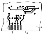
- the invention is based on one in the drawing illustrated embodiment explained in more detail. It shows the partial view of a circuit board 1, the conductor tracks 3 the contact areas 2 present at their edge area 4 end. Such contact areas can also on several edge areas be provided. When used as intended of this circuit board, it will contact these contact surfaces 2 in inserted a counter contact arrangement.
- This counter contact arrangement represents for example a female connector Connection of such circuit boards to each other also the corresponding plug connections via these contact surfaces among themselves.
- This connector between this contact surface and the counter contacts serves at the same time as the electrical connection mechanical connection. In this way, for example connection required for a retrofit Supplementary circuit board with a basic circuit board.
- circuit board edge Contact areas 2 are not formed over the entire area. Such training is extremely problematic if these contact surfaces in the process of assembling for the Printed circuit board soldering are included. Without special measures are formed on such a full area Contact area for a certain minimum width irregular tin accumulation is necessary. Through this These surfaces are irregular and too thick can no longer be properly contacted due to the counter contact.
- these contact areas are used in connection with the manufacturing process the printed circuit board these contact areas additionally structured.
- these contact areas are by a comb-like Structuring individual sub-areas formed, each merge into trace 3.
- the individual in the direction of insertion have aligned tine-shaped partial surfaces e.g. a width between 0.2 and 0.3 mm.
- the width of the recess between them is e.g. about the same size.
- this structured contact surfaces 2 included in the soldering process so a thin layer is evenly formed on the partial surfaces distributed solder layer. It results on the tine-like Partial areas a layer thickness dimension, which with regard the spring travel of the counter contacts used Poses problems.
- the PCB surface Protective layer (tinned or varnish-like protective coating) arises from the one required after the assembly of the printed circuit board Soldering process (so-called wave soldering or reflow soldering) for these individual, formed by the structuring Partial areas due to the changed surface tension conditions a flat, highly contactable Layer. In contrast to a full-surface contact area can take additional measures either before or after Soldering process are not necessary.
- Structuring of the contact surfaces 2 e.g. directly in the wave soldering process provided anyway can be soldered by wave, creating a perfect contact surface for the counter contacts.
Landscapes
- Engineering & Computer Science (AREA)
- Microelectronics & Electronic Packaging (AREA)
- Manufacturing & Machinery (AREA)
- Coupling Device And Connection With Printed Circuit (AREA)
- Chemical And Physical Treatments For Wood And The Like (AREA)
- Polysaccharides And Polysaccharide Derivatives (AREA)
- Manufacturing Of Printed Wiring (AREA)
- Electric Connection Of Electric Components To Printed Circuits (AREA)
Abstract
Description
Die Erfindung betrifft eine Leiterplatte, die an mindestens einem ihrer Randbereiche mit einer Leiterbahn verbundene Kontaktflächen aufweist. Diese dienen dazu, bei ihrem bestimmungsgemäßen Gebrauch mit jeweils einem Gegenkontakt einer Steckeranordnung zu kontaktieren. Eine Leiterplatte wird zunächst insoweit fertiggestellt, als sie entsprechend dem gewählten Leiterplatten-Layout die auf der Leiterplatte vorzusehenden Leiterbahnen und die Lötstellen in Form von Lötaugen bzw. in Form anderer mit dem Lot zu bedeckenden Flächen aufweist. Zur Bildung von Funktions- bzw. Baueinheiten werden diese Leiterplatten mit den entsprechenden Werkstücken bzw. Bauelementen bestückt. Dies erfolgt im Allgemeinen nur auf einer Seite der Leiterplatte, da die andere Seite unter anderem für das Löten der durch entsprechenden Durchtrittsöffnungen hindurchragende Anschlußstifte freigehalten wird. Eine derartige, elektrische Bauelemente tragende Leiterplatte wird z.B. als elektrische Baugruppe gegebenenfalls zusammen mit weiteren Baugruppen in eine konstruktiv entsprechend angepaßte Aufnahmeeinheit eingebracht bzw. sie wird auf eine Grundplatte aufgesteckt. Je nach Anwendungsfall werden die an mindestens einem Randbereich der Leiterplatte vorhandenen, in der Regel als Streifen von wenigen Millimetern Breite ausgebildeten eine oder mehrere Kontaktflächen unmittelbar mit einer Gegensteckeinrichtung in Eingriff gebracht. Bei der damit hergestellten elektrischen Verbindung zwischen zwei Einheiten muß eine sichere Kontaktierung erfolgen, um eine einwandfreie Funktion zu ermöglichen. Als handelsübliche Einheit können Leiterplatten bezogen werden, deren Kupferauflagen in Form von Leiterbahnen und in Form dieser Kontaktflächen entweder durch eine Vorverzinnung oder durch einen geeigneten Schutzlack gegen Korrosion geschützt sind. Durch den nach der Bestückung einer Leiterplatte mit den entsprechenden Bauelementen bzw. Werkstücken erfolgenden Lötvorgang - der beispielsweise in Form der sogenannten Schwall-Lötung oder auch in Form der sogenannten Reflow-Lötung erfolgen kann - wird das aufgebrachte Konservierungsmittel aufgebrochen und die betreffenden Stellen nehmen das Lot auf. Die genannten Kontaktflächen, die jeweils mit einem Gegenkontakt kontaktieren, werden in der Fachwelt allgemein als sogenannte Edge-Connectoren bezeichnet. Bei einem vorgenommenen Lötvorgang kommt es bei beiden genannten Leiterplattentypen ohne besondere Maßnahmen zu nicht reproduzierbaren Zinnanhäufungen. Diese führen dazu, daß eine sichere Kontaktierung nicht mehr vorausgesetzt werden kann. Es muß also, um dies zu vermeiden, eine besondere Maßnahme getroffen werden, z.B. wird bei einer als Korrosionsschutz bereits vorverzinnten Leiterplatte der die Kontaktflächen aufweisende Randbereich jeweils mit einer hitzebeständigen Abdeckung versehen. Ist das Kupfermaterial und somit auch die Kontaktflächen der Leiterplatte durch eine Lackschicht als Konservierungsmittel geschützt, so ergibt sich ebenfalls eine über diese Fläche unregelmäßig verteilte Schicht, mit einer Dickenabmessung, die eine einwandfreie Funktion der Gegenkontakte in Frage stellt.The invention relates to a circuit board that at least one of its edge regions connected to a conductor track having. These are used for their intended purpose Use with one counter contact each Contact connector arrangement. A circuit board is first to the extent that they correspond to the chosen one PCB layout to be provided on the PCB Conductor tracks and the solder joints in the form of pads or in the form of other surfaces to be covered with the solder. To form functional or structural units these circuit boards with the corresponding workpieces or Components assembled. This generally only happens on one side of the circuit board since the other side among others for soldering through through openings protruding pins is kept free. A such circuit board carrying electrical components e.g. as an electrical assembly, possibly together with other modules in a structurally adapted Recording unit introduced or it is placed on a base plate attached. Depending on the application, at least an edge region of the circuit board, in usually designed as strips a few millimeters wide one or more contact areas directly with one Mating connector brought into engagement. With that established electrical connection between two units reliable contact must be made in order to ensure flawless contact Enable function. Can as a standard unit Printed circuit boards are obtained, the copper layers of which are in the form of traces and in the form of these contact areas either by pre-tinning or by a suitable protective lacquer are protected against corrosion. By after the assembly a circuit board with the corresponding components soldering process or workpieces - for example in the form of the so-called wave soldering or also in Form of so-called reflow soldering can be done - will applied preservatives broken up and the concerned Positions take up the solder. The contact areas mentioned, who contact each other with a counter contact, are generally known in the industry as so-called edge connectors designated. When a soldering process is carried out it happens with both mentioned types of PCB without any special Measures for non-reproducible tin accumulations. These lead to the fact that a reliable contact is no longer can be assumed. So, to avoid this, a special measure is taken, e.g. is at a already pre-tinned circuit board for corrosion protection the edge areas having contact areas each with a heat-resistant cover. Is the copper material and thus also the contact surfaces of the circuit board through a Protected lacquer layer as a preservative, so results there was also an irregular distribution over this area Layer, with a thickness dimension that is a flawless Question the function of the counter contacts.
Der Lötvorgang für diese Kontaktflächen ist aber zwingend notwendig, da sonst auf Grund des Konservierungsmittels die Kontaktfähigkeit fehlt.However, the soldering process for these contact areas is mandatory necessary, otherwise the due to the preservative Contact ability is missing.
Es ist die Aufgabe der Erfindung, die für den Lötvorgang vorzunehmenden Maßnahmen zu vereinfachen, und eine optimale Kontaktfähigkeit der Kontaktflächen (Edge-Connectoren) sicherzustellen.It is the object of the invention to be carried out for the soldering process Simplify measures, and optimal contact ability of the contact areas (edge connectors).
Diese Aufgabe wird durch die im Kennzeichen des Patentanspruches angegebenen Merkmale gelöst. Das Wesentliche der Erfindung besteht darin, daß jede dieser Kontaktflächen (Edge-Connectoren) nicht mehr vollflächig ausgebildet ist, sondern in mehrere miteinander verbundenen Teilflächen strukturiert ist. Diese einzelnen Teilflächen sind hinsichtlich ihrer Abmessungen so bestimmt, daß eine hinsichtlich der sich daran ausbildenden Lotschicht mögliche maximale Dicke bei ihrem Aufbringen nicht überschritten wird. Diese Teilflächen können grundsätzlich in den unterschiedlichsten Formen realisiert sein. Sie können schräg in einem bestimmten Winkel verlaufen oder als eine Gitterstruktur mit quer und längs verlaufenden Flächenanteilen ausgebildet sein. Die miteinander verbundenen Teilflächen können in paralleler Anordnung abschnittsweise in einer sich ändernden Richtung verlaufen (Zickzack-Linienführung).This object is achieved in the characterizing part of the claim specified features solved. The essence of the invention consists in that each of these contact surfaces (edge connectors) is no longer fully formed, but structured in several interconnected partial areas is. These individual partial areas are in terms of their dimensions so determined that one with regard to it forming solder layer possible maximum thickness at their Application is not exceeded. These partial areas can basically implemented in a wide variety of forms be. They can run at an angle or as a lattice structure with transverse and longitudinal Area shares should be formed. The connected Partial areas can be arranged in sections in a parallel arrangement a changing direction (zigzag lines).
Für bestimmte Lötverfahren kann es von Vorteil sein, daß die Teilflächen durch eine kammartige Strukturierung gebildet sind. Die einzelnen Zinken sind dabei in Steckrichtung ausgerichtet. Diese Zinken sollen eine Breite von wenigen Zehntelmillimetern nicht überschreiten. Eine derartig strukturierte Kontaktfläche für diese sogenannten Edge-Connectoren erlaubt nun diese ohne irgendwelche Zusatzmaßnahmen unmittelbar in den vorzunehmenden Lötvorgang für die bestückte Leiterplatte einzubeziehen. Durch diese Strukturierung werden diese Kontaktflächen problemlos lötbar, so daß beispielsweise die Verzinnung während des üblichen Wellenlötprozesses erfolgen kann. Dies trifft sowohl auf Leiterplatten mit vorab heiß verzinnter Oberfläche, als auch für solche mit einem aufgebrachten lackartigen Konservierungsmittel zu. Ohne daß der Prozeß zusätzlich gelenkt werden muß, entstehen auf den Teilflächen gleichmäßig dünne und ebene Schichten. Ihre automatisch entstehende Schichtdicken garantieren eine einwandfreie Funktion der federnden Gegenkontakte. Bei Anwendung dieser strukturierten Lötflächen sind die Leiterplatten, deren Oberfläche mit dem lackartigen Konservierungsmittel geschützt ist, problemlos einzusetzen. Da derartige Leiterplatten preisgünstiger als Leiterplatten mit heiß verzinnter Oberfläche sind, ergibt sich dadurch auch eine entsprechende Kostenersparnis, die bei der Vielzahl der eingesetzten Leiterplatten ganz erheblich sein kann. Auf der Kontaktseite werden die mit dem Einsatz moderner Bauelemente notwendigeren kritischeren elektrischen Anforderungen voll erfüllt. Dies gilt unabhängig von der Art des vorab aufgebrachten Schutzüberzuges. Durch die Struktur der Kontaktfläche, insbesondere durch die kammartige Strukturierung, ergibt sich beim Lötvorgang eine Veränderung der Oberflächenspannung der aufgetragenen Schicht, so daß sich durch den entstehenden regelmäßigen Lotabriß kontrolliert eine gleichmäßige Lotschicht automatisch aufbaut.For certain soldering processes it can be advantageous that the Partial areas formed by a comb-like structure are. The individual tines are aligned in the direction of insertion. These tines are said to be a few tenths of a millimeter wide do not exceed. Such a structured one Contact area allowed for these so-called edge connectors now this in without any additional measures the soldering process to be carried out for the printed circuit board to involve. This structuring creates these contact areas easily solderable, so that, for example, the tinning during the usual wave soldering process can. This applies to both PCBs with hot beforehand tinned surface, as well as for those with an applied varnish-like preservatives. Without that Process must also be directed to the Subareas evenly thin and flat layers. Your automatically resulting layer thicknesses guarantee a flawless Function of the resilient counter contacts. When using of these structured soldering areas are the printed circuit boards whose Protected surface with the varnish-like preservative is easy to use. Because such circuit boards cheaper than printed circuit boards with hot-tinned Surface, this also results in a corresponding Cost savings with the large number of printed circuit boards used can be quite significant. On the contact page will become more necessary with the use of modern components more critical electrical requirements fully met. This applies regardless of the type of protective coating applied beforehand. Due to the structure of the contact surface, in particular the comb-like structure results in the soldering process a change in the surface tension of the applied Layer, so that the emerging regular Solder breakdown automatically checks an even solder layer builds up.
Im Folgenden wird die Erfindung anhand eines in der Zeichnung
dargestellten Ausführungsbeispiels näher erläutert. Es zeigt
die Teilansicht einer Leiterplatte 1, deren Leiterbahnen 3 an
dem an ihrem Randbereich 4 vorhandenen Kontaktflächen 2 enden.
Derartige Kontaktflächen können auch auf mehreren Randbereichen
vorgesehen sein. Beim bestimmungsgemäßen Gebrauch
dieser Leiterplatte wird sie mit diesen Kontaktflächen 2 in
eine Gegenkontaktanordnung eingesteckt. Diese Gegenkontaktanordnung
stellt beispielsweise eine Federleiste dar. Zur
Verbindung von derartigen Leiterplatten untereinander können
auch die entsprechenden Steckverbindungen über diese Kontaktflächen
untereinander vorgenommen werden. Diese Steckverbindung
zwischen dieser Kontaktfläche und den Gegenkontakten
dient neben der elektrischen Verbindung auch gleichzeitig zur
mechanischen Verbindung. Auf diese Weise kann auch die beispielsweise
für eine Nachrüstung erforderliche Verbindung einer
Ergänzungsleiterplatte mit einer Grundleiterplatte erfolgen.In the following, the invention is based on one in the drawing
illustrated embodiment explained in more detail. It shows
the partial view of a circuit board 1, the conductor tracks 3
the
Die im unmittelbaren Bereich des Leiterplattenrandes angeordneten
Kontaktflächen 2 sind nicht vollflächig ausgebildet.
Eine derartige Ausbildung ist dann äußerst problematisch,
wenn diese Kontaktflächen beim Prozeß des für die bestückte
Leiterplatte vorgenommenen Lötens mit einbezogen werden. Ohne
besondere Maßnahmen bilden sich an einer derartigen vollflächigen
Kontaktfläche für die eine bestimmte Mindestbreite
notwendig ist, unregelmäßige Zinnanhäufungen. Durch diesen
unregelmäßigen und zu dicken Lotauftrag sind diese Flächen
durch den Gegenkontakt nicht mehr einwandfrei kontaktierbar. The arranged in the immediate area of the circuit board
Es werden erfindungsgemäß in Verbindung mit dem Herstellungsprozeß
der Leiterplatte diese Kontaktflächen zusätzlich
strukturiert. Im Ausführungsbeispiel sind durch eine kammartige
Strukturierung einzelne Teilflächen gebildet, die jeweils
in die Leiterbahn 3 übergehen. Die einzelnen in Steckrichtung
ausgerichteten zinkenförmigen Teilflächen weisen
z.B. eine zwischen 0,2 und 0,3 mm liegende Breite auf. Die
Breite der zwischen ihnen vorhandenen Aussparung liegt z.B.
etwa in der gleichen Größenordnung. Werden nun diese derartig
strukturierten Kontaktflächen 2 in den Lötprozeß mit einbezogen,
so bildet sich an den Teilflächen eine dünne gleichmäßig
verteilte Lotschicht. Es ergibt sich dabei auf den zinkenartigen
Teilflächen eine Schichtdickenabmessung, die hinsichtlich
der Federwege der verwendeten Gegenkontakte keinerlei
Probleme aufwirft. Bei einer durchschnittlichen Dickenabmessung
von ungefähr 0,02 mm ist ausgeschlossen, daß für das Federmaterial
der Bereich der plastischen Zone erreicht wird.
In dem vorgegebenen Auslenkungsbereich kommen die notwendigen
Federkräfte zur Wirkung. Wie die Praxis zeigt, wird bei einer
derartig strukturierten Kontaktfläche eine sichere Kontaktierung
zwischen diesen Teilflächen und dem jeweiligen Gegenkontakt
erzielt. Dieser saubere und gleichmäßige Auftrag, der in
jedem Fall ohne zusätzliche Steuerung unterhalb der für eine
einwandfreie Funktion schädlichen Dickenabmessung bleibt,
wird sowohl bei einer durch einen Lacküberzug geschützten
Leiterplatte, als auch bei einer vorab heiß verzinnten Leiterplatte
erreicht. Bei der erstgenannten Leiterplatte ist im
Bereich dieser Kontaktflächen ein kontaktfähiger Schutzüberzug
in jedem Falle erforderlich. Ohne einen derartigen Überzug
wäre diese Kontaktfläche insbesondere bei mehrfach vorgenommenen
Steckversuchen aufs Äußerste korrosionsgefährdet. Es
sind also erst durch diese Maßnahme der Strukturierung solche
Leiterplatten wirtschaftlich einzusetzen. Durch Vermeidung
der vorab vorzunehmenden aufwendigen Heißverzinnung ergeben
sich Kosteneinsparungen. Außerdem ist bei Aufbringen eines
Lacküberzuges die Gefahr von Plattenverwölbungen ausgeschlossen.
Derartige Verwölbungen können bei den durch Heißverzinnung
gegen Korrosion geschützten Leiterplatten auftreten.According to the invention, they are used in connection with the manufacturing process
the printed circuit board these contact areas additionally
structured. In the exemplary embodiment are by a comb-like
Structuring individual sub-areas formed, each
merge into trace 3. The individual in the direction of insertion
have aligned tine-shaped partial surfaces
e.g. a width between 0.2 and 0.3 mm. The
The width of the recess between them is e.g.
about the same size. Now become this
Unabhängig von der für die Leiterplattenoberfläche verwendeten Schutzschicht (verzinnt bzw. lackartiger Schutzüberzug), ergibt sich bei dem nach der Bestückung der Leiterplatte notwendigen Lötvorgang (sogenannte Wellen-Lötung bzw. Reflow-Lötung) für diese einzelnen, durch die Strukturierung gebildeten Teilflächen auf Grund der geänderten Oberflächenspannungsverhältnisse eine ebene, im höchsten Maße kontaktfähige Schicht. Im Gegensatz zu einer vollflächigen Kontaktfläche können zusätzliche Maßnahmen, die entweder vor oder nach dem Lötvorgang zu treffen sind, entfallen. Durch die erfindungsgemäße Strukturierung der Kontaktflächen 2 werden diese z.B. in dem sowieso vorgesehenen Wellenlötprozeß auch unmittelbar wellenlötbar, wobei sich eine einwandfreie Kontaktierfläche für die Gegenkontakte ergibt.Regardless of the one used for the PCB surface Protective layer (tinned or varnish-like protective coating), arises from the one required after the assembly of the printed circuit board Soldering process (so-called wave soldering or reflow soldering) for these individual, formed by the structuring Partial areas due to the changed surface tension conditions a flat, highly contactable Layer. In contrast to a full-surface contact area can take additional measures either before or after Soldering process are not necessary. By the invention Structuring of the contact surfaces 2, e.g. directly in the wave soldering process provided anyway can be soldered by wave, creating a perfect contact surface for the counter contacts.
Claims (7)
dadurch gekennzeichnet,
daß zur Sicherstellung einer einwandfreien Kontaktfunktion mit dem jeweiligen Gegenkontaktelement die Kontaktfläche (2) jeweils in mehrere miteinander verbundene Teilflächen (5) strukturiert ist und daß diese Teilflächen hinsichtlich ihrer Länge- und/oder Breite derart bemessen sind, daß die in einem ungesteuerten Prozeß aufgebrachte kontaktfähige Schicht eine maximal mögliche Dickenabmessung nicht überschreitet.Printed circuit board which has at least one contact area connected to a conductor track on at least one of its edge regions, which serves to make contact with a mating contact element of a plug arrangement when used as intended and which is provided with a contactable protective layer,
characterized,
that to ensure proper contact function with the respective counter-contact element, the contact surface (2) is structured in several interconnected partial surfaces (5) and that these partial surfaces are dimensioned with respect to their length and / or width such that the contactable applied in an uncontrolled process Layer does not exceed a maximum possible thickness dimension.
dadurch gekennzeichnet,
daß die Teilflächen durch eine kammartige Strukturierung gebildet sind, deren einzelne Zinken in Steckrichtung verlaufen.Printed circuit board according to claim 1,
characterized,
that the partial surfaces are formed by a comb-like structure, the individual tines of which extend in the direction of insertion.
dadurch gekennzeichnet,
daß die Zinken der Teilfläche und die zwischen ihnen vorhandenen Zwischenräume vorzugsweise angenähert eine gleiche Breite zwischen 0,2 und 0,3 mm aufweisen.Printed circuit board according to claim 2,
characterized,
that the tines of the partial surface and the spaces between them preferably have approximately the same width between 0.2 and 0.3 mm.
dadurch gekennzeichnet,
daß die kontaktfähige Schicht auf die strukturierte Kontaktfläche unmittelbar durch denselben Lötvorgang aufgebracht ist, der die elektrische Verbindung der auf ihr aufgebrachten Bauelemente mit den Leiterbahnen bewirkt hat.Printed circuit board according to claim 1 or 2,
characterized,
that the contactable layer is applied to the structured contact surface directly by the same soldering process that has brought about the electrical connection of the components applied to it to the conductor tracks.
dadurch gekennzeichnet,
daß in den Fällen, in denen zumindest auf die strukturierte Kontaktfläche als Korrosionsschutz eine lackartige - im Zuge des nach dem Aufbringen der Bauelemente erfolgten Lötvorganges an den mit dem Lötmaterial in Kontakt tretenden Stellen aufbrechende - Schicht aufgebracht ist, nach dem Lötvorgang durch die Wirkung der Strukturierung der Kontaktfläche diese automatisch jeweils eine gleichmäßig dünne und die sichere Kontaktierungsmöglichkeit für en jeweiligen Gegenkontakt bietende Lotschicht aufweist.Printed circuit board according to claim 1 or 4,
characterized,
that in those cases in which at least a varnish-like layer is applied to the structured contact surface as corrosion protection - in the course of the soldering process which occurs after the components have been applied at the points which come into contact with the soldering material - after the soldering process by the effect of the structuring the contact surface automatically has a uniformly thin layer and the reliable contacting possibility for the respective soldering contact.
dadurch gekennzeichnet,
daß in den Fällen in denen zumindest auf die strukturierte Kontaktfläche als Korrosionsschutz eine leitende Schicht vorab aufgebracht ist, aufgrund des nach dem Aufbringen der Bauelemente erfolgten Lötvorganges durch die Wirkung der Strukturierung der Kontaktfläche, die auf ihr vorhandene ursprüngliche Schicht automatisch auf eine die sichere Kontaktierungsmöglichkeit für den jeweiligen Gegenkontakt bietende Dickenabmessung homogenisiert ist.Printed circuit board according to claim 1 or 4,
characterized,
that in cases where at least a conductive layer has been applied to the structured contact surface as corrosion protection, due to the soldering process after the application of the components by the effect of the structuring of the contact surface, the existing original layer on it automatically provides a safe contacting option for the thickness dimension offering the respective counter contact is homogenized.
dadurch gekennzeichnet,
daß die Gegenkontaktelemente die Federn einer Kontaktfederleiste darstellen.Printed circuit board according to one of the preceding claims,
characterized,
that the counter-contact elements represent the springs of a contact spring strip.
Applications Claiming Priority (2)
| Application Number | Priority Date | Filing Date | Title |
|---|---|---|---|
| DE29616339U | 1996-09-19 | ||
| DE29616339U DE29616339U1 (en) | 1996-09-19 | 1996-09-19 | Circuit board |
Publications (1)
| Publication Number | Publication Date |
|---|---|
| EP0831682A1 true EP0831682A1 (en) | 1998-03-25 |
Family
ID=8029444
Family Applications (1)
| Application Number | Title | Priority Date | Filing Date |
|---|---|---|---|
| EP97114008A Withdrawn EP0831682A1 (en) | 1996-09-19 | 1997-08-13 | Circuit board |
Country Status (6)
| Country | Link |
|---|---|
| EP (1) | EP0831682A1 (en) |
| KR (1) | KR19980024730A (en) |
| CN (1) | CN1177273A (en) |
| BR (1) | BR9704745A (en) |
| DE (1) | DE29616339U1 (en) |
| TW (1) | TW372388B (en) |
Cited By (2)
| Publication number | Priority date | Publication date | Assignee | Title |
|---|---|---|---|---|
| DE19751271A1 (en) * | 1997-11-19 | 1999-06-02 | Siemens Ag | Circuit board contact-point and edge-connector manufacturing method |
| CN104717844A (en) * | 2015-03-16 | 2015-06-17 | 珠海格力电器股份有限公司 | Wiring welding method of PCB and PCB welding structure |
Families Citing this family (3)
| Publication number | Priority date | Publication date | Assignee | Title |
|---|---|---|---|---|
| DE29616339U1 (en) * | 1996-09-19 | 1997-03-13 | Siemens AG, 80333 München | Circuit board |
| CN105543946B (en) * | 2015-12-25 | 2017-10-31 | 深圳市景旺电子股份有限公司 | A kind of method and FPC for being used to control the thick uniformity of the tin plating finger tin of FPC |
| CN113410313A (en) * | 2021-05-10 | 2021-09-17 | 深圳市百柔新材料技术有限公司 | Conductive circuit film, preparation method thereof and photovoltaic cell |
Citations (7)
| Publication number | Priority date | Publication date | Assignee | Title |
|---|---|---|---|---|
| DE2410849A1 (en) * | 1974-03-07 | 1975-09-11 | Blaupunkt Werke Gmbh | Process for soldering miniature components to boards - has blobs of solder on boards contact pads re-melted to link with component |
| DE2528000A1 (en) * | 1975-06-24 | 1977-01-20 | Licentia Gmbh | Large area solder application - involves application of solder repellant grid over silvering paste and dip or flow soldering |
| DE9202633U1 (en) * | 1992-02-28 | 1992-05-27 | Siemens AG, 8000 München | Copper-clad circuit board with ground contact areas |
| JPH05136551A (en) * | 1991-11-08 | 1993-06-01 | Furukawa Electric Co Ltd:The | Solder coat printed circuit board |
| JPH06188533A (en) * | 1992-12-16 | 1994-07-08 | Fujitsu Ltd | Printed wiring board |
| JPH0831478A (en) * | 1994-07-19 | 1996-02-02 | Sony Corp | Electrode connection device |
| DE29616339U1 (en) * | 1996-09-19 | 1997-03-13 | Siemens AG, 80333 München | Circuit board |
-
1996
- 1996-09-19 DE DE29616339U patent/DE29616339U1/en not_active Expired - Lifetime
-
1997
- 1997-08-13 EP EP97114008A patent/EP0831682A1/en not_active Withdrawn
- 1997-08-26 TW TW086112240A patent/TW372388B/en active
- 1997-09-19 KR KR1019970047641A patent/KR19980024730A/en not_active Withdrawn
- 1997-09-19 CN CN97119309A patent/CN1177273A/en active Pending
- 1997-09-19 BR BR9704745A patent/BR9704745A/en not_active IP Right Cessation
Patent Citations (7)
| Publication number | Priority date | Publication date | Assignee | Title |
|---|---|---|---|---|
| DE2410849A1 (en) * | 1974-03-07 | 1975-09-11 | Blaupunkt Werke Gmbh | Process for soldering miniature components to boards - has blobs of solder on boards contact pads re-melted to link with component |
| DE2528000A1 (en) * | 1975-06-24 | 1977-01-20 | Licentia Gmbh | Large area solder application - involves application of solder repellant grid over silvering paste and dip or flow soldering |
| JPH05136551A (en) * | 1991-11-08 | 1993-06-01 | Furukawa Electric Co Ltd:The | Solder coat printed circuit board |
| DE9202633U1 (en) * | 1992-02-28 | 1992-05-27 | Siemens AG, 8000 München | Copper-clad circuit board with ground contact areas |
| JPH06188533A (en) * | 1992-12-16 | 1994-07-08 | Fujitsu Ltd | Printed wiring board |
| JPH0831478A (en) * | 1994-07-19 | 1996-02-02 | Sony Corp | Electrode connection device |
| DE29616339U1 (en) * | 1996-09-19 | 1997-03-13 | Siemens AG, 80333 München | Circuit board |
Non-Patent Citations (4)
| Title |
|---|
| "Dust collector for PC I/O tab", IBM TECHNICAL DISCLOSURE BULLETIN., vol. 30, no. 8, January 1988 (1988-01-01), NEW YORK US, pages 352 - 353, XP002041986 * |
| PATENT ABSTRACTS OF JAPAN vol. 17, no. 518 (E - 1434) 17 September 1993 (1993-09-17) * |
| PATENT ABSTRACTS OF JAPAN vol. 18, no. 531 (E - 1614) 7 October 1994 (1994-10-07) * |
| PATENT ABSTRACTS OF JAPAN vol. 96, no. 6 28 June 1996 (1996-06-28) * |
Cited By (3)
| Publication number | Priority date | Publication date | Assignee | Title |
|---|---|---|---|---|
| DE19751271A1 (en) * | 1997-11-19 | 1999-06-02 | Siemens Ag | Circuit board contact-point and edge-connector manufacturing method |
| DE19751271B4 (en) * | 1997-11-19 | 2006-07-06 | Siemens Ag | Method for producing peripheral contact surfaces on printed circuit boards |
| CN104717844A (en) * | 2015-03-16 | 2015-06-17 | 珠海格力电器股份有限公司 | Wiring welding method of PCB and PCB welding structure |
Also Published As
| Publication number | Publication date |
|---|---|
| CN1177273A (en) | 1998-03-25 |
| DE29616339U1 (en) | 1997-03-13 |
| BR9704745A (en) | 1998-11-10 |
| KR19980024730A (en) | 1998-07-06 |
| TW372388B (en) | 1999-10-21 |
Similar Documents
| Publication | Publication Date | Title |
|---|---|---|
| DE69302296T2 (en) | Circuit board | |
| DE4203605A1 (en) | ELECTRIC CONNECTOR | |
| DE19809138A1 (en) | Printed circuit board with SMD components | |
| DE4192038C2 (en) | PCB assembly mfr. permitting wave soldering | |
| DE102017105680A1 (en) | Surface mounted resistor | |
| DE4425803A1 (en) | Printed circuit board | |
| DE60128537T2 (en) | ASSEMBLY TO CONNECT AT LEAST TWO PRINTED CIRCUITS | |
| DE102004041173B4 (en) | Soldering between a strip of bus bar and a printed substrate | |
| DE4303743A1 (en) | ||
| DE3710394C2 (en) | ||
| DE112017006956B4 (en) | Method of manufacturing a power semiconductor device and power semiconductor device | |
| DE4407092A1 (en) | Printed circuit board for surface-mounted electrical components | |
| DE112015003374B4 (en) | circuit arrangement | |
| EP0831682A1 (en) | Circuit board | |
| EP0238823B1 (en) | Multiple plug for a connector with contact springs arranged in at least two parallel rows | |
| EP0680117A2 (en) | Plug connection between backplane and printed circuits | |
| DE3731413A1 (en) | Electrical switching apparatus | |
| DE102005039198A1 (en) | A method of arranging a terminal on a printed card, and a terminal-mounted printed card and electrical connector housing for receiving the printed card with the terminal disposed thereon, both made by the method | |
| DE19805492C2 (en) | Circuit board | |
| DE10301227A1 (en) | Forming conductor ends of a ribbon cable | |
| DE102015115819A1 (en) | Conductor bridge element and mounting belt and circuit boards with such | |
| DE2232794B1 (en) | Plate-shaped electronic component | |
| DE10318589A1 (en) | Printed circuit board assembly | |
| DE19802089C2 (en) | Contact plug connection and contact plug | |
| EP0508395B1 (en) | Grounding device |
Legal Events
| Date | Code | Title | Description |
|---|---|---|---|
| PUAI | Public reference made under article 153(3) epc to a published international application that has entered the european phase |
Free format text: ORIGINAL CODE: 0009012 |
|
| AK | Designated contracting states |
Kind code of ref document: A1 Designated state(s): AT BE CH DE ES GB IE IT LI NL |
|
| AX | Request for extension of the european patent |
Free format text: AL;LT;LV;RO;SI |
|
| 17P | Request for examination filed |
Effective date: 19980917 |
|
| AKX | Designation fees paid |
Free format text: AT BE CH DE ES GB IE IT LI NL |
|
| RBV | Designated contracting states (corrected) |
Designated state(s): AT BE CH DE ES GB IE IT LI NL |
|
| STAA | Information on the status of an ep patent application or granted ep patent |
Free format text: STATUS: THE APPLICATION IS DEEMED TO BE WITHDRAWN |
|
| 18D | Application deemed to be withdrawn |
Effective date: 20010301 |