EP0582444A1 - Ultrareines Siliziumkarbid und daraus hergestellte Hochtemperaturbearbeitungseinrichtung für Halbleiter - Google Patents
Ultrareines Siliziumkarbid und daraus hergestellte Hochtemperaturbearbeitungseinrichtung für Halbleiter Download PDFInfo
- Publication number
- EP0582444A1 EP0582444A1 EP93306021A EP93306021A EP0582444A1 EP 0582444 A1 EP0582444 A1 EP 0582444A1 EP 93306021 A EP93306021 A EP 93306021A EP 93306021 A EP93306021 A EP 93306021A EP 0582444 A1 EP0582444 A1 EP 0582444A1
- Authority
- EP
- European Patent Office
- Prior art keywords
- sic
- cvd
- deposition chamber
- furnace
- deposition
- Prior art date
- Legal status (The legal status is an assumption and is not a legal conclusion. Google has not performed a legal analysis and makes no representation as to the accuracy of the status listed.)
- Withdrawn
Links
- 239000004065 semiconductor Substances 0.000 title claims abstract description 36
- 238000012545 processing Methods 0.000 title claims abstract description 25
- 229910010271 silicon carbide Inorganic materials 0.000 title description 84
- HBMJWWWQQXIZIP-UHFFFAOYSA-N silicon carbide Chemical compound [Si+]#[C-] HBMJWWWQQXIZIP-UHFFFAOYSA-N 0.000 title description 46
- 230000008021 deposition Effects 0.000 claims abstract description 61
- 238000000034 method Methods 0.000 claims abstract description 39
- 230000008569 process Effects 0.000 claims abstract description 29
- 239000012535 impurity Substances 0.000 claims abstract description 23
- 238000001036 glow-discharge mass spectrometry Methods 0.000 claims abstract description 9
- 229910052782 aluminium Inorganic materials 0.000 claims abstract description 3
- 229910052787 antimony Inorganic materials 0.000 claims abstract description 3
- 229910052785 arsenic Inorganic materials 0.000 claims abstract description 3
- 229910052796 boron Inorganic materials 0.000 claims abstract description 3
- 229910052793 cadmium Inorganic materials 0.000 claims abstract description 3
- 229910052791 calcium Inorganic materials 0.000 claims abstract description 3
- 229910052804 chromium Inorganic materials 0.000 claims abstract description 3
- 229910052802 copper Inorganic materials 0.000 claims abstract description 3
- 229910052742 iron Inorganic materials 0.000 claims abstract description 3
- 229910052744 lithium Inorganic materials 0.000 claims abstract description 3
- 229910052749 magnesium Inorganic materials 0.000 claims abstract description 3
- 229910052748 manganese Inorganic materials 0.000 claims abstract description 3
- 229910052698 phosphorus Inorganic materials 0.000 claims abstract description 3
- 229910052700 potassium Inorganic materials 0.000 claims abstract description 3
- 229910052719 titanium Inorganic materials 0.000 claims abstract description 3
- 229910052726 zirconium Inorganic materials 0.000 claims abstract 2
- 239000007789 gas Substances 0.000 claims description 30
- 239000001257 hydrogen Substances 0.000 claims description 12
- 229910052739 hydrogen Inorganic materials 0.000 claims description 12
- 239000011236 particulate material Substances 0.000 claims description 8
- 239000000919 ceramic Substances 0.000 claims description 5
- 238000009413 insulation Methods 0.000 claims description 4
- 239000005055 methyl trichlorosilane Substances 0.000 claims description 4
- JLUFWMXJHAVVNN-UHFFFAOYSA-N methyltrichlorosilane Chemical compound C[Si](Cl)(Cl)Cl JLUFWMXJHAVVNN-UHFFFAOYSA-N 0.000 claims description 4
- 239000000126 substance Substances 0.000 claims description 4
- 230000001681 protective effect Effects 0.000 claims description 2
- 125000004435 hydrogen atom Chemical class [H]* 0.000 claims 1
- 235000012431 wafers Nutrition 0.000 abstract description 64
- 238000000151 deposition Methods 0.000 abstract description 54
- 238000005229 chemical vapour deposition Methods 0.000 abstract description 16
- 238000005137 deposition process Methods 0.000 abstract 1
- 239000013618 particulate matter Substances 0.000 abstract 1
- 239000000463 material Substances 0.000 description 19
- OKTJSMMVPCPJKN-UHFFFAOYSA-N Carbon Chemical compound [C] OKTJSMMVPCPJKN-UHFFFAOYSA-N 0.000 description 18
- UFHFLCQGNIYNRP-UHFFFAOYSA-N Hydrogen Chemical compound [H][H] UFHFLCQGNIYNRP-UHFFFAOYSA-N 0.000 description 17
- VYPSYNLAJGMNEJ-UHFFFAOYSA-N silicon dioxide Inorganic materials O=[Si]=O VYPSYNLAJGMNEJ-UHFFFAOYSA-N 0.000 description 15
- 239000010453 quartz Substances 0.000 description 13
- QVGXLLKOCUKJST-UHFFFAOYSA-N atomic oxygen Chemical compound [O] QVGXLLKOCUKJST-UHFFFAOYSA-N 0.000 description 12
- 239000001301 oxygen Substances 0.000 description 12
- 229910052760 oxygen Inorganic materials 0.000 description 12
- 229910052799 carbon Inorganic materials 0.000 description 10
- 238000009792 diffusion process Methods 0.000 description 9
- 239000010439 graphite Substances 0.000 description 9
- 229910002804 graphite Inorganic materials 0.000 description 9
- XKRFYHLGVUSROY-UHFFFAOYSA-N Argon Chemical compound [Ar] XKRFYHLGVUSROY-UHFFFAOYSA-N 0.000 description 8
- 238000013461 design Methods 0.000 description 8
- 239000000356 contaminant Substances 0.000 description 6
- 238000004519 manufacturing process Methods 0.000 description 6
- 229910052710 silicon Inorganic materials 0.000 description 6
- XUIMIQQOPSSXEZ-UHFFFAOYSA-N Silicon Chemical compound [Si] XUIMIQQOPSSXEZ-UHFFFAOYSA-N 0.000 description 5
- 238000000576 coating method Methods 0.000 description 5
- 229910003465 moissanite Inorganic materials 0.000 description 5
- 239000000047 product Substances 0.000 description 5
- 239000010703 silicon Substances 0.000 description 5
- 239000000758 substrate Substances 0.000 description 5
- 238000012360 testing method Methods 0.000 description 5
- 229920000049 Carbon (fiber) Polymers 0.000 description 4
- 229910052786 argon Inorganic materials 0.000 description 4
- 239000004917 carbon fiber Substances 0.000 description 4
- 239000011248 coating agent Substances 0.000 description 4
- 238000010438 heat treatment Methods 0.000 description 4
- 238000005259 measurement Methods 0.000 description 4
- 229910052751 metal Inorganic materials 0.000 description 4
- 239000002184 metal Substances 0.000 description 4
- PXHVJJICTQNCMI-UHFFFAOYSA-N Nickel Chemical compound [Ni] PXHVJJICTQNCMI-UHFFFAOYSA-N 0.000 description 3
- 230000004888 barrier function Effects 0.000 description 3
- 230000008859 change Effects 0.000 description 3
- 239000002131 composite material Substances 0.000 description 3
- 238000001816 cooling Methods 0.000 description 3
- 230000008878 coupling Effects 0.000 description 3
- 238000010168 coupling process Methods 0.000 description 3
- 238000005859 coupling reaction Methods 0.000 description 3
- 239000000945 filler Substances 0.000 description 3
- 239000000203 mixture Substances 0.000 description 3
- 238000012544 monitoring process Methods 0.000 description 3
- TWNQGVIAIRXVLR-UHFFFAOYSA-N oxo(oxoalumanyloxy)alumane Chemical compound O=[Al]O[Al]=O TWNQGVIAIRXVLR-UHFFFAOYSA-N 0.000 description 3
- XLYOFNOQVPJJNP-UHFFFAOYSA-N water Substances O XLYOFNOQVPJJNP-UHFFFAOYSA-N 0.000 description 3
- QGZKDVFQNNGYKY-UHFFFAOYSA-N Ammonia Chemical compound N QGZKDVFQNNGYKY-UHFFFAOYSA-N 0.000 description 2
- IJGRMHOSHXDMSA-UHFFFAOYSA-N Atomic nitrogen Chemical compound N#N IJGRMHOSHXDMSA-UHFFFAOYSA-N 0.000 description 2
- CURLTUGMZLYLDI-UHFFFAOYSA-N Carbon dioxide Chemical compound O=C=O CURLTUGMZLYLDI-UHFFFAOYSA-N 0.000 description 2
- XEEYBQQBJWHFJM-UHFFFAOYSA-N Iron Chemical compound [Fe] XEEYBQQBJWHFJM-UHFFFAOYSA-N 0.000 description 2
- 230000002411 adverse Effects 0.000 description 2
- 230000000903 blocking effect Effects 0.000 description 2
- 239000011575 calcium Substances 0.000 description 2
- 239000012159 carrier gas Substances 0.000 description 2
- 230000003197 catalytic effect Effects 0.000 description 2
- 238000006243 chemical reaction Methods 0.000 description 2
- 239000000460 chlorine Substances 0.000 description 2
- 239000011651 chromium Substances 0.000 description 2
- 238000004891 communication Methods 0.000 description 2
- 239000002826 coolant Substances 0.000 description 2
- 239000010949 copper Substances 0.000 description 2
- 230000001627 detrimental effect Effects 0.000 description 2
- -1 e.g. Substances 0.000 description 2
- 238000001704 evaporation Methods 0.000 description 2
- 230000008020 evaporation Effects 0.000 description 2
- 239000010408 film Substances 0.000 description 2
- 238000002955 isolation Methods 0.000 description 2
- 239000011777 magnesium Substances 0.000 description 2
- 239000011572 manganese Substances 0.000 description 2
- 229910052752 metalloid Inorganic materials 0.000 description 2
- 150000002738 metalloids Chemical class 0.000 description 2
- 150000002739 metals Chemical class 0.000 description 2
- 229910052755 nonmetal Inorganic materials 0.000 description 2
- 230000003287 optical effect Effects 0.000 description 2
- 235000012771 pancakes Nutrition 0.000 description 2
- 238000005240 physical vapour deposition Methods 0.000 description 2
- 230000035939 shock Effects 0.000 description 2
- 239000011734 sodium Substances 0.000 description 2
- 239000010409 thin film Substances 0.000 description 2
- 239000010936 titanium Substances 0.000 description 2
- ZOXJGFHDIHLPTG-UHFFFAOYSA-N Boron Chemical compound [B] ZOXJGFHDIHLPTG-UHFFFAOYSA-N 0.000 description 1
- OYPRJOBELJOOCE-UHFFFAOYSA-N Calcium Chemical compound [Ca] OYPRJOBELJOOCE-UHFFFAOYSA-N 0.000 description 1
- ZAMOUSCENKQFHK-UHFFFAOYSA-N Chlorine atom Chemical compound [Cl] ZAMOUSCENKQFHK-UHFFFAOYSA-N 0.000 description 1
- VYZAMTAEIAYCRO-UHFFFAOYSA-N Chromium Chemical compound [Cr] VYZAMTAEIAYCRO-UHFFFAOYSA-N 0.000 description 1
- RYGMFSIKBFXOCR-UHFFFAOYSA-N Copper Chemical compound [Cu] RYGMFSIKBFXOCR-UHFFFAOYSA-N 0.000 description 1
- DGAQECJNVWCQMB-PUAWFVPOSA-M Ilexoside XXIX Chemical compound C[C@@H]1CC[C@@]2(CC[C@@]3(C(=CC[C@H]4[C@]3(CC[C@@H]5[C@@]4(CC[C@@H](C5(C)C)OS(=O)(=O)[O-])C)C)[C@@H]2[C@]1(C)O)C)C(=O)O[C@H]6[C@@H]([C@H]([C@@H]([C@H](O6)CO)O)O)O.[Na+] DGAQECJNVWCQMB-PUAWFVPOSA-M 0.000 description 1
- WHXSMMKQMYFTQS-UHFFFAOYSA-N Lithium Chemical compound [Li] WHXSMMKQMYFTQS-UHFFFAOYSA-N 0.000 description 1
- FYYHWMGAXLPEAU-UHFFFAOYSA-N Magnesium Chemical compound [Mg] FYYHWMGAXLPEAU-UHFFFAOYSA-N 0.000 description 1
- PWHULOQIROXLJO-UHFFFAOYSA-N Manganese Chemical compound [Mn] PWHULOQIROXLJO-UHFFFAOYSA-N 0.000 description 1
- GRYLNZFGIOXLOG-UHFFFAOYSA-N Nitric acid Chemical compound O[N+]([O-])=O GRYLNZFGIOXLOG-UHFFFAOYSA-N 0.000 description 1
- OAICVXFJPJFONN-UHFFFAOYSA-N Phosphorus Chemical compound [P] OAICVXFJPJFONN-UHFFFAOYSA-N 0.000 description 1
- ZLMJMSJWJFRBEC-UHFFFAOYSA-N Potassium Chemical compound [K] ZLMJMSJWJFRBEC-UHFFFAOYSA-N 0.000 description 1
- RTAQQCXQSZGOHL-UHFFFAOYSA-N Titanium Chemical compound [Ti] RTAQQCXQSZGOHL-UHFFFAOYSA-N 0.000 description 1
- 229910052783 alkali metal Inorganic materials 0.000 description 1
- 150000001340 alkali metals Chemical class 0.000 description 1
- XAGFODPZIPBFFR-UHFFFAOYSA-N aluminium Chemical compound [Al] XAGFODPZIPBFFR-UHFFFAOYSA-N 0.000 description 1
- 229910021529 ammonia Inorganic materials 0.000 description 1
- WATWJIUSRGPENY-UHFFFAOYSA-N antimony atom Chemical compound [Sb] WATWJIUSRGPENY-UHFFFAOYSA-N 0.000 description 1
- 238000013459 approach Methods 0.000 description 1
- RQNWIZPPADIBDY-UHFFFAOYSA-N arsenic atom Chemical compound [As] RQNWIZPPADIBDY-UHFFFAOYSA-N 0.000 description 1
- 238000009529 body temperature measurement Methods 0.000 description 1
- 239000006227 byproduct Substances 0.000 description 1
- BDOSMKKIYDKNTQ-UHFFFAOYSA-N cadmium atom Chemical compound [Cd] BDOSMKKIYDKNTQ-UHFFFAOYSA-N 0.000 description 1
- 229910002092 carbon dioxide Inorganic materials 0.000 description 1
- 239000001569 carbon dioxide Substances 0.000 description 1
- 238000005266 casting Methods 0.000 description 1
- 239000007795 chemical reaction product Substances 0.000 description 1
- 229910052801 chlorine Inorganic materials 0.000 description 1
- 238000004140 cleaning Methods 0.000 description 1
- 230000003749 cleanliness Effects 0.000 description 1
- 230000000052 comparative effect Effects 0.000 description 1
- 150000001875 compounds Chemical class 0.000 description 1
- 238000009833 condensation Methods 0.000 description 1
- 230000005494 condensation Effects 0.000 description 1
- 238000011109 contamination Methods 0.000 description 1
- 230000008602 contraction Effects 0.000 description 1
- 239000013078 crystal Substances 0.000 description 1
- 230000007423 decrease Effects 0.000 description 1
- 230000001419 dependent effect Effects 0.000 description 1
- 229910003460 diamond Inorganic materials 0.000 description 1
- 239000010432 diamond Substances 0.000 description 1
- 239000003085 diluting agent Substances 0.000 description 1
- 239000002657 fibrous material Substances 0.000 description 1
- 238000009501 film coating Methods 0.000 description 1
- 239000005350 fused silica glass Substances 0.000 description 1
- 238000010574 gas phase reaction Methods 0.000 description 1
- 239000008246 gaseous mixture Substances 0.000 description 1
- 238000005247 gettering Methods 0.000 description 1
- 229910052734 helium Inorganic materials 0.000 description 1
- 239000001307 helium Substances 0.000 description 1
- SWQJXJOGLNCZEY-UHFFFAOYSA-N helium atom Chemical compound [He] SWQJXJOGLNCZEY-UHFFFAOYSA-N 0.000 description 1
- 239000011261 inert gas Substances 0.000 description 1
- 238000002347 injection Methods 0.000 description 1
- 239000007924 injection Substances 0.000 description 1
- 239000011810 insulating material Substances 0.000 description 1
- 239000007788 liquid Substances 0.000 description 1
- 238000003754 machining Methods 0.000 description 1
- VNWKTOKETHGBQD-UHFFFAOYSA-N methane Chemical compound C VNWKTOKETHGBQD-UHFFFAOYSA-N 0.000 description 1
- 239000002808 molecular sieve Substances 0.000 description 1
- QPJSUIGXIBEQAC-UHFFFAOYSA-N n-(2,4-dichloro-5-propan-2-yloxyphenyl)acetamide Chemical compound CC(C)OC1=CC(NC(C)=O)=C(Cl)C=C1Cl QPJSUIGXIBEQAC-UHFFFAOYSA-N 0.000 description 1
- 229910052759 nickel Inorganic materials 0.000 description 1
- 229910017604 nitric acid Inorganic materials 0.000 description 1
- 229910052757 nitrogen Inorganic materials 0.000 description 1
- 238000010943 off-gassing Methods 0.000 description 1
- 230000003647 oxidation Effects 0.000 description 1
- 238000007254 oxidation reaction Methods 0.000 description 1
- 239000002245 particle Substances 0.000 description 1
- 239000011574 phosphorus Substances 0.000 description 1
- 238000005498 polishing Methods 0.000 description 1
- 239000011591 potassium Substances 0.000 description 1
- 230000009467 reduction Effects 0.000 description 1
- 238000011160 research Methods 0.000 description 1
- 238000007789 sealing Methods 0.000 description 1
- VSZWPYCFIRKVQL-UHFFFAOYSA-N selanylidenegallium;selenium Chemical compound [Se].[Se]=[Ga].[Se]=[Ga] VSZWPYCFIRKVQL-UHFFFAOYSA-N 0.000 description 1
- 238000005389 semiconductor device fabrication Methods 0.000 description 1
- 238000000926 separation method Methods 0.000 description 1
- 229910052708 sodium Inorganic materials 0.000 description 1
- URGAHOPLAPQHLN-UHFFFAOYSA-N sodium aluminosilicate Chemical compound [Na+].[Al+3].[O-][Si]([O-])=O.[O-][Si]([O-])=O URGAHOPLAPQHLN-UHFFFAOYSA-N 0.000 description 1
- 239000000243 solution Substances 0.000 description 1
- 238000005477 sputtering target Methods 0.000 description 1
- 229910001220 stainless steel Inorganic materials 0.000 description 1
- 239000010935 stainless steel Substances 0.000 description 1
- 238000010561 standard procedure Methods 0.000 description 1
- 238000006467 substitution reaction Methods 0.000 description 1
- 239000011573 trace mineral Substances 0.000 description 1
- 235000013619 trace mineral Nutrition 0.000 description 1
Images



Classifications
-
- C—CHEMISTRY; METALLURGY
- C04—CEMENTS; CONCRETE; ARTIFICIAL STONE; CERAMICS; REFRACTORIES
- C04B—LIME, MAGNESIA; SLAG; CEMENTS; COMPOSITIONS THEREOF, e.g. MORTARS, CONCRETE OR LIKE BUILDING MATERIALS; ARTIFICIAL STONE; CERAMICS; REFRACTORIES; TREATMENT OF NATURAL STONE
- C04B35/00—Shaped ceramic products characterised by their composition; Ceramics compositions; Processing powders of inorganic compounds preparatory to the manufacturing of ceramic products
- C04B35/515—Shaped ceramic products characterised by their composition; Ceramics compositions; Processing powders of inorganic compounds preparatory to the manufacturing of ceramic products based on non-oxide ceramics
- C04B35/56—Shaped ceramic products characterised by their composition; Ceramics compositions; Processing powders of inorganic compounds preparatory to the manufacturing of ceramic products based on non-oxide ceramics based on carbides or oxycarbides
- C04B35/565—Shaped ceramic products characterised by their composition; Ceramics compositions; Processing powders of inorganic compounds preparatory to the manufacturing of ceramic products based on non-oxide ceramics based on carbides or oxycarbides based on silicon carbide
- C04B35/571—Shaped ceramic products characterised by their composition; Ceramics compositions; Processing powders of inorganic compounds preparatory to the manufacturing of ceramic products based on non-oxide ceramics based on carbides or oxycarbides based on silicon carbide obtained from Si-containing polymer precursors or organosilicon monomers
-
- C—CHEMISTRY; METALLURGY
- C23—COATING METALLIC MATERIAL; COATING MATERIAL WITH METALLIC MATERIAL; CHEMICAL SURFACE TREATMENT; DIFFUSION TREATMENT OF METALLIC MATERIAL; COATING BY VACUUM EVAPORATION, BY SPUTTERING, BY ION IMPLANTATION OR BY CHEMICAL VAPOUR DEPOSITION, IN GENERAL; INHIBITING CORROSION OF METALLIC MATERIAL OR INCRUSTATION IN GENERAL
- C23C—COATING METALLIC MATERIAL; COATING MATERIAL WITH METALLIC MATERIAL; SURFACE TREATMENT OF METALLIC MATERIAL BY DIFFUSION INTO THE SURFACE, BY CHEMICAL CONVERSION OR SUBSTITUTION; COATING BY VACUUM EVAPORATION, BY SPUTTERING, BY ION IMPLANTATION OR BY CHEMICAL VAPOUR DEPOSITION, IN GENERAL
- C23C16/00—Chemical coating by decomposition of gaseous compounds, without leaving reaction products of surface material in the coating, i.e. chemical vapour deposition [CVD] processes
- C23C16/01—Chemical coating by decomposition of gaseous compounds, without leaving reaction products of surface material in the coating, i.e. chemical vapour deposition [CVD] processes on temporary substrates, e.g. substrates subsequently removed by etching
-
- C—CHEMISTRY; METALLURGY
- C23—COATING METALLIC MATERIAL; COATING MATERIAL WITH METALLIC MATERIAL; CHEMICAL SURFACE TREATMENT; DIFFUSION TREATMENT OF METALLIC MATERIAL; COATING BY VACUUM EVAPORATION, BY SPUTTERING, BY ION IMPLANTATION OR BY CHEMICAL VAPOUR DEPOSITION, IN GENERAL; INHIBITING CORROSION OF METALLIC MATERIAL OR INCRUSTATION IN GENERAL
- C23C—COATING METALLIC MATERIAL; COATING MATERIAL WITH METALLIC MATERIAL; SURFACE TREATMENT OF METALLIC MATERIAL BY DIFFUSION INTO THE SURFACE, BY CHEMICAL CONVERSION OR SUBSTITUTION; COATING BY VACUUM EVAPORATION, BY SPUTTERING, BY ION IMPLANTATION OR BY CHEMICAL VAPOUR DEPOSITION, IN GENERAL
- C23C16/00—Chemical coating by decomposition of gaseous compounds, without leaving reaction products of surface material in the coating, i.e. chemical vapour deposition [CVD] processes
- C23C16/22—Chemical coating by decomposition of gaseous compounds, without leaving reaction products of surface material in the coating, i.e. chemical vapour deposition [CVD] processes characterised by the deposition of inorganic material, other than metallic material
- C23C16/30—Deposition of compounds, mixtures or solid solutions, e.g. borides, carbides, nitrides
- C23C16/32—Carbides
- C23C16/325—Silicon carbide
-
- C—CHEMISTRY; METALLURGY
- C23—COATING METALLIC MATERIAL; COATING MATERIAL WITH METALLIC MATERIAL; CHEMICAL SURFACE TREATMENT; DIFFUSION TREATMENT OF METALLIC MATERIAL; COATING BY VACUUM EVAPORATION, BY SPUTTERING, BY ION IMPLANTATION OR BY CHEMICAL VAPOUR DEPOSITION, IN GENERAL; INHIBITING CORROSION OF METALLIC MATERIAL OR INCRUSTATION IN GENERAL
- C23C—COATING METALLIC MATERIAL; COATING MATERIAL WITH METALLIC MATERIAL; SURFACE TREATMENT OF METALLIC MATERIAL BY DIFFUSION INTO THE SURFACE, BY CHEMICAL CONVERSION OR SUBSTITUTION; COATING BY VACUUM EVAPORATION, BY SPUTTERING, BY ION IMPLANTATION OR BY CHEMICAL VAPOUR DEPOSITION, IN GENERAL
- C23C16/00—Chemical coating by decomposition of gaseous compounds, without leaving reaction products of surface material in the coating, i.e. chemical vapour deposition [CVD] processes
- C23C16/44—Chemical coating by decomposition of gaseous compounds, without leaving reaction products of surface material in the coating, i.e. chemical vapour deposition [CVD] processes characterised by the method of coating
- C23C16/4401—Means for minimising impurities, e.g. dust, moisture or residual gas, in the reaction chamber
- C23C16/4404—Coatings or surface treatment on the inside of the reaction chamber or on parts thereof
Definitions
- the present invention is directed to ultra or very high purity, monolithic, free-standing silicon carbide which is produced by chemical vapor deposition under very carefully controlled conditions, and applications of such CVD-SiC for various high temperature semiconductor processing equipment, particularly furnace furniture (e.g. wafer boats, process tubes, cantilever paddles or rods, and dummy wafers) and wafer handling equipment (e.g. susceptors, vacuum chucks and transport rings).
- furnace furniture e.g. wafer boats, process tubes, cantilever paddles or rods, and dummy wafers
- wafer handling equipment e.g. susceptors, vacuum chucks and transport rings.
- Various structural supports and equipment for handling wafers are required during treatment at elevated temperatures to manufacture such semiconductor devices as diodes, transistors and integrated circuits.
- the wafers are typically heated to elevated temperatures up to about 1350°C.
- the stock material of choice from which to fabricate various semiconductor processing furnace furniture and wafer handling equipment would possess excellent thermal shock resistance, high mechanical strength, the ability to retain its shape through a large number of heating and cooling cycles (thermal stability) and the material must not outgas, i.e. release impurities (dust-like particles) during loading, processing and unloading of the wafers in the furnace.
- 5A-5C schematic typically have (1) a furnace liner which is made of quartz, reaction-bonded (RB) or reaction-sintered SiC with a thin CVD-SiC coating, or graphite coated with CVD-SiC, (2) a process tube made of quartz or RB-SiC coated with CVD-SiC, (3) wafer boats made of quartz, RB-SiC coated with CVD-SiC or graphite coated with CVD-SiC and (4) a cantilever system onto which the boats are mounted and inserted into the furnace.
- the cantilever system uses either a paddle or rods onto which the boats "sit" during loading, processing and unloading. See, for example, U.S. Pat. No. 4,516,897.
- the paddles and rods are typically made of quartz or RB-SiC coated with CVD-SiC.
- the wafer boat may be fully loaded with the Si wafers to be treated. However, should any wafer slots in the boats be unfilled or should various monitoring or test functions be required, then dummy (false or imitation) wafers may be used as fillers or product wafer substitutes. Such dummy wafers are usually made of high purity material, such as quartz or SiC.
- Susceptor plates are typically made of graphite coated with CVD-SiC.
- Vacuum chucks (see Fig. 7 schematic) and, in particular, the suction heads thereof are usually made of stainless steel and other metals, as well as such ceramics as aluminum oxide (Al2O3) and SiC.
- Such suction heads are usually perforated to allow a vacuum to be established across their faces. See, for example, U.S. Pat. No. 4,906,011.
- Transport rings see Fig.
- quartz and such ceramics as Al2O3 and SiC are currently made of quartz and such ceramics as Al2O3 and SiC.
- Such wafer handling equipment is often made of quartz glass (fused silica) because of its high purity, relatively low cost and ease of fabrication into the desired shapes.
- the quartz components lose their mechanical strength and devitrify with time at the high processing temperatures involved.
- the quartz components are susceptible to extreme distortion (change in shape or dimensions) from frequent heating and cooling of the material during the wafer processing involved, and the quartz also does not stand up well to the frequent cleaning with such solutions as hydrofluoric/nitric acid required to maintain the ultra pure furnace environment desired. Because of these shortcomings, such alternative materials as SiC have been developed.
- SiC has been shown to be an excellent choice, especially for semiconductor processing furnace furniture. See, for example, U.S. Pat. Nos. 4,761,134; 4,998,879 and 4,999,228.
- Such known composite furniture components consist of RB-SiC coated with CVD-SiC or graphite coated with CVD-SiC. Both the RB-SiC and graphite substrates are highly impure, containing numerous contaminants detrimental to quality semiconductor device fabrication. To help overcome this problem the substrates are coated with a thin layer of CVD-SiC which provides a diffusion barrier to prevent contaminants in the substrate material (RB-SiC or graphite) from outgassing in the semiconductor processing furnace.
- SiC methyltrichlosilane
- H2 hydrogen
- inert or non-reactive gas such as argon, helium or nitrogen, argon being preferred.
- Monolithic, free-standing SiC is typically made by providing a furnace having a deposition chamber and a removable mandrel (e.g. graphite) therein, and pyrolytically depositing SiC from the gaseous mixture on the removable mandrel.
- MTS provides both Si and C in stoichiometric (1:1) ratios.
- the inert or non-reactive gas acts as a carrier gas for MTS (which is liquid at ambient temperatures); can be varied to adjust the gas flow velocity through the furnace as is necessary to sweep reaction products, such as HCl, from the SiC being deposited; and acts as a system diluent, preventing undesirable gas-phase reactions which might introduce impurities into the deposited SiC.
- MTS liquid at ambient temperatures
- reaction products such as HCl
- ultra high purity, monolithic (bulk), free-standing SiC is produced by CVD under very carefully controlled conditions.
- the CVD-SiC produced has a total impurity level (i.e. the sum of all the metal, metalloid and non-metal elements shown in Table 1) of about 5 ppm or less, preferably about 3.5 ppm or less, by weight as measured by glow discharge mass spectroscopy (GDMS).
- GDMS glow discharge mass spectroscopy
- the ultra high purity, bulk SiC is preferably produced utilizing the CVD process system as disclosed in aforementioned parent applications Serial Nos. 07/923,077 and 959,880 incorporated herein.
- the bulk, high purity SiC produced is particularly suitable for such high temperature semiconductor processing applications as furnace furniture and wafer handling equipment.
- Preferred furnace furniture items include wafer boats, process tubes, cantilever paddles or rods and dummy wafers.
- Preferred wafer handling equipment includes susceptors, vacuum chucks and transport rings.
- FIG. 1 is a diagrammatic cross-sectional view of a furnace used to produce CVD-SiC in accordance with the method of the present invention.
- FIG. 2 is an enlarged diagrammatic cross-sectional view of an injector nozzle extending to the deposition chamber of the furnace of FIG. 1.
- FIG. 3 is a further enlarged diagrammatic cross-sectional view of the injector nozzle of FIG. 2.
- FIG. 4 is a diagrammatic illustration of apparatus used in the hydrogen feed line to provide substantially oxygen-free hydrogen to the furnace of FIG. 1.
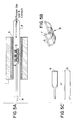
- FIG. 5A is a schematic illustration of a typical semiconductor diffusion furnace.
- FIG. 5B is an enlarged schematic view of the wafer boat furniture used in the FIG. 5A furnace.
- FIG. 5C is an enlarged view of the cantilever paddle or rod-type furniture used in the FIG. 5A furnace.
- FIG. 6A is a top schematic view of a typical pancake susceptor for handling semiconductor wafers.
- FIG. 6B is a cross-sectional view of the susceptor through plane A-A of FIG. 6A.
- FIG. 7 is a schematic illustration of a typical vacuum chuck for handling semiconductor wafers.
- FIG. 8A is a top schematic view of a typical transport ring for handling semiconductor wafers.
- FIG. 8B is a cross-sectional view of the transport ring through plane B-B of FIG. 8A.
- the present invention provides ultra pure SiC having a total impurity level of about 5 ppm or less, preferably less than about 3.5 ppm, by weight as measured by glow discharge mass spectroscopy (GDMS).
- the total impurity level constitutes the sum of all the metal, metalloid and non-metal elements shown in Table 1 below; namely, aluminum (Al), arsenic (As), boron (B), calcium (Ca), cadmium (Cd), chromium (Cr), copper (Cu), iron (Fe), potassium (K), lithium (Li), magnesium (Mg), manganese (Mn), sodium (Na), nickel (Ni), phosphorus (P), antimony (Sb), titanium (Ti) and zirconium (Zr).
- Table 1 below
- Al aluminum
- B calcium
- Ca cadmium
- Cr chromium
- Cu copper
- K lithium
- Li magnesium
- Mn manganese
- the SiC produced according to the invention is stoichiometric (1:1 Si:C ratio), has a cubic ( ⁇ ) polycrystalline structure, is 100% theoretically dense, has very high thermal conductivity, high strength, excellent thermal shock resistance and excellent thermal stability.
- Thermal conductivity is strongly dependent on the grain size and purity of the SiC, i.e., the thermal conductivity increases with increasing grain size and low impurity concentration along the grain boundaries.
- the grain size and, therefore, the thermal conductivity is controlled, for example, by the deposition temperature, pressure, and gas flow rates. For example, under conditions of high temperature and low MTS flow rate (which results in low MTS partial pressure), the grain size increases. Conversely, as the temperature is lowered and the MTS flow increases, the grain size decreases.
- SiC produced in accordance with the invention has a thermal conductivity of about 300 W/mK or above.
- the SiC can be produced in various free-standing sizes and shapes, having particular application for high temperature semiconductor processing equipment, e.g. furnace furniture and semiconductor wafer handling components, and does not need to be coated, laminated, etc, with other materials.
- SiC is pyrolytically produced by chemical vapor deposition (CVD) in the form of free-standing, bulk bodies of such a purity not heretofore achievable using very specific and controlled process conditions. Certain parameters, such as individual gas flow rates may vary according to the size and design of the particular CVD furnace.
- CVD-SiC structures having the aforementioned impurity level as well as a thermal conductivity of at least about 300 W/mk, is preferably pyrolytically deposited in a CVD furnace having a removable mandrel on which deposition takes place under very strict reaction conditions using the gas mixture consisting of at least methyltrichlorosilane (MTS) and H2; in particular: a furnace pressure of between about 180 and about 220 torr, a deposition temperature of between about 1340 and about 1380°C, preferably between about 1340 and about 1370°C, and most preferably about 1350°C, a deposition rate of between about 1.0 and about 2.0 ⁇ m/min., and an H2/MTS molar ratio of between about 4 and 10.
- MTS methyltrichlorosilane
- H2 supplied as a part of the gas stream is purified so that it contains less than about 1 part per million (ppm) 02 gas by weight and various means and techniques are provided to exclude particulate contaminant material from the deposition chamber.
- the gas mixture almost always includes an inert gas, preferably argon, as a carrier for MTS and in an amount to adjust aerodynamic properties of the gas stream.
- an inert gas preferably argon
- the process might be run using only MTS carried by H2.
- deposition chamber temperature what is meant herein is the temperature as determined in the deposition chamber in close proximity to the mandrel on which the silicon carbide is being deposited, although the actual mandrel temperature may be slightly different. Experience has shown that temperatures at different locations relative to, but each closely adjacent the mandrel seldom vary more than about 5°C, and it is assumed that the actual deposition temperature at the mandrel is within 10°C of the probed temperature.
- Thermal conductivity is believed to be relatively consistent, regardless of method of measurement.
- thermal conductivity is the thermal conductivity as typically measured by flash lamp techniques.
- the monolithic (bulk), free-standing SiC produced is preferably at least 5/1000 inch thick (0.127mm).
- the SiC is preferably deposited to a thickness of at least about 1-3 mm.
- the SiC body or structure may be partially configured according to the particular mandrel on which SiC is deposited, but is generally further configured and/or finished by machine tooling following deposition.
- Free-standing SiC signifies a body that is capable of standing free or on its own, and is to be distinquished from SiC thin film coatings (currently its most common application) which are required to be supported by and inseparable from a backing material or layer.
- SiC is capable of being handled or manipulated without a backing support for such subsequent processing as machining and polishing, if required, in much the same fashion as RB or sintered castings of SiC.
- the SiC body may be polished on a surface or surfaces according to the requirements of the particular component part made by such conventional means as lapping using pitch and progressively finer diamond abrasive.
- FIG. 1 Illustrated in Fig. 1 is a diagrammatic cross-sectional illustration of a 0.5-m CVD-SiC furnace 10 adapted for depositing ultra pure, highly thermal conductive SiC according to the invention.
- the apparatus includes an outer wall or housing comprising a cylindrical sidewall 11, a top plate 12 and a bottom plate 14.
- An inner wall or housing comprises a cylindrical sidewall (or isolation tube) 16, a top cover 18 and a bottom cover 20; the inner wall defines the inner space which is the deposition chamber 22.
- Surrounding the isolation tube 16 is a side heater 24; below the bottom cover 20 is a bottom heater 26.
- Each of the heaters 24, 26 are of the electrical resistive type, e.g., being formed of graphite glow bars.
- insulating material 28 Interposed between the inner housing and outer housing and surrounding the inner housing and heaters 24, 26 are layers of insulating material 28 which are usually formed of fibrous material, e.g., carbon fibers.
- these carbon fiber layers 28 are a source of particulate material, for example, during furnace assembly; and means are provided for blocking the carbon fibers as a source of particulate material, for example, during furnace assembly; and means are provided for blocking the carbon fibers as a source of particulate material to the deposition chamber.
- Injector means 30 provide for entry of gas through the upper end of the furnace and to the deposition chamber. In the illustrated furnace 10, three injector tubes 30 are illustrated. As will be explained in greater detail with respect to Fig.
- the injectors are a potential source of particulates, including relatively large particulates, and the injectors 30 in the illustrated furnace have been modified from previous injector design to eliminate the injectors 30 as a source of particulate material in the deposition chamber 22.
- An exhaust tube 32 communicates with the lower end of the deposition chamber 22.
- a baffle plate 34 which is supported just above the bottom cover 22 in a horizontal orientation. Supported above the baffle plate 34, also in a horizontal orientation, is the mandrel 36 on which the bulk CVD SiC is deposited. Deposition chamber 22 temperature is monitored by thermocouples 38 and optical pyrometers 40.
- the furnace is assembled through the bottom between each run.
- protective ceramic blankets or covers 42 are provided over the carbon felt layers 28.
- the cover means 42 illustrated in Fig. 2 comprise cover sheets of nonporous ceramic gasket material, for example graphite, such as that sold under the tradename Graffoil, and carbon sleeves 44 capping orifices through the layers 28.
- each injector 30 is comprised of three concentric tubes which define annular passageways 56 and 58 and a central passageway 60.
- the central passageway 60 is the gas passageway and is open at its lower end to communicate with the deposition chamber 22.
- An annular cap 62 extends between the outer and inner tubes 50,54 sealing the lower end of the annular passageways 56,58 to each other.
- the lower end of the middle tube 52 is spaced above the annular cap 62 to provide a gap 64 that communicates the annular passageways 56,58.
- a coolant usually water, is pumped downward through the inner annular passageway 58 and returns through the outer annular passageway 56. This coolant prevents deposition from occurring in the gas flow passageway 60 in the heated region where it communicates with the deposition chamber 22 by keeping the passageway 60 below the deposition temperature.
- each injector tube 30 must be movable relative to at least the top plate or cover 12 of the outer housing or the top cover 18 of the inner housing because of the different temperatures of each of the housings and the resulting difference in expansion and contraction during furnace operation.
- the lower end of the injector tubes extended downward below the top cover 18 of the inner housing and into the deposition chamber 22 to ensure continual communication between the central passage of the injector and the deposition chamber. This was found to be problematic in that the cooler injectors tended to promote condensation and film build-up thereon, which deposition might flake off and fall onto the mandrel 36 therebelow and become large particulate inclusions in the SiC being deposited thereon.
- the injector tubes 30 have been positioned or adapted to extend downward to, but not into, the deposition chamber 22, providing continuous communication with the deposition chamber, while being relatively slidable relative to the top plate 12 of the outerhousing. Illustrated in Fig.2 is a preferred design for injector apparatus which provides for each injector tube 30 extending to, but not into, the deposition chamber 22.
- An inlet opening 70 in the top cover 18 of the inner housing is shaped to provide an annular ledge 72. Seated in the opening 70 on the ledge 72 is a carbon washer 74 of appropriate interior diameter that each injection tube 30 seats thereontop.
- a tubular carbon guide 76 having a tapered upper end 78 also is seated in the opening 70 on the washer 72.
- Each injector tube 30 extends upwards through openings 80, 82 in the insulation 28 and top plate 12.
- a flanged sleeve 84 is provided at the opening 82, fixed to the top plate 12.
- Each injector tube 30 is vertically movable through the flanged sleeve 84 to accommodate differential thermal expansion of the inner and outer housings.
- a coupling 86 is provided around each injector tube 30 at a location above the top plate 12. Providing a seal between the coupling 86 and the flanged sleeve 34 is a bellows 90 that accommodates relative vertical movement between the top plate 12 and each injector tube 30.
- the illustrated bellows provides for attachment and separation 88 at two points; 0-rings 88 at these points provide a gas-tight seal during operation.
- Fig. 4 is a schematic of a hydrogen gas line 99 which has been modified to eliminate oxygen and some other gaseous impurities continuously from the H2 introduced.
- the hydrogen gas line confluences with a flow of argon-carried MTS (not shown), and the combined flow of argon, hydrogen and MTS is introduced into the deposition chamber 22 through the injectors 30.
- the gas line includes the hydrogen source 100. Downstream from the hydrogen source 100 is a catalytic purifier 102, such as Resource Systems, Inc., Model RCP-500, which converts oxygen to water. Downstream of the catalytic purifier 102 is a molecular sieve dryer 104, such as Resource Systems, Inc., Model MSD-1000, which traps the water.
- This system reduces the oxygen content of the hydrogen gas stream to below 1 ppm.
- This system is also capable of removing carbon dioxide, ammonia and other undesirable polar molecules.
- this system represents the preferred method of removing O2 from the H2 gas stream, other means, such as a gettering system, could be employed for this purpose.
- Fig. 5A is a schematic of a well known type high temperature diffusion furnace 1 used in the processing of wafers 2, e.g. silicon, to make semiconductor devices.
- the major components of this process system are: (1) furnace liner 3, (2) process tube 4, (3) wafer boats 5 and (4) cantilever system 8.
- the furnace liner 3 is an open ended tube which acts as a barrier to separate the process tube 4 from the diffusion furnace 1.
- the furnace liner 3 is usually about 65 inches long and aids in preventing diffusion of impurities which, for example, outgas from the hot furnace walls, heating elements, etc., into the process tube 4.
- the process tube 4 is a closed end tube, typically about 120 inches long, with gas inlet and exhaust ports at the closed end and an openable flange at the opposite end.
- Wafers 2 are loaded into the flanged end of the process tube, when opened, then sealed in the tube whereupon the tube is heated and gases are metered into the tube. Certain of the gaseous elements diffuse into the wafers at high temperatures to obtain the desired electrical properties, and any by-products of the process exit through the exhaust port. Wafers 2 are held inside the process tube 4 in what are known as wafer boats 5.
- Fig. 5B is an enlarged schematic view of a typical wafer boat as depicted in Fig. 5A. There are numerous well known boat designs, which are usually about 6 inches long; however, all of the different designs have a common feature of holding a plurality of wafers in evenly spaced slots 6 machined into the walls or rails 7 of the boats.
- the cantilever system 8 is used to load and unload the wafer boats 5 into the process tube 4.
- the cantilever system uses either a paddle 9 or parallel rods 13 (two per set) mounted to an end cover plate (not shown) onto which the wafer boats sit during loading, processing and unloading.
- Fig. 5C illustrates an enlarged view of the cantilever paddle or rods schematically depicted in Fig. 5A.
- the wafer boats 5 are placed on the paddle 9 or rods 13 and then slid into the process tube 4 on a rail system (not shown).
- the cantilever and cover plate is then sealed to the process tube flange (open end).
- Fig. 6A is a top view of a well known pancake type susceptor 45 having a central opening for handling semiconductor wafers.
- Fig. 6B is a cross-sectional view of disc shaped susceptor plate 45 shown in Fig. 6A through plane A-A.
- Susceptors are typically used to heat wafers, e.g. silicon, during various processes known in the art for making semiconductor devices.
- a plurality of wafers are typically placed in recessed pockets 46 (seven are shown) in the susceptor plate, which is then loaded into a processing chamber (not shown), typically made of quartz.
- the wafers are then heated, for example, by coupling electromagnetic energy (usually RF or infrared energy) into the susceptor plate which heats the plate and wafers.
- electromagnetic energy usually RF or infrared energy
- Fig. 7 is a schematic illustration of a vacuum chuck 47 for handling semiconductor wafers 2 which are frequently transported robotically from one process station to another.
- the vacuum chuck is perforated and made of a lightweight, stiff, high purity material, as previously indicated, that can be fabricated with an optically flat surface. Also the material should maintain its flatness after repeated heating and cooling cycles during processing.
- Fig. 8A is a top schematic view of a typical transport ring 48 having a central opening for handling semiconductor wafers.
- a cross-sectional view through plane B-B of Fig. 8A is shown of the transport ring 48 in Fig. 8B.
- the transport ring is a fixture to support a wafer during processing and transport from one process station to another.
- the transport ring material should be highly pure to prevent contamination of the wafer during semiconductor processing, exhibit good thermal stability, be light weight and strong, and machinable to high tolerances.
- the ultra high purity CVD-SiC produced in bulk according to the invention satisfies the above identified criteria, and it has been found to be especially applicable stock material for fabricating the above mentioned furnace furniture and wafer handling equipment in place of the prior art materials previously discussed.
- the benefits of such a substitution include: (1) reduction of undesirable contaminants in semiconductor devices, (2) more reliable semiconductor devices, (3) lower semiconductor processing costs and (4) improved semiconductor device performance.
- the CVD-SiC according to the invention has special application as dummy wafers in which purity is a critical requirement.
- various contaminants can diffuse into or onto the semiconductor product wafers during processing and adversely change their electrical and optical properties.
- any alkali metal and iron ions would be treated as impurities and should be avoided.
- Group II and IV trace impurities would be considered detrimental to III-V compound semiconductors.
- Dummy wafers are used, for example, as filler wafers and for monitoring and test purposes. In the filler application, the empty spaces in a boat carrying product wafers may be filled with dummy (false or imitation) wafers.
- the CVD-SiC according to the invention has special application as sputtering targets, evaporation sources and evaporation crucibles or boats which are used in many physical vapor deposition (PVD) systems for depositing thin films and coatings.
- PVD physical vapor deposition
- CVD-SiC has greater than an order of magnitude (factor of 10) less trace element impurities than the GE quartz and approximately two orders of magnitude (factor of 100) less than the Norton SiC.
- the CVD-SiC according to the invention has been analyzed at different testing laboratories on the same sample, and these results show that total impurity level is very low, i.e. less than about 5 ppm, and even less than 3.5 ppm, by weight. Similar results have been obtained on numerous samples from different CVD runs and different furnaces, i.e. a small research size furnace and larger 0.5-m and 1.5-m production furnaces.
- CVD-SiC is deposited in accordance with the conditions described in aforementioned U.S. Pat. No. 4,990,374, column 1,lines 30-36, i.e.: deposition temperature 1300°C, furnace pressure 200 torr, gas partial pressures Ar 68 torr, H2 102 torr and MTS 30 torr.
- deposition temperature 1300°C furnace pressure 200 torr
- the following table compares properties of the SiC deposited using the conditions in Example 1 with the SiC deposited in accordance with said patent. (Values specified room temperature measurement values (20-25°C).
- CVD-SiC was deposited in a 0.5mm furnace under the following conditions: Furnace Pressure, (torr) 200 Deposition Temperature, °C 1350 Gas Flow Rates: (slpm) H2 28 Ar 77 MTS 5.9 Gas Partial Pressures: (torr) H2 50 Ar 139 MTS 10.6 Deposition Rate, ⁇ m/min 1.5 H2/MTS Gas Flow Ratio 4.7
- the CVD-SiC produced has a total impurity level (see Table 1) of less than about 3.5 ppm by wt. and a thermal conductivity of 304.9 W/mK at 28°C (301°K) and polishable to ⁇ 1 ⁇ RMS.
Landscapes
- Chemical & Material Sciences (AREA)
- Engineering & Computer Science (AREA)
- Materials Engineering (AREA)
- Organic Chemistry (AREA)
- General Chemical & Material Sciences (AREA)
- Chemical Kinetics & Catalysis (AREA)
- Mechanical Engineering (AREA)
- Metallurgy (AREA)
- Ceramic Engineering (AREA)
- Inorganic Chemistry (AREA)
- Manufacturing & Machinery (AREA)
- Structural Engineering (AREA)
- Chemical Vapour Deposition (AREA)
- Ceramic Products (AREA)
- Manufacturing Of Tubular Articles Or Embedded Moulded Articles (AREA)
- Crystals, And After-Treatments Of Crystals (AREA)
- Carbon And Carbon Compounds (AREA)
Applications Claiming Priority (8)
| Application Number | Priority Date | Filing Date | Title |
|---|---|---|---|
| US92307792A | 1992-07-31 | 1992-07-31 | |
| US923077 | 1992-07-31 | ||
| US959880 | 1992-10-13 | ||
| US07/959,880 US5374412A (en) | 1992-07-31 | 1992-10-13 | Highly polishable, highly thermally conductive silicon carbide |
| US97996592A | 1992-11-23 | 1992-11-23 | |
| US979965 | 1992-11-23 | ||
| US5860893A | 1993-05-06 | 1993-05-06 | |
| US58608 | 1993-05-06 |
Publications (1)
| Publication Number | Publication Date |
|---|---|
| EP0582444A1 true EP0582444A1 (de) | 1994-02-09 |
Family
ID=27489997
Family Applications (1)
| Application Number | Title | Priority Date | Filing Date |
|---|---|---|---|
| EP93306021A Withdrawn EP0582444A1 (de) | 1992-07-31 | 1993-07-30 | Ultrareines Siliziumkarbid und daraus hergestellte Hochtemperaturbearbeitungseinrichtung für Halbleiter |
Country Status (4)
| Country | Link |
|---|---|
| EP (1) | EP0582444A1 (de) |
| JP (1) | JPH06206718A (de) |
| CA (1) | CA2099788A1 (de) |
| IL (1) | IL106418A0 (de) |
Cited By (19)
| Publication number | Priority date | Publication date | Assignee | Title |
|---|---|---|---|---|
| EP0770704A1 (de) * | 1995-10-27 | 1997-05-02 | Shin-Etsu Handotai Company Limited | Verfahren zur Herstellung einer Dünnschicht |
| WO1997022967A1 (en) * | 1995-12-20 | 1997-06-26 | Minnesota Mining And Manufacturing Company | Ceramic wafers and thin film magnetic heads |
| EP0787822A1 (de) * | 1996-01-30 | 1997-08-06 | Siemens Aktiengesellschaft | Verfahren und Vorrichtung zum Herstellen von SiC durch CVD mit verbesserter Gasausnutzung |
| WO1998039270A1 (en) * | 1997-03-03 | 1998-09-11 | Saint-Gobain Industrial Ceramics, Inc. | Hot pressed silicon carbide wafer and method of using it as a dummy wafer |
| EP0935013A1 (de) * | 1998-02-09 | 1999-08-11 | Tokai Carbon Company, Ltd. | Produkt aus SiC und Verfahren zu seiner Herstellung |
| EP1043420A1 (de) * | 1999-04-07 | 2000-10-11 | Ngk Insulators, Ltd. | Siliziumkarbid-Formkörper |
| EP1127955A1 (de) * | 2000-02-24 | 2001-08-29 | Shipley Company LLC | Siliziumkarbid mit geringem Widerstand |
| EP0986102A3 (de) * | 1998-04-21 | 2002-03-06 | Thomas Milton Sullivan | Polykristalline Siliziumkarbidkeramikscheibe und Substrat |
| US6436361B1 (en) | 1999-07-30 | 2002-08-20 | Asahi Glass Company, Limited | Silicon carbide and process for its production |
| EP1289002A2 (de) * | 2001-07-16 | 2003-03-05 | Shipley Co. L.L.C. | Halbleiterscheibehaltevorrichtung |
| US6939821B2 (en) | 2000-02-24 | 2005-09-06 | Shipley Company, L.L.C. | Low resistivity silicon carbide |
| US7501370B2 (en) * | 2004-01-06 | 2009-03-10 | Saint-Gobain Ceramics & Plastics, Inc. | High purity silicon carbide wafer boats |
| US8058174B2 (en) | 2007-12-20 | 2011-11-15 | Coorstek, Inc. | Method for treating semiconductor processing components and components formed thereby |
| US20150072100A1 (en) * | 2013-09-06 | 2015-03-12 | Sumitomo Electric Industries, Ltd. | Silicon carbide epitaxial substrate and method of manufacturing silicon carbide epitaxial substrate |
| AT518081A4 (de) * | 2015-12-22 | 2017-07-15 | Sico Tech Gmbh | Injektor aus Silizium für die Halbleiterindustrie |
| WO2019224098A1 (de) | 2018-05-22 | 2019-11-28 | Sico Technology Gmbh | Injektor aus silizium für die halbleiterindustrie |
| US11049747B2 (en) | 2019-02-28 | 2021-06-29 | Admap Inc. | SiC freestanding film structure |
| CN114890819A (zh) * | 2022-05-30 | 2022-08-12 | 无锡海飞凌半导体材料有限公司 | 一种陶瓷表面碳化硅涂层的工艺 |
| US20230042832A1 (en) * | 2019-06-21 | 2023-02-09 | Tokai Carbon Korea Co., Ltd | Sic structure formed by cvd method |
Families Citing this family (10)
| Publication number | Priority date | Publication date | Assignee | Title |
|---|---|---|---|---|
| JPH1179846A (ja) * | 1997-09-01 | 1999-03-23 | Tokai Carbon Co Ltd | 炭化珪素成形体 |
| JP4595153B2 (ja) * | 2000-02-14 | 2010-12-08 | 旭硝子株式会社 | 炭化ケイ素体およびその製造方法 |
| US6699401B1 (en) | 2000-02-15 | 2004-03-02 | Toshiba Ceramics Co., Ltd. | Method for manufacturing Si-SiC member for semiconductor heat treatment |
| JP2002003275A (ja) * | 2000-06-20 | 2002-01-09 | Tokai Carbon Co Ltd | 光不透過性SiC成形体及びその製造方法 |
| US20040173597A1 (en) * | 2003-03-03 | 2004-09-09 | Manoj Agrawal | Apparatus for contacting gases at high temperature |
| JP2006269820A (ja) * | 2005-03-24 | 2006-10-05 | Toyoko Kagaku Co Ltd | 半導体熱処理炉用炉心管 |
| EP1863079B1 (de) | 2006-06-02 | 2011-08-10 | Rohm and Haas Electronic Materials, L.L.C. | Vorrichtung mit Verbindungen mit ausgebuchtetem Radius |
| JP4880624B2 (ja) * | 2008-01-28 | 2012-02-22 | 東洋炭素株式会社 | 気相成長用サセプター及びその製造方法 |
| SG2014012835A (en) * | 2009-02-12 | 2014-04-28 | Univ Griffith | A chemical vapour deposition system and process |
| JP6609300B2 (ja) * | 2017-12-21 | 2019-11-20 | 國家中山科學研究院 | 特定形状の炭化ケイ素の育成装置 |
Citations (3)
| Publication number | Priority date | Publication date | Assignee | Title |
|---|---|---|---|---|
| US4123989A (en) * | 1977-09-12 | 1978-11-07 | Mobil Tyco Solar Energy Corp. | Manufacture of silicon on the inside of a tube |
| JPH0323209A (ja) * | 1989-06-21 | 1991-01-31 | Toyo Tanso Kk | 炭素質成形断熱体 |
| EP0494753A2 (de) * | 1991-01-07 | 1992-07-15 | Cvd Incorporated | Durch CVD hergestelltes Silicium und Siliciumkarbid mit verbesserten optischen Eigenschaften |
Family Cites Families (3)
| Publication number | Priority date | Publication date | Assignee | Title |
|---|---|---|---|---|
| JPH01282153A (ja) * | 1988-05-06 | 1989-11-14 | Shin Etsu Chem Co Ltd | 炭化珪素質反応管 |
| JPH03252307A (ja) * | 1990-02-27 | 1991-11-11 | Showa Denko Kk | 多結晶炭化珪素 |
| JPH0492447A (ja) * | 1990-08-08 | 1992-03-25 | Shin Etsu Chem Co Ltd | 無機薄膜の成膜方法 |
-
1993
- 1993-07-05 CA CA002099788A patent/CA2099788A1/en not_active Abandoned
- 1993-07-20 IL IL106418A patent/IL106418A0/xx unknown
- 1993-07-30 JP JP5189715A patent/JPH06206718A/ja active Pending
- 1993-07-30 EP EP93306021A patent/EP0582444A1/de not_active Withdrawn
Patent Citations (3)
| Publication number | Priority date | Publication date | Assignee | Title |
|---|---|---|---|---|
| US4123989A (en) * | 1977-09-12 | 1978-11-07 | Mobil Tyco Solar Energy Corp. | Manufacture of silicon on the inside of a tube |
| JPH0323209A (ja) * | 1989-06-21 | 1991-01-31 | Toyo Tanso Kk | 炭素質成形断熱体 |
| EP0494753A2 (de) * | 1991-01-07 | 1992-07-15 | Cvd Incorporated | Durch CVD hergestelltes Silicium und Siliciumkarbid mit verbesserten optischen Eigenschaften |
Non-Patent Citations (4)
| Title |
|---|
| DATABASE WPI Derwent World Patents Index; AN 91-076960 Ç11 * |
| JACOBSON K A: "Growth, texture, and surface morphology of SiC layers", JOURNAL OF THE ELECTROCHEMICAL SOCIETY, vol. 118, no. 6, June 1971 (1971-06-01), USA, pages 1001 - 1006, XP001309490 * |
| P. LIAW ET AL.: "EPITAXIAL GROWTH AND CHARACTERIZATION OF BETA SIC THIN FILMS", JOURNAL OF THE ELECTROCHEMICAL SOCIETY, vol. 132, no. 3, March 1985 (1985-03-01), US, pages 642 - 648 * |
| Y. CHINONE ET AL: "APPLICATIONS OF HIGH PURITY SIC PREPARED BY CHEMICAL VAPOR DEPOSITION", SPRINGER PROCEEDINGS IN PHYSICS, AMORPHOUS AND CRYSTALLINE SILICON CARBIDE AND RELATED MATERIALS II., vol. 43, 16 December 1988 (1988-12-16), BERLIN, pages 198 - 206, XP000617080 * |
Cited By (29)
| Publication number | Priority date | Publication date | Assignee | Title |
|---|---|---|---|---|
| US5858881A (en) * | 1995-10-27 | 1999-01-12 | Shin-Etsu Handotai Co., Ltd. | Method of producing thin film |
| EP0770704A1 (de) * | 1995-10-27 | 1997-05-02 | Shin-Etsu Handotai Company Limited | Verfahren zur Herstellung einer Dünnschicht |
| WO1997022967A1 (en) * | 1995-12-20 | 1997-06-26 | Minnesota Mining And Manufacturing Company | Ceramic wafers and thin film magnetic heads |
| US5670253A (en) * | 1995-12-20 | 1997-09-23 | Minnesota Mining And Manufacturing Company | Ceramic wafers and thin film magnetic heads |
| EP0787822A1 (de) * | 1996-01-30 | 1997-08-06 | Siemens Aktiengesellschaft | Verfahren und Vorrichtung zum Herstellen von SiC durch CVD mit verbesserter Gasausnutzung |
| US6299683B1 (en) | 1996-01-30 | 2001-10-09 | Siemens Aktiengesellschaft | Method and apparatus for the production of SiC by means of CVD with improved gas utilization |
| WO1998039270A1 (en) * | 1997-03-03 | 1998-09-11 | Saint-Gobain Industrial Ceramics, Inc. | Hot pressed silicon carbide wafer and method of using it as a dummy wafer |
| EP0935013A1 (de) * | 1998-02-09 | 1999-08-11 | Tokai Carbon Company, Ltd. | Produkt aus SiC und Verfahren zu seiner Herstellung |
| EP0986102A3 (de) * | 1998-04-21 | 2002-03-06 | Thomas Milton Sullivan | Polykristalline Siliziumkarbidkeramikscheibe und Substrat |
| US6479174B1 (en) | 1999-04-07 | 2002-11-12 | Ngk Insulators, Ltd. | Silicon carbide body |
| EP1043420A1 (de) * | 1999-04-07 | 2000-10-11 | Ngk Insulators, Ltd. | Siliziumkarbid-Formkörper |
| US6436361B1 (en) | 1999-07-30 | 2002-08-20 | Asahi Glass Company, Limited | Silicon carbide and process for its production |
| US6939821B2 (en) | 2000-02-24 | 2005-09-06 | Shipley Company, L.L.C. | Low resistivity silicon carbide |
| EP1127955A1 (de) * | 2000-02-24 | 2001-08-29 | Shipley Company LLC | Siliziumkarbid mit geringem Widerstand |
| US7018947B2 (en) | 2000-02-24 | 2006-03-28 | Shipley Company, L.L.C. | Low resistivity silicon carbide |
| KR100760342B1 (ko) * | 2000-02-24 | 2007-09-20 | 롬 앤드 하스 일렉트로닉 머트어리얼즈, 엘.엘.씨 | 저 저항성 실리콘 카바이드 |
| US7927915B2 (en) | 2000-02-24 | 2011-04-19 | Rohm And Haas Company | Low resistivity silicon carbide |
| EP1289002A2 (de) * | 2001-07-16 | 2003-03-05 | Shipley Co. L.L.C. | Halbleiterscheibehaltevorrichtung |
| US7501370B2 (en) * | 2004-01-06 | 2009-03-10 | Saint-Gobain Ceramics & Plastics, Inc. | High purity silicon carbide wafer boats |
| US8058174B2 (en) | 2007-12-20 | 2011-11-15 | Coorstek, Inc. | Method for treating semiconductor processing components and components formed thereby |
| US9057147B2 (en) * | 2013-09-06 | 2015-06-16 | Sumitomo Electric Industries, Ltd. | Silicon carbide epitaxial substrate and method of manufacturing silicon carbide epitaxial substrate |
| US20150072100A1 (en) * | 2013-09-06 | 2015-03-12 | Sumitomo Electric Industries, Ltd. | Silicon carbide epitaxial substrate and method of manufacturing silicon carbide epitaxial substrate |
| AT518081A4 (de) * | 2015-12-22 | 2017-07-15 | Sico Tech Gmbh | Injektor aus Silizium für die Halbleiterindustrie |
| AT518081B1 (de) * | 2015-12-22 | 2017-07-15 | Sico Tech Gmbh | Injektor aus Silizium für die Halbleiterindustrie |
| WO2019224098A1 (de) | 2018-05-22 | 2019-11-28 | Sico Technology Gmbh | Injektor aus silizium für die halbleiterindustrie |
| US11049747B2 (en) | 2019-02-28 | 2021-06-29 | Admap Inc. | SiC freestanding film structure |
| US20230042832A1 (en) * | 2019-06-21 | 2023-02-09 | Tokai Carbon Korea Co., Ltd | Sic structure formed by cvd method |
| CN114890819A (zh) * | 2022-05-30 | 2022-08-12 | 无锡海飞凌半导体材料有限公司 | 一种陶瓷表面碳化硅涂层的工艺 |
| CN114890819B (zh) * | 2022-05-30 | 2023-11-03 | 无锡海飞凌科技有限公司 | 一种陶瓷表面碳化硅涂层的工艺 |
Also Published As
| Publication number | Publication date |
|---|---|
| JPH06206718A (ja) | 1994-07-26 |
| CA2099788A1 (en) | 1994-02-01 |
| IL106418A0 (en) | 1993-11-15 |
Similar Documents
| Publication | Publication Date | Title |
|---|---|---|
| EP0582444A1 (de) | Ultrareines Siliziumkarbid und daraus hergestellte Hochtemperaturbearbeitungseinrichtung für Halbleiter | |
| US4565747A (en) | Boron nitride containing titanium nitride, method of producing the same and composite ceramics produced therefrom | |
| CA2120092C (en) | Triangular deposition chamber for a vapor deposition system | |
| US5119541A (en) | Wafer succeptor apparatus | |
| EP0588479B1 (de) | Hochglanzpolierbares Siliziumkarbid mit hoher thermischer leitfähigkeit, Verfahren zur Herstellung und Anwendung | |
| US4710428A (en) | Sintered silicon carbide porous body impregnated with metallic silicon | |
| US6300226B1 (en) | Formed SIC product and manufacturing method thereof | |
| CN114000197B (zh) | 气相沉积装置以及使用高纯度聚合物衍生的碳化硅的技术 | |
| EP0229322B1 (de) | Verfahren und Vorrichtung zum Herstellen von Einkristallen nach dem Czochralski-Verfahren | |
| KR101593922B1 (ko) | 화학기상증착법에 의한 반도체 공정용 다결정 탄화규소 벌크 부재 및 그 제조방법 | |
| US4040848A (en) | Polycrystalline silicon articles containing boron by sintering | |
| WO1996029445A1 (en) | Chemical vapor deposition of rhenium on carbon substrates | |
| JPH1012692A (ja) | ダミーウエハ | |
| US6147020A (en) | Light-impermeable, high purity silicon carbide material, a light shielding member for a semiconductor-treating apparatus, and a semiconductor-treating apparatus | |
| WO2021117498A1 (ja) | 炭化タンタル被覆グラファイト部材及びその製造方法 | |
| RU2165999C2 (ru) | Способ формирования защитных покрытий графитовых подложкодержателей и устройство для его осуществления | |
| US4775565A (en) | Vessel for refractory use having multi-layered wall | |
| JP4309509B2 (ja) | 熱分解黒鉛からなる単結晶成長用のルツボの製造方法 | |
| JPH07147277A (ja) | 半導体用部材 | |
| JPH06127922A (ja) | 多結晶シリコン製造用流動層反応器 | |
| JP2002003275A (ja) | 光不透過性SiC成形体及びその製造方法 | |
| JPH1135391A (ja) | 炭化ケイ素被覆サセプタ− | |
| JPH0146454B2 (de) | ||
| JP2719664B2 (ja) | 黒鉛製ウエハ保持治具 | |
| JPS61219787A (ja) | 高純度半導体単結晶製造用ルツボ |
Legal Events
| Date | Code | Title | Description |
|---|---|---|---|
| PUAI | Public reference made under article 153(3) epc to a published international application that has entered the european phase |
Free format text: ORIGINAL CODE: 0009012 |
|
| AK | Designated contracting states |
Kind code of ref document: A1 Designated state(s): CH DE FR GB IT LI NL |
|
| 17P | Request for examination filed |
Effective date: 19940222 |
|
| 17Q | First examination report despatched |
Effective date: 19950321 |
|
| STAA | Information on the status of an ep patent application or granted ep patent |
Free format text: STATUS: THE APPLICATION HAS BEEN WITHDRAWN |
|
| 18W | Application withdrawn |
Withdrawal date: 19950516 |