EP0573164B1 - Full feature high density EEPROM cell with poly tunnel spacer and method of manufacture - Google Patents
Full feature high density EEPROM cell with poly tunnel spacer and method of manufacture Download PDFInfo
- Publication number
- EP0573164B1 EP0573164B1 EP93303793A EP93303793A EP0573164B1 EP 0573164 B1 EP0573164 B1 EP 0573164B1 EP 93303793 A EP93303793 A EP 93303793A EP 93303793 A EP93303793 A EP 93303793A EP 0573164 B1 EP0573164 B1 EP 0573164B1
- Authority
- EP
- European Patent Office
- Prior art keywords
- dielectric material
- layer
- gate
- cell
- regions
- Prior art date
- Legal status (The legal status is an assumption and is not a legal conclusion. Google has not performed a legal analysis and makes no representation as to the accuracy of the status listed.)
- Expired - Lifetime
Links
Images


Classifications
-
- H—ELECTRICITY
- H10—SEMICONDUCTOR DEVICES; ELECTRIC SOLID-STATE DEVICES NOT OTHERWISE PROVIDED FOR
- H10B—ELECTRONIC MEMORY DEVICES
- H10B41/00—Electrically erasable-and-programmable ROM [EEPROM] devices comprising floating gates
-
- H—ELECTRICITY
- H10—SEMICONDUCTOR DEVICES; ELECTRIC SOLID-STATE DEVICES NOT OTHERWISE PROVIDED FOR
- H10D—INORGANIC ELECTRIC SEMICONDUCTOR DEVICES
- H10D30/00—Field-effect transistors [FET]
- H10D30/01—Manufacture or treatment
- H10D30/021—Manufacture or treatment of FETs having insulated gates [IGFET]
- H10D30/0411—Manufacture or treatment of FETs having insulated gates [IGFET] of FETs having floating gates
-
- H—ELECTRICITY
- H10—SEMICONDUCTOR DEVICES; ELECTRIC SOLID-STATE DEVICES NOT OTHERWISE PROVIDED FOR
- H10D—INORGANIC ELECTRIC SEMICONDUCTOR DEVICES
- H10D30/00—Field-effect transistors [FET]
- H10D30/60—Insulated-gate field-effect transistors [IGFET]
- H10D30/68—Floating-gate IGFETs
- H10D30/681—Floating-gate IGFETs having only two programming levels
- H10D30/683—Floating-gate IGFETs having only two programming levels programmed by tunnelling of carriers, e.g. Fowler-Nordheim tunnelling
-
- H—ELECTRICITY
- H10—SEMICONDUCTOR DEVICES; ELECTRIC SOLID-STATE DEVICES NOT OTHERWISE PROVIDED FOR
- H10D—INORGANIC ELECTRIC SEMICONDUCTOR DEVICES
- H10D64/00—Electrodes of devices having potential barriers
- H10D64/01—Manufacture or treatment
- H10D64/013—Manufacture or treatment of electrodes having a conductor capacitively coupled to a semiconductor by an insulator
- H10D64/01302—Manufacture or treatment of electrodes having a conductor capacitively coupled to a semiconductor by an insulator the insulator being formed after the semiconductor body, the semiconductor being silicon
- H10D64/01304—Manufacture or treatment of electrodes having a conductor capacitively coupled to a semiconductor by an insulator the insulator being formed after the semiconductor body, the semiconductor being silicon characterised by the conductor
- H10D64/01326—Aspects related to lithography, isolation or planarisation of the conductor
- H10D64/0133—Aspects related to lithography, isolation or planarisation of the conductor at least part of the entire electrode being a sidewall spacer, being formed by transformation under a mask or being formed by plating at a sidewall
-
- H—ELECTRICITY
- H10—SEMICONDUCTOR DEVICES; ELECTRIC SOLID-STATE DEVICES NOT OTHERWISE PROVIDED FOR
- H10D—INORGANIC ELECTRIC SEMICONDUCTOR DEVICES
- H10D64/00—Electrodes of devices having potential barriers
- H10D64/01—Manufacture or treatment
- H10D64/031—Manufacture or treatment of data-storage electrodes
- H10D64/035—Manufacture or treatment of data-storage electrodes comprising conductor-insulator-conductor-insulator-semiconductor structures
Definitions
- the present invention relates to a high density electrically erasable programmable read only memory (EEPROM) devices and, in particular, to a high density EEPROM cell that is fabricated over a P-well and utilizes a polysilicon floating gate spacer to facilitate Fowler-Nordheim tunneling for programming and erase.
- EEPROM electrically erasable programmable read only memory
- EEPROM electrically erasable programmable read only memory
- the energy difference between the conduction band and the valence band is 1.1 eV.
- silicon dioxide (SiO 2 ) the energy difference between these bands is about 8.1 eV, with the conduction band in SiO 2 3.2 eV above that in Si. Since electron energy is about 0.025 eV at thermal room temperature, the probability that an electron in Si can gain enough thermal energy to surmount the Si-to-SiO 2 barrier and enter the conduction band in SiO 2 is very small. If electrons are placed on a polysilicon floating gate surrounded by SiO 2 , then this band diagram will by itself insure the retention of data.
- Fowler-Nordheim emission which was observed early in this century for the case of electron emission from metals into vacuums, was also observed by Lenzliger and Snow in 1969 for electron emission from silicon to silicon dioxide.
- the energy bands will be distorted and there is a small, but finite, probability that an electron in the conduction band of the Si will quantum mechanically tunnel through the energy barrier and emerge in the conduction band of the SiO 2 .
- This current is observable at a current density of 10E-6 A/cm2 when the field at the Si-SiO 2 interface is about 10 MV/cm.
- the field enhancement arises from textured polysilicon formation, i.e. positive curvature regions at the polysilicon-polysilicon oxide interface resulting in tunneling enhancement at similar voltages as in the first case.
- the theoretically ideal EEPROM memory cell comprises a single transistor addressable by applying electrical signals to a specified row and a specified column of the memory array matrix. For example, to write a logic "1" or a logic “0" into a cell of this "ideal” memory, a voltage is applied to the control gate corresponding to the row (word line) of the selected memory cell while a voltage corresponding to either a logic "1” or a “0” is applied to the source or drain corresponding to the column (bit line) of the selected cell.
- the tunnel dielectric which typically is less than 100 ⁇ thick, is grown over an area defined photolithographically in the drain region (or an extension of the drain region, called buried N+).
- Charging of the floating gate to program the cell is achieved by grounding the source and the drain and applying a high voltage to the control gate.
- the cell is designed such that a large fraction of the applied voltage is coupled across the tunnel oxide, resulting in the transport of electrons from the drain to floating gate.
- Discharge of the floating gate to erase the cell is achieved by grounding the control gate, floating the source and applying a high voltage to the drain.
- the erasing of a cell will mean that high voltage is applied to all drains in a common column. Erasing can be inhibited in non-selected cells by taking unselected word lines to a high voltage. However, this means that unselected cells along the same word line may be programmed. To avoid such disturb conditions, as shown in Fig. 1, the FLOTOX cell utilizes a distinct access transistor to isolate the drain from the column bit line. The access transistor is off for rows that are not selected.
- Fig. 2 provides a layout of the Fig. 1 FLOTOX cell, with the Fig. 1 cross section being taken perpendicular to the word line (control gate) and through the tunnel oxide window.
- the Shelton cell instead of a tunnel oxide area defined lithographically over the drain (buried N+), the Shelton cell has its tunnelling area defined in the channel under the polysilicon floating gate.
- the polysilicon floating gate partially spans the drain side of the channel, while the remainder of the channel (source side) is spanned by an overlying aluminum control gate.
- the aluminum control gate is insulated from the polysilicon floating gate by a thin silicon nitride layer.
- Shelton memory cell is formed in a P-well on a N-substrate. Controlling the P-well potential allows the elimination of the distinct access transistor in each memory cell.
- the potential of the P-well and the sources and drains of the unselected cells are chosen during programming operations to prevent minority carriers from discharging any of the floating gates to the substrate while permitting an individual selected floating gate to be programmed.
- Programming of the Fig. 3 cell is achieved by grounding the P-well and connecting the drain of the memory cell through a load resistance to the programming voltage.
- the source is connected to either the programming voltage or to ground depending upon whether a "1" or a "0" is to be stored.
- the aluminum control gate is connected to the high voltage. If the source potential is also connected to the high voltage, then the internal access transistor doesn't turn on and the surface of the P-well below the floating gate is depleted of electrons. Only a small potential difference exists between the surface of the P-well and the floating gate. Therefore, no electrons tunnel into the gate and the cell remains in a 0 state. If the source terminal is connected to ground (to program a 1), then the internal access transistor turns on, the surface potential under the floating gate drops to close to 0V, and electrons from the inversion layer tunnel through the thin oxide into the floating gate.
- the Fig. 3 cell is erased by grounding the control gate and then raising the P-well to the programming voltage. This causes electrons to tunnel from the floating gate oxide to the P-well via the tunnel oxide. As electrons tunnel through the tunnel oxide, the floating gate acquires a net positive charge.
- Fig. 3 Shelton cell differs from the FLOTOX cell in that it does not utilize a separate access transistor, it does require an internal access transistor and, thus, requires a relatively large cell size.
- the present invention provides a method of fabricating an EEPROM cell as claimed in claim 1 and an EEPROM cell as claimed in claim 8.
- a preferred embodiment of the present invention provides an electrically erasable programmable read only memory (EEPROM) cell that is fabricated by first forming first and second first field oxide (FOX1) regions in a P-well in an N-substrate to define a P-type active device region therebetween. Next, first and second buried N+ bit lines are formed in the P-well adjacent to the first and second FOX1 regions, respectively, such that the first and second N+ bit lines define a P-type channel region therebetween. First and second second field oxide (FOX2) regions are then formed adjacent to the first and second FOX1 regions, respectively, and overlying the first and second buried N+ bit lines, respectively.
- EEPROM electrically erasable programmable read only memory
- a layer of gate oxide about 300-500 ⁇ thick is formed on the P-well between the first and second FOX2 regions.
- a layer of polysilicon is then formed over the gate oxide to extend over only a first portion of the P-type channel region.
- a tunnel window is then defined in the gate oxide over the P-type channel region and overlapping the edge of the floating gate. The gate oxide is removed from this window and tunnel oxide about 80-100 ⁇ thick is grown in the window.
- a spacer/contact window is then defined over the field oxide and overlapping the edge of the floating gate formed on the field oxide. The oxide grown on the edge of the polyl floating gate during tunnel oxide growth is removed from this second window.
- a polysilicon tunnel spacer is then formed over the tunnel oxide and around the perimeter of the floating gate to be in electrical contact with the floating gate at the second window, i.e. at the edge of the floating gate over field oxide;
- oxide is removed from the top of the polyl floating gate plate and from the substrate over the channel region and adjacent to the floating gate.
- ONO is grown over the floating gate, the poly tunnel spacer, and the exposed channel region adjacent the floating gate.
- a second layer of polysilicon and overlying tungsten silicide is formed over the ONO to define a control gate of the EEPROM cell such that the second layer of polysilicon is formed directly on the ONO overlying the second portion of the channel region to thereby define the gate of an internal access transistor of the EEPROM cell.
- Fig. 1 is a cross-section drawing illustrating a conventional EEPROM cell structure that utilizes a distinct access transistor.
- Fig. 2 is a layout illustrating the Fig. 1 cell structure.
- Fig. 3 is a cross-section drawing illustrating a prior art EEPROM cell that is fabricated on a P-well and utilizes an internal access transistor.
- Fig. 4 is a cross-section drawing illustrating a triple-well structure utilizable in the fabrication of an EEPROM cell array in accordance with the present invention.
- Fig. 5 is a cross section drawing illustrating a stage in the fabrication of an EEPROM cell in accordance with the present invention after definition of the cell's N+/N- bit lines.
- Fig. 6 is a cross section drawing illustrating a stage in the fabrication of an EEPROM cell in accordance with the present invention after definition of the cell's floating gate.
- Fig. 7 is a cross-section drawing illustrating a stage in the fabrication of an EEPROM cell in accordance with the present invention after definition of the tunnel window mask.
- Fig. 8 is a cross-section drawing illustrating a stage in the fabrication of an EEPROM cell in accordance with the present invention after growth of the cell's tunnel oxide.
- Fig. 9 is a cross section drawing illustrating a stage in the fabrication of an EEPROM cell in accordance with the present invention after definition of the cell's spacer/contact mask.
- Fig. 10 is a cross-section drawing illustrating a stage in the fabrication of an EEPROM cell in accordance with the present invention after formation of the poly cell's tunnel spacer.
- Fig. 11 is a layout illustrating the Fig. 10 cell structure.
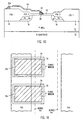
- Fig. 12 is a cross section drawing of an EEPROM cell in accordance with the present invention after formation of the cell's word line.
- Fig. 13 is a layout illustrating the Fig. 12 cell structure.
- Fig. 14 is a cross-section drawing illustrating inhibit conditions in the Fig. 12/13 cell during programming.
- Fig. 15 is a schematic diagram illustrating a portion of a high density EEPROM cell array in accordance with the present invention.
- Figs. 4-12 illustrate the steps for fabricating an EEPROM cell in accordance with the present invention.
- the fabrication process begins with a silicon substrate 10 of N-type conductivity.
- an initial oxide layer (not shown) is grown over the substrate 10.
- a photoresist mask is then formed over the initial oxide layer and patterned to define selected surface areas of the N-type substrate 10. These surface areas are then implanted with a P-type dopant to form P-well regions 12 in the substrate 10.
- the photoresist mask is then stripped from the surface of the oxide and a thermal drive-in step is performed to further define the P-well regions 12.
- the initial oxide layer is then removed from the substrate 10 and a second oxide layer (not shown) is grown over the substrate 10.
- the substrate 10 is again masked with photoresist, which is patterned to define substrate surface areas within those P-well regions 12 which will ultimately contain the peripheral circuitry for the EEPROM memory cell array.
- N-type dopant is implanted into the periphery P-wells 12 to define N-well regions 14.
- the photoresist is then stripped and a further drive-in step for both the N-well regions 14 and the P-well regions 12 is performed. Following the drive-in step, the second oxide layer is removed, resulting in the structure shown in Fig. 4.
- the initial processing steps result in the formation of a triple-well structure which defines the substrate 10 for the formation of the EEPROM memory cell array and its peripheral circuitry.
- the N-well regions 14 in the periphery will be utilized for the fabrication of low voltage (LV) PMOS devices.
- the P-well regions 12 in the periphery will be utilized for the formation of NMOS devices for the peripheral circuitry.
- the P-well regions 12 in the memory cell array portion of the substrate 10 will be utilized for formation of EEPROM storage cell devices.
- the intermediate substrate region will be used for the formation of high voltage (HV) PMOS devices.
- a pad oxide is-first grown on the surface of the substrate 10, followed by deposition of an overlying nitride layer.
- the pad oxide/nitride composite is masked with photoresist, which is then patterned to expose regions of underlying nitride which will ultimately define first field oxide (FOX1) regions.
- the nitride is then etched, the photoresist is stripped and a P-type field implant is performed through the exposed pad oxide regions.
- the field implant mask is then stripped and first field oxide regions (FOX1) 16 are formed, as shown in Fig. 5.
- portions of the P-well regions 12 in the memory cell array are masked, the nitride/oxide composite is etched, and an arsenic implant is performed to define N+ buried bit lines 18 adjacent the FOX1 field oxide regions 16.
- the arsenic implant can be followed by a phosphorous implant to form graded N+/N- bit lines 18, thereby optimizing resistance to avalanche breakdown during the erase of the EEPROM cells.
- the photoresist is then stripped and field oxide growth is completed by formation of second field oxide regions (FOX2) 20 over the N+/N- bit lines 18. Since the bit lines 18 are formed under the field oxide (FOX1/FOX2) 16/20, the size of the device active region can be reduced, resulting in a reduced array size.
- FOX2 second field oxide regions
- the oxide/nitride/oxide (ONO) layer is removed and a sacrificial oxide layer (not shown) is formed.
- a threshold voltage mask is then formed and patterned to expose the channel regions of the N-channel devices of the array.
- a threshold implant is then performed to characterize the threshold voltage of the storage cell transistors and the photoresist mask is stripped. Then the sacrificial oxide is removed.
- a gate oxide layer 22 about 300-500 ⁇ thick is grown over the exposed portions of P-well region 12.
- a first layer of polysilicon is then deposited on the underlying gate oxide 22 to a thickness of about 1500 ⁇ and doped with phosphorous.
- the polysilicon (poly1) is then etched to define the floating gates 24 of the EEPROM cells of the array. As shown in Fig. 6, the polyl floating gate 24 is etched such that it extends from the field oxide 16/20 over only a portion of the P-type channel-region.
- a tunnel window mask is formed over the gate oxide 22 and the floating gate 24 to define a tunnel window 26 that overlaps the edge of the floating gate 24 over the channel.
- the gate oxide in the tunnel window 26 is then etched through to the surface of the P-well 12.
- tunnel oxide 28 about 80-100 ⁇ thick is grown in the tunnel window. This oxidation step also results in the growth of oxide 29 on both the sidewalls and the top of the polyl floating gate 24.
- the structure at this step of the process is shown in Fig. 8.
- a spacer/contact window 30 is defined at the opposite edge of the floating gate 24, i.e. the edge of the floating gate 24 over field oxide.
- the spacer/contact window 30 overlaps the floating gate 24 to provide a region by which a to-be-formed polysilicon spacer will be in electrical contact with the polyl floating gate 24.
- the spacer mask is stripped and a layer of polysilicon is deposited. This layer of polysilicon is then etched back to define a poly tunnel spacer 32 that overlies the tunnel oxide 28 and extends around the perimeter of the floating gate 24 to contact the polyl floating gate 24 over the field oxide (FOX1/FOX2) 16/20.
- the structure at this stage in the process is shown in Fig. 10.
- the poly tunnel spacer 32 is separated from the floating gate 24 by edge oxide except at the spacer contact region 32a.
- tunnel oxide 28 and poly floating gate/spacer combination in this way permits improved process control over the length of extension of the floating gate over the P-type channel region, thereby allowing the channel length and, hence, array size to be reduced.
- oxide is removed from the top of the floating gate 24 and from the channel region adjacent the floating gate 24, a layer 33 of oxide/nitride/oxide composite is then grown over the floating gate 24, the poly tunnel spacer 32 and the exposed portion 35a of the channel region 35 to provide insulation from a subsequently-formed polysilicon word line.
- a protect array mask is formed over the memory cell array portion of the substrate 10 and device formation in the periphery proceeds.
- oxide is etched from the substrate active device regions in the periphery and gate oxide is grown on the active device regions.
- a threshold mask is then formed and a P-type implant is performed to set the threshold of the peripheral PMOS devices.
- the threshold photoresist mask is then stripped and processing begins to form both the word lines for the memory cell array and the gates for the MOS devices in the periphery.
- a second layer of polysilicon is deposited over the surface of the entire device and doped in the conventional manner. This is followed by deposition of an overlying layer of tungsten silicide.
- the poly2/tungsten silicide composite is then masked and etched to define the word lines 34 in the storage cell array and the gate electrodes of the peripheral MOS devices.
- the word lines 34 run parallel to and overly the ONO/poly1 lines in the array.
- the remaining photoresist is then stripped from the device and sidewall oxidation is performed on the devices in the peripheral region.
- FIG. 13 A corresponding layout of the Fig. 12 cell is shown in Fig. 13, with the Fig. 12 cross section being taken along a word line 34 in the Fig. 13 layout.
- the EEPROM memory cell utilizes a polyl floating gate plate 24 which is truncated with an edge over the P-well channel region between N+ buried bit lines 18.
- the overlying poly2 word line 34 forms the gate 36 of an internal access transistor in a manner similar to the Shelton cell described above.
- the Fig. 7 cell is smaller than the Shelton cell.
- the internal access transistor prevents over-erase in the array.
- Table 1 provides a programming scheme for the Fig. 12/13 cell.
- the Table I programming scheme addresses deep depletion during programming by causing any minority carriers (i.e. electrons) thermally generated in the P-well or in the space charge regions to be "sucked up" by the N-/P-well and the bit line/P-well reversed bias junctions.
- the programming conditions are as follows.
- word line WL1 is held at the programming voltage V pp .
- Bit line BL n and bit line BL n1 are held at the low supply voltage V ss .
- the P-well is also held at V ss . This creates an inversion layer of minority carriers in the channel, causing electrons to tunnel to the floating gate.
- cell C is program-inhibited by holding word line WL2 at V ss , bit line BL n and BL n1 at V ss and the P-well at V ss .
- cell B is program inhibited by holding wordline WL1 at V pp and raising bit line BL n+ 1 and BL n'+1 to the programming voltage, while the P-well is held at V ss . This avoids the occurrence of any minority carriers at the P-well surface under the floating gate; the only minority carrier generation is thermal and all of these electrons are evacuated from the P-well by the source and drain and the reverse bias junction.
- the erase conditions for the above-described storage cell are as follows. To erase cell A and its associated byte or word line, word line 1 is held at V ss while bit lines B Ln and B Ln , and B Ln+1 and B Ln'+1 , as well as the P-well are held at the programming voltage Vpp. During this operation, cells C and D are erase inhibited by holding word line WL2 at the programming voltage.
Landscapes
- Non-Volatile Memory (AREA)
- Semiconductor Memories (AREA)
Description
| Source | Drain | Control Gate | P-Well | N-Sub | |
| Write | Vss | Vss | Vpp | Vss | Vpp |
| WL Write Inhibit | Vpp | Vpp | Vpp | Vss | Vpp |
| BL Write Inhibit | Vss | Vss | Vss | Vss | Vpp |
| Erase | Vpp | Vpp | Vss | Vpp | Vpp |
| BL Erase Inhibit | Vpp | Vpp | Vpp | Vpp | Vpp |
| Read | Vss | Vread | Vcc | Vss | Vcc |
Claims (14)
- A method of fabricating an electrically-erasable programmable read only memory (EEPROM) cell in semiconductor material of P-type conductivity the method comprising:(a) forming first and second spaced-apart first field oxide (FOX1) regions in the P-type semiconductor material to define a P-type active device region therebetween;(b) forming first and second spaced-apart bit lines (18) of N-type conductivity in the P-type semiconductor material adjacent to the first and second FOX1 regions, respectively, such that the first and second bit lines define a P-type channel region therebetween;(c) forming first and second spaced-apart second field oxide (FOX2) regions (20) adjacent to the first and second FOX1 regions, respectively, and overlying the first and second bit lines, respectively;(d) forming a layer of gate dielectric material (22) on the P-type semiconductor material between the first and second FOX2 regions;(e) forming a layer of first conductive material (24) over the gate dielectric material to define a floating gate of the EEPROM cell wherein the layer of first conductive material is formed to extend over only a first portion of the P-type channel region;(f) defining tunnel dielectric material (28) in the gate dielectric material over the P-type channel region such that the thickness of the tunnel dielectric material is less than the thickness of the gate dielectric material;(g) forming a tunnel spacer (28) of first conductive material over the tunnel dielectric and in electrical contact with the floating gate;(h) forming a layer of intermediate dielectric material (33) over the floating gate; and(i) forming a layer of second conductive material (34) over the layer of intermediate dielectric material to define a control gate of the EEPROM cell such that the layer of second conductive material is formed directly on intermediate dielectric material overlying a second portion of the channel region to thereby define the gate of an internal access transistor of the EEPROM cell.
- A method as in claim 1 wherein the tunnel dielectric material and the gate dielectric material comprise silicon dioxide.
- A method as in claim 2 wherein the first conductive material comprises polysilicon.
- A method as in claim 3 wherein the intermediate dielectric material comprises an oxide/nitride/oxide composite.
- A method as in claim 4 wherein the second conductive material comprises polysilicon.
- A method as in claim 5 wherein the second conductive material comprises polysilicon and overlying tungsten silicide.
- A method as in claim 1 wherein the P-type semiconductor material comprises a well of P-type conductivity formed in a silicon substrate of N-type conductivity.
- An electrically-erasable programmable read only memory (EEPROM) cell formed in semiconductor material of P-type conductivity, the EEPROM cell comprising:(a) first and second spaced-apart first field oxide (FOX1) regions (16) formed in the P-type semiconductor material to define a P-type active device region therebetween;(b) first and second space-apart bit lines (18) of N-type conductivity formed in the P-type semiconductor material adjacent to the first and second FOX1 regions, respectively, such that the first and second bit lines define a P-type channel region therebetween;(c) first and second spaced-apart second field oxide (FOX2) regions (20) formed adjacent to the first and second FOX1 regions, respectively, and overlying the first and second bit lines, respectively;(d) a layer of gate dielectric material (22) formed on the P-type semiconductor material between the first and second FOX2 regions and having tunnel dielectric material formed therein such that the thickness of the tunnel dielectric material is less than the thickness of the gate dielectric material, the tunnel dielectric being formed over the P-type channel region;(e) a layer of first conductive material (24) formed over the gate dielectric material to define a floating gate of the EEPROM cell and wherein the layer of first conductive material is formed to extend over only a first portion of the P-type channel region.(f) a tunnel spacer of first conductive material (32) formed over the tunnel dielectric and in electrical contact with the floating gate;(g) a layer of intermediate dielectric material (33) formed over the floating gate; and(h) a layer of second conductive material (34) formed over the intermediate dielectric material to define a control gate of the EEPROM cell such that the layer of second conductive material is formed directly on intermediate dielectric material overlying a second portion of the channel region to thereby define the gate of an internal access transistor of the EEPROM cell.
- An EEPROM cell as in claim 8 wherein the tunnel dielectric material and the gate dielectric material comprise silicon dioxide.
- An EEPROM cell as in claim 9 wherein the first conductive material comprises polysilicon.
- An EEPROM cell as in claim 10 wherein the intermediate dielectric material comprises oxide/nitride/oxide composite.
- An EEPROM cell as in claim 11 wherein the second conductive material comprises polysilicon.
- An EEPROM cell as in claim 12 wherein the second conductive material comprises polysilicon and overlying tungsten silicide.
- An EEPROM cell as in claim 8 wherein the P-type semiconductor material comprises a well of P-type conductivity formed in a silicon substrate of N-type conductivity.
Applications Claiming Priority (2)
| Application Number | Priority Date | Filing Date | Title |
|---|---|---|---|
| US891710 | 1986-07-31 | ||
| US07/891,710 US5225362A (en) | 1992-06-01 | 1992-06-01 | Method of manufacturing a full feature high density EEPROM cell with poly tunnel spacer |
Publications (2)
| Publication Number | Publication Date |
|---|---|
| EP0573164A1 EP0573164A1 (en) | 1993-12-08 |
| EP0573164B1 true EP0573164B1 (en) | 1998-07-01 |
Family
ID=25398688
Family Applications (1)
| Application Number | Title | Priority Date | Filing Date |
|---|---|---|---|
| EP93303793A Expired - Lifetime EP0573164B1 (en) | 1992-06-01 | 1993-05-17 | Full feature high density EEPROM cell with poly tunnel spacer and method of manufacture |
Country Status (5)
| Country | Link |
|---|---|
| US (1) | US5225362A (en) |
| EP (1) | EP0573164B1 (en) |
| JP (1) | JPH0685283A (en) |
| KR (1) | KR100316089B1 (en) |
| DE (1) | DE69319384T2 (en) |
Families Citing this family (26)
| Publication number | Priority date | Publication date | Assignee | Title |
|---|---|---|---|---|
| US5364806A (en) * | 1991-08-29 | 1994-11-15 | Hyundai Electronics Industries Co., Ltd. | Method of making a self-aligned dual-bit split gate (DSG) flash EEPROM cell |
| US5379253A (en) * | 1992-06-01 | 1995-01-03 | National Semiconductor Corporation | High density EEPROM cell array with novel programming scheme and method of manufacture |
| JP2682386B2 (en) * | 1993-07-27 | 1997-11-26 | 日本電気株式会社 | Method for manufacturing semiconductor device |
| WO1995025352A1 (en) * | 1994-03-15 | 1995-09-21 | National Semiconductor Corporation | A virtual-ground flash eprom with reduced-step-height field oxide regions in the array |
| US5408115A (en) * | 1994-04-04 | 1995-04-18 | Motorola Inc. | Self-aligned, split-gate EEPROM device |
| US5422504A (en) * | 1994-05-02 | 1995-06-06 | Motorola Inc. | EEPROM memory device having a sidewall spacer floating gate electrode and process |
| US5432112A (en) * | 1994-05-06 | 1995-07-11 | United Microelectronics Corporation | Process for EPROM, flash memory with high coupling ratio |
| US5585293A (en) * | 1994-06-03 | 1996-12-17 | Motorola Inc. | Fabrication process for a 1-transistor EEPROM memory device capable of low-voltage operation |
| US5498559A (en) * | 1994-06-20 | 1996-03-12 | Motorola, Inc. | Method of making a nonvolatile memory device with five transistors |
| US5439838A (en) * | 1994-09-14 | 1995-08-08 | United Microelectronics Corporation | Method of thinning for EEPROM tunneling oxide device |
| US5633518A (en) * | 1995-07-28 | 1997-05-27 | Zycad Corporation | Nonvolatile reprogrammable interconnect cell with FN tunneling and programming method thereof |
| US5521109A (en) * | 1995-09-01 | 1996-05-28 | United Microelectronics Corp. | Method for fabricating a high coupling ratio flash memory with a very narrow tunnel layer |
| DE19534780A1 (en) * | 1995-09-19 | 1997-03-20 | Siemens Ag | Method for producing very small structure widths on a semiconductor substrate |
| US5863819A (en) * | 1995-10-25 | 1999-01-26 | Micron Technology, Inc. | Method of fabricating a DRAM access transistor with dual gate oxide technique |
| US5703808A (en) * | 1996-02-21 | 1997-12-30 | Motorola, Inc. | Non-volatile memory cell and method of programming |
| KR100255512B1 (en) * | 1996-06-29 | 2000-05-01 | 김영환 | Flash memory device manufacturing method |
| US5904524A (en) * | 1996-08-08 | 1999-05-18 | Altera Corporation | Method of making scalable tunnel oxide window with no isolation edges |
| US5998826A (en) * | 1996-09-05 | 1999-12-07 | Macronix International Co., Ltd. | Triple well floating gate memory and operating method with isolated channel program, preprogram and erase processes |
| JP4081854B2 (en) | 1998-05-11 | 2008-04-30 | 沖電気工業株式会社 | Manufacturing method of semiconductor device |
| US6369433B1 (en) * | 1998-10-30 | 2002-04-09 | Advanced Micro Devices, Inc. | High voltage transistor with low body effect and low leakage |
| US6628544B2 (en) | 1999-09-30 | 2003-09-30 | Infineon Technologies Ag | Flash memory cell and method to achieve multiple bits per cell |
| JP4117998B2 (en) * | 2000-03-30 | 2008-07-16 | シャープ株式会社 | Nonvolatile semiconductor memory device, reading, writing and erasing methods thereof, and manufacturing method thereof |
| US6710368B2 (en) * | 2001-10-01 | 2004-03-23 | Ken Scott Fisher | Quantum tunneling transistor |
| US7796442B2 (en) * | 2007-04-02 | 2010-09-14 | Denso Corporation | Nonvolatile semiconductor memory device and method of erasing and programming the same |
| US8446779B2 (en) | 2009-08-21 | 2013-05-21 | Globalfoundries Singapore Pte. Ltd. | Non-volatile memory using pyramidal nanocrystals as electron storage elements |
| CN102136480B (en) * | 2010-01-21 | 2013-03-13 | 上海华虹Nec电子有限公司 | EEPROM (electrically erasable programmable read only memory) device |
Family Cites Families (9)
| Publication number | Priority date | Publication date | Assignee | Title |
|---|---|---|---|---|
| US4258466A (en) * | 1978-11-02 | 1981-03-31 | Texas Instruments Incorporated | High density electrically programmable ROM |
| JPS59119871A (en) * | 1982-12-27 | 1984-07-11 | Fujitsu Ltd | Manufacture of nonvolatile semiconductor memory device |
| IT1191566B (en) * | 1986-06-27 | 1988-03-23 | Sgs Microelettronica Spa | NON-LABELED SEMICONDUCTOR-TYPE MEMORY DEVICE WITH DOOR NOT CONNECTED (FLOATING GATE) ELECTRICALLY ALTERABLE WITH REDUCED TUNNEL AREA AND MANUFACTURING PROCEDURE |
| US4924437A (en) * | 1987-12-09 | 1990-05-08 | Texas Instruments Incorporated | Erasable programmable memory including buried diffusion source/drain lines and erase lines |
| US5156991A (en) * | 1988-02-05 | 1992-10-20 | Texas Instruments Incorporated | Fabricating an electrically-erasable, electrically-programmable read-only memory having a tunnel window insulator and thick oxide isolation between wordlines |
| US4989053A (en) * | 1989-03-27 | 1991-01-29 | Shelton Everett K | Nonvolatile process compatible with a digital and analog double level metal MOS process |
| US5021848A (en) * | 1990-03-13 | 1991-06-04 | Chiu Te Long | Electrically-erasable and electrically-programmable memory storage devices with self aligned tunnel dielectric area and the method of fabricating thereof |
| JPH0451573A (en) * | 1990-06-19 | 1992-02-20 | Mitsubishi Electric Corp | Manufacture of semiconductor device |
| US5108939A (en) * | 1990-10-16 | 1992-04-28 | National Semiconductor Corp. | Method of making a non-volatile memory cell utilizing polycrystalline silicon spacer tunnel region |
-
1992
- 1992-06-01 US US07/891,710 patent/US5225362A/en not_active Expired - Lifetime
-
1993
- 1993-05-17 EP EP93303793A patent/EP0573164B1/en not_active Expired - Lifetime
- 1993-05-17 DE DE69319384T patent/DE69319384T2/en not_active Expired - Lifetime
- 1993-05-31 JP JP5128617A patent/JPH0685283A/en active Pending
- 1993-05-31 KR KR1019930009647A patent/KR100316089B1/en not_active Expired - Lifetime
Also Published As
| Publication number | Publication date |
|---|---|
| KR100316089B1 (en) | 2002-03-21 |
| DE69319384T2 (en) | 1999-02-25 |
| EP0573164A1 (en) | 1993-12-08 |
| DE69319384D1 (en) | 1998-08-06 |
| JPH0685283A (en) | 1994-03-25 |
| KR940001426A (en) | 1994-01-11 |
| US5225362A (en) | 1993-07-06 |
Similar Documents
| Publication | Publication Date | Title |
|---|---|---|
| EP0573170B1 (en) | Method of manufacture of high density EEPROM cell array | |
| EP0573164B1 (en) | Full feature high density EEPROM cell with poly tunnel spacer and method of manufacture | |
| US5687118A (en) | PMOS memory cell with hot electron injection programming and tunnelling erasing | |
| US5293331A (en) | High density EEPROM cell with tunnel oxide stripe | |
| US6101131A (en) | Flash EEPROM device employing polysilicon sidewall spacer as an erase gate | |
| US6608346B2 (en) | Method and structure for an improved floating gate memory cell | |
| US7056785B2 (en) | Non-volatile memory cell fabricated with slight modification to a conventional logic process and methods of operating same | |
| US6143607A (en) | Method for forming flash memory of ETOX-cell programmed by band-to-band tunneling induced substrate hot electron and read by gate induced drain leakage current | |
| US6114724A (en) | Nonvolatile semiconductor memory cell with select gate | |
| US5284786A (en) | Method of making a split floating gate EEPROM cell | |
| US6160286A (en) | Method for operation of a flash memory using n+/p-well diode | |
| US5615152A (en) | Method of erasing a high density contactless flash EPROM array | |
| US5753952A (en) | Nonvolatile memory cell with P-N junction formed in polysilicon floating gate | |
| US5498559A (en) | Method of making a nonvolatile memory device with five transistors | |
| US5889700A (en) | High density EEPROM array using self-aligned control gate and floating gate for both access transistor and memory cell and method of operating same | |
| US5017980A (en) | Electrically-erasable, electrically-programmable read-only memory cell | |
| US5304505A (en) | Process for EEPROM cell structure and architecture with increased capacitance and with programming and erase terminals shared between several cells | |
| US5856222A (en) | Method of fabricating a high density EEPROM cell | |
| US5508955A (en) | Electronically erasable-programmable memory cell having buried bit line | |
| US5780889A (en) | Gate overlap drain source flash structure | |
| US5057446A (en) | Method of making an EEPROM with improved capacitive coupling between control gate and floating gate | |
| US5032533A (en) | Method of making a nonvolatile memory cell with field-plate switch | |
| US6693830B1 (en) | Single-poly two-transistor EEPROM cell with differentially doped floating gate | |
| US6404006B2 (en) | EEPROM cell with tunneling across entire separated channels | |
| US5012307A (en) | Electrically-erasable, electrically-programmable read-only memory |
Legal Events
| Date | Code | Title | Description |
|---|---|---|---|
| PUAI | Public reference made under article 153(3) epc to a published international application that has entered the european phase |
Free format text: ORIGINAL CODE: 0009012 |
|
| AK | Designated contracting states |
Kind code of ref document: A1 Designated state(s): BE CH DE FR GB IT LI NL |
|
| RIN1 | Information on inventor provided before grant (corrected) |
Inventor name: BERGEMONT,ALBERT |
|
| 17P | Request for examination filed |
Effective date: 19940606 |
|
| GRAG | Despatch of communication of intention to grant |
Free format text: ORIGINAL CODE: EPIDOS AGRA |
|
| 17Q | First examination report despatched |
Effective date: 19970814 |
|
| GRAG | Despatch of communication of intention to grant |
Free format text: ORIGINAL CODE: EPIDOS AGRA |
|
| GRAH | Despatch of communication of intention to grant a patent |
Free format text: ORIGINAL CODE: EPIDOS IGRA |
|
| GRAH | Despatch of communication of intention to grant a patent |
Free format text: ORIGINAL CODE: EPIDOS IGRA |
|
| GRAA | (expected) grant |
Free format text: ORIGINAL CODE: 0009210 |
|
| AK | Designated contracting states |
Kind code of ref document: B1 Designated state(s): BE CH DE FR GB IT LI NL |
|
| PG25 | Lapsed in a contracting state [announced via postgrant information from national office to epo] |
Ref country code: NL Free format text: LAPSE BECAUSE OF FAILURE TO SUBMIT A TRANSLATION OF THE DESCRIPTION OR TO PAY THE FEE WITHIN THE PRESCRIBED TIME-LIMIT Effective date: 19980701 Ref country code: LI Free format text: LAPSE BECAUSE OF FAILURE TO SUBMIT A TRANSLATION OF THE DESCRIPTION OR TO PAY THE FEE WITHIN THE PRESCRIBED TIME-LIMIT Effective date: 19980701 Ref country code: IT Free format text: LAPSE BECAUSE OF FAILURE TO SUBMIT A TRANSLATION OF THE DESCRIPTION OR TO PAY THE FEE WITHIN THE PRESCRIBED TIME-LIMIT;WARNING: LAPSES OF ITALIAN PATENTS WITH EFFECTIVE DATE BEFORE 2007 MAY HAVE OCCURRED AT ANY TIME BEFORE 2007. THE CORRECT EFFECTIVE DATE MAY BE DIFFERENT FROM THE ONE RECORDED. Effective date: 19980701 Ref country code: FR Free format text: LAPSE BECAUSE OF FAILURE TO SUBMIT A TRANSLATION OF THE DESCRIPTION OR TO PAY THE FEE WITHIN THE PRESCRIBED TIME-LIMIT Effective date: 19980701 Ref country code: CH Free format text: LAPSE BECAUSE OF FAILURE TO SUBMIT A TRANSLATION OF THE DESCRIPTION OR TO PAY THE FEE WITHIN THE PRESCRIBED TIME-LIMIT Effective date: 19980701 Ref country code: BE Free format text: LAPSE BECAUSE OF FAILURE TO SUBMIT A TRANSLATION OF THE DESCRIPTION OR TO PAY THE FEE WITHIN THE PRESCRIBED TIME-LIMIT Effective date: 19980701 |
|
| REG | Reference to a national code |
Ref country code: CH Ref legal event code: EP |
|
| REF | Corresponds to: |
Ref document number: 69319384 Country of ref document: DE Date of ref document: 19980806 |
|
| EN | Fr: translation not filed | ||
| NLV1 | Nl: lapsed or annulled due to failure to fulfill the requirements of art. 29p and 29m of the patents act | ||
| REG | Reference to a national code |
Ref country code: CH Ref legal event code: PL |
|
| PLBE | No opposition filed within time limit |
Free format text: ORIGINAL CODE: 0009261 |
|
| STAA | Information on the status of an ep patent application or granted ep patent |
Free format text: STATUS: NO OPPOSITION FILED WITHIN TIME LIMIT |
|
| 26N | No opposition filed | ||
| PGFP | Annual fee paid to national office [announced via postgrant information from national office to epo] |
Ref country code: GB Payment date: 20010504 Year of fee payment: 9 |
|
| REG | Reference to a national code |
Ref country code: GB Ref legal event code: IF02 |
|
| PG25 | Lapsed in a contracting state [announced via postgrant information from national office to epo] |
Ref country code: GB Free format text: LAPSE BECAUSE OF NON-PAYMENT OF DUE FEES Effective date: 20020517 |
|
| GBPC | Gb: european patent ceased through non-payment of renewal fee |
Effective date: 20020517 |
|
| PGFP | Annual fee paid to national office [announced via postgrant information from national office to epo] |
Ref country code: DE Payment date: 20120529 Year of fee payment: 20 |
|
| REG | Reference to a national code |
Ref country code: DE Ref legal event code: R082 Ref document number: 69319384 Country of ref document: DE |
|
| REG | Reference to a national code |
Ref country code: DE Ref legal event code: R071 Ref document number: 69319384 Country of ref document: DE |
|
| PG25 | Lapsed in a contracting state [announced via postgrant information from national office to epo] |
Ref country code: DE Free format text: LAPSE BECAUSE OF EXPIRATION OF PROTECTION Effective date: 20130518 |