EP0311695A1 - Force and moment detector using resistor - Google Patents
Force and moment detector using resistor Download PDFInfo
- Publication number
- EP0311695A1 EP0311695A1 EP88903392A EP88903392A EP0311695A1 EP 0311695 A1 EP0311695 A1 EP 0311695A1 EP 88903392 A EP88903392 A EP 88903392A EP 88903392 A EP88903392 A EP 88903392A EP 0311695 A1 EP0311695 A1 EP 0311695A1
- Authority
- EP
- European Patent Office
- Prior art keywords
- axis
- vicinity
- resistance elements
- resistance
- bridge
- Prior art date
- Legal status (The legal status is an assumption and is not a legal conclusion. Google has not performed a legal analysis and makes no representation as to the accuracy of the status listed.)
- Granted
Links
- 239000000758 substrate Substances 0.000 claims abstract description 45
- 239000004065 semiconductor Substances 0.000 claims abstract description 33
- 230000008859 change Effects 0.000 claims abstract description 14
- 239000013078 crystal Substances 0.000 claims description 10
- 238000000034 method Methods 0.000 claims description 9
- XUIMIQQOPSSXEZ-UHFFFAOYSA-N Silicon Chemical compound [Si] XUIMIQQOPSSXEZ-UHFFFAOYSA-N 0.000 claims description 6
- 238000001514 detection method Methods 0.000 claims description 6
- 229910052710 silicon Inorganic materials 0.000 claims description 6
- 239000010703 silicon Substances 0.000 claims description 6
- 230000007423 decrease Effects 0.000 claims description 5
- 230000008569 process Effects 0.000 claims description 4
- 230000009471 action Effects 0.000 abstract description 4
- 230000001788 irregular Effects 0.000 abstract 2
- 238000005259 measurement Methods 0.000 description 10
- 238000004519 manufacturing process Methods 0.000 description 9
- 239000010410 layer Substances 0.000 description 8
- 238000005520 cutting process Methods 0.000 description 5
- 238000010586 diagram Methods 0.000 description 5
- VYPSYNLAJGMNEJ-UHFFFAOYSA-N Silicium dioxide Chemical compound O=[Si]=O VYPSYNLAJGMNEJ-UHFFFAOYSA-N 0.000 description 4
- 229910052814 silicon oxide Inorganic materials 0.000 description 4
- 229910052581 Si3N4 Inorganic materials 0.000 description 3
- 230000008901 benefit Effects 0.000 description 3
- 230000000694 effects Effects 0.000 description 3
- 230000002093 peripheral effect Effects 0.000 description 3
- HQVNEWCFYHHQES-UHFFFAOYSA-N silicon nitride Chemical compound N12[Si]34N5[Si]62N3[Si]51N64 HQVNEWCFYHHQES-UHFFFAOYSA-N 0.000 description 3
- 229910052782 aluminium Inorganic materials 0.000 description 2
- XAGFODPZIPBFFR-UHFFFAOYSA-N aluminium Chemical compound [Al] XAGFODPZIPBFFR-UHFFFAOYSA-N 0.000 description 2
- 238000010276 construction Methods 0.000 description 2
- 230000003247 decreasing effect Effects 0.000 description 2
- 239000012535 impurity Substances 0.000 description 2
- 230000035515 penetration Effects 0.000 description 2
- 238000012935 Averaging Methods 0.000 description 1
- ZOXJGFHDIHLPTG-UHFFFAOYSA-N Boron Chemical compound [B] ZOXJGFHDIHLPTG-UHFFFAOYSA-N 0.000 description 1
- 229910052796 boron Inorganic materials 0.000 description 1
- 238000005229 chemical vapour deposition Methods 0.000 description 1
- 230000001419 dependent effect Effects 0.000 description 1
- 238000005530 etching Methods 0.000 description 1
- 239000000463 material Substances 0.000 description 1
- 239000011159 matrix material Substances 0.000 description 1
- 239000007769 metal material Substances 0.000 description 1
- 230000003647 oxidation Effects 0.000 description 1
- 238000007254 oxidation reaction Methods 0.000 description 1
- 238000000059 patterning Methods 0.000 description 1
- 230000001681 protective effect Effects 0.000 description 1
- 239000011241 protective layer Substances 0.000 description 1
- 230000004044 response Effects 0.000 description 1
- 230000035945 sensitivity Effects 0.000 description 1
- 238000001771 vacuum deposition Methods 0.000 description 1
Images


Classifications
-
- G—PHYSICS
- G01—MEASURING; TESTING
- G01L—MEASURING FORCE, STRESS, TORQUE, WORK, MECHANICAL POWER, MECHANICAL EFFICIENCY, OR FLUID PRESSURE
- G01L5/00—Apparatus for, or methods of, measuring force, work, mechanical power, or torque, specially adapted for specific purposes
- G01L5/16—Apparatus for, or methods of, measuring force, work, mechanical power, or torque, specially adapted for specific purposes for measuring several components of force
- G01L5/161—Apparatus for, or methods of, measuring force, work, mechanical power, or torque, specially adapted for specific purposes for measuring several components of force using variations in ohmic resistance
- G01L5/162—Apparatus for, or methods of, measuring force, work, mechanical power, or torque, specially adapted for specific purposes for measuring several components of force using variations in ohmic resistance of piezoresistors
-
- G—PHYSICS
- G01—MEASURING; TESTING
- G01L—MEASURING FORCE, STRESS, TORQUE, WORK, MECHANICAL POWER, MECHANICAL EFFICIENCY, OR FLUID PRESSURE
- G01L1/00—Measuring force or stress, in general
- G01L1/18—Measuring force or stress, in general using properties of piezo-resistive materials, i.e. materials of which the ohmic resistance varies according to changes in magnitude or direction of force applied to the material
Definitions
- This invention relates to a force detector and a moment detector using resistance element, and more particularly to a detector to detect force and moment as stress-strain to convert the stress-strain to a change in resistance value of resistance element, thus to provide an output in the form of an electric signal.
- a device for detecting force or moment applied on a working point detects stress-strain produced by the application of the force or moment, thereby to indirectly detect force or moment.
- Detection of stress-strain is made by providing sensors such as strain gauges on respective portions of a strain generative body and producing a stress-strain in response to the application of force or moment to measure changes in, e.g., resistance values, etc. of those sensors.
- sensors such as strain gauges on respective portions of a strain generative body and producing a stress-strain in response to the application of force or moment to measure changes in, e.g., resistance values, etc. of those sensors.
- stress-strain appears in the form of resistance changes of the strain gauge.
- First problem is that the device becomes complicated in structure and becomes large-sized. Namely, since a stress sensor such as a strain gauge must be stuck onto a body which is an object in which a stress-strain is caused (hereinafter such a body is referred to as a strain generative body), it is difficult to allow the device to be small-sized. Particularly, in the case of detecting forces and moments in regard to respective directions of three dimensions, it is required to construct a strain generative body in three dimensions to arrange a plurality of strain gauges in three dimensions, so that the structure of the device becomes extremely complicated.
- Second problem is that such a conventional device is not suitable for mass production and becomes costly. It is very difficult to conduct the above-mentioned work for sticking strain gauges onto a strain generative body of complicated structure in accordance with a manufacturing line having good efficiency.
- Third problem is that measurement accuracy is low. This is because there is a limit in the accuracy of a conventional stress sensor such as a strain gauge, thus failing to make a high precision measurement.
- Fourth problem is that complicated computation is required for detecting a force or moment in a specified direction.
- strain gauges in three dimensions to independently detect six quantities of forces exerted or applied in respective axial directions and moments exerted or applied about respective axes on the basis of respective outputs thereof, respectively, a complicated computation is required. Since strain gauges respond to given six quantities, respectively, it is required for measuring a specific quantity to perform such a computation to cancel other five quantities.
- a first object of this invention is to provide a force detector and a moment detector which are simple in structure and can be small-sized.
- a second object of this invention is to provide a force detector and a moment detector which are suitable for mass producibility and can be reduced in the manufacturing cost.
- a third object of this invention is to provide a force detector and a moment detector which are capable of making a high accuracy measurement.
- a fourth object of this invention is to provide a force detector and a moment detector which are capable of obtaining desired measured values with a simple computation.
- the first feature of this invention resides in that there are provided, in a moment detector, a semiconductor substrate provided on one surface thereof with resistance elements having an electric resistance varying due to mechanical deformation, a working body for applying an angular moment to a working point provided at a point on the semiconductor substrate, and a supporting body for fixedly supporting a portion spaced from the working point of the semiconductor substrate, wherein an opening produces an uneven stress in the semiconductor substrate when an angular moment is applied to the working point is formed in the semiconductor substrate, thus to detect the uneven stress as changes in the electric resistances of the resistance elements.
- angular moment is applied to the working point of the semiconductor substrate through the working body. Since a portion of the semiconductor substrate is fixedly supported by the supporting body, a stress is applied to the semiconductor substrate by the applied angular moment. In addition, since an opening is formed in the semiconductor substrate, this stress becomes uneven on the substrate. Accordingly, the resistances of resistance elements formed on the substrate vary in dependence upon the direction and the magnitude of the applied angular moment. Thus, moment can be detected as an electric signal.
- the structure becomes very simple.
- the detector can be small-sized and becomes suitable for mass production.
- such a resistance element has a sensitivity larger than that of strain gauge, measurement accuracy is improved.
- the second feature of this invention resides in provision of:
- resistance elements serving as a sensor for stress-strain are all formed on the XY plane. Accordingly, the device body can be constructed in a planar shape without allowing it to be constructed in three dimensions as in the conventional device. Thus, the device can be realized as a simple configuration.
- resistance elements serving as a sensor have a property such that electric resistance varies due to mechanical deformation and respective two resistance elements are paired to arrange them at specified positions, forces in respective axial directions and moments around respective axes can be independently detected by a simple computation.
- Fig. 1 is a top view of a moment detector according to an embodiment of this invention
- Fig. 2 is a side cross sectional view cut along the cutting lines A-A of the above detector.
- This detector is provided with a silicon single crystal substrate 110, a working body 120 adhered to the central portion 111 of the substrate 110, and a supporting body 130 for fixedly supporting the peripheral portion 112 of the substrate 110 at a measurement place.
- two openings 113 are provided in the substrate 110.
- two bridging portions 114 are formed between the central portion 111 and the peripheral portion 112.
- resistance elements rl to r4 and resistance elements rll to rl4 are formed, respectively.
- Such resistance elements r have a piezo resistance effect such that electric resistance changes due to mechanical deformation, and their structure and the forming method thereof will be described later in detail.
- Wiring as shown in Fig. 3 is implemented to respective resistance elements. Namely, a bridge circuit is constructed with resistance elements rl to r4. A voltage is delivered from a power source 140 to the bridge circuit. The bridge voltage is measured by a voltage meter 150. Although not shown in Fig. 3, also for resistance elements rll to rl4, a bridge cricuit is constructed in a manner similar to the above.
- Figs. 4 and 5 are views showing stress-strains produced where rotations are applied to the single crystal substrate 110 counterclockwise when viewed from the upper direction and clockwise when viewed in the same manner, respectively.
- angular moments are produced in direction indicated by arrows, respectively.
- the peripheral portion 112 is fixedly supported to the outside, strains will be produced in the bridging bodies 114.
- openings 113 are produced in the substrate 110, such strains do not become uniform within the substrate, so that strains applied will vary in dependence upon respective resistance elements r. For example, where a strain as shown in Fig.
- each electric resistance of the resistance elements rl and r4 will increase because a force is applied to them in a direction such that they expand, and each electric resistance of the resistance elements r2 and r3 will decrease because a force is applied to them in a direction such that they contract.
- strains as shown in Fig. 5 are produced, a phenomenon opposite to the above takes place.
- resistance elements rl and r4 are called a first pair of resistance elements and resistance elements r2 and r3 are called a second pair of resistance elements
- resistance elements r belonging to the same resistance element pairs will make similar changes with respect to an angular moment in a predetermined direction.
- resistance elements r constituting the same resistance element pairs are positioned at opposite sides, respectively. Accordingly, for an angular moment as shown in Fig. 4, the first pair of resistance elements indicate an increase in resistance, and the second pair of resistance elements indicate a decrease in resistance. In contrast, for an angular moment as shown in Fig.
- the first pair of resistance elements indicate a decrease in resistance
- the second pair of resistance elements indicate an increase in resistance.
- One merit of the detector according to this embodiment resides in the ability to compensate the influence of resistance changes based on parameters except for stress.
- the electric resistances of resistance elements r vary also in dependence upon, e.g., temperature, etc.
- resistance elements rl and r3 are provided at symmetrical positions and resistance elements r2 and r4 are provided at symmetrical positions, respectively, and thus resistance changes based on parameters except for stress of resistance elements provided at symmetrical positions become equal to each other. Accordingly, resistance changes based on parameters except for stress are cancelled each other, so that such changes do not appear on the output of the voltage meter 150.
- Figs. 6 (a) and 6 (b) are views showing such an embodiment wherein Fig. 6(a) is a top view and Fig. 6(b) is a side cross sectional view.
- openings 113 are formed in the single crystal substrate 110.
- a bridging portion 114 is formed.
- resistance elements r are formed on the bridging portion 114.
- the single crystal substrate 110 itself is adhered to a rigid flat plate portion 161 comprised of e.g., metal material and a working portion 162 connected thereto.
- Respective resistance elements r are connected to wiring terminals 164 through bonding wires 163.
- the working portion 162 By forming the working portion 162 as a rigid body as stated above, an angular moment to be measured will be transmitted to the semiconductor substrate 110 through the rigid body 161, resulting in an improved durability. 1.4 Advantages with this device
- the above-described device uses resistance elements formed planar on the single crystal substrate, its structure becomes very simple. Moreover, since manufacturing can be conducted by ordinary semiconductor manufacturing processes, the device is suitable for mass production, can be reduced in cost, and can be small-sized. In addition, since resistance elements are comprised of a single crystal and therefore high accuracy resistance changes due to stress can be obtained, high precision measurement can be carried out.
- Fig. 7 is a top view of a detector according to an embodiment of this invention
- Fig. 8 is a cross sectional view cut along the cutting lines A-A of the detector shown in Fig. 7.
- 16 sets of resistance element groups Rl to R16 are formed on the surface of a strain generative body 210.
- the strain generative body 210 is comprised of a silicon single crystal substrate.
- the resistance element groups Rl to R16 are sets of a plurality of resistance elements, respectively.
- Respective resistance elements are formed by diffusing impurities on the single crystal substrate. Resistance elements thus formed indicate piezo resistance effect and have a property such that electric resistance varies due to mechanical deformation.
- the strain generative body 210 is composed of an annular fixed portion 211 formed along the periphery thereof, four bridging portions 212 to 215, and a working portion 216 to which the four bridging portions 212 to 215 are coupled.
- the fixed portion 211 is fixed to the outside and a force or moment to be detected is applied to the working point P positioned in the center of the working portion 216. Since the fixed portion 211 is fixed to the outside, when a force or a moment is applied to the working point P, strains based on stress corresponding to this force or moment are produced in the bridging portions 212 to 215. As a result, changes in electric resistance occur in the resistance element groups Rl to R16. This detector serves to detect force and moment on the basis of such changes of electric resistance.
- respective resistance elements are the same in dimension, shape and material, and all have a resistance value equal to each other.
- resistance change rates based on the stress-strains are all equal to each other.
- the working point P positioned in the center of the working portion 216 is set to the origin of the XYZ three-dimensional coordinate system, and three axes of X, Y and Z are defined as shown. Namely, it is assumed that the right direction of Fig. 7, the lower direction thereof, and the direction along the direction perpendicular to the plane of the paper are defined as X-, Y- and Z-axis positive directions, respectively.
- Working bodies 221 and 222 are affixed at upper and lower positions of the working portion 216. Thus, forces and moments exerted on the working point P will be all applied through the working bodies 221 and 222.
- forces applied in X-, Y -and Z-axis directions are assumed as FX, FY and FZ, respectively, and moments applied around the X-, Y- and Z-axes are assumed as MX, MY and MZ, respectively.
- forces and moments are defined in respective directions indicated by arrows in Fig. 8.
- the force FX applied in the X-axis direction serves as such a force to both move working bodies 221 and 222 in a right direction of the figure.
- the force FY applied in the Y-axis direction serves as such a force to both move working bodies 221 and 222 in an upper direction along the direction perpendicular to the plane of the paper of the figure.
- the force FZ applied in the Z-axis direction serves as such a force to both move the working bodies 221 and 222 in a lower direction of the figure.
- the moment MX around the X-axis serves as such a moment to move the working body 221 in an upper direction along the direction perpendicular to the plane of the paper and the working body 222 in a lower direction along the direction perpendicular to the plane of the paper.
- the moment MY around the Y-axis serves as such a moment to move the working body 221 in a left direction of the figure and the working body 222 in a right direction of the figure.
- the moment MZ around the Z-axis serves as such a moment to both move the working bodies 221 and 222 clockwise when viewed from the upper direction of the device.
- resistance elements Rl to R16 are arranged at symmetrical positions as shown in Fig. 7. Namely, resistance elements Rl to R4, R5 to R8, R9 to R12, and R13 to R16 are provided at the bridging portions 212, 213, 214 and 215, respectively.
- pairs of resistance element groups are provided in the vicinity of the fixed portion 211 and the working portion 216, respectively, and respective pairs of resistance element groups are provided on both the sides of the X-axis or Y-axis between which they are put.
- Figs. 9(a) to (f) By using such 16 sets of resistance element groups, six kinds of bridges as shown in Figs. 9(a) to (f) are formed. To these bridges, power sources 230 are connected, respectively, and voltage meters 241 to 246 to output voltages VFX, VFY, VFZ, VMX, VMY, and VMZ proportional to FX, FY, FZ, MX, MY, and MZ are connected, respectively.
- Figs. 11 to 16 are views showing stress-strains and changes in electric resistance produced in the bridging portions when forces or moments FX, FY, FZ, MX, MY, and MZ are applied to the working point P, respectively, wherein (a), (b) and (c) are a top view of the bridging portions, a front cross sectional view thereof, and a side cross sectional view thereof in these figures, respectively.
- FIG. ll the state where the force FX in the X-axis direction is exerted on the working point P is shown in Fig. ll.
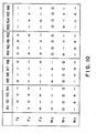
- the bridging portion 214 will expand and the bridging portion 215 will contract. Accordingly, resistance elements (R9 to R12) provided on the bridging portion 214 expand, resulting in an increased electric resistance (in the case of P-type semiconductor), while resistance elements (Rl3 to R16) provided on the bridging portion 215 contract, resulting in a decreased electric resistance. Resistance elements provided on the bridging portions 212 and 213 expand or contract in dependence upon the arrangement positions. Eventually, it will be readily understood that results as shown by the first row in the Table of Fig. 10 are obtained. It will be also understood that results shown by the second to sixth row in the Table of Fig. 10 are obtained.
- bridges as described above, it is possible to cancel the influence of resistance change based on factors except for stress. For example, because electric resistances of respective resistance elements vary in dependence upon temperature, but all resistance elements constituting the bridges vary substantially equally, the influence of such temperature changes is cancelled. Accordingly, such a bridge construction can conduct high accuracy measurement.
- the basic concept of this invention is that resistance elements are arranged in an array as shown in Fig. 7 on the two-dimensional plane, thus to detect three force components and three moment components on the basis of resistance changes due to stress-strains of respective resistance elements.
- the bridging portions formed in the strain generative body 210 may take any form such that strain is produced by force or moment applied to the working point P.
- slits 217 may be provided in respective portions to form bridging portions 212 to 215.
- resistance element elements formed by diffusing impurity on the silicon single crystal substrate were used in the above-described embodiment.
- strain gauges generally used may stack onto one planar surface. From a viewpoint of forming resistance elements on such a planar surface, it is preferable to use semiconductor resistance elements which can be easily manufactured by the semiconductor planar process as in the above-mentioned embodiment.
- the cross sectional view cut along the cutting lines B-B is as shown in Fig. 19.
- a penetration hole 218 in the form of a quadrant when viewed from the upper direction is formed between two adjacent bridging portions.
- thin portion 219 as shown in Fig. 20 between bridging portions without provision of such a penetration hole 218, the advantage with this invention may be obtained.
- the semiconductor substrate has brittle property in general, for actual realization of products, it is desirable to adhere a supporting substrate 223 having rigidity to the strain generative body 210 as shown in Fig. 21.
- resistance elements Rl to R16 which have all the same resistance value in a steady state and produce the same resistance change with respect to the same stress-strain, but it is not necessarily required to use such identical resistance elements.
- components except for diagonal components do not necessarily become equal to "0" in the Table as shown in Fig. 17, resulting in requirement of a predetermined matrix operation. Accordingly, it is preferable for further simplifying an operation for detection to use the same resistance elements as in the above-described embodiment.
- 16 sets of resistance element groups Rl to R16 were formed for detecting three force components and three moment components. However, it is not required to detect all of six components. Where it is sufficient that five components or less can be detected, it is not necessary to form all of 16 sets of resistance element groups, but it is enough to form only resistance element groups at principal positions.
- this detector is constructed to form a plurality of resistance elements at predetermined positions on a planar surface, thus to detect forces in three directions and moments in three directions exerted on the working point on the basis of resistance changes of these resistance elements.
- the detector becomes simplified in structure and computation required for detection becomes simple.
- a method of forming resistance elements used in the detector according to the detector according to this invention is shown.
- a plurality of resistance elements are formed on the semiconductor substrate by the semiconductor planar process.
- an N-type silicon substate 301 is subjected to thermal oxidation to form a silicon oxide layer 302 on the surface thereof.
- the silicon oxide layer 302 is subjected to etching by photo-lithographic method to form openings 303.
- boron is thermally diffused from these openings 303 to form P-type diffused regions 304.
- silicon oxide layers 305 are formed in the'se openings 303.
- silicon nitride is deposited by CVD method to form a silicon nitride layer 306 as a protective layer.
- contact holes are opened in the silicon nitride layer 306 and the silicon oxide layer 305 by photo-lithographic method, thereafter to form an aluminum wiring layer 307 by vacuum deposition as shown in Fig. 22(f).
- patterning is implemented to the aluminum wiring layer 307 by photo-lithographic method, thus to provide a structure as shown in Fig. 22(g).
- the force detector and the moment detector according to this invention can be utilized in a form such that they are embarked or loaded on every industrial machine. Since they are small-sized and low in cost, and permit high accuracy measurement, especially application to automotive vehicles or industrial robots will be expected.
Landscapes
- Physics & Mathematics (AREA)
- General Physics & Mathematics (AREA)
- Force Measurement Appropriate To Specific Purposes (AREA)
Abstract
Description
- This invention relates to a force detector and a moment detector using resistance element, and more particularly to a detector to detect force and moment as stress-strain to convert the stress-strain to a change in resistance value of resistance element, thus to provide an output in the form of an electric signal.
- Generally, a device for detecting force or moment applied on a working point detects stress-strain produced by the application of the force or moment, thereby to indirectly detect force or moment. Detection of stress-strain is made by providing sensors such as strain gauges on respective portions of a strain generative body and producing a stress-strain in response to the application of force or moment to measure changes in, e.g., resistance values, etc. of those sensors. For instance, where a strain gauge is used as the sensor, stress-strain appears in the form of resistance changes of the strain gauge.
- However, the problems with conventional force detector and moment detector are as follows:
- First problem is that the device becomes complicated in structure and becomes large-sized. Namely, since a stress sensor such as a strain gauge must be stuck onto a body which is an object in which a stress-strain is caused (hereinafter such a body is referred to as a strain generative body), it is difficult to allow the device to be small-sized. Particularly, in the case of detecting forces and moments in regard to respective directions of three dimensions, it is required to construct a strain generative body in three dimensions to arrange a plurality of strain gauges in three dimensions, so that the structure of the device becomes extremely complicated.
- Second problem is that such a conventional device is not suitable for mass production and becomes costly. It is very difficult to conduct the above-mentioned work for sticking strain gauges onto a strain generative body of complicated structure in accordance with a manufacturing line having good efficiency.
- Third problem is that measurement accuracy is low. This is because there is a limit in the accuracy of a conventional stress sensor such as a strain gauge, thus failing to make a high precision measurement.
- Fourth problem is that complicated computation is required for detecting a force or moment in a specified direction. For example, in the case of arranging strain gauges in three dimensions to independently detect six quantities of forces exerted or applied in respective axial directions and moments exerted or applied about respective axes on the basis of respective outputs thereof, respectively, a complicated computation is required. Since strain gauges respond to given six quantities, respectively, it is required for measuring a specific quantity to perform such a computation to cancel other five quantities.
- A first object of this invention is to provide a force detector and a moment detector which are simple in structure and can be small-sized.
- A second object of this invention is to provide a force detector and a moment detector which are suitable for mass producibility and can be reduced in the manufacturing cost.
- A third object of this invention is to provide a force detector and a moment detector which are capable of making a high accuracy measurement.
- A fourth object of this invention is to provide a force detector and a moment detector which are capable of obtaining desired measured values with a simple computation.
- This invention has attained the above-described objects by the following features.
- The first feature of this invention resides in that there are provided, in a moment detector, a semiconductor substrate provided on one surface thereof with resistance elements having an electric resistance varying due to mechanical deformation, a working body for applying an angular moment to a working point provided at a point on the semiconductor substrate, and a supporting body for fixedly supporting a portion spaced from the working point of the semiconductor substrate, wherein an opening produces an uneven stress in the semiconductor substrate when an angular moment is applied to the working point is formed in the semiconductor substrate, thus to detect the uneven stress as changes in the electric resistances of the resistance elements.
- In accordance with the above-described moment detector, angular moment is applied to the working point of the semiconductor substrate through the working body. Since a portion of the semiconductor substrate is fixedly supported by the supporting body, a stress is applied to the semiconductor substrate by the applied angular moment. In addition, since an opening is formed in the semiconductor substrate, this stress becomes uneven on the substrate. Accordingly, the resistances of resistance elements formed on the substrate vary in dependence upon the direction and the magnitude of the applied angular moment. Thus, moment can be detected as an electric signal.
- Since resistance elements are all formed on one surface of the semiconductor substrate, the structure becomes very simple. Thus, the detector can be small-sized and becomes suitable for mass production. In addition, since such a resistance element has a sensitivity larger than that of strain gauge, measurement accuracy is improved.
- In a device for detecting forces exerted in respective axial directions and moments exerted around respective axes with an origin being as a working point in an XYZ three-dimensional coordinate system, the second feature of this invention resides in provision of:
- first bridging portions formed along the X-axis on respective both sides of the origin; and
- second bridging portions formed along the Y-axis on respective both sides of the origin,
- wherein both the ends of the first and second bridging portions are fixed as fixed portions so that strains are produced in respective bridging portions by applying a force to the origin, respectively, and
- wherein resistance element groups comprising a plurality of resistance elements having a property such that electric resistance changes due to mechanical deformation are provided on the XY plane of the first and second bridging portions at principal positions of the following positions:
- a pair of positions for resistance elements arranged on both sides of the X-axis in respective positive and negative directions of the Y-axis in the vicinity of the orign in the positive direction of the X-axis,
- a pair of positions for resistance elements arranged on both sides of the X-axis in respective positive and negative directions of the Y-axis in the vicinity of the origin in the negative direction of the X-axis,
- a pair of positions for resistance elements arranged on both sides of the X-axis in respective positive and negative directions of the X-axis in the vicinity of the fixed portion in the positive direction of the X-axis,
- a pair of positions for resistance elements arranged on both sides of the X-axis in respective positive and negative directions of the Y-axis in the vicinity of the fixed portion in the negative direction of the X-axis,
- a pair of positions for resistance elements arranged on both sides of the Y-axis in respective positive and negative directions of the X-axis in the vicinity of the origin in the positive direction of the Y-axis,
- a pair of position for resistance elements arranged on both side of the Y-axis in respective positive and negative directions of the X-axis in the vicinity of the origin in the negative direction of the Y-axis,
- a pair of positions for resistance elements arranged on both side of the Y-axis in respective positive and negative directions of the X-axis in the vicinity of the fixed portion in the positive direction of the Y-axis, and
- a pair of positions for resistance elements arranged on both side of the Y-axis in respective positive and negative directions of the X-axis in the vicinity of the fixed portion in the negative directin of the Y-axis,
- thus to detect changes in the forces acting on the origin on the basis of changes in electric resistances of respective resistance elements.
- In accordance with the above-described detector, resistance elements serving as a sensor for stress-strain are all formed on the XY plane. Accordingly, the device body can be constructed in a planar shape without allowing it to be constructed in three dimensions as in the conventional device. Thus, the device can be realized as a simple configuration.
- In addition, since resistance elements serving as a sensor have a property such that electric resistance varies due to mechanical deformation and respective two resistance elements are paired to arrange them at specified positions, forces in respective axial directions and moments around respective axes can be independently detected by a simple computation.
-
- Figs. 1 and 2 are a top view and a side cross sectional view of a moment detector according to an embodiment of this invention, respectively;
- Fig. 3 is a circuit diagram showing the bridge construction of resistance elements in the device shown in Fig. 1;
- Figs. 4 and 5 are views showing the operational principle of the device shown in Fig. 1;
- Figs. 6 (a) and 6 (b) are views showing a moment detector according to another embodiment of this invention;
- Fig. 7 is a top view of a detector according to an embodiment of this invention;
- Fig. 8 is a cross sectional view cut along the cutting lines A-A of the detector shown in Fig. 7;
- Figs. 9 (a) - 9 (f) are circuit diagrams of six bridges formed with respective resistance elements of the detector shown in Fig. 7;
- Fig. 10 is a Table showing resistance changes of respective resistance elements of the detector shown in Fig. 7;
- Figs. 11 (a) - ll(c) are views showing the state where a force in an X-axis direction is exerted on the device shown in Fig. 7;
- Figs. 12 (a) - 12 (c) are views showing the state where a force in a Y-axis direction is exerted on the device shown in Fig. 7;
- Figs. 13 (a) - 13 (c) are views showing the state where a force in a Z-axis direction is exerted on the device shown in Fig. 7;
- Figs. 14 (a) - 14 (c) views showing the state where a moment around the X-axis is exerted on the device shown in Fig. 7;
- Figs. 15 (a) - 15(c) are views showing the state where a moment around the Y-axis is exerted on the device shown in Fig. 7;
- Figs. 16 (a) - 16 (c) are views showing the state where a moment around the Z-axis is exerted on the device shown in Fig. 7,
- Fig. 17 is a Table showing the relationship between a force to be detected and a voltage detected in the device shown in Fig. 7;
- Fig. 18 is a top view of a detector according to another embodiment of this invention;
- Fig. 19 is a cross sectional view cut along the cutting lines B-B of the device shown in Fig. 7,
- Fig. 20 is a cross sectional view of a detector according to a further embodiment of this invention;
- Fig. 21 is a side view of a detector according to a still further embodiment of this invention; and
- Fig. 22 is a sequential diagram of a process for forming resistance elements used in this invention on a semiconductor substrate.
- Fig. 1 is a top view of a moment detector according to an embodiment of this invention, and Fig. 2 is a side cross sectional view cut along the cutting lines A-A of the above detector. This detector is provided with a silicon
single crystal substrate 110, a workingbody 120 adhered to thecentral portion 111 of thesubstrate 110, and a supportingbody 130 for fixedly supporting theperipheral portion 112 of thesubstrate 110 at a measurement place. Moreover, twoopenings 113 are provided in thesubstrate 110. By providing these-'openings 113, two bridgingportions 114 are formed between thecentral portion 111 and theperipheral portion 112. On the surfaces of these bridgingportions 114, resistance elements rl to r4 and resistance elements rll to rl4 are formed, respectively. Such resistance elements r have a piezo resistance effect such that electric resistance changes due to mechanical deformation, and their structure and the forming method thereof will be described later in detail. - Wiring as shown in Fig. 3 is implemented to respective resistance elements. Namely, a bridge circuit is constructed with resistance elements rl to r4. A voltage is delivered from a
power source 140 to the bridge circuit. The bridge voltage is measured by avoltage meter 150. Although not shown in Fig. 3, also for resistance elements rll to rl4, a bridge cricuit is constructed in a manner similar to the above. - The operation of this detector will be now described with reference to Figs. 4 and 5. Figs. 4 and 5 are views showing stress-strains produced where rotations are applied to the
single crystal substrate 110 counterclockwise when viewed from the upper direction and clockwise when viewed in the same manner, respectively. Around the central points P, angular moments are produced in direction indicated by arrows, respectively. Since theperipheral portion 112 is fixedly supported to the outside, strains will be produced in the bridgingbodies 114. However, sinceopenings 113 are produced in thesubstrate 110, such strains do not become uniform within the substrate, so that strains applied will vary in dependence upon respective resistance elements r. For example, where a strain as shown in Fig. 4 is produced, when the conductivity of each resistance element is assumed to be of P-type, each electric resistance of the resistance elements rl and r4 will increase because a force is applied to them in a direction such that they expand, and each electric resistance of the resistance elements r2 and r3 will decrease because a force is applied to them in a direction such that they contract. In contrast, where strains as shown in Fig. 5 are produced, a phenomenon opposite to the above takes place. - When it is now assumed that resistance elements rl and r4 are called a first pair of resistance elements and resistance elements r2 and r3 are called a second pair of resistance elements, resistance elements r belonging to the same resistance element pairs will make similar changes with respect to an angular moment in a predetermined direction. When an attention is now drawn to the bridge circuit shown in Fig. 3, resistance elements r constituting the same resistance element pairs are positioned at opposite sides, respectively. Accordingly, for an angular moment as shown in Fig. 4, the first pair of resistance elements indicate an increase in resistance, and the second pair of resistance elements indicate a decrease in resistance. In contrast, for an angular moment as shown in Fig. 5, the first pair of resistance elements indicate a decrease in resistance, and the second pair of resistance elements indicate an increase in resistance. Eventually, the polarity of a bridge voltage appearing on the
voltage meter 150 will correspond to the direction of an angular moment around the central point P, and the magnitude of that bridge voltage will correspond to the magnitude of that angular moment. In this way, the direction and the magnitude of an angular moment applied to the workingbody 120 can be detected by the voltage meter l50.. - One merit of the detector according to this embodiment resides in the ability to compensate the influence of resistance changes based on parameters except for stress. The electric resistances of resistance elements r vary also in dependence upon, e.g., temperature, etc. However, as shown in Fig. 1, resistance elements rl and r3 are provided at symmetrical positions and resistance elements r2 and r4 are provided at symmetrical positions, respectively, and thus resistance changes based on parameters except for stress of resistance elements provided at symmetrical positions become equal to each other. Accordingly, resistance changes based on parameters except for stress are cancelled each other, so that such changes do not appear on the output of the
voltage meter 150. - Although only the detection by resistance elements rl to r4 has been described, equivalent results detected may be similarly obtained even with resistance elements rll to r14. By averaging both the results detected, measurement accuracy can be further improved. Alternatively, by selecting a suitable combination of resistance elements from resistance elements rl to r4 and rll to r14, similarly measured results may be obtained. 1.3 Embodiment suitable for realization of products
- The most fundamental embodiment has been described as above. Aside from this, because a semiconductor substrate is generally brittle, it is preferable for actual realization of products to use a rigid body as the working body. Figs. 6 (a) and 6 (b) are views showing such an embodiment wherein Fig. 6(a) is a top view and Fig. 6(b) is a side cross sectional view. In a manner similar to the above-described embodiment,
openings 113 are formed in thesingle crystal substrate 110. Thus, a bridgingportion 114 is formed. On the bridgingportion 114, resistance elements r are formed. Thesingle crystal substrate 110 itself is adhered to a rigidflat plate portion 161 comprised of e.g., metal material and a workingportion 162 connected thereto. Respective resistance elements r are connected towiring terminals 164 throughbonding wires 163. In this case, it is preferable to provide aprotective cover 165 over the device. - By forming the working
portion 162 as a rigid body as stated above, an angular moment to be measured will be transmitted to thesemiconductor substrate 110 through therigid body 161, resulting in an improved durability. 1.4 Advantages with this device - Thus, since the above-described device uses resistance elements formed planar on the single crystal substrate, its structure becomes very simple. Moreover, since manufacturing can be conducted by ordinary semiconductor manufacturing processes, the device is suitable for mass production, can be reduced in cost, and can be small-sized. In addition, since resistance elements are comprised of a single crystal and therefore high accuracy resistance changes due to stress can be obtained, high precision measurement can be carried out.
- Fig. 7 is a top view of a detector according to an embodiment of this invention, and Fig. 8 is a cross sectional view cut along the cutting lines A-A of the detector shown in Fig. 7. In this embodiment, 16 sets of resistance element groups Rl to R16 are formed on the surface of a strain
generative body 210. The straingenerative body 210 is comprised of a silicon single crystal substrate. The resistance element groups Rl to R16 are sets of a plurality of resistance elements, respectively. Respective resistance elements are formed by diffusing impurities on the single crystal substrate. Resistance elements thus formed indicate piezo resistance effect and have a property such that electric resistance varies due to mechanical deformation. - The strain
generative body 210 is composed of an annular fixedportion 211 formed along the periphery thereof, four bridgingportions 212 to 215, and a workingportion 216 to which the four bridgingportions 212 to 215 are coupled. The fixedportion 211 is fixed to the outside and a force or moment to be detected is applied to the working point P positioned in the center of the workingportion 216. Since the fixedportion 211 is fixed to the outside, when a force or a moment is applied to the working point P, strains based on stress corresponding to this force or moment are produced in the bridgingportions 212 to 215. As a result, changes in electric resistance occur in the resistance element groups Rl to R16. This detector serves to detect force and moment on the basis of such changes of electric resistance. In this embodiment, respective resistance elements are the same in dimension, shape and material, and all have a resistance value equal to each other. In addition, resistance change rates based on the stress-strains are all equal to each other. - It is now assumed that, as shown in Figs. 7 and 8, the working point P positioned in the center of the working
portion 216 is set to the origin of the XYZ three-dimensional coordinate system, and three axes of X, Y and Z are defined as shown. Namely, it is assumed that the right direction of Fig. 7, the lower direction thereof, and the direction along the direction perpendicular to the plane of the paper are defined as X-, Y- and Z-axis positive directions, respectively. Workingbodies portion 216. Thus, forces and moments exerted on the working point P will be all applied through the workingbodies move working bodies move working bodies bodies body 221 in an upper direction along the direction perpendicular to the plane of the paper and the workingbody 222 in a lower direction along the direction perpendicular to the plane of the paper. The moment MY around the Y-axis serves as such a moment to move the workingbody 221 in a left direction of the figure and the workingbody 222 in a right direction of the figure. Moreover, the moment MZ around the Z-axis serves as such a moment to both move the workingbodies - The above-mentioned 16 sets of resistance element groups Rl to R16 are arranged at symmetrical positions as shown in Fig. 7. Namely, resistance elements Rl to R4, R5 to R8, R9 to R12, and R13 to R16 are provided at the bridging
portions portion 211 and the workingportion 216, respectively, and respective pairs of resistance element groups are provided on both the sides of the X-axis or Y-axis between which they are put. - By using such 16 sets of resistance element groups, six kinds of bridges as shown in Figs. 9(a) to (f) are formed. To these bridges,
power sources 230 are connected, respectively, andvoltage meters 241 to 246 to output voltages VFX, VFY, VFZ, VMX, VMY, and VMZ proportional to FX, FY, FZ, MX, MY, and MZ are connected, respectively. - It is to be noted that symbols of respective resistance elements shown in this bridge circuit diagram mean one resistance element in the resistance element group, and even if resistance elements are labeled the same symbols, those elements mean other resistance elements belonging to the same resistance element groups. For example, Rl is used in two bridges in Figs. 9(b) and (d). In practice, two resistance elements are arranged at the position of Rl in Fig. 7 and different resistance elements are used in different bridges.
- For convenience of explanation, also for expressing one resistance element belonging to the resistance element group Rx (x = 1 to 16), the same symbol Rx will be used.
- The operation of the above-described device will be described. When forces or moments FX, FY, FZ, MX, MY, and MZ are applied to the working point P in the arrangement of resistance elements as shown in Fig. 7, respective resistance elements Rl to R16 produce electric resistance changes as indicated by the Table shown in Fig. 10 (respective resistance elements are assumed to be comprised of a P-type semiconductor), wherein "0", "+" and "-" indicate no change, an increase in electric resistance, and a decrease in electric resistance, respectively.
- Here, the reason why results as shown in Fig. 10 are obtained will be briefly described with reference to Figs. 11 to 16. Figs. 11 to 16 are views showing stress-strains and changes in electric resistance produced in the bridging portions when forces or moments FX, FY, FZ, MX, MY, and MZ are applied to the working point P, respectively, wherein (a), (b) and (c) are a top view of the bridging portions, a front cross sectional view thereof, and a side cross sectional view thereof in these figures, respectively. For example, the state where the force FX in the X-axis direction is exerted on the working point P is shown in Fig. ll. By the force FX, the bridging
portion 214 will expand and the bridgingportion 215 will contract. Accordingly, resistance elements (R9 to R12) provided on the bridgingportion 214 expand, resulting in an increased electric resistance (in the case of P-type semiconductor), while resistance elements (Rl3 to R16) provided on the bridgingportion 215 contract, resulting in a decreased electric resistance. Resistance elements provided on the bridgingportions - Now, by taking into consideration the fact that bridges as shown in Figs. 9's are constructed by respective resistance elements Rl to R16, the relationship between FX, FY, FZ, MX, MY, and MZ applied to the working point P and voltages detected VFX, VFY, VFZ, VMX, VMY and VMZ appearing on the
voltage meters 241 to 246 is indicated by the Table shown in Fig. 17, wherein "0" indicates that no voltage change is produced and "V" indicates that a voltage change dependent upon an applied force or moment occurs. The polarity of the voltage change depends upon the direction of an applied force or moment, and the magnitude of the voltage change depends upon the magnitude of an applied force or moment. - It will be readily understood that Table as shown in Fig. 17 is obtained when attention.is drawn to the fact that there is no voltage change in the case where products of resistance values of resistance elements provided at respective opposite sides of the bridge are equal to each other in the circuit diagram of Fig. 9. For instance, when force FX is applied, respective resistance elements produce changes in electric resistance as indicated by the first row in the Table of Fig. 10. Referring now to Fig. 9(a), resistance values of R9, R10, Rll and R12 are all increased and resistance values of R13, R14, R15 and R16 are all decreased. Accordingly, there is a great difference between products of resistance values of resistance elements provided at opposite sides. Thus, a voltage change "V" will be detected. On the other hand, there is produced no bridge voltage in the bridge circuits shown in Figs. 9(b) to (f). For instance, in the circuit of Fig. 9(b), if Rl indicates "-", then R2 indicates "+", so that resistance changes are cancelled every branch. As just described above, the action of the force FX is exerted on only VFX, thus making it possible to independently detect the force FX by measurement of VFX.
- The fact that only the diagonal components indicate "V" and components except for the above indicate "0" means that respective values detected can be directly obtained as values read from the voltage meters without performing any computation.
- It is to be noted that by constructing bridges as described above, it is possible to cancel the influence of resistance change based on factors except for stress. For example, because electric resistances of respective resistance elements vary in dependence upon temperature, but all resistance elements constituting the bridges vary substantially equally, the influence of such temperature changes is cancelled. Accordingly, such a bridge construction can conduct high accuracy measurement.
- This invention has been described on the basis of the embodiment illustrated, but this invention is not limited only to such an embodiment. The basic concept of this invention is that resistance elements are arranged in an array as shown in Fig. 7 on the two-dimensional plane, thus to detect three force components and three moment components on the basis of resistance changes due to stress-strains of respective resistance elements. The bridging portions formed in the strain
generative body 210 may take any form such that strain is produced by force or moment applied to the working point P. As shown in Fig. 18, slits 217 may be provided in respective portions to form bridgingportions 212 to 215. - Further, for resistance element, elements formed by diffusing impurity on the silicon single crystal substrate were used in the above-described embodiment. In addition, strain gauges generally used may stack onto one planar surface. From a viewpoint of forming resistance elements on such a planar surface, it is preferable to use semiconductor resistance elements which can be easily manufactured by the semiconductor planar process as in the above-mentioned embodiment.
- In the above-described embodiment shown in Fig. 7, the cross sectional view cut along the cutting lines B-B is as shown in Fig. 19. Namely, a
penetration hole 218 in the form of a quadrant when viewed from the upper direction is formed between two adjacent bridging portions. In addition, by providingthin portion 219 as shown in Fig. 20 between bridging portions without provision of such apenetration hole 218, the advantage with this invention may be obtained. - Moreover, since the semiconductor substrate has brittle property in general, for actual realization of products, it is desirable to adhere a supporting
substrate 223 having rigidity to the straingenerative body 210 as shown in Fig. 21. - In the above-described embodiment, there were used resistance elements Rl to R16 which have all the same resistance value in a steady state and produce the same resistance change with respect to the same stress-strain, but it is not necessarily required to use such identical resistance elements. In this case, components except for diagonal components do not necessarily become equal to "0" in the Table as shown in Fig. 17, resulting in requirement of a predetermined matrix operation. Accordingly, it is preferable for further simplifying an operation for detection to use the same resistance elements as in the above-described embodiment.
- In the above-described embodiment, 16 sets of resistance element groups Rl to R16 were formed for detecting three force components and three moment components. However, it is not required to detect all of six components. Where it is sufficient that five components or less can be detected, it is not necessary to form all of 16 sets of resistance element groups, but it is enough to form only resistance element groups at principal positions.
- As described above, this detector is constructed to form a plurality of resistance elements at predetermined positions on a planar surface, thus to detect forces in three directions and moments in three directions exerted on the working point on the basis of resistance changes of these resistance elements. Thus, the detector becomes simplified in structure and computation required for detection becomes simple.
- Finally, an example of a method of forming resistance elements used in the detector according to the detector according to this invention is shown. On the semiconductor substrate, a plurality of resistance elements are formed. These resistance elements have piezo resistance effect and are formed on the semiconductor substrate by the semiconductor planar process. First, as shown in Fig. 22(a), an N-
type silicon substate 301 is subjected to thermal oxidation to form asilicon oxide layer 302 on the surface thereof. Then, as shown in Fig. 22(b), thesilicon oxide layer 302 is subjected to etching by photo-lithographic method to formopenings 303. Subsequently, as shown in Fig. 22(c), boron is thermally diffused from theseopenings 303 to form P-type diffusedregions 304. It is to be noted thatsilicon oxide layers 305 are formed inthe'se openings 303. Then, as shown in Fig. 22(d), silicon nitride is deposited by CVD method to form asilicon nitride layer 306 as a protective layer. Further, as shown in Fig. 22(e), contact holes are opened in thesilicon nitride layer 306 and thesilicon oxide layer 305 by photo-lithographic method, thereafter to form analuminum wiring layer 307 by vacuum deposition as shown in Fig. 22(f). Finally, patterning is implemented to thealuminum wiring layer 307 by photo-lithographic method, thus to provide a structure as shown in Fig. 22(g). - It is to be noted that the above-described manufacturing process is illustrated as only one example, and therefore this invention may be realized in principle even with any resistance element such that electric resistance varies due to mechanical deformation.
- The force detector and the moment detector according to this invention can be utilized in a form such that they are embarked or loaded on every industrial machine. Since they are small-sized and low in cost, and permit high accuracy measurement, especially application to automotive vehicles or industrial robots will be expected.
Claims (8)
Applications Claiming Priority (5)
| Application Number | Priority Date | Filing Date | Title |
|---|---|---|---|
| JP62101268A JPS63266324A (en) | 1987-04-24 | 1987-04-24 | Moment detector |
| JP101268/87 | 1987-04-24 | ||
| JP101272/87 | 1987-04-24 | ||
| JP62101272A JPS63266329A (en) | 1987-04-24 | 1987-04-24 | Force detector |
| PCT/JP1988/000394 WO1988008521A1 (en) | 1987-04-24 | 1988-04-22 | Force and moment detector using resistor |
Publications (3)
| Publication Number | Publication Date |
|---|---|
| EP0311695A1 true EP0311695A1 (en) | 1989-04-19 |
| EP0311695A4 EP0311695A4 (en) | 1991-10-02 |
| EP0311695B1 EP0311695B1 (en) | 1994-11-30 |
Family
ID=26442171
Family Applications (1)
| Application Number | Title | Priority Date | Filing Date |
|---|---|---|---|
| EP88903392A Expired - Lifetime EP0311695B1 (en) | 1987-04-24 | 1988-04-22 | Force and moment detector using resistor |
Country Status (4)
| Country | Link |
|---|---|
| US (2) | US4905523A (en) |
| EP (1) | EP0311695B1 (en) |
| DE (1) | DE3852271T2 (en) |
| WO (1) | WO1988008521A1 (en) |
Cited By (2)
| Publication number | Priority date | Publication date | Assignee | Title |
|---|---|---|---|---|
| EP0381187A3 (en) * | 1989-02-01 | 1992-03-25 | Wacoh Corporation | Force detector using resistance elements |
| US11035746B2 (en) | 2018-12-20 | 2021-06-15 | Industrial Technology Research Institute | Multi-axis force sensor capable of reducing influence on the other when measuring one of the axial force and torque |
Families Citing this family (71)
| Publication number | Priority date | Publication date | Assignee | Title |
|---|---|---|---|---|
| US6864677B1 (en) * | 1993-12-15 | 2005-03-08 | Kazuhiro Okada | Method of testing a sensor |
| WO1991010118A1 (en) | 1989-12-28 | 1991-07-11 | Wacoh Corporation | Apparatus for detecting physical quantity that acts as external force and method of testing and producing this apparatus |
| US5421213A (en) | 1990-10-12 | 1995-06-06 | Okada; Kazuhiro | Multi-dimensional force detector |
| US6314823B1 (en) * | 1991-09-20 | 2001-11-13 | Kazuhiro Okada | Force detector and acceleration detector and method of manufacturing the same |
| JP3141954B2 (en) * | 1991-07-17 | 2001-03-07 | 株式会社ワコー | Force / acceleration / magnetism sensors using piezoelectric elements |
| JP3027457B2 (en) * | 1991-10-25 | 2000-04-04 | 和廣 岡田 | Force, acceleration, and magnetism detectors for multi-dimensional directions |
| EP0540094A1 (en) * | 1991-10-30 | 1993-05-05 | Laboratoires D'electronique Philips S.A.S. | Multidirectional control device |
| US6282956B1 (en) * | 1994-12-29 | 2001-09-04 | Kazuhiro Okada | Multi-axial angular velocity sensor |
| US5646346A (en) * | 1994-11-10 | 1997-07-08 | Okada; Kazuhiro | Multi-axial angular velocity sensor |
| JP3256346B2 (en) * | 1993-07-29 | 2002-02-12 | 和廣 岡田 | Force / acceleration / magnetism sensors using piezoelectric elements |
| JP3549590B2 (en) * | 1994-09-28 | 2004-08-04 | 和廣 岡田 | Acceleration / angular velocity sensor |
| US6003371A (en) | 1995-02-21 | 1999-12-21 | Wacoh Corporation | Angular velocity sensor |
| JP3585980B2 (en) * | 1995-02-21 | 2004-11-10 | 株式会社ワコー | Angular velocity sensor |
| JPH0949856A (en) * | 1995-05-31 | 1997-02-18 | Wako:Kk | Acceleration sensor |
| JPH09119943A (en) * | 1995-10-24 | 1997-05-06 | Wako:Kk | Acceleration sensor |
| DE19627385A1 (en) * | 1996-07-06 | 1998-01-08 | Bayerische Motoren Werke Ag | Wheel hub |
| JP4011626B2 (en) * | 1996-07-10 | 2007-11-21 | 株式会社ワコー | Angular velocity sensor |
| US6367326B1 (en) | 1996-07-10 | 2002-04-09 | Wacoh Corporation | Angular velocity sensor |
| US5966117A (en) | 1996-11-25 | 1999-10-12 | Cts Corporation | Z-axis sensing pointing stick with base as strain concentrator |
| US20020018048A1 (en) * | 1997-02-04 | 2002-02-14 | Seffernick Lewis L. | Z-axis pointing stick with esd protection |
| JP4176849B2 (en) * | 1997-05-08 | 2008-11-05 | 株式会社ワコー | Sensor manufacturing method |
| US6121954A (en) * | 1997-09-26 | 2000-09-19 | Cts Corporation | Unified bodied z-axis sensing pointing stick |
| US6239786B1 (en) | 1998-11-30 | 2001-05-29 | Cts Corporation | Pointing stick with top mounted z-axis sensor |
| US6331849B1 (en) | 1999-02-25 | 2001-12-18 | Cts Corporation | Integrated surface-mount pointing device |
| US6323840B1 (en) | 1999-09-17 | 2001-11-27 | Cts Corporation | Surface-mount pointing device |
| JP4295883B2 (en) | 1999-12-13 | 2009-07-15 | 株式会社ワコー | Force detection device |
| DE10037782A1 (en) * | 2000-08-03 | 2002-02-14 | Hbm Mes Und Systemtechnik Gmbh | Torque sensor for e.g. drive shaft of motor vehicle, has torque introduction element provided on transverse middle plane between measurement springs, in longitudinal direction of double flexional-bar |
| US6970159B2 (en) | 2001-06-25 | 2005-11-29 | Gray Robin S | Mouse printing device with integrated touch pad buttons |
| US6809529B2 (en) | 2001-08-10 | 2004-10-26 | Wacoh Corporation | Force detector |
| JP4216525B2 (en) * | 2002-05-13 | 2009-01-28 | 株式会社ワコー | Acceleration sensor and manufacturing method thereof |
| JP4125931B2 (en) * | 2002-08-26 | 2008-07-30 | 株式会社ワコー | Rotation operation amount input device and operation device using the same |
| JP4271475B2 (en) * | 2003-03-31 | 2009-06-03 | 株式会社ワコー | Force detection device |
| JP4907050B2 (en) * | 2003-03-31 | 2012-03-28 | 株式会社ワコー | Force detection device |
| JP4387691B2 (en) * | 2003-04-28 | 2009-12-16 | 株式会社ワコー | Force detection device |
| ITMI20031500A1 (en) * | 2003-07-22 | 2005-01-23 | Milano Politecnico | DEVICE AND METHOD FOR THE MEASUREMENT OF FORCES AND MOMENTS |
| US20060049001A1 (en) * | 2004-09-09 | 2006-03-09 | Mark Streitman | Driven pendulum apparatus and method of operation thereof |
| JP4680566B2 (en) * | 2004-10-26 | 2011-05-11 | 本田技研工業株式会社 | Multi-axis force sensor chip and multi-axis force sensor using the same |
| US7337671B2 (en) | 2005-06-03 | 2008-03-04 | Georgia Tech Research Corp. | Capacitive microaccelerometers and fabrication methods |
| JP4203051B2 (en) * | 2005-06-28 | 2008-12-24 | 本田技研工業株式会社 | Force sensor |
| US7284444B2 (en) * | 2005-12-30 | 2007-10-23 | Kulite Semiconductor Products, Inc. | Hermetically sealed displacement sensor apparatus |
| US7578189B1 (en) * | 2006-05-10 | 2009-08-25 | Qualtre, Inc. | Three-axis accelerometers |
| JP5243704B2 (en) * | 2006-08-24 | 2013-07-24 | 本田技研工業株式会社 | Force sensor |
| JP2008058110A (en) * | 2006-08-30 | 2008-03-13 | Honda Motor Co Ltd | Force sensor chip and force sensor |
| JP5174343B2 (en) * | 2006-12-12 | 2013-04-03 | 本田技研工業株式会社 | Force sensor chip |
| JP2008190931A (en) * | 2007-02-02 | 2008-08-21 | Wacoh Corp | Sensor that detects both acceleration and angular velocity |
| JP5243988B2 (en) * | 2009-02-10 | 2013-07-24 | 本田技研工業株式会社 | Multi-axis force sensor and acceleration sensor |
| JP5439068B2 (en) * | 2009-07-08 | 2014-03-12 | 株式会社ワコー | Force detection device |
| EP2426083A3 (en) | 2010-09-03 | 2013-11-13 | Domintech Co., LTD. | Mems sensor package |
| TWI414478B (en) | 2010-09-09 | 2013-11-11 | Domintech Co Ltd | Mems sensor capable of measuring acceleration and pressure |
| US9323010B2 (en) | 2012-01-10 | 2016-04-26 | Invensas Corporation | Structures formed using monocrystalline silicon and/or other materials for optical and other applications |
| US8757897B2 (en) | 2012-01-10 | 2014-06-24 | Invensas Corporation | Optical interposer |
| US10273147B2 (en) | 2013-07-08 | 2019-04-30 | Motion Engine Inc. | MEMS components and method of wafer-level manufacturing thereof |
| JP6339669B2 (en) | 2013-07-08 | 2018-06-06 | モーション・エンジン・インコーポレーテッド | MEMS device and method of manufacturing |
| WO2015013827A1 (en) | 2013-08-02 | 2015-02-05 | Motion Engine Inc. | Mems motion sensor for sub-resonance angular rate sensing |
| JP5529328B1 (en) | 2013-09-04 | 2014-06-25 | 株式会社トライフォース・マネジメント | Power generation element |
| CN103575446B (en) * | 2013-10-11 | 2016-04-27 | 南京神源生智能科技有限公司 | A kind of Medium-measurement-rthree-dimensional three-dimensional force sensor |
| WO2015103688A1 (en) | 2014-01-09 | 2015-07-16 | Motion Engine Inc. | Integrated mems system |
| US20170030788A1 (en) | 2014-04-10 | 2017-02-02 | Motion Engine Inc. | Mems pressure sensor |
| US11674803B2 (en) | 2014-06-02 | 2023-06-13 | Motion Engine, Inc. | Multi-mass MEMS motion sensor |
| US11287486B2 (en) | 2014-12-09 | 2022-03-29 | Motion Engine, Inc. | 3D MEMS magnetometer and associated methods |
| US10407299B2 (en) | 2015-01-15 | 2019-09-10 | Motion Engine Inc. | 3D MEMS device with hermetic cavity |
| US10416030B2 (en) | 2015-01-26 | 2019-09-17 | Wacoh-Tech Inc. | Force sensor |
| JP6002868B1 (en) | 2015-04-07 | 2016-10-05 | 株式会社トライフォース・マネジメント | Force sensor and structure used therefor |
| JP5996078B1 (en) | 2015-10-19 | 2016-09-21 | 株式会社トライフォース・マネジメント | Power generation element |
| US10422707B2 (en) * | 2016-01-19 | 2019-09-24 | Ati Industrial Automation, Inc. | Compact robotic force/torque sensor including strain gages |
| US10067019B2 (en) | 2016-01-25 | 2018-09-04 | Ati Industrial Automation, Inc. | Force and torque sensor having redundant instrumentation and operative to detect faults |
| TW201728905A (en) * | 2016-02-03 | 2017-08-16 | 智動全球股份有限公司 | Accelerometer |
| CN106323524B (en) * | 2016-08-19 | 2021-10-26 | 国网河南省电力公司电力科学研究院 | System and method for measuring static tension of straight-line-shaped hardware fitting at end part of high-voltage sleeve of transformer |
| US10352792B2 (en) * | 2017-02-15 | 2019-07-16 | Texas Instruments Incorporated | Device and method for on-chip mechanical stress sensing |
| JP6964212B2 (en) * | 2019-07-24 | 2021-11-10 | Semitec株式会社 | A device equipped with a contact force sensor and a contact force sensor |
| US11892364B2 (en) | 2022-02-10 | 2024-02-06 | Ati Industrial Automation, Inc. | Torque sensor using coupled loads and fewer strain gages |
Family Cites Families (8)
| Publication number | Priority date | Publication date | Assignee | Title |
|---|---|---|---|---|
| US3620073A (en) * | 1968-09-18 | 1971-11-16 | Honeywell Inc | Control wheel force steering apparatus |
| JPS5780532A (en) * | 1980-11-07 | 1982-05-20 | Hitachi Ltd | Semiconductor load converter |
| US4373399A (en) * | 1981-02-05 | 1983-02-15 | Beloglazov Alexei V | Semiconductor strain gauge transducer |
| JPS57169643A (en) * | 1981-04-13 | 1982-10-19 | Yamato Scale Co Ltd | Load cell for multiple components of force |
| US4573362A (en) * | 1984-07-09 | 1986-03-04 | Eaton Corporation | Multi-axis load transducer |
| CA1259816A (en) * | 1984-09-29 | 1989-09-26 | Kazuo Asakawa | Force-detecting apparatus |
| JPS61223626A (en) * | 1985-03-29 | 1986-10-04 | Nec Corp | Sensor |
| JPS61223623A (en) * | 1985-03-29 | 1986-10-04 | Yokogawa Electric Corp | Multipoint temperature measuring device |
-
1988
- 1988-04-22 DE DE3852271T patent/DE3852271T2/en not_active Expired - Fee Related
- 1988-04-22 WO PCT/JP1988/000394 patent/WO1988008521A1/en not_active Ceased
- 1988-04-22 EP EP88903392A patent/EP0311695B1/en not_active Expired - Lifetime
- 1988-04-22 US US07/295,601 patent/US4905523A/en not_active Expired - Fee Related
-
1989
- 1989-11-07 US US07/432,796 patent/US4969366A/en not_active Expired - Fee Related
Cited By (2)
| Publication number | Priority date | Publication date | Assignee | Title |
|---|---|---|---|---|
| EP0381187A3 (en) * | 1989-02-01 | 1992-03-25 | Wacoh Corporation | Force detector using resistance elements |
| US11035746B2 (en) | 2018-12-20 | 2021-06-15 | Industrial Technology Research Institute | Multi-axis force sensor capable of reducing influence on the other when measuring one of the axial force and torque |
Also Published As
| Publication number | Publication date |
|---|---|
| WO1988008521A1 (en) | 1988-11-03 |
| DE3852271D1 (en) | 1995-01-12 |
| DE3852271T2 (en) | 1995-07-06 |
| EP0311695B1 (en) | 1994-11-30 |
| US4969366A (en) | 1990-11-13 |
| US4905523A (en) | 1990-03-06 |
| EP0311695A4 (en) | 1991-10-02 |
Similar Documents
| Publication | Publication Date | Title |
|---|---|---|
| EP0311695B1 (en) | Force and moment detector using resistor | |
| EP0333872B1 (en) | Gripper for a robot | |
| US5263375A (en) | Contact detector using resistance elements and its application | |
| US6185814B1 (en) | Method of manufacturing a sensor detecting a physical action as an applied force | |
| US5182515A (en) | Detector for magnetism using a resistance element | |
| US4967605A (en) | Detector for force and acceleration using resistance element | |
| US5035148A (en) | Force detector using resistance elements | |
| US7578162B2 (en) | Apparatus for detecting a physical quantity acting as an external force and method for testing and manufacturing this apparatus | |
| US5083466A (en) | Multidimensional force sensor | |
| US5526700A (en) | Six component force gage | |
| US7490524B2 (en) | Force sensor chip | |
| EP0195232B1 (en) | Piezoresistive strain sensing device | |
| EP2510325A2 (en) | Multiaxial force-torque sensors | |
| CN100565146C (en) | A flat piezoelectric six-dimensional force sensor | |
| CN119197856A (en) | Six-dimensional force sensor based on planar semiconductor technology and preparation method thereof | |
| CN119984615A (en) | Multi-dimensional force sensor and processing method | |
| JP2663144B2 (en) | Robot gripper | |
| JPH0617834B2 (en) | Force detector | |
| JPH0821721B2 (en) | Force detection device | |
| US4884051A (en) | Semiconductor diffusion type force sensing apparatus | |
| JP2596759B2 (en) | Force detection device | |
| JPH0652269B2 (en) | Acceleration detection device | |
| JPH0793445B2 (en) | Pressure sensor | |
| PL93088B2 (en) | ||
| JPS60153173A (en) | Sense of contact force sensor |
Legal Events
| Date | Code | Title | Description |
|---|---|---|---|
| PUAI | Public reference made under article 153(3) epc to a published international application that has entered the european phase |
Free format text: ORIGINAL CODE: 0009012 |
|
| 17P | Request for examination filed |
Effective date: 19881230 |
|
| AK | Designated contracting states |
Kind code of ref document: A1 Designated state(s): DE FR GB IT |
|
| RAP1 | Party data changed (applicant data changed or rights of an application transferred) |
Owner name: DAI-ICHI SEIKO CO. LTD. |
|
| RAP1 | Party data changed (applicant data changed or rights of an application transferred) |
Owner name: DAI-ICHI SEIKO LABORATORIES, INC. |
|
| A4 | Supplementary search report drawn up and despatched |
Effective date: 19910812 |
|
| AK | Designated contracting states |
Kind code of ref document: A4 Designated state(s): DE FR GB IT |
|
| 17Q | First examination report despatched |
Effective date: 19920724 |
|
| RAP3 | Party data changed (applicant data changed or rights of an application transferred) |
Owner name: ENPLAS LABORATORIES, INC. |
|
| GRAA | (expected) grant |
Free format text: ORIGINAL CODE: 0009210 |
|
| AK | Designated contracting states |
Kind code of ref document: B1 Designated state(s): DE FR GB IT |
|
| REF | Corresponds to: |
Ref document number: 3852271 Country of ref document: DE Date of ref document: 19950112 |
|
| ITF | It: translation for a ep patent filed | ||
| ET | Fr: translation filed | ||
| PLBE | No opposition filed within time limit |
Free format text: ORIGINAL CODE: 0009261 |
|
| STAA | Information on the status of an ep patent application or granted ep patent |
Free format text: STATUS: NO OPPOSITION FILED WITHIN TIME LIMIT |
|
| 26N | No opposition filed | ||
| PGFP | Annual fee paid to national office [announced via postgrant information from national office to epo] |
Ref country code: GB Payment date: 19960319 Year of fee payment: 9 |
|
| PGFP | Annual fee paid to national office [announced via postgrant information from national office to epo] |
Ref country code: FR Payment date: 19960329 Year of fee payment: 9 |
|
| PGFP | Annual fee paid to national office [announced via postgrant information from national office to epo] |
Ref country code: DE Payment date: 19960627 Year of fee payment: 9 |
|
| PG25 | Lapsed in a contracting state [announced via postgrant information from national office to epo] |
Ref country code: GB Effective date: 19970422 |
|
| GBPC | Gb: european patent ceased through non-payment of renewal fee |
Effective date: 19970422 |
|
| PG25 | Lapsed in a contracting state [announced via postgrant information from national office to epo] |
Ref country code: FR Free format text: LAPSE BECAUSE OF NON-PAYMENT OF DUE FEES Effective date: 19971231 |
|
| PG25 | Lapsed in a contracting state [announced via postgrant information from national office to epo] |
Ref country code: DE Free format text: LAPSE BECAUSE OF NON-PAYMENT OF DUE FEES Effective date: 19980101 |
|
| REG | Reference to a national code |
Ref country code: FR Ref legal event code: ST |
|
| PG25 | Lapsed in a contracting state [announced via postgrant information from national office to epo] |
Ref country code: IT Free format text: LAPSE BECAUSE OF NON-PAYMENT OF DUE FEES;WARNING: LAPSES OF ITALIAN PATENTS WITH EFFECTIVE DATE BEFORE 2007 MAY HAVE OCCURRED AT ANY TIME BEFORE 2007. THE CORRECT EFFECTIVE DATE MAY BE DIFFERENT FROM THE ONE RECORDED. Effective date: 20050422 |