EP0055136A2 - A semiconductor buffer circuit - Google Patents
A semiconductor buffer circuit Download PDFInfo
- Publication number
- EP0055136A2 EP0055136A2 EP81306074A EP81306074A EP0055136A2 EP 0055136 A2 EP0055136 A2 EP 0055136A2 EP 81306074 A EP81306074 A EP 81306074A EP 81306074 A EP81306074 A EP 81306074A EP 0055136 A2 EP0055136 A2 EP 0055136A2
- Authority
- EP
- European Patent Office
- Prior art keywords
- circuit
- clock signal
- transistor
- voltage
- output
- Prior art date
- Legal status (The legal status is an assumption and is not a legal conclusion. Google has not performed a legal analysis and makes no representation as to the accuracy of the status listed.)
- Granted
Links
Images


Classifications
-
- H—ELECTRICITY
- H03—ELECTRONIC CIRCUITRY
- H03K—PULSE TECHNIQUE
- H03K19/00—Logic circuits, i.e. having at least two inputs acting on one output; Inverting circuits
- H03K19/01—Modifications for accelerating switching
- H03K19/017—Modifications for accelerating switching in field-effect transistor circuits
- H03K19/01707—Modifications for accelerating switching in field-effect transistor circuits in asynchronous circuits
- H03K19/01714—Modifications for accelerating switching in field-effect transistor circuits in asynchronous circuits by bootstrapping, i.e. by positive feed-back
-
- G—PHYSICS
- G11—INFORMATION STORAGE
- G11C—STATIC STORES
- G11C11/00—Digital stores characterised by the use of particular electric or magnetic storage elements; Storage elements therefor
- G11C11/21—Digital stores characterised by the use of particular electric or magnetic storage elements; Storage elements therefor using electric elements
- G11C11/34—Digital stores characterised by the use of particular electric or magnetic storage elements; Storage elements therefor using electric elements using semiconductor devices
- G11C11/40—Digital stores characterised by the use of particular electric or magnetic storage elements; Storage elements therefor using electric elements using semiconductor devices using transistors
- G11C11/401—Digital stores characterised by the use of particular electric or magnetic storage elements; Storage elements therefor using electric elements using semiconductor devices using transistors forming cells needing refreshing or charge regeneration, i.e. dynamic cells
- G11C11/4063—Auxiliary circuits, e.g. for addressing, decoding, driving, writing, sensing or timing
- G11C11/407—Auxiliary circuits, e.g. for addressing, decoding, driving, writing, sensing or timing for memory cells of the field-effect type
- G11C11/408—Address circuits
-
- G—PHYSICS
- G11—INFORMATION STORAGE
- G11C—STATIC STORES
- G11C11/00—Digital stores characterised by the use of particular electric or magnetic storage elements; Storage elements therefor
- G11C11/21—Digital stores characterised by the use of particular electric or magnetic storage elements; Storage elements therefor using electric elements
- G11C11/34—Digital stores characterised by the use of particular electric or magnetic storage elements; Storage elements therefor using electric elements using semiconductor devices
- G11C11/40—Digital stores characterised by the use of particular electric or magnetic storage elements; Storage elements therefor using electric elements using semiconductor devices using transistors
- G11C11/401—Digital stores characterised by the use of particular electric or magnetic storage elements; Storage elements therefor using electric elements using semiconductor devices using transistors forming cells needing refreshing or charge regeneration, i.e. dynamic cells
- G11C11/4063—Auxiliary circuits, e.g. for addressing, decoding, driving, writing, sensing or timing
- G11C11/407—Auxiliary circuits, e.g. for addressing, decoding, driving, writing, sensing or timing for memory cells of the field-effect type
- G11C11/408—Address circuits
- G11C11/4085—Word line control circuits, e.g. word line drivers, - boosters, - pull-up, - pull-down, - precharge
-
- H—ELECTRICITY
- H03—ELECTRONIC CIRCUITRY
- H03K—PULSE TECHNIQUE
- H03K19/00—Logic circuits, i.e. having at least two inputs acting on one output; Inverting circuits
- H03K19/01—Modifications for accelerating switching
- H03K19/017—Modifications for accelerating switching in field-effect transistor circuits
- H03K19/01728—Modifications for accelerating switching in field-effect transistor circuits in synchronous circuits, i.e. by using clock signals
-
- H—ELECTRICITY
- H03—ELECTRONIC CIRCUITRY
- H03K—PULSE TECHNIQUE
- H03K19/00—Logic circuits, i.e. having at least two inputs acting on one output; Inverting circuits
- H03K19/0175—Coupling arrangements; Interface arrangements
- H03K19/0185—Coupling arrangements; Interface arrangements using field effect transistors only
- H03K19/018507—Interface arrangements
- H03K19/01855—Interface arrangements synchronous, i.e. using clock signals
-
- H—ELECTRICITY
- H03—ELECTRONIC CIRCUITRY
- H03K—PULSE TECHNIQUE
- H03K5/00—Manipulating of pulses not covered by one of the other main groups of this subclass
- H03K5/01—Shaping pulses
- H03K5/02—Shaping pulses by amplifying
- H03K5/023—Shaping pulses by amplifying using field effect transistors
Definitions
- the present invention relates, for example, to a semiconductor circuit used as a buffer circuit having the function of compensating for a power source fluctuation and used for the amplification of a clock signal in a dynamic memory device.
- a conventional buffer circuit which amplifies an input clock signal $ 0 (conversion of impedance) and supplies an output clock signal ⁇ 1 is constituted of MOS transistors Q1 through Q12 (Q9 is a MOS capacitor), as shown in Fig. 1.
- the input stage of the buffer circuit is a delay circuit constituted of transistors Ql through Q4. During a standby period, the delay circuit holds the voltage of the node N2, which connects the source of transistor Q3 with the drain of transistor Q4, at a high level. This is possible because of the input clock signal $ 0 and the inverted input clock signal 0.
- the clock signal ⁇ 0 is at a high level during an active period and is at a low level during the standby period.
- the clock signal ⁇ 0 because of the inverted polarity, is at a low level during the active period and is at a high level during the standby period.
- These clock signals turn off the transistor Ql, turn on the transistors Q2 and Q3, hold the node N1 at a low level, which node N1 connects the source of the transistor Q1 with the drain of the transistor Q2 and the gate of the transistor Q4, turn off the transistor Q4, and charge the node N2 to the voltage of (Vcc-Vth) through the transistor Q3 during the standby period.
- the Vcc is the voltage on the high voltage side of the power source and is usually 5 volts, which is the standard value allowing for an error of ⁇ 10%.
- the Vth is a threshold value of the transistor.
- the gate of the transistor Q5 is connected to the power source Vcc, when the node N2 is charged to the ( V cc-Vth) the node N3 is charged to the same voltage.
- the node N3, which connects the transistor Q5 with the gate of transistor Q6, is the gate terminal of the transistor Q6 in the bootstrap circuit including the transistors Q6 and Q7.
- the transistor Q7 Since the clock signal ⁇ is at a high level during the standby period, the transistor Q7 turns on, the node N4 which connects the source of transistor Q6 with the drain of the transistor Q7, the MOS capacitor Q9, and the gate of transistor Qll reaches a low level, the transistors Q8 and Qll turn off, the transistors Q10 and Q12 turn on, and the output clock signal $ 1 is at a low level which is equal to the low voltage side of the power source Vss (usually ground voltage).
- the input clock signals ⁇ 0 and 0 are inverted.
- waveforms are shown during the active period.
- This example shows a constant Vcc which is equal to 4.5 volts.
- the voltage of the node N2 is equal to the voltage of the node N3 (4.5 volts-Vth) at the end of the standby period
- the clock signal 0 changes from Vcc to Vss
- the clock signal $ 0 changes from Vss to Vcc
- the voltage of the node N3 increases to more than (Vcc + Vth) and the voltage of the node N4 is charged to the voltage of ⁇ 0 , which is equal to Vcc, by means of the bootstrap effect, which is due to the effects of the capacity between the gate and the drain of the transistor Q6 and between the gate and the source of the transistor Q6.
- the transistors Q8 and Qll being turned on.
- the transistor Ql since the transistor Ql turns on, the transistor Q2 turns off, and the node N1 is charged to a voltage of Vcc; then the transistor Q4 turns on and the voltage of the node N2 begins to decrease. Accordingly, the electric charges at the node N3 are attracted by the voltage of node N2 through the transistor Q5 and the voltage of the nodes N3 and N2 decreases to Vss.
- the transistors Q10 and Q12 turn off and the voltage of the node N5 increases to Vcc.
- the transistor Q6 turns off and the voltage of the node N4 is increased to more than (Vcc + Vth) through the capacitor Q9, the output clock signal ⁇ 1 increases to the maximum power source voltage level Vcc.
- the above-mentioned operation is carried out when no fluctuation of the power source occurs.
- the output clock signal $ 1 is delayed, and delay of the output clock signal ⁇ 1 signifies a problem.
- Fig. 3 an example is shown in which the Vcc decreases from 5.5 volts (Vcc(U)) to 4.5 volts (Vcc(L)) during the standby period.
- the above-mentioned fluctuation occurs when the electrical constitution of the constant voltage power supply is simplified in order to reduce the cost of the device or when other devices connected to the same power source are operated.
- the voltage of the clock signal $ 0 is low, the voltage of the clock signal 0 is high and the voltage of Vcc is the upper limit Vcc(U), which is equal to 5.5 volts, causing both the nodes N2 and N3 to be charged to (5.5 volts-Vth). Further, if the Vcc decreases to the lower limit Vcc(L) which is equal to 4.5 volts, during the standby period, the voltage of the nodes N2 and N3 (5.5 volts-Vth) does not change because there is no discharge path.
- the reason there is no discharge path is that the transistor Q4 is in the "off" state, and the gate of the transistor Q3 has a low voltage of 4.5 volts which is equal to ⁇ 0 and Vcc.
- the clock signal ⁇ 1 is delayed.
- the waveforms indicated by the broken lines N2', N3', N5' and ⁇ 1' show the passages of the voltage changes at the nodes N2, N3 and N5 and the voltage of the clock signal ⁇ 1 without a power source fluctuation, as compared with the lines N2, N3, N5 and ⁇ 1 which show the passages of the voltage changes at the nodes N2, N3 and N5 when fluctuation occurs in the power supply.
- the present invention is proposed in order to reduce the above-mentioned problems.
- An embodiment of the present invention can provide a semiconductor circuit used as a buffer circuit in which the voltage of the charged nodes during the standby period corresponds to the voltage of the power source throughout the standby period, thereby improving the delay in the output clock signal caused by fluctuation of the voltage of the power supply and accomplishing high speed access time in a dynamic memory device.
- a semiconductor circuit used as a buffer circuit comprising an input stage circuit for receiving an input clock signal and an inverted input clock signal, a bootstrap circuit, comprising a transistor, for receiving the output of said input stage circuit and for maintaining the gate voltage of said transistor at a high level during a standby period, and an output circuit comprising a transistoi, which is switched on and off by the output of said bootstrap circuit and said input stage circuit, for generating an output clock signal
- said semiconductor circuit further comprising a means by which a high level clock signal, having the same phase as said inverted clock signal and a level higher than the level of the sum of a power source voltage and a transistor threshold voltage, is applied to a gate of a predetermined transistor, whereby the voltage of a point charged during the standby period corresponds to the voltage of the power source throughout the standby period.
- a semiconductor circuit used as a buffer circuit comprising an input stage delay circuit for receiving an input clock signal and an inverted input clock signal, a bootstrap circuit for receiving the output of said input stage delay circuit, said bootstrap circuit increasing the voltage of an output by means of a bootstrap operation, and an output circuit for receiving the output of said bootstrap circuit and said input stage delay circuit and for generating an output clock signal, said semiconductor circuit further comprising a means by which a high level clock signal, having the same phase as said inverted clock signal and a level higher than the level of the sum of a power source voltage and a transistor threshold voltage, is applied to a gate of a transistor for connecting a first node connecting the output of said input stage delay circuit with the input of said bootstrap circuit with one of the output terminals of the power source, whereby the voltage of said first node corresponds to the power source throughout the standby period.
- a semiconductor circuit used as a buffer circuit comprising an input stage delay circuit for receiving an input clock signal and an inverted input clock signal, a bootstrap circuit for receiving the output of said input stage delay circuit, said bootstrap circuit increasing the voltage of an output by means of a bootstrap operation, said bootstrap circuit comprising at least two transistors in a first stage and a transistor in a second stage, and an output circuit for receiving the output of said bootstrap circuit and said input stage delay circuit and for generating an output clock signal, said semiconductor circuit further comprising a means by which a high level clock signal, having the same phase as said inverted clock signal and a level higher than the level of the sum of a power source voltage and a transistor threshold voltage, is applied to the gate of the transistor for connecting the first node connecting the output of said input stage delay circuit with the input of said bootstrap circuit, with one of the output terminals of the power source, and another means by which said high level clock signal is applied to the gate of the transistor for connecting the third node connecting the
- circuit diagrams of a semiconductor circuit used as a buffer circuit are shown, according to a first embodiment and a second embodiment of the present invention, respectively.
- the same elements as those in the circuit of Fig. 1 are referred to by the same reference numbers as in Fig. 1.
- a high level clock signal '0 which is the same phase as said inverted clock signal 0 and the high level of which is higher than the level of the sum of the power source voltage Vcc and the transistor threshold voltage Vth, is applied to the gate of the transistor Q3 through which the node N2 is charged in an input stage circuit during the standby period.
- another transistor Q13 to the gate of which the high level clock signal is similarly applied, is connected between the node N2 and the N3 in the example shown in Fig. 4 or between one of the output terminals of the power source Vcc and the node N3 in the example shown in Fig. 5.
- the other circuitry is the same as that of Fig. 1 and therefore explanations regarding the same portions are abbreviated.
- the node N 2 is the first node and the node N 3 is the second node.
- the active period begins when the voltage of N2 is equal to 4.5 volts.
- the voltage of the node N2 which voltage turns off the transistors Q10 and Q12 in the output stage during the active period, is defined according to the Vcc at the end of the standby period whether fluctuation of the power source occurs or not. Therefore, there is no difference in the voltage change between the node N2 in Fig. 6 and the node N2 in Fig. 7 during the active period.
- the effect is further emphasized by the addition of transistor Q13 so that the voltage of the node N3 also corresponds to the Vcc.
- the channel width of the trasistor Q4 since the node N2 is charged at a high level, as much as a Vth higher than the voltage of the node N2 in Fig. 1, the channel width of the trasistor Q4 must be increased so as to decrease the discharge time.
- the broken line $ l in Fig. 7 shows the delay of the clock signal ⁇ 1 when a conventional circuit is used.
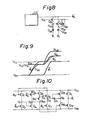
- Fig. 8 an example of the high level clock signal generating circuit is shown
- Fig. 9 the waveforms of each of the portions at operation in the circuit are shown.
- a clock generator CG generates a clock signal which has the same phase as the clock signal ⁇ 1 corresponding to the inverted signal of the clock signal ⁇ 1 and has an amplitude of from Vss to Vcc.
- the above--mentioned generated clock signal is shown as a curve below the Vcc line in Fig. 9.
- the transistor Q23 always charges the node N21 to the (Vcc - Vth).
- a third embodiment of the present invention is shown.
- the transistor Q5 in Fig. 1 is replaced with two transistors Q51 and Q52.
- the inverted clock signal ⁇ 0 the high level of which is the Vcc
- the transistor Q3 turns on, the voltage of the node N2 is equal to the (Vcc - Vth), the transistor Q51 turns on, and the voltage of the node N3 is euqal to the (Vcc - Vth).
- the above-mentioned high level clock signal is applied to the gates of the transistors Q3 and Q51, and, similar to the first and the second embodiments, the voltage of the nodes N2 and N3 (the first node and the third node) corresponds to the Vcc during the standby period.
- the transistor Q13 in Figs. 4 and 5 is not necessary; nevertheless, the operation waveforms are similar to the waveforms in Figs. 6 and 7.
Landscapes
- Engineering & Computer Science (AREA)
- Computer Hardware Design (AREA)
- Physics & Mathematics (AREA)
- Computing Systems (AREA)
- General Engineering & Computer Science (AREA)
- Mathematical Physics (AREA)
- Microelectronics & Electronic Packaging (AREA)
- Nonlinear Science (AREA)
- Logic Circuits (AREA)
- Dram (AREA)
- Electronic Switches (AREA)
- Manipulation Of Pulses (AREA)
Abstract
Description
- The present invention relates, for example, to a semiconductor circuit used as a buffer circuit having the function of compensating for a power source fluctuation and used for the amplification of a clock signal in a dynamic memory device.
- A conventional buffer circuit which amplifies an input clock signal $0 (conversion of impedance) and supplies an output clock signal φ1 is constituted of MOS transistors Q1 through Q12 (Q9 is a MOS capacitor), as shown in Fig. 1. The input stage of the buffer circuit is a delay circuit constituted of transistors Ql through Q4. During a standby period, the delay circuit holds the voltage of the node N2, which connects the source of transistor Q3 with the drain of transistor Q4, at a high level. This is possible because of the input clock signal $0 and the inverted input clock signal 0. The clock signal φ0 is at a high level during an active period and is at a low level during the standby period. The clock signal
Φ 0 , because of the inverted polarity, is at a low level during the active period and is at a high level during the standby period. These clock signals turn off the transistor Ql, turn on the transistors Q2 and Q3, hold the node N1 at a low level, which node N1 connects the source of the transistor Q1 with the drain of the transistor Q2 and the gate of the transistor Q4, turn off the transistor Q4, and charge the node N2 to the voltage of (Vcc-Vth) through the transistor Q3 during the standby period. The Vcc is the voltage on the high voltage side of the power source and is usually 5 volts, which is the standard value allowing for an error of ±10%. The Vth is a threshold value of the transistor. Since the gate of the transistor Q5 is connected to the power source Vcc, when the node N2 is charged to the (Vcc-Vth) the node N3 is charged to the same voltage. The node N3, which connects the transistor Q5 with the gate of transistor Q6, is the gate terminal of the transistor Q6 in the bootstrap circuit including the transistors Q6 and Q7. By charging the node N3 to a high level during the standby period, the charged voltage of the node N3 drives, at a high speed, the output stage including the transistors Q8 through Q12 during the next active period. Since the clock signalΦ is at a high level during the standby period, the transistor Q7 turns on, the node N4 which connects the source of transistor Q6 with the drain of the transistor Q7, the MOS capacitor Q9, and the gate of transistor Qll reaches a low level, the transistors Q8 and Qll turn off, the transistors Q10 and Q12 turn on, and the output clock signal $1 is at a low level which is equal to the low voltage side of the power source Vss (usually ground voltage). - At the start of the active period, the input clock signals φ0 and0 are inverted. In Fig. 2, waveforms are shown during the active period. This example shows a constant Vcc which is equal to 4.5 volts. Although, in this example, the voltage of the node N2 is equal to the voltage of the node N3 (4.5 volts-Vth) at the end of the standby period, when the clock signal
 0 changes from Vcc to Vss and the clock signal $0 changes from Vss to Vcc, the voltage of the node N3 increases to more than (Vcc + Vth) and the voltage of the node N4 is charged to the voltage of φ0 , which is equal to Vcc, by means of the bootstrap effect, which is due to the effects of the capacity between the gate and the drain of the transistor Q6 and between the gate and the source of the transistor Q6.
 - This results in the transistors Q8 and Qll being turned on. At the same time, since the transistor Ql turns on, the transistor Q2 turns off, and the node N1 is charged to a voltage of Vcc; then the transistor Q4 turns on and the voltage of the node N2 begins to decrease. Accordingly, the electric charges at the node N3 are attracted by the voltage of node N2 through the transistor Q5 and the voltage of the nodes N3 and N2 decreases to Vss. When the voltage of the node N2 decreases to (Vss + Vth), the transistors Q10 and Q12 turn off and the voltage of the node N5 increases to Vcc. At this time, since the voltage of the node N3 is Vss, the transistor Q6 turns off and the voltage of the node N4 is increased to more than (Vcc + Vth) through the capacitor Q9, the output clock signal φ1 increases to the maximum power source voltage level Vcc.
- The above-mentioned operation is carried out when no fluctuation of the power source occurs. However, if fluctuation of the power source occurs during the standby period, as shown in Fig. 3, the output clock signal $1 is delayed, and delay of the output clock signal φ1 signifies a problem. In Fig. 3 an example is shown in which the Vcc decreases from 5.5 volts (Vcc(U)) to 4.5 volts (Vcc(L)) during the standby period. The above-mentioned fluctuation occurs when the electrical constitution of the constant voltage power supply is simplified in order to reduce the cost of the device or when other devices connected to the same power source are operated. During the standby period, the voltage of the clock signal $0 is low, the voltage of the clock signal0 is high and the voltage of Vcc is the upper limit Vcc(U), which is equal to 5.5 volts, causing both the nodes N2 and N3 to be charged to (5.5 volts-Vth). Further, if the Vcc decreases to the lower limit Vcc(L) which is equal to 4.5 volts, during the standby period, the voltage of the nodes N2 and N3 (5.5 volts-Vth) does not change because there is no discharge path. The reason there is no discharge path is that the transistor Q4 is in the "off" state, and the gate of the transistor Q3 has a low voltage of 4.5 volts which is equal to φ0 and Vcc. When the voltage of the nodes N2 and N3 is held, the clock signal φ1 is delayed. In order to increase the clock signal φ1 , it is necessary that the transistors Q10 and Q12 be turned off; on the other hand, it takes time for the voltage of the node N2 to decrease to the low level (Vss + Vth) at which the transistors Q10 and Q12 are turned off because the initial voltage of the node N2 is (5.5 volts-Vth), that is, it is 1 volt higher than the voltage (4.5 volts-Vth) in Fig. 2. During the period of delay when the voltage is decreasing at the node N2, a delay in the clock signal $1 occurs. In Fig. 3 the waveforms indicated by the broken lines N2', N3', N5' and φ1' show the passages of the voltage changes at the nodes N2, N3 and N5 and the voltage of the clock signal φ1 without a power source fluctuation, as compared with the lines N2, N3, N5 and φ1 which show the passages of the voltage changes at the nodes N2, N3 and N5 when fluctuation occurs in the power supply.
- The prior art regarding the above-mentioned method is disclosed in U.S.P. No. 4,061,933.
- The present invention is proposed in order to reduce the above-mentioned problems.
- An embodiment of the present invention can provide a semiconductor circuit used as a buffer circuit in which the voltage of the charged nodes during the standby period corresponds to the voltage of the power source throughout the standby period, thereby improving the delay in the output clock signal caused by fluctuation of the voltage of the power supply and accomplishing high speed access time in a dynamic memory device.
- According to one aspect of the present invention, there is provided a semiconductor circuit used as a buffer circuit comprising an input stage circuit for receiving an input clock signal and an inverted input clock signal, a bootstrap circuit, comprising a transistor, for receiving the output of said input stage circuit and for maintaining the gate voltage of said transistor at a high level during a standby period, and an output circuit comprising a transistoi, which is switched on and off by the output of said bootstrap circuit and said input stage circuit, for generating an output clock signal, said semiconductor circuit further comprising a means by which a high level clock signal, having the same phase as said inverted clock signal and a level higher than the level of the sum of a power source voltage and a transistor threshold voltage, is applied to a gate of a predetermined transistor, whereby the voltage of a point charged during the standby period corresponds to the voltage of the power source throughout the standby period.
- According to another aspect of the present invention, there is provided a semiconductor circuit used as a buffer circuit comprising an input stage delay circuit for receiving an input clock signal and an inverted input clock signal, a bootstrap circuit for receiving the output of said input stage delay circuit, said bootstrap circuit increasing the voltage of an output by means of a bootstrap operation, and an output circuit for receiving the output of said bootstrap circuit and said input stage delay circuit and for generating an output clock signal, said semiconductor circuit further comprising a means by which a high level clock signal, having the same phase as said inverted clock signal and a level higher than the level of the sum of a power source voltage and a transistor threshold voltage, is applied to a gate of a transistor for connecting a first node connecting the output of said input stage delay circuit with the input of said bootstrap circuit with one of the output terminals of the power source, whereby the voltage of said first node corresponds to the power source throughout the standby period.
- According to still another aspect of the present invention, there is provided a semiconductor circuit used as a buffer circuit comprising an input stage delay circuit for receiving an input clock signal and an inverted input clock signal, a bootstrap circuit for receiving the output of said input stage delay circuit, said bootstrap circuit increasing the voltage of an output by means of a bootstrap operation, said bootstrap circuit comprising at least two transistors in a first stage and a transistor in a second stage, and an output circuit for receiving the output of said bootstrap circuit and said input stage delay circuit and for generating an output clock signal, said semiconductor circuit further comprising a means by which a high level clock signal, having the same phase as said inverted clock signal and a level higher than the level of the sum of a power source voltage and a transistor threshold voltage, is applied to the gate of the transistor for connecting the first node connecting the output of said input stage delay circuit with the input of said bootstrap circuit, with one of the output terminals of the power source, and another means by which said high level clock signal is applied to the gate of the transistor for connecting the third node connecting the two transistors in said first tage with the transistor in said second stage, with one of the output terminals of the power source, whereby the voltage of said first node and said third node corresponds to the power source throughout the standby period.
-
- Figure 1 shows a circuit diagram of an example of a conventional clock signal amplifier circuit;
- Fig. 2 and Fig. 3 are waveform diagrams of the circuit of Fig. 1;
- Fig. 4 shows a circuit diagram of a semiconductor circuit used as a buffer circuit according to a first embodiment of the present invention;
- Fig. 5 shows a circuit diagram of a semiconductor circuit used as a buffer circuit according to a second embodiment of the present invention;
- Fig. 6 and Fig. 7 are waveform diagrams of the circuits of Fig. 4 and Fig. 5;
- Fig. 8 shows an example of a circuit diagram of a high level clock signal generator, the output of which is used at the circuits according to the embodiments of the present invention;
- Fig. 9 is a waveform diagram of the high level clock generating circuit in Fig. 8;
- Fig. 10 shows a circuit diagram of a semiconductor circuit used as a buffer circuit according to a third embodiment of the present invention.
- In Fig. 4 and Fig. 5, circuit diagrams of a semiconductor circuit used as a buffer circuit are shown, according to a first embodiment and a second embodiment of the present invention, respectively. In the Figures the same elements as those in the circuit of Fig. 1 are referred to by the same reference numbers as in Fig. 1. There are two ways in which the above-mentioned circuits of the embodiments differ from the circuit of Fig. 1. In regard to the first way, a high level clock signal'0 which is the same phase as said inverted clock signal0 and the high level of which is higher than the level of the sum of the power source voltage Vcc and the transistor threshold voltage Vth, is applied to the gate of the transistor Q3 through which the node N2 is charged in an input stage circuit during the standby period. In regard to the second way, another transistor Q13, to the gate of which the high level clock signal is similarly applied, is connected between the node N2 and the N3 in the example shown in Fig. 4 or between one of the output terminals of the power source Vcc and the node N3 in the example shown in Fig. 5. The other circuitry is the same as that of Fig. 1 and therefore explanations regarding the same portions are abbreviated. In these embodiments, the node N2 is the first node and the node N3 is the second node.
- When the high level clock signal'0 , the high level of which is equal to more than (Vcc + Vth), is applied to the gate of the transistor Q , the voltage of the node N2 corresponds to the Vcc during the standby period. Therefore, in the case in which the Vcc is constantly 4.5 volts, as shown in Fig. 6, or in the case in which the Vcc decreases from 5.5 volts to -4.5 volts during the standby period, as shown in Fig. 7, the active period begins when the voltage of N2 is equal to 4.5 volts. Namely, if the voltage of N2 is charged to 5.5 volts when the Vcc is 5.5 volts, the charges at the node N2 can discharge to the side of the Vcc line through the transistor Q3 when the Vcc decreases to 4.5 volts, resulting in a decrease in the voltage of the node N2 to 4.5 volts. Accordingly, the voltage of the node N2, which voltage turns off the transistors Q10 and Q12 in the output stage during the active period, is defined according to the Vcc at the end of the standby period whether fluctuation of the power source occurs or not. Therefore, there is no difference in the voltage change between the node N2 in Fig. 6 and the node N2 in Fig. 7 during the active period. The factor responsible for delay of the clock signal $1 in the case of Fig. 7, as compared with Fig. 6, is improved. The effect is further emphasized by the addition of transistor Q13 so that the voltage of the node N3 also corresponds to the Vcc. In these embodiments, since the node N2 is charged at a high level, as much as a Vth higher than the voltage of the node N2 in Fig. 1, the channel width of the trasistor Q4 must be increased so as to decrease the discharge time. The broken line $l in Fig. 7 shows the delay of the clock signal φ1 when a conventional circuit is used.
- In Fig. 8 an example of the high level clock signal

φ 1 corresponding to the inverted signal of the clock signal φ1 and has an amplitude of from Vss to Vcc. The above--mentioned generated clock signal is shown as a curve


φ 1 increases to the Vcc; then the voltage of the node N21 is increased through the capacitor Q24. Further, by the bootstrap effect by means of the capacitor Q25, the voltage of the node N22 is increased; then the transistor Q22 turns on sufficiently, the charges at the node N21 are discharged to the output side, and the high level clock signal φ'0 is amplified to more than (Vcc + Vth). - In Fig. 10, a third embodiment of the present invention is shown. In the circuit of this embodiment, the transistor Q5 in Fig. 1 is replaced with two transistors Q51 and Q52. In this circuit, the inverted clock signal φ0 , the high level of which is the Vcc, is usually applied to the gates of transistors Q3 and Q51. Accordingly, since the inverted clock signal0 is at a high level during the standby period, the transistor Q3 turns on, the voltage of the node N2 is equal to the (Vcc - Vth), the transistor Q51 turns on, and the voltage of the node N3 is euqal to the (Vcc - Vth). While the clock signal φ0 is at a low level, the transistor Q52 turns off and the node N2 is electrically separated from the node N3. During the active period, the clock signal $0 is at a high level and the transistor Q52 turns on, and an operation similar to that shown in Fig. 1 is carried out. When the Vcc fluctuates before the active period, similar in operation to that shown in Fig. 1, the voltage of the nodes N2 and N3 remains excessively high.
- In this embodiment, the above-mentioned high level clock signal ;; , the high level of which is more than the (Vcc + Vth), is applied to the gates of the transistors Q3 and Q51, and, similar to the first and the second embodiments, the voltage of the nodes N2 and N3 (the first node and the third node) corresponds to the Vcc during the standby period. In this semiconductor circuit used as a buffer circuit, the transistor Q13 in Figs. 4 and 5 is not necessary; nevertheless, the operation waveforms are similar to the waveforms in Figs. 6 and 7.
Claims (6)
Applications Claiming Priority (2)
| Application Number | Priority Date | Filing Date | Title |
|---|---|---|---|
| JP183075/80 | 1980-12-24 | ||
| JP55183075A JPS57106228A (en) | 1980-12-24 | 1980-12-24 | Semiconductor circuit |
Publications (3)
| Publication Number | Publication Date |
|---|---|
| EP0055136A2 true EP0055136A2 (en) | 1982-06-30 |
| EP0055136A3 EP0055136A3 (en) | 1982-08-11 |
| EP0055136B1 EP0055136B1 (en) | 1985-04-17 |
Family
ID=16129309
Family Applications (1)
| Application Number | Title | Priority Date | Filing Date |
|---|---|---|---|
| EP81306074A Expired EP0055136B1 (en) | 1980-12-24 | 1981-12-23 | A semiconductor buffer circuit |
Country Status (5)
| Country | Link |
|---|---|
| US (1) | US4443714A (en) |
| EP (1) | EP0055136B1 (en) |
| JP (1) | JPS57106228A (en) |
| DE (1) | DE3170062D1 (en) |
| IE (1) | IE52382B1 (en) |
Cited By (7)
| Publication number | Priority date | Publication date | Assignee | Title |
|---|---|---|---|---|
| EP0105662A3 (en) * | 1982-09-28 | 1985-05-15 | Fujitsu Limited | Buffer circuit with boot-strap circuit |
| EP0058509B1 (en) * | 1981-02-12 | 1987-05-13 | Fujitsu Limited | Semiconductor circuit for driving clock signal line |
| EP0237139A1 (en) * | 1986-01-08 | 1987-09-16 | Kabushiki Kaisha Toshiba | Buffer circuit for integrated circuit |
| EP0202025A3 (en) * | 1985-04-13 | 1988-08-03 | Fujitsu Limited | Booster circuit |
| EP0383289A1 (en) * | 1989-02-17 | 1990-08-22 | Texas Instruments Deutschland Gmbh | Integrated push-pull output stage |
| WO2007042970A1 (en) * | 2005-10-07 | 2007-04-19 | Nxp B.V. | Single threshold and single conductivity type amplifier/buffer |
| US7362139B2 (en) | 2001-07-30 | 2008-04-22 | Semiconductor Energy Laboratory Co., Ltd. | Semiconductor device |
Families Citing this family (11)
| Publication number | Priority date | Publication date | Assignee | Title |
|---|---|---|---|---|
| JPS599735A (en) * | 1982-07-07 | 1984-01-19 | Mitsubishi Electric Corp | Clock generating circuit |
| JPS60111391A (en) * | 1983-11-21 | 1985-06-17 | Nec Corp | Output circuit of semiconductor |
| JPS60140924A (en) * | 1983-12-27 | 1985-07-25 | Nec Corp | Semiconductor circuit |
| US4642492A (en) * | 1984-10-25 | 1987-02-10 | Digital Equipment Corporation | Multiple phase clock buffer module with non-saturated pull-up transistor to avoid hot electron effects |
| US4797573A (en) * | 1984-11-21 | 1989-01-10 | Nec Corporation | Output circuit with improved timing control circuit |
| JPH02161813A (en) * | 1988-12-14 | 1990-06-21 | Nec Corp | Rs232c line driver ic |
| KR0170511B1 (en) * | 1995-11-09 | 1999-03-30 | 김광호 | Charge pump circuit for mos transistor driving |
| JP5665299B2 (en) * | 2008-10-31 | 2015-02-04 | 三菱電機株式会社 | Shift register circuit |
| JP5188382B2 (en) | 2008-12-25 | 2013-04-24 | 三菱電機株式会社 | Shift register circuit |
| JP6628837B2 (en) * | 2018-06-15 | 2020-01-15 | 株式会社半導体エネルギー研究所 | Electronics |
| WO2020128713A1 (en) | 2018-12-20 | 2020-06-25 | 株式会社半導体エネルギー研究所 | Logic circuit configured using unipolar transistors, and semiconductor device |
Family Cites Families (9)
| Publication number | Priority date | Publication date | Assignee | Title |
|---|---|---|---|---|
| US3909631A (en) * | 1973-08-02 | 1975-09-30 | Texas Instruments Inc | Pre-charge voltage generating system |
| US3927334A (en) * | 1974-04-11 | 1975-12-16 | Electronic Arrays | MOSFET bistrap buffer |
| JPS5649021B2 (en) * | 1975-02-19 | 1981-11-19 | ||
| US4061999A (en) * | 1975-12-29 | 1977-12-06 | Mostek Corporation | Dynamic random access memory system |
| US4061933A (en) * | 1975-12-29 | 1977-12-06 | Mostek Corporation | Clock generator and delay stage |
| DE2641693C2 (en) * | 1976-09-16 | 1978-11-16 | Siemens Ag, 1000 Berlin Und 8000 Muenchen | Decoding circuit with MOS transistors |
| JPS5513566A (en) * | 1978-07-17 | 1980-01-30 | Hitachi Ltd | Mis field effect semiconductor circuit device |
| US4317051A (en) * | 1979-10-09 | 1982-02-23 | Bell Telephone Laboratories, Incorporated | Clock generator (buffer) circuit |
| WO1982000930A1 (en) * | 1980-09-10 | 1982-03-18 | Plachno R | Delay stage for a clock generator |
-
1980
- 1980-12-24 JP JP55183075A patent/JPS57106228A/en active Granted
-
1981
- 1981-12-16 US US06/331,476 patent/US4443714A/en not_active Expired - Lifetime
- 1981-12-23 IE IE3068/81A patent/IE52382B1/en not_active IP Right Cessation
- 1981-12-23 EP EP81306074A patent/EP0055136B1/en not_active Expired
- 1981-12-23 DE DE8181306074T patent/DE3170062D1/en not_active Expired
Cited By (11)
| Publication number | Priority date | Publication date | Assignee | Title |
|---|---|---|---|---|
| EP0058509B1 (en) * | 1981-02-12 | 1987-05-13 | Fujitsu Limited | Semiconductor circuit for driving clock signal line |
| EP0105662A3 (en) * | 1982-09-28 | 1985-05-15 | Fujitsu Limited | Buffer circuit with boot-strap circuit |
| EP0202025A3 (en) * | 1985-04-13 | 1988-08-03 | Fujitsu Limited | Booster circuit |
| EP0237139A1 (en) * | 1986-01-08 | 1987-09-16 | Kabushiki Kaisha Toshiba | Buffer circuit for integrated circuit |
| EP0383289A1 (en) * | 1989-02-17 | 1990-08-22 | Texas Instruments Deutschland Gmbh | Integrated push-pull output stage |
| US7362139B2 (en) | 2001-07-30 | 2008-04-22 | Semiconductor Energy Laboratory Co., Ltd. | Semiconductor device |
| USRE41215E1 (en) | 2001-07-30 | 2010-04-13 | Semiconductor Energy Laboratory Co., Ltd. | Semiconductor device |
| USRE43401E1 (en) | 2001-07-30 | 2012-05-22 | Semiconductor Energy Laboratory Co., Ltd. | Semiconductor device |
| USRE44657E1 (en) | 2001-07-30 | 2013-12-24 | Semiconductor Energy Laboratory Co., Ltd. | Semiconductor device |
| WO2007042970A1 (en) * | 2005-10-07 | 2007-04-19 | Nxp B.V. | Single threshold and single conductivity type amplifier/buffer |
| US7834668B2 (en) | 2005-10-07 | 2010-11-16 | Nxp B.V. | Single threshold and single conductivity type amplifier/buffer |
Also Published As
| Publication number | Publication date |
|---|---|
| JPS57106228A (en) | 1982-07-02 |
| IE52382B1 (en) | 1987-10-14 |
| JPH0216057B2 (en) | 1990-04-16 |
| IE813068L (en) | 1982-06-24 |
| US4443714A (en) | 1984-04-17 |
| DE3170062D1 (en) | 1985-05-23 |
| EP0055136B1 (en) | 1985-04-17 |
| EP0055136A3 (en) | 1982-08-11 |
Similar Documents
| Publication | Publication Date | Title |
|---|---|---|
| EP0055136A2 (en) | A semiconductor buffer circuit | |
| JPH02177716A (en) | Boosting circuit | |
| EP0052504B1 (en) | Semiconductor buffer circuit | |
| JPH0427731B2 (en) | ||
| US4443720A (en) | Bootstrap circuit | |
| US5369320A (en) | Bootstrapped high-speed output buffer | |
| JPH0334150B2 (en) | ||
| US4239991A (en) | Clock voltage generator for semiconductor memory | |
| US6225853B1 (en) | Booster circuit | |
| US5134317A (en) | Booster circuit for a semiconductor memory device | |
| JP3162591B2 (en) | Semiconductor integrated circuit | |
| EP0069444B1 (en) | Trigger pulse generator | |
| US4352996A (en) | IGFET Clock generator circuit employing MOS boatstrap capacitive drive | |
| US4716303A (en) | MOS IC pull-up circuit | |
| US4468576A (en) | Inverter circuit having transistors operable in a shallow saturation region for avoiding fluctuation of electrical characteristics | |
| US4239990A (en) | Clock voltage generator for semiconductor memory with reduced power dissipation | |
| JPS595488A (en) | Semiconductor device | |
| JPH0245275B2 (en) | ||
| EP0061271A1 (en) | MOS dynamic memory device | |
| US4529889A (en) | Sense amplifier latch voltage waveform generator circuit | |
| KR100432985B1 (en) | Circuit for generating increased output voltage | |
| JPS61198813A (en) | Clock generator circuit | |
| US5638023A (en) | Charge pump circuit | |
| EP0109004A2 (en) | Low power clock generator | |
| JPH097371A (en) | Boost voltage supply circuit |
Legal Events
| Date | Code | Title | Description |
|---|---|---|---|
| PUAI | Public reference made under article 153(3) epc to a published international application that has entered the european phase |
Free format text: ORIGINAL CODE: 0009012 |
|
| PUAL | Search report despatched |
Free format text: ORIGINAL CODE: 0009013 |
|
| AK | Designated contracting states |
Designated state(s): DE FR GB NL |
|
| AK | Designated contracting states |
Designated state(s): DE FR GB NL |
|
| 17P | Request for examination filed |
Effective date: 19830131 |
|
| GRAA | (expected) grant |
Free format text: ORIGINAL CODE: 0009210 |
|
| AK | Designated contracting states |
Designated state(s): DE FR GB NL |
|
| REF | Corresponds to: |
Ref document number: 3170062 Country of ref document: DE Date of ref document: 19850523 |
|
| ET | Fr: translation filed | ||
| PLBE | No opposition filed within time limit |
Free format text: ORIGINAL CODE: 0009261 |
|
| STAA | Information on the status of an ep patent application or granted ep patent |
Free format text: STATUS: NO OPPOSITION FILED WITHIN TIME LIMIT |
|
| 26N | No opposition filed | ||
| PGFP | Annual fee paid to national office [announced via postgrant information from national office to epo] |
Ref country code: FR Payment date: 19921221 Year of fee payment: 12 |
|
| PGFP | Annual fee paid to national office [announced via postgrant information from national office to epo] |
Ref country code: NL Payment date: 19921231 Year of fee payment: 12 |
|
| PGFP | Annual fee paid to national office [announced via postgrant information from national office to epo] |
Ref country code: DE Payment date: 19930226 Year of fee payment: 12 |
|
| PG25 | Lapsed in a contracting state [announced via postgrant information from national office to epo] |
Ref country code: NL Effective date: 19940701 |
|
| NLV4 | Nl: lapsed or anulled due to non-payment of the annual fee | ||
| PG25 | Lapsed in a contracting state [announced via postgrant information from national office to epo] |
Ref country code: FR Effective date: 19940831 |
|
| PG25 | Lapsed in a contracting state [announced via postgrant information from national office to epo] |
Ref country code: DE Effective date: 19940901 |
|
| REG | Reference to a national code |
Ref country code: FR Ref legal event code: ST |
|
| PGFP | Annual fee paid to national office [announced via postgrant information from national office to epo] |
Ref country code: GB Payment date: 19951214 Year of fee payment: 15 |
|
| PG25 | Lapsed in a contracting state [announced via postgrant information from national office to epo] |
Ref country code: GB Effective date: 19961223 |
|
| GBPC | Gb: european patent ceased through non-payment of renewal fee |
Effective date: 19961223 |