DE112017002426B4 - Method for producing an optoelectronic component and optoelectronic component - Google Patents
Method for producing an optoelectronic component and optoelectronic component Download PDFInfo
- Publication number
- DE112017002426B4 DE112017002426B4 DE112017002426.9T DE112017002426T DE112017002426B4 DE 112017002426 B4 DE112017002426 B4 DE 112017002426B4 DE 112017002426 T DE112017002426 T DE 112017002426T DE 112017002426 B4 DE112017002426 B4 DE 112017002426B4
- Authority
- DE
- Germany
- Prior art keywords
- semiconductor chip
- converter element
- optoelectronic component
- advantageously
- producing
- Prior art date
- Legal status (The legal status is an assumption and is not a legal conclusion. Google has not performed a legal analysis and makes no representation as to the accuracy of the status listed.)
- Active
Links
- 230000005693 optoelectronics Effects 0.000 title claims abstract description 39
- 238000004519 manufacturing process Methods 0.000 title claims abstract description 23
- 239000004065 semiconductor Substances 0.000 claims abstract description 187
- 239000000758 substrate Substances 0.000 claims abstract description 32
- 229910052594 sapphire Inorganic materials 0.000 claims abstract description 30
- 239000010980 sapphire Substances 0.000 claims abstract description 30
- 238000000034 method Methods 0.000 claims description 60
- 239000002131 composite material Substances 0.000 claims description 27
- 239000000463 material Substances 0.000 claims description 16
- 238000005538 encapsulation Methods 0.000 claims description 15
- 230000005855 radiation Effects 0.000 claims description 12
- 239000011521 glass Substances 0.000 claims description 8
- 238000000926 separation method Methods 0.000 claims description 7
- 239000000919 ceramic Substances 0.000 claims description 5
- 238000005520 cutting process Methods 0.000 claims description 3
- 101100001671 Emericella variicolor andF gene Proteins 0.000 abstract 1
- 239000010410 layer Substances 0.000 description 64
- 239000012790 adhesive layer Substances 0.000 description 10
- 238000000231 atomic layer deposition Methods 0.000 description 4
- 238000010521 absorption reaction Methods 0.000 description 3
- 230000000694 effects Effects 0.000 description 3
- 229910052709 silver Inorganic materials 0.000 description 3
- 239000004332 silver Substances 0.000 description 3
- 229910052581 Si3N4 Inorganic materials 0.000 description 2
- VYPSYNLAJGMNEJ-UHFFFAOYSA-N Silicium dioxide Chemical compound O=[Si]=O VYPSYNLAJGMNEJ-UHFFFAOYSA-N 0.000 description 2
- 230000032683 aging Effects 0.000 description 2
- XAGFODPZIPBFFR-UHFFFAOYSA-N aluminium Chemical compound [Al] XAGFODPZIPBFFR-UHFFFAOYSA-N 0.000 description 2
- 229910052782 aluminium Inorganic materials 0.000 description 2
- PNEYBMLMFCGWSK-UHFFFAOYSA-N aluminium oxide Inorganic materials [O-2].[O-2].[O-2].[Al+3].[Al+3] PNEYBMLMFCGWSK-UHFFFAOYSA-N 0.000 description 2
- 150000001875 compounds Chemical class 0.000 description 2
- 229910052593 corundum Inorganic materials 0.000 description 2
- 230000001419 dependent effect Effects 0.000 description 2
- 238000011161 development Methods 0.000 description 2
- 230000018109 developmental process Effects 0.000 description 2
- 239000010931 gold Substances 0.000 description 2
- 150000004767 nitrides Chemical class 0.000 description 2
- 239000011368 organic material Substances 0.000 description 2
- 230000035515 penetration Effects 0.000 description 2
- 229920001296 polysiloxane Polymers 0.000 description 2
- HQVNEWCFYHHQES-UHFFFAOYSA-N silicon nitride Chemical compound N12[Si]34N5[Si]62N3[Si]51N64 HQVNEWCFYHHQES-UHFFFAOYSA-N 0.000 description 2
- 229910052814 silicon oxide Inorganic materials 0.000 description 2
- 238000004528 spin coating Methods 0.000 description 2
- 229910001845 yogo sapphire Inorganic materials 0.000 description 2
- 229920002799 BoPET Polymers 0.000 description 1
- 239000005041 Mylar™ Substances 0.000 description 1
- 239000000853 adhesive Substances 0.000 description 1
- 238000004026 adhesive bonding Methods 0.000 description 1
- 230000001070 adhesive effect Effects 0.000 description 1
- 238000006243 chemical reaction Methods 0.000 description 1
- 239000003086 colorant Substances 0.000 description 1
- 239000002019 doping agent Substances 0.000 description 1
- PCHJSUWPFVWCPO-UHFFFAOYSA-N gold Chemical compound [Au] PCHJSUWPFVWCPO-UHFFFAOYSA-N 0.000 description 1
- 229910052737 gold Inorganic materials 0.000 description 1
- 239000000203 mixture Substances 0.000 description 1
- 230000000704 physical effect Effects 0.000 description 1
- 238000007747 plating Methods 0.000 description 1
- 229920000728 polyester Polymers 0.000 description 1
- 238000007788 roughening Methods 0.000 description 1
- 230000035882 stress Effects 0.000 description 1
- 239000000725 suspension Substances 0.000 description 1
Images


Classifications
-
- H—ELECTRICITY
- H10—SEMICONDUCTOR DEVICES; ELECTRIC SOLID-STATE DEVICES NOT OTHERWISE PROVIDED FOR
- H10H—INORGANIC LIGHT-EMITTING SEMICONDUCTOR DEVICES HAVING POTENTIAL BARRIERS
- H10H20/00—Individual inorganic light-emitting semiconductor devices having potential barriers, e.g. light-emitting diodes [LED]
- H10H20/80—Constructional details
- H10H20/85—Packages
- H10H20/851—Wavelength conversion means
- H10H20/8514—Wavelength conversion means characterised by their shape, e.g. plate or foil
-
- H—ELECTRICITY
- H10—SEMICONDUCTOR DEVICES; ELECTRIC SOLID-STATE DEVICES NOT OTHERWISE PROVIDED FOR
- H10H—INORGANIC LIGHT-EMITTING SEMICONDUCTOR DEVICES HAVING POTENTIAL BARRIERS
- H10H20/00—Individual inorganic light-emitting semiconductor devices having potential barriers, e.g. light-emitting diodes [LED]
- H10H20/01—Manufacture or treatment
- H10H20/011—Manufacture or treatment of bodies, e.g. forming semiconductor layers
- H10H20/018—Bonding of wafers
-
- H—ELECTRICITY
- H10—SEMICONDUCTOR DEVICES; ELECTRIC SOLID-STATE DEVICES NOT OTHERWISE PROVIDED FOR
- H10H—INORGANIC LIGHT-EMITTING SEMICONDUCTOR DEVICES HAVING POTENTIAL BARRIERS
- H10H20/00—Individual inorganic light-emitting semiconductor devices having potential barriers, e.g. light-emitting diodes [LED]
- H10H20/80—Constructional details
- H10H20/83—Electrodes
-
- H—ELECTRICITY
- H10—SEMICONDUCTOR DEVICES; ELECTRIC SOLID-STATE DEVICES NOT OTHERWISE PROVIDED FOR
- H10H—INORGANIC LIGHT-EMITTING SEMICONDUCTOR DEVICES HAVING POTENTIAL BARRIERS
- H10H20/00—Individual inorganic light-emitting semiconductor devices having potential barriers, e.g. light-emitting diodes [LED]
- H10H20/80—Constructional details
- H10H20/84—Coatings, e.g. passivation layers or antireflective coatings
- H10H20/841—Reflective coatings, e.g. dielectric Bragg reflectors
-
- H—ELECTRICITY
- H10—SEMICONDUCTOR DEVICES; ELECTRIC SOLID-STATE DEVICES NOT OTHERWISE PROVIDED FOR
- H10H—INORGANIC LIGHT-EMITTING SEMICONDUCTOR DEVICES HAVING POTENTIAL BARRIERS
- H10H20/00—Individual inorganic light-emitting semiconductor devices having potential barriers, e.g. light-emitting diodes [LED]
- H10H20/80—Constructional details
- H10H20/85—Packages
- H10H20/852—Encapsulations
- H10H20/853—Encapsulations characterised by their shape
-
- H—ELECTRICITY
- H10—SEMICONDUCTOR DEVICES; ELECTRIC SOLID-STATE DEVICES NOT OTHERWISE PROVIDED FOR
- H10H—INORGANIC LIGHT-EMITTING SEMICONDUCTOR DEVICES HAVING POTENTIAL BARRIERS
- H10H20/00—Individual inorganic light-emitting semiconductor devices having potential barriers, e.g. light-emitting diodes [LED]
- H10H20/01—Manufacture or treatment
- H10H20/036—Manufacture or treatment of packages
- H10H20/0361—Manufacture or treatment of packages of wavelength conversion means
-
- H—ELECTRICITY
- H10—SEMICONDUCTOR DEVICES; ELECTRIC SOLID-STATE DEVICES NOT OTHERWISE PROVIDED FOR
- H10H—INORGANIC LIGHT-EMITTING SEMICONDUCTOR DEVICES HAVING POTENTIAL BARRIERS
- H10H20/00—Individual inorganic light-emitting semiconductor devices having potential barriers, e.g. light-emitting diodes [LED]
- H10H20/01—Manufacture or treatment
- H10H20/036—Manufacture or treatment of packages
- H10H20/0362—Manufacture or treatment of packages of encapsulations
-
- H—ELECTRICITY
- H10—SEMICONDUCTOR DEVICES; ELECTRIC SOLID-STATE DEVICES NOT OTHERWISE PROVIDED FOR
- H10H—INORGANIC LIGHT-EMITTING SEMICONDUCTOR DEVICES HAVING POTENTIAL BARRIERS
- H10H20/00—Individual inorganic light-emitting semiconductor devices having potential barriers, e.g. light-emitting diodes [LED]
- H10H20/80—Constructional details
- H10H20/81—Bodies
- H10H20/822—Materials of the light-emitting regions
- H10H20/824—Materials of the light-emitting regions comprising only Group III-V materials, e.g. GaP
- H10H20/825—Materials of the light-emitting regions comprising only Group III-V materials, e.g. GaP containing nitrogen, e.g. GaN
-
- H—ELECTRICITY
- H10—SEMICONDUCTOR DEVICES; ELECTRIC SOLID-STATE DEVICES NOT OTHERWISE PROVIDED FOR
- H10H—INORGANIC LIGHT-EMITTING SEMICONDUCTOR DEVICES HAVING POTENTIAL BARRIERS
- H10H20/00—Individual inorganic light-emitting semiconductor devices having potential barriers, e.g. light-emitting diodes [LED]
- H10H20/80—Constructional details
- H10H20/85—Packages
- H10H20/851—Wavelength conversion means
-
- H—ELECTRICITY
- H10—SEMICONDUCTOR DEVICES; ELECTRIC SOLID-STATE DEVICES NOT OTHERWISE PROVIDED FOR
- H10H—INORGANIC LIGHT-EMITTING SEMICONDUCTOR DEVICES HAVING POTENTIAL BARRIERS
- H10H20/00—Individual inorganic light-emitting semiconductor devices having potential barriers, e.g. light-emitting diodes [LED]
- H10H20/80—Constructional details
- H10H20/85—Packages
- H10H20/852—Encapsulations
- H10H20/854—Encapsulations characterised by their material, e.g. epoxy or silicone resins
-
- H—ELECTRICITY
- H10—SEMICONDUCTOR DEVICES; ELECTRIC SOLID-STATE DEVICES NOT OTHERWISE PROVIDED FOR
- H10H—INORGANIC LIGHT-EMITTING SEMICONDUCTOR DEVICES HAVING POTENTIAL BARRIERS
- H10H20/00—Individual inorganic light-emitting semiconductor devices having potential barriers, e.g. light-emitting diodes [LED]
- H10H20/80—Constructional details
- H10H20/882—Scattering means
Landscapes
- Led Device Packages (AREA)
- Led Devices (AREA)
Abstract
Verfahren zur Herstellung eines optoelektronischen Bauelements (10) umfassend die Schritte:A) Bereitstellen zumindest eines lichtemittierenden Halbleiterchips (10a) umfassend ein Saphirsubstrat (1) und eine epitaktisch gewachsene Schichtenfolge (10b) ,B) Anordnen des lichtemittierenden Halbleiterchips (10a) mit einer dem Saphirsubstrat (1) abgewandten Seite auf einen Träger (4),C) Ablösen des Saphirsubstrats (1) vom Halbleiterchip (10a),D) Aufbringen eines Konverterelements (5) auf einem Bereich des Halbleiterchips (10a), in welchem das Saphirsubstrat (1) abgelöst wurde, wobei das Konverterelement (5) anodisch auf die epitaktisch gewachsene Schichtenfolge (10b) gebondet wird,E) Anordnen des Halbleiterchips (10a) auf einen Hilfsträger (4a), so dass das Konverterelement (5) dem Hilfsträger (4a) zugewandt ist, undF) Ablösen des Trägers (4) vom Halbleiterchip (10a).Method for producing an optoelectronic component (10) comprising the steps: A) providing at least one light-emitting semiconductor chip (10a) comprising a sapphire substrate (1) and an epitaxially grown layer sequence (10b), The side facing away from the sapphire substrate (1) onto a carrier (4), C) detaching the sapphire substrate (1) from the semiconductor chip (10a), D) applying a converter element (5) to an area of the semiconductor chip (10a) in which the sapphire substrate (1 ) has been detached, the converter element (5) being anodically bonded to the epitaxially grown layer sequence (10b), E) arranging the semiconductor chip (10a) on an auxiliary carrier (4a), so that the converter element (5) faces the auxiliary carrier (4a). is, andF) detaching the carrier (4) from the semiconductor chip (10a).
Description
Die Erfindung betrifft ein Verfahren zur Herstellung eines optoelektronischen Bauelements und ein optoelektronisches Bauelement.The invention relates to a method for producing an optoelectronic component and an optoelectronic component.
Aus der Druckschrift
Aus der Druckschrift
Aus den Druckschriften
Der Erfindung liegt die Aufgabe zugrunde ein verbessertes Verfahren zur Herstellung eines optoelektronischen Bauelements sowie ein optoelektronisches Bauelement anzugeben, welches sich durch eine flache Bauweise, eine verbesserte thermische Anbindung an ein Konverterelement, und einer verbesserten Effizienz in der Weißlichtemission auszeichnet.The invention is based on the object of providing an improved method for producing an optoelectronic component and an optoelectronic component which is characterized by a flat design, an improved thermal connection to a converter element, and improved efficiency in white light emission.
Diese Aufgabe wird durch ein Erzeugnis und ein Verfahren gemäß den unabhängigen Patentansprüchen gelöst. Vorteilhafte Ausgestaltungen und Weiterbildungen der Erfindung sind Gegenstand der abhängigen Ansprüche.This task is solved by a product and a method according to the independent patent claims. Advantageous refinements and further developments of the invention are the subject of the dependent claims.
Die oben genannte Aufgabe wird durch folgendes Verfahren zur Herstellung eines optoelektronischen Bauelements gelöst. Das Verfahren zur Herstellung des optoelektronischen Bauelements umfasst in einem Verfahrensschritt A) ein Bereitstellen zumindest eines lichtemittierenden Halbleiterchips umfassend ein Saphirsubstrat und eine epitaktisch gewachsene Schichtenfolge. In einem weiteren Verfahrensschritt B) umfasst das Verfahren ein Anordnen des lichtemittierenden Halbleiterchips mit einer dem Saphirsubstrat abgewandten Seite auf einen Träger, und in einem weiteren Verfahrensschritt C) ein Ablösen des Saphirsubstrats vom Halbleiterchip. In einem weiteren Verfahrensschritt D) umfasst das Verfahren ein Aufbringen eines Konverterelements auf einem Bereich des Halbleiterchips, in welchem das Saphirsubstrat abgelöst wurde, wobei das Konverterelement anodisch auf die epitaktisch gewachsene Schichtenfolge gebondet wird. In einem weiteren Verfahrensschritt E) ein Anordnen des Halbleiterchips auf einen Hilfsträger, so dass das Konverterelement dem Hilfsträger zugewandt ist. In einem weiteren Verfahrensschritt F) umfasst das Verfahren ein Ablösen des Trägers vom Halbleiterchip.The above-mentioned task is achieved by the following method for producing an optoelectronic component. The method for producing the optoelectronic component includes, in a method step A), providing at least one light-emitting semiconductor chip comprising a sapphire substrate and an epitaxially grown layer sequence. In a further method step B), the method comprises arranging the light-emitting semiconductor chip with a side facing away from the sapphire substrate on a carrier, and in a further method step C) detaching the sapphire substrate from the semiconductor chip. In a further method step D), the method comprises applying a converter element to an area of the semiconductor chip in which the sapphire substrate has been detached, the converter element being anodically bonded to the epitaxially grown layer sequence. In a further method step E), the semiconductor chip is arranged on an auxiliary carrier so that the converter element faces the auxiliary carrier. In a further method step F), the method includes detaching the carrier from the semiconductor chip.
Ferner wird die oben genannte Aufgabe durch folgendes optoelektronisches Bauelement gelöst. Das optoelektronische Bauelement umfasst einen lichtemittierenden Halbleiterchip mit einer epitaktisch gewachsenen Schichtenfolge, die einen einem p-dotierten Halbleiterbereich einen n-dotierten Halbleiterbereich und eine aktiven Zone umfasst, wobei der n-dotierte Halbleiterbereich einer Abstrahlseite des Halbleiterchips zugewandt ist. Der lichtemittierende Halbleiterchip umfasst ferner eine p-Kontaktstelle und eine n-Kontaktstelle, welche beide auf einer gleichen Seite des Halbleiterchips angeordnet sind, und welche von der Abstrahlseite des Halbleiterchips abgewandt sind, sowie eine Spiegelschicht, welche auf dem p-dotierten Halbleiterbereich angeordnet ist und dem n-dotierten Halbleiterbereich abgewandt ist. Weiter umfasst der lichtemittierende Halbleiterchip ein Konverterelement, welches anodisch auf die epitaktisch gewachsene Schichtenfolge gebondet ist, welches auf dem n-dotierten Halbleiterbereich angeordnet ist und welches dem p-dotierten Halbleiterbereich abgewandt ist.Furthermore, the above-mentioned task is solved by the following optoelectronic component. The optoelectronic component comprises a light-emitting semiconductor chip with an epitaxially grown layer sequence which includes a p-doped semiconductor region, an n-doped semiconductor region and an active zone, the n-doped semiconductor region facing an emission side of the semiconductor chip. The light-emitting semiconductor chip further comprises a p-contact point and an n-contact point, which are both arranged on the same side of the semiconductor chip and which face away from the emitting side of the semiconductor chip, as well as a mirror layer which is arranged on the p-doped semiconductor region and faces away from the n-doped semiconductor region. The light-emitting semiconductor chip further comprises a converter element which is anodically bonded to the epitaxially grown layer sequence, which is arranged on the n-doped semiconductor region and which faces away from the p-doped semiconductor region.
Der Halbleiterchip kann vorteilhaft in Flip-Chip Bauweise ausgebildet sein. Weiterhin umfasst der Halbleiterchip vorteilhaft Kontaktstellen, welche auf einer gleichen Seite angeordnet sind, welche einer Abstrahlseite des Halbleiterchips abgewandt ist. Bei dem Anordnen des Halbleiterchips sind die Kontaktstellen vorteilhaft dem Träger zugewandt.The semiconductor chip can advantageously be designed in a flip-chip design. Furthermore, the semiconductor chip advantageously comprises contact points which are arranged on a same side which faces away from an emission side of the semiconductor chip. When arranging the semiconductor chip, the contact points advantageously face the carrier.
Nach dem Anordnen des Halbleiterchips auf dem Träger im Verfahrensschritt B) ist eine Abstrahlseite des Halbleiterchips vorteilhaft dem Träger abgewandt. Bei dem Träger handelt es sich vorteilhaft um einen während der Herstellung des Bauelements nur temporär im Bauelement verbleibenden Träger.After arranging the semiconductor chip on the carrier in method step B), one radiation side of the semiconductor chip is advantageously facing away from the carrier. The carrier is advantageously a carrier that only remains temporarily in the component during production of the component.
Vorteilhaft ist eine Thermo-Release Folie auf dem Träger angeordnet, auf welcher der Halbleiterchip angeordnet wird. Eine Thermo-Release Folie erzeugt eine gute Haftung des Trägers am Halbleiterchip und lässt sich bei Erwärmung vorteilhaft einfach ablösen.A thermal release film is advantageously arranged on the carrier, on which the semiconductor chip is arranged. A thermal release film creates good adhesion of the carrier to the semiconductor chip and can advantageously be easily removed when heated.
Nach dem Ablösen des Saphirsubstrats, beispielsweise mittels Laser-Lift-Off, ist der Halbleiterchip vorteilhaft zumindest an der dem Träger abgewandten Seite frei vom Saphirsubstrat.After the sapphire substrate has been removed, for example by means of laser lift-off, the semiconductor chip is advantageously free of the sapphire substrate at least on the side facing away from the carrier.
Das Konverterelement kann im Verfahrensschritt D) vorteilhaft so auf die dem Träger abgewandte Abstrahlseite des Halbleiterchips aufgebracht werden, dass die Abstrahlseite vorteilhaft vollständig mit dem Konverterelement bedeckt wird. Da das Konverterelement in jenen Bereichen auf den Halbleiterchip aufgebracht wird, in welchem das Saphirsubstrat entfernt wurde, ergibt sich vorteilhaft eine gute thermische Anbindung des Konverterelements an den Halbleiterchip. Hierdurch kann vorteilhaft eine Stokes-Verschiebung beim Betrieb des Halbleiterchips und der Konversion von Licht verringert oder vermieden werden. Bei der Stokes-Verschiebung verschiebt sich die Wellenlänge von Licht zwischen Absorption und Emission, wobei dieser Effekt temperaturabhängig ist. Eine Steigerung der Effizienz eines Weißlicht abstrahlenden Bauelements wird durch die Verringerung der Stokes-Verschiebung erhöht.In method step D), the converter element can advantageously be applied to the radiation side of the semiconductor chip facing away from the carrier in such a way that the radiation side is advantageously completely covered with the converter element. Since the converter element is applied to the semiconductor chip in those areas in which the sapphire substrate was removed, this is advantageous a good thermal connection of the converter element to the semiconductor chip. In this way, a Stokes shift during operation of the semiconductor chip and the conversion of light can advantageously be reduced or avoided. With the Stokes shift, the wavelength of light shifts between absorption and emission, and this effect is temperature dependent. An increase in the efficiency of a component emitting white light is increased by reducing the Stokes shift.
Weiterhin kann vorteilhafterweise ein besonders flaches Bauelement hergestellt werden, da durch das Ablösen des Saphirsubstrats das Bauelement an sich eine geringere Dicke aufweist, als dies mit dem Saphirsubstrat an der Abstrahlseite der Fall wäre. Das Konverterelement zeichnet sich vorteilhaft dadurch aus, dass es mechanisch stabil ist. Mit anderen Worten kann das Konverterelement als tragendes Element des Halbleiterchips dienen.Furthermore, a particularly flat component can advantageously be produced, since the detachment of the sapphire substrate means that the component itself has a smaller thickness than would be the case with the sapphire substrate on the emission side. The converter element is advantageously characterized by the fact that it is mechanically stable. In other words, the converter element can serve as a supporting element of the semiconductor chip.
Der Hilfsträger, auf welchem der Halbleiterchip mit dem Konverterelement angeordnet wird umfasst beispielsweise ein Polyester (Mylar).The auxiliary carrier on which the semiconductor chip with the converter element is arranged comprises, for example, a polyester (Mylar).
Nach dem Anordnen des Halbleiterchips auf dem Hilfsträger dienen vorteilhaft das Konverterelement und der Hilfsträger zur mechanischen Stabilität des Halbleiterchips. Dadurch ist es vorteilhaft möglich den Träger im Verfahrensschritt F) sicher vom Halbleiterchip abzulösen, wobei das Konverterelement und der Hilfsträger nach dem Ablösen des Trägers den Halbleiterchip tragen.After the semiconductor chip has been arranged on the auxiliary carrier, the converter element and the auxiliary carrier advantageously serve to ensure the mechanical stability of the semiconductor chip. This makes it advantageously possible to safely remove the carrier from the semiconductor chip in method step F), with the converter element and the auxiliary carrier carrying the semiconductor chip after the carrier has been detached.
Gemäß zumindest einer Ausführungsform des Verfahrens erfolgen die Verfahrensschritte A) bis F) in der angegebenen Reihenfolge.According to at least one embodiment of the method, method steps A) to F) take place in the order specified.
Gemäß zumindest einer Ausführungsform des Verfahrens wird im Verfahrensschritt A) eine Vielzahl von lichtemittierenden Halbleiterchips in einem Waferverbund bereitgestellt.According to at least one embodiment of the method, in method step A), a plurality of light-emitting semiconductor chips are provided in a wafer composite.
Der Waferverbund, umfassend eine Vielzahl von Halbleiterchips, beispielsweise in der Form von Flip-Chips, wird vorteilhaft so auf dem Träger angeordnet, dass Emissionsseiten aller Halbleiterchips dem Träger abgewandt sind und vorteilhaft Kontaktstellen zur elektrischen Kontaktierung der Halbleiterchips dem Träger zugewandt sind. Mit der Anordnung in einem Waferverbund kann insbesondere verstanden werden, dass eine Vielzahl von Halbleiterchips benachbart auf einem tragenden Element, beispielsweise einem Substrat, angeordnet sind. Auch wenn die Vielzahl von Halbleiterchips auf den Träger oder den Hilfsträger übertragen wird, kann die Anordnung der Halbleiterchips auf dem Träger oder dem Hilfsträger als Waferverbund bezeichnet werden. Auf diese Weise erfolgt vorteilhaft das Anordnen der Vielzahl der Halbleiterchips auf dem Träger in einem Schritt. Die Halbleiterchips behalten vorteilhaft während allen Verfahrensschritten A) bis F) ihre Position relativ zueinander stets bei. Hierbei weist der Träger zumindest eine laterale Ausdehnung auf, welche gleich der lateralen Ausdehnung des Waferverbunds der Halbleiterchips ist. Die laterale Ausdehnung erstreckt sich hierbei senkrecht zu einer Flächennormalen auf die Abstrahlseite des Halbleiterchips. Vorteilhaft ist die laterale Ausdehnung des Trägers größer als die laterale Ausdehnung des Waferverbunds. Die Halbleiterchips sind vorteilhaft alle der gleichen Bauart, beispielsweise Flip-Chips, wobei diese auch identisch sein können. Das Anordnen des Waferverbunds auf dem Träger erfolgt beispielsweise mittels Kleben. So werden im Verfahrensschritt B) die Halbleiterchips mit einer ihrer Abstrahlseite abgewandten Seite auf den Träger angeordnet. In weiterer Folge der Herstellung des Bauelements erstreckt sich der Hilfsträger lateral vorteilhaft über alle Halbleiterchips.The wafer composite, comprising a plurality of semiconductor chips, for example in the form of flip chips, is advantageously arranged on the carrier in such a way that emission sides of all semiconductor chips face away from the carrier and advantageously contact points for electrical contacting of the semiconductor chips face the carrier. With the arrangement in a wafer composite it can be understood in particular that a large number of semiconductor chips are arranged adjacently on a supporting element, for example a substrate. Even if the large number of semiconductor chips are transferred to the carrier or the subcarrier, the arrangement of the semiconductor chips on the carrier or the subcarrier can be referred to as a wafer composite. In this way, the plurality of semiconductor chips are advantageously arranged on the carrier in one step. The semiconductor chips advantageously always maintain their position relative to one another during all process steps A) to F). Here, the carrier has at least one lateral extent, which is equal to the lateral extent of the wafer composite of the semiconductor chips. The lateral extent extends perpendicular to a surface normal onto the emission side of the semiconductor chip. The lateral extent of the carrier is advantageously greater than the lateral extent of the wafer composite. The semiconductor chips are advantageously all of the same design, for example flip chips, although these can also be identical. The wafer composite is arranged on the carrier, for example, by gluing. In method step B), the semiconductor chips are arranged on the carrier with a side facing away from their emission side. As a further consequence of the production of the component, the subcarrier advantageously extends laterally over all semiconductor chips.
Gemäß zumindest einer Ausführungsform des Verfahrens wird nach dem Verfahrensschritt F) der Waferverbund mit dem Konverterelement und dem Hilfsträger in eine Vielzahl von optoelektronischen Bauelementen vereinzelt.According to at least one embodiment of the method, after method step F), the wafer composite with the converter element and the auxiliary carrier is separated into a plurality of optoelectronic components.
Vorteilhaft weist der Waferverbund mit der Vielzahl von Halbleiterchips auch nachdem der Träger abgelöst wurde eine ausreichende mechanische Stabilität auf, welche insbesondere durch das Konverterelement und/oder durch den Hilfsträger gegeben ist, so dass der Waferverbund mit der Vielzahl der Halbleiterchips in eine Vielzahl einzelner optoelektronischer Bauelemente vereinzelt werden kann. Nach dem Vereinzeln weist vorteilhaft jedes einzelne Bauelement ein Konverterelement und ein Teilstück des Hilfsträgers auf. In einem weiteren Verfahrensschritt wird nach dem Vereinzeln der Hilfsträger vorteilhaft vollständig entfernt. Nach einem Entfernen der Halbleiterchips vom Hilfsträger sind die Bauelemente vorteilhaft vollständig frei vom Hilfsträger.The wafer composite with the multiplicity of semiconductor chips advantageously has sufficient mechanical stability even after the carrier has been removed, which is provided in particular by the converter element and/or by the auxiliary carrier, so that the wafer composite with the multiplicity of semiconductor chips can be converted into a multiplicity of individual optoelectronic components can be isolated. After separation, each individual component advantageously has a converter element and a section of the auxiliary carrier. In a further process step, after the separation, the auxiliary carrier is advantageously completely removed. After removing the semiconductor chips from the subcarrier, the components are advantageously completely free of the subcarrier.
Die Halbleiterchips können vorteilhaft seitlich verspiegelt sein, wodurch eine Anordnung mehrerer optoelektronischer Bauelemente realisierbar ist, wobei ein Bauelement einen hohen Kontrast gegenüber den benachbarten Bauelementen aufweist. Die Abstände zwischen den Halbleiterchips können dabei vorteilhaft 100 µm oder weniger betragen. Eine reflektierende Schicht kann hierbei Seitenflächen des Halbleiterchips und des Konverterelements bedecken. Die reflektierende Schicht kann beispielsweise Silber, Aluminium, einen dielektrischen Spiegel oder eine Kombination daraus umfassen.The semiconductor chips can advantageously be laterally mirrored, whereby an arrangement of several optoelectronic components can be realized, with one component having a high contrast compared to the neighboring components. The distances between the semiconductor chips can advantageously be 100 μm or less. A reflective layer can cover side surfaces of the semiconductor chip and the converter element. The reflective layer may include, for example, silver, aluminum, a dielectric mirror, or a combination thereof.
Gemäß zumindest einer Ausführungsform des Verfahrens erfolgt das Vereinzeln mittels Laserstrukturierung (laser scribing), Stealth Dicing, Plasmaschneiden (plasma dicing) oder mechanischem Sägen.According to at least one embodiment of the method, the separation is carried out using laser structuring (laser scribing), stealth dicing, plas cutting (plasma dicing) or mechanical sawing.
Für die Vereinzelung kommen Verfahren zur Anwendung, welche die Halbleiterchips möglichst wenig beeinträchtigen, etwa durch Temperatur oder mechanische Beanspruchung.Processes are used for the separation that affect the semiconductor chips as little as possible, for example through temperature or mechanical stress.
Gemäß zumindest einer Ausführungsform des Verfahrens wird im Verfahrensschritt D) das Konverterelement auf alle Halbleiterchips aufgebracht.According to at least one embodiment of the method, in method step D), the converter element is applied to all semiconductor chips.
Das Konverterelement wird vorteilhaft im selben Verfahrensschritt auf alle Halbleiterchips des Waferverbunds aufgebracht.The converter element is advantageously applied to all semiconductor chips of the wafer composite in the same process step.
In weiterer Folge wird der Waferverbund mit der Vielzahl der Halbleiterchips und dem Konverterelement auf einen Hilfsträger angeordnet.Subsequently, the wafer composite with the large number of semiconductor chips and the converter element is arranged on an auxiliary carrier.
Gemäß zumindest einer Ausführungsform des Verfahrens ist das Konverterelement einkristallin.According to at least one embodiment of the method, the converter element is monocrystalline.
Ein Konverterelement zeichnet sich vorteilhaft durch eine, je nach Anwendung, maßangefertigte Oberflächenstruktur aus. Weiterhin kann ein Konverterelement präzise in den für den Halbleiterchip oder die Vielzahl von Halbleiterchips notwendigen Dimensionen bereitgestellt werden. So kann eine je nach benötigter Anwendung angepasste Oberflächenstruktur des Konverterelements angewandt werden, beispielsweise weist die Oberfläche des Konverterelements Streuzentren in Form mikroskopischer Vertiefungen auf. Die angepasste Oberflächenstruktur ermöglicht sehr flache Konverterelemente bei welchen eine Rückreflexion von Licht in das Bauteil verringert ist. Das einkristalline Konverterelement kann beispielsweise Durchbrüche aufweisen, wobei Photonen an den Grenzen zwischen Durchbruch und Konverterelement vorteilhaft in Abstrahlrichtung aus dem Konverterelement abgestrahlt werden.A converter element is advantageously characterized by a customized surface structure, depending on the application. Furthermore, a converter element can be provided precisely in the dimensions necessary for the semiconductor chip or the plurality of semiconductor chips. A surface structure of the converter element that is adapted to the required application can be used, for example the surface of the converter element has scattering centers in the form of microscopic depressions. The adapted surface structure enables very flat converter elements in which back reflection of light into the component is reduced. The single-crystalline converter element can, for example, have breakthroughs, with photons being advantageously emitted from the converter element in the radiation direction at the boundaries between the breakthrough and the converter element.
Das Konverterelement kann vorteilhaft auch einen Stapel mehrerer Konverterelemente umfassen, welche beispielsweise Licht in unterschiedliche Farben konvertieren. Beispielsweise kann ein Konverterelement einen Stapel mit einem roten und einem grünen einkristallinen Konverterelement umfassen.The converter element can advantageously also comprise a stack of several converter elements, which, for example, convert light into different colors. For example, a converter element may include a stack with a red and a green single-crystalline converter element.
Gemäß zumindest einer Ausführungsform des Verfahrens wird das Konverterelement mit einer Klebeschicht beschichtet und das Konverterelement mit der Klebeschicht auf den Halbleiterchip(s) aufgeklebt.According to at least one embodiment of the method, the converter element is coated with an adhesive layer and the converter element is glued to the semiconductor chip(s) with the adhesive layer.
Das Konverterelement kann für den Fall, dass es selbst eine mechanisch stabile Form aufweist, mit einer Klebeschicht aus einem Klebematerial beschichtet werden, mit welchem es danach vorteilhaft in jenen Bereichen auf den oder die Halbleiterchips aufgeklebt wird, in welchen das Saphirsubstrat entfernt wurde. Vorteilhaft kann das Konverterelement auch auf eine Vielzahl von Halbleiterchips in einem Waferverbund präzise auf die Halbleiterchips aufgeklebt werden, so dass eine stabile mechanische Verbindung sowie eine gute thermische Anbindung entsteht. Das Aufkleben des Konverterelements mit einer Klebeschicht eignet sich vorteilhaft für ein einkristalllines Konverterelement.If the converter element itself has a mechanically stable shape, it can be coated with an adhesive layer made of an adhesive material, with which it is then advantageously glued to the semiconductor chip(s) in those areas in which the sapphire substrate was removed. Advantageously, the converter element can also be precisely glued to the semiconductor chips on a large number of semiconductor chips in a wafer composite, so that a stable mechanical connection and a good thermal connection are created. Sticking the converter element with an adhesive layer is advantageously suitable for a single-crystalline converter element.
Gemäß zumindest einer Ausführungsform des Verfahrens ist die Klebeschicht transparent und umfasst Si.According to at least one embodiment of the method, the adhesive layer is transparent and comprises Si.
Transparentes Silikon eignet sich vorteilhaft um ein Konverterelement thermisch an den Halbleiterchips anzubinden und eine mechanisch stabile Verbindung zu erzeugen, welche eine hohe Alterungsstabilität aufweist.Transparent silicone is advantageously suitable for thermally connecting a converter element to the semiconductor chips and creating a mechanically stable connection that has a high aging stability.
Gemäß zumindest einer Ausführungsform des Verfahrens wird die Klebeschicht mittels Spin-coating auf das Konverterelement aufgebracht.According to at least one embodiment of the method, the adhesive layer is applied to the converter element by means of spin coating.
Gemäß zumindest einer Ausführungsform des Verfahrens wird das Konverterelement anodisch auf die epitaktisch gewachsene Schichtenfolge gebondet.According to at least one embodiment of the method, the converter element is anodically bonded to the epitaxially grown layer sequence.
Das Konverterelement, beispielsweise ein einkristallines Konverterelement, kann direkt mit der epitaktisch gewachsenen Halbleiterschichtenfolge, beispielsweise mit einem n-dotierten Halbleiterbereich, in Kontakt gebracht werden. Dabei wird das Konverterelement auf einer zur Abstrahlung vorgesehenen Seite der epitaktisch gewachsenen Halbleiterschichtenfolge aufgebracht. Die epitaktisch gewachsene Halbleiterschichtenfolge umfasst vorteilhaft zumindest einen n-dotierten und einen p-dotierten Halbleiterbereich, sowie eine aktive Zone und ist insbesondere Teil des Halbleiterchips. Bei einer Vielzahl von Halbleiterchips im Waferverbund kann vorteilhaft jeder Halbleiterchip eine epitaktisch gewachsene Halbleiterschichtenfolge umfassen, auf welcher ein Konverterelement in direktem Kontakt aufgebracht wird.The converter element, for example a single-crystalline converter element, can be brought into direct contact with the epitaxially grown semiconductor layer sequence, for example with an n-doped semiconductor region. The converter element is applied to a side of the epitaxially grown semiconductor layer sequence intended for radiation. The epitaxially grown semiconductor layer sequence advantageously comprises at least one n-doped and one p-doped semiconductor region, as well as an active zone and is in particular part of the semiconductor chip. With a large number of semiconductor chips in the wafer composite, each semiconductor chip can advantageously comprise an epitaxially grown semiconductor layer sequence on which a converter element is applied in direct contact.
Bei einem Konverterelement, welches anodisch auf die epitaktisch gewachsene Halbleiterschichtenfolge gebondet wird kann vorteilhaft auf die Anwendung von organischem Material im Konverterelement oder in der Verbindung zwischen Konverterelement und Halbleiterchip verzichtet werden. In diesem Fall eignet sich das Konverterelement für den Betrieb bei hohen Temperaturen, da das auf diese Weise hergestellte Bauelement durch den Verzicht von organischem Material eine geringere Alterung aufweist.In the case of a converter element that is anodically bonded to the epitaxially grown semiconductor layer sequence, the use of organic material in the converter element or in the connection between the converter element and the semiconductor chip can advantageously be dispensed with. In this case, the converter element is suitable for operation at high temperatures, since the component manufactured in this way is ver Without organic material, there is less aging.
Gemäß zumindest einer Ausführungsform des Verfahrens umfasst das Konverterelement ein Konvertermaterial, das in Glas eingebracht ist.According to at least one embodiment of the method, the converter element comprises a converter material that is incorporated into glass.
Das Konvertermaterial kann vorteilhaft in Glas eingebracht sein und beispielsweise eine Glasplatte oder eine Keramik mit lichtkonvertierender Wirkung umfassen. Die Glasplatte weist hierbei eine mechanische Stabilität auf, welche den Halbleiterchip oder die Vielzahl von Halbleiterchips im Waferverbund stabil tragen kann und mit den Chips mechanisch stabil und thermisch leitend angebunden sein kann. Vorteilhaft können im Glas mehrere unterschiedliche Konvertermaterialien eingemischt sein. Beispielsweise können mehrere Konvertermaterialien in einer Suspension im Glas eingemischt sein.The converter material can advantageously be incorporated into glass and comprise, for example, a glass plate or a ceramic with a light-converting effect. The glass plate has a mechanical stability, which can stably support the semiconductor chip or the large number of semiconductor chips in the wafer composite and can be connected to the chips in a mechanically stable and thermally conductive manner. Several different converter materials can advantageously be mixed into the glass. For example, several converter materials can be mixed into a suspension in the glass.
Gemäß zumindest einer Ausführungsform des Verfahrens umfasst oder ist das Konverterelement ein keramisches Plättchen.According to at least one embodiment of the method, the converter element comprises or is a ceramic plate.
Es wird ferner ein optoelektronisches Bauelement angegeben. Vorzugsweise wird das optoelektronische Bauelement durch das oben beschriebene Verfahren hergestellt. Das heißt, sämtliche für das Verfahren offenbarten Merkmale sind auch für das optoelektronische Bauelement offenbart und umgekehrt.An optoelectronic component is also specified. The optoelectronic component is preferably produced by the method described above. This means that all features disclosed for the method are also disclosed for the optoelectronic component and vice versa.
Ein optoelektronisches Bauelement umfasst einen lichtemittierenden Halbleiterchip mit einer epitaktisch gewachsenen Schichtenfolge mit einem p-dotierten Halbleiterbereich, einem n-dotierten Halbleiterbereich und einer aktiven Zone, wobei der n-dotierte Halbleiterbereich einer Abstrahlseite des Halbleiterchips zugewandt ist. Der Halbleiterchip umfasst weiterhin eine p-Kontaktstelle und eine n-Kontaktstelle, welche beide auf einer gleichen Seite des Halbleiterchips angeordnet sind, und welche von der Abstrahlseite des Halbleiterchips abgewandt sind. Weiterhin umfasst der Halbleiterchip eine Spiegelschicht, welche auf dem p-dotierten Halbleiterbereich angeordnet ist und dem n-dotierten Halbleiterbereich abgewandt ist, sowie ein Konverterelement, welches auf dem n-dotierten Halbleiterbereich angeordnet ist und dem p-dotierten Halbleiterbereich abgewandt ist.An optoelectronic component comprises a light-emitting semiconductor chip with an epitaxially grown layer sequence with a p-doped semiconductor region, an n-doped semiconductor region and an active zone, the n-doped semiconductor region facing an emission side of the semiconductor chip. The semiconductor chip further comprises a p-contact point and an n-contact point, which are both arranged on the same side of the semiconductor chip and which face away from the radiation side of the semiconductor chip. Furthermore, the semiconductor chip comprises a mirror layer which is arranged on the p-doped semiconductor region and faces away from the n-doped semiconductor region, and a converter element which is arranged on the n-doped semiconductor region and faces away from the p-doped semiconductor region.
Die epitaktisch gewachsene Schichtenfolge basiert vorteilhaft auf einem Nitrid-Halbleitermaterial, insbesondere auf Halbleitermaterialien des Materialsystems InAlGaN. Die epitaktisch gewachsene Schichtenfolge basiert vorzugsweise auf einem III-V-Verbindungshalbleitermaterial. Beispielsweise kann die Halbleiterschichtenfolge InxAlyGa1-x-yN, mit 0 ≤ x ≤ 1, 0 ≤ y ≤ 1 und x + y ≤ 1, enthalten. Dabei muss das III-V-Verbindungshalbleitermaterial nicht zwingend eine mathematisch exakte Zusammensetzung nach einer der obigen Formeln aufweisen. Vielmehr kann es einen oder mehrere Dotierstoffe sowie zusätzliche Bestandteile aufweisen, die die physikalischen Eigenschaften des Materials im Wesentlichen nicht ändern.The epitaxially grown layer sequence is advantageously based on a nitride semiconductor material, in particular on semiconductor materials of the InAlGaN material system. The epitaxially grown layer sequence is preferably based on a III-V compound semiconductor material. For example, the semiconductor layer sequence can contain In x Al y Ga 1-xy N, with 0 ≤ x ≤ 1, 0 ≤ y ≤ 1 and x + y ≤ 1. The III-V compound semiconductor material does not necessarily have to have a mathematically exact composition according to one of the above formulas. Rather, it may contain one or more dopants as well as additional components that essentially do not change the physical properties of the material.
Das Bauelement umfasst vorteilhaft kein Substrat, da dieses im Herstellungsverfahren von der epitaktisch gewachsenen Schichtenfolge abgelöst wurde, die mechanische Stabilität des Halbleiterchips wird vorteilhaft durch das Konverterelement gewährleistet.The component advantageously does not include a substrate, since this was detached from the epitaxially grown layer sequence in the manufacturing process; the mechanical stability of the semiconductor chip is advantageously ensured by the converter element.
Die Spiegelschicht, welche an der epitaktisch gewachsenen Schichtenfolge angeordnet ist, hat die Funktion, emittierte Strahlung vorteilhaft in Richtung des Konverterelements zu reflektieren. Auf diese Weise wird eine Absorption von Strahlung in den Kontaktstellen weitestgehend verhindert. Die Spiegelschicht kontaktiert den p-dotierten Halbleiterbereich elektrisch.The mirror layer, which is arranged on the epitaxially grown layer sequence, has the function of advantageously reflecting emitted radiation in the direction of the converter element. In this way, absorption of radiation in the contact points is largely prevented. The mirror layer electrically contacts the p-doped semiconductor region.
Das Bauelement ist an den p- und n-Kontaktstellen vorteilhaft oberflächenmontierbar. Insbesondere können die p-Kontaktstelle und die n-Kontaktstelle gemeinsam eine ebene Montagefläche für den Halbleiterchip ausbilden.The component can advantageously be surface-mounted at the p- and n-contact points. In particular, the p-contact point and the n-contact point can together form a flat mounting surface for the semiconductor chip.
Gemäß zumindest einer Ausführungsform des optoelektronischen Bauelements umfasst dieses eine äußere Verkapselung, welche den Halbleiterchip lateral an Seitenflächen und an einer der Abstrahlseite abgewandten Seite verkapselt, wobei die p-Kontaktstelle und die n-Kontaktstelle die äußere Verkapselung durchkontaktieren.According to at least one embodiment of the optoelectronic component, this comprises an outer encapsulation which encapsulates the semiconductor chip laterally on side surfaces and on a side facing away from the emission side, the p-contact point and the n-contact point contacting through the outer encapsulation.
Durch die äußere Verkapselung werden vorteilhaft Mesaflanken der epitaktisch gewachsenen Schichtenfolge und die weiteren Bestandteile der Halbleiterchips vor äußeren Einflüssen, insbesondere vor dem Eindringen von Feuchtigkeit, geschützt. Die äußere Verkapselung kann beispielsweise eine Kombination aus einer vorzugsweise durch Atomlagenabscheidung (ALD) abgeschiedenen Al2O3-Schicht und einer Siliziumoxid- und/oder Nitridschicht umfassen.The external encapsulation advantageously protects mesa flanks of the epitaxially grown layer sequence and the other components of the semiconductor chips from external influences, in particular from the penetration of moisture. The outer encapsulation can, for example, comprise a combination of an Al2O3 layer, preferably deposited by atomic layer deposition (ALD), and a silicon oxide and/or nitride layer.
Weitere Vorteile, vorteilhafte Ausführungsformen und Weiterbildungen ergeben sich aus dem im Folgenden in Verbindung mit den Figuren beschriebenen Ausführungsbeispiel.Further advantages, advantageous embodiments and further developments result from the exemplary embodiment described below in connection with the figures.
Die
Die
Gleiche oder gleichwirkende Elemente sind in den Figuren jeweils mit den gleichen Bezugszeichen versehen. Die in den Figuren dargestellten Bestandteile sowie die Größenverhältnisse der Bestandteile untereinander sind nicht als maßstabsgerecht anzusehen.Elements that are the same or have the same effect are each provided with the same reference numerals in the figures. The components shown in the figures and the proportions of the components to one another are not to be regarded as true to scale.
Die
Der Halbleiterchip 10a umfasst eine epitaktisch gewachsene Schichtenfolge 10b. Die epitaktisch gewachsene Schichtenfolge 10b basiert auf einem Nitrid-Halbleitermaterial, insbesondere auf Halbleitermaterialien des Materialsystems InAlGaN.The
Die epitaktisch gewachsene Schichtenfolge 10b weist einen p-dotierten Halbleiterbereich 11a, einen n-dotierten Halbleiterbereich 12a eine dazwischen angeordnete aktive Zone 13 auf, wobei der n-dotierte Halbleiterbereich 12a an das Saphirsubstrat angrenzt.The epitaxially grown
Der Halbleiterchip 10a umfasst vorteilhaft eine Spiegelschicht 14, welche an einer vom Saphirsubstrat 1 abgewandten Seite der epitaktisch gewachsenen Schichtenfolge 10b angeordnet ist. Insbesondere steht die Spiegelschicht 14 in direktem Kontakt mit dem p-leitenden Bereich 11a. Die Spiegelschicht hat die Funktion, in Richtung von Kontaktstellen 11 und 12 emittierte Strahlung vorteilhaft in Richtung des Saphirsubstrats 1 und der Abstrahlseite des Halbleiterchips zu reflektieren. Auf diese Weise wird eine Absorption von Strahlung in den Kontaktstellen 11 und 12 weitestgehend verhindert. Die Spiegelschicht umfasst vorteilhaft Silber mit einer Dicke von beispielsweise 140 nm. Die Spiegelschicht kontaktiert den p-dotierten Halbleiterbereich 11a elektrisch.The
Über der Spiegelschicht ist vorteilhaft eine Kontaktschicht 14a und über dieser eine weitere Kontaktschicht 14b angeordnet, wobei die Kontaktschicht 14a eine ZnO-Schicht mit einer Dicke von beispielsweise 70 nm umfasst und die weitere Kontaktschicht 14b eine metallische Schichtenfolge, insbesondere eine Pt/Au/Cr-Schichtenfolge mit Schichtdicken von beispielsweise 40 nm / 550 nm / 10 nm umfasst. Die genannten Zahlenwerte gelten vorteilhaft mit einer Toleranz von +- 50 %. Die Cr-Schicht dient insbesondere zur Verbesserung der Haftung der Cr-Schicht nachfolgenden Bauteile, beispielsweise einer Verkapselung 14c. Die Spiegelschicht 14 und die Kontaktschicht 14a und die weitere Kontaktschicht 14b weisen vorteilhaft eine Verkapselung 14c auf.A contact layer 14a is advantageously arranged above the mirror layer and a further contact layer 14b is arranged above this, the contact layer 14a comprising a ZnO layer with a thickness of, for example, 70 nm and the further contact layer 14b a metallic layer sequence, in particular a Pt/Au/Cr layer. Layer sequence with layer thicknesses of, for example, 40 nm / 550 nm / 10 nm. The numerical values mentioned apply advantageously with a tolerance of +- 50%. The Cr layer serves in particular to improve the adhesion of the components following the Cr layer, for example an
Mittels einer Durchkontaktierung 15 durch die aktive Zone 13 erfolgt eine Kontaktierung des n-dotierten Halbleiterbereichs 12a mit der n-Kontaktstelle 12.By means of a plated-through
An der vom Saphirsubstrat 1 abgewandten Oberfläche weist der Halbleiterchip 10a eine p-Kontaktstelle 11 und eine n-Kontaktstelle 12 auf, welche beispielsweise aus mehreren Teilschichten zusammengesetzt sein können, beispielsweise aus Ti/Pt- Schichten und einer nach außen abschließenden Goldschicht. Die p-Kontaktstelle 11 und die n-Kontaktstelle 12 können vorteilhaft als Kontaktpads ausgeführt sein. Der Halbleiterchip 10a ist an den p- und n-Kontaktstellen 11 und 12 vorteilhaft oberflächenmontierbar. Insbesondere können die p-Kontaktstelle 11 und die n-Kontaktstelle 12 gemeinsam eine ebene Montagefläche für den Halbleiterchip ausbilden.On the surface facing away from the sapphire substrate 1, the
Eine Kontaktführung 15a, welche mit der n-Kontaktstelle 12 verbunden ist und sich durch die Durchkontaktierung 15 erstreckt ist nach außen hin durch eine elektrisch isolierende äußere Verkapselung geschützt.A
Zusätzlich zu der Verkapselung der Spiegelschicht 14 weist der Halbleiterchip 10a eine äußere Verkapselung 16 auf, welche die Außenseiten des Halbleiterchips 10a bedeckt. Auf diese Weise werden insbesondere die Mesaflanken der epitaktisch gewachsenen Schichtenfolge und die Kontaktschichten vor äußeren Einflüssen, insbesondere vor dem Eindringen von Feuchtigkeit, geschützt. Die äußere Verkapselung 16 kann eine Kombination aus einer vorzugsweise durch Atomlagenabscheidung (ALD) abgeschiedenen Al2O3-Schicht und einer Siliziumoxid- und/oder Nitridschicht umfassen.In addition to the encapsulation of the
Die
Es ist vorteilhaft möglich, dass eine Vielzahl von Halbleiterchips 10a in einem Waferverbund angeordnet sind und auf einem einzigen Träger 4 in derselben Weise angeordnet werden, wie dies für einen einzelnen Halbleiterchip 10a der Fall ist.
Der Halbleiterchip 10a wird vorteilhaft auf dem Träger 4 aufgeklebt, wobei es sich bei dem Träger 4 um eine Thermo-Release Folie handeln kann, welche auf einem starren Träger angeordnet ist. Die Thermo-Release-Folie und der starre Träger bilden in diesem Fall vorteilhaft den Träger 4. Der Träger 4 ist mechanisch stabil, so dass der Halbleiterchip 10a, oder eine Vielzahl von Halbleiterchips, mechanisch stabil auf dem Träger 4 angeordnet werden kann.It is advantageously possible for a plurality of
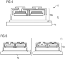
The
Die
Die
Die
Alternativ dazu kann das Konverterelement 5 auch mittels anodischem Bonden auf die epitaktisch gewachsene Schichtenfolge 10b aufgebracht werden. Die Anwendung einer Klebeschicht ist hierbei nicht notwendig.Alternatively, the
Nach einem Verfahrensschritt D) weist der Halbleiterchip 10a eine mechanisch stabile Verbindung mit dem Konverterelement 5 auf, welches vorteilhaft thermisch gut an den Halbleiterchip 10a angebunden ist.After a method step D), the
Die
Es erfolgt ein Anordnen des Halbleiterchips 10a auf einem Hilfsträger 4a (Verfahrensschritt E)), wobei das Konverterelement 5 dem Hilfsträger 4a zugewandt ist, und ein Ablösen des Trägers 4 vom Halbleiterchip 10a (Verfahrensschritt F)). Nach dem Verfahrensschritt E) ist das Konverterelement 5 mechanisch stabil mit dem Hilfsträger 4a verbunden.The
Die Verfahrensschritte D) und E) können vorteilhaft auch gleichzeitig erfolgen.Process steps D) and E) can advantageously also take place simultaneously.
Die
Das Konverterelement kann vorteilhaft den Halbleiterchip und/oder den Waferverbund stabilisieren.The converter element can advantageously stabilize the semiconductor chip and/or the wafer composite.
Das Konverterelement 5 kann vorteilhaft eine ebene Form mit konstanter Dicke umfassen und sich vorteilhaft lateral über die Halbleiterchips 10a oder den Waferverbund hinaus erstrecken. Beispielsweise weist das Konverterelement 5 eine Dicke von größer 100 µm oder größer 200 µm auf. Das Konverterelement 5 weist vorteilhaft eine ebene Oberfläche auf. Das Konverterelement 5 kann auf der Abstrahlseite vorteilhaft eine Aufrauung umfassen. Vor dem Vereinzeln kann das Konverterelement 5 beispielsweise eine in Draufsicht runde Form umfassen. Nach dem Vereinzeln kann sich das Konverterelement 5 in lateraler Richtung wenige um über den Halbleiterchip 10a hinaus erstrecken, beispielsweise an allen Seiten des Halbleiterchips 10a. Das Konverterelement 5 weist vorteilhaft an lateralen Rändern Vereinzelungsspuren auf.The
Ähnlich einer äußeren Verkapselung der Seitenflächen des Halbleiterchips 10a kann auch eine reflektierende Schicht auf die Seitenflächen des Konverterelements aufgebracht werden (nicht gezeigt). Die reflektierende Schicht kann beispielsweise Silber, Aluminium, einen dielektrischen Spiegel oder eine Kombination daraus umfassen.Similar to an external encapsulation of the side surfaces of the
Nach dem Verfahrensschritt F) wird der Waferverbund in eine Vielzahl von Halbleiterchips 10 vereinzelt. Das Vereinzeln erfolgt beispielsweise mittels Laserstrahlschneiden, Stealth Dicing, Plasma Dicing oder mechanischem Sägen, wobei vorteilhaft das Konverterelement 5 und der Hilfsträger 4a zertrennt werden.After method step F), the wafer composite is separated into a large number of
BezugszeichenlisteReference symbol list
- 11
- SaphirsubstratSapphire substrate
- 44
- Trägercarrier
- 4a4a
- HilfsträgerAuxiliary carrier
- 55
- KonverterelementConverter element
- 77
- Klebeschichtadhesive layer
- 1010
- optoelektronisches Bauelementoptoelectronic component
- 10a10a
- lichtemittierender Halbleiterchiplight-emitting semiconductor chip
- 1111
- p-Kontaktstellep-contact point
- 11a11a
- p-dotierter Halbleiterbereichp-doped semiconductor region
- 1212
-
n-Kontaktstelle 12n-
contact point 12 - 12a12a
- n-dotierter Halbleiterbereichn-doped semiconductor region
- 1313
- aktive Zoneactive zone
- 1414
- SpiegelschichtMirror layer
- 14a14a
- KontaktschichtContact layer
- 14b14b
- weitere Kontaktschichtanother contact layer
- 14c14c
- Verkapselungencapsulation
- 1515
- DurchkontaktierungThrough-hole plating
- 15a15a
- KontaktführungContact management
- 1616
- äußere Verkapselungexternal encapsulation
- A)A)
- VerfahrensschrittProcedural step
- B)B)
- VerfahrensschrittProcedural step
- C)C)
- VerfahrensschrittProcedural step
- D)D)
- VerfahrensschrittProcedural step
- E)E)
- VerfahrensschrittProcedural step
- F)F)
- VerfahrensschrittProcedural step
Claims (11)
Applications Claiming Priority (3)
| Application Number | Priority Date | Filing Date | Title |
|---|---|---|---|
| DE102016108682.7A DE102016108682A1 (en) | 2016-05-11 | 2016-05-11 | Method for producing an optoelectronic component and optoelectronic component |
| DE102016108682.7 | 2016-05-11 | ||
| PCT/EP2017/061218 WO2017194623A1 (en) | 2016-05-11 | 2017-05-10 | Method for producing an optoelectronic component, and optoelectronic component |
Publications (2)
| Publication Number | Publication Date |
|---|---|
| DE112017002426A5 DE112017002426A5 (en) | 2019-01-17 |
| DE112017002426B4 true DE112017002426B4 (en) | 2024-02-29 |
Family
ID=58699138
Family Applications (2)
| Application Number | Title | Priority Date | Filing Date |
|---|---|---|---|
| DE102016108682.7A Withdrawn DE102016108682A1 (en) | 2016-05-11 | 2016-05-11 | Method for producing an optoelectronic component and optoelectronic component |
| DE112017002426.9T Active DE112017002426B4 (en) | 2016-05-11 | 2017-05-10 | Method for producing an optoelectronic component and optoelectronic component |
Family Applications Before (1)
| Application Number | Title | Priority Date | Filing Date |
|---|---|---|---|
| DE102016108682.7A Withdrawn DE102016108682A1 (en) | 2016-05-11 | 2016-05-11 | Method for producing an optoelectronic component and optoelectronic component |
Country Status (3)
| Country | Link |
|---|---|
| US (1) | US10854793B2 (en) |
| DE (2) | DE102016108682A1 (en) |
| WO (1) | WO2017194623A1 (en) |
Families Citing this family (9)
| Publication number | Priority date | Publication date | Assignee | Title |
|---|---|---|---|---|
| US11302248B2 (en) | 2019-01-29 | 2022-04-12 | Osram Opto Semiconductors Gmbh | U-led, u-led device, display and method for the same |
| WO2020229576A2 (en) | 2019-05-14 | 2020-11-19 | Osram Opto Semiconductors Gmbh | Illumination unit, method for producing an illumination unit, converter element for an optoelectronic component, radiation source including an led and a converter element, outcoupling structure, and optoelectronic device |
| US11271143B2 (en) | 2019-01-29 | 2022-03-08 | Osram Opto Semiconductors Gmbh | μ-LED, μ-LED device, display and method for the same |
| CN121583214A (en) | 2019-01-29 | 2026-02-27 | 奥斯兰姆奥普托半导体股份有限两合公司 | Video wall, driver circuit, control system and method |
| KR20210120106A (en) | 2019-02-11 | 2021-10-06 | 오스람 옵토 세미컨덕터스 게엠베하 | Optoelectronic Components, Optoelectronic Assemblies and Methods |
| US11538852B2 (en) | 2019-04-23 | 2022-12-27 | Osram Opto Semiconductors Gmbh | μ-LED, μ-LED device, display and method for the same |
| JP7604394B2 (en) * | 2019-04-23 | 2024-12-23 | エイエムエス-オスラム インターナショナル ゲーエムベーハー | LED module, LED display module, and method for manufacturing said module |
| WO2020233873A1 (en) | 2019-05-23 | 2020-11-26 | Osram Opto Semiconductors Gmbh | Lighting arrangement, light guiding arrangement and method |
| CN114730824A (en) | 2019-09-20 | 2022-07-08 | 奥斯兰姆奥普托半导体股份有限两合公司 | Optoelectronic component, semiconductor structure and method |
Citations (4)
| Publication number | Priority date | Publication date | Assignee | Title |
|---|---|---|---|---|
| JP2005327820A (en) * | 2004-05-12 | 2005-11-24 | Matsushita Electric Works Ltd | Light emitting diode package, light emitting device using the same, and method for manufacturing the light emitting device |
| DE102008039790A1 (en) * | 2008-08-26 | 2010-03-04 | Osram Opto Semiconductors Gmbh | Optoelectronic component i.e. LED, for use as headlight in motor vehicle, has connecting terminals provided for supplying charge carriers to partial layers of layer sequence, where terminals are arranged at main side of layer sequence |
| US20120074441A1 (en) * | 2010-09-24 | 2012-03-29 | Seoul Semiconductor Co., Ltd. | Wafer-level light emitting diode package and method of fabricating the same |
| DE102012217776A1 (en) * | 2012-09-28 | 2014-06-12 | Osram Opto Semiconductors Gmbh | Method for producing an optoelectronic component |
Family Cites Families (6)
| Publication number | Priority date | Publication date | Assignee | Title |
|---|---|---|---|---|
| DE102009051746A1 (en) * | 2009-09-30 | 2011-03-31 | Osram Opto Semiconductors Gmbh | Optoelectronic component |
| US8232117B2 (en) | 2010-04-30 | 2012-07-31 | Koninklijke Philips Electronics N.V. | LED wafer with laminated phosphor layer |
| CZ201188A3 (en) | 2011-02-17 | 2013-02-20 | Crytur Spol. S R. O. | Preparation of doped garnet structure single crystals with diameters of up to 500 mm |
| DE102014100772B4 (en) | 2014-01-23 | 2022-11-03 | OSRAM Opto Semiconductors Gesellschaft mit beschränkter Haftung | Method for producing optoelectronic semiconductor components and optoelectronic semiconductor component |
| DE102014102292A1 (en) | 2014-02-21 | 2015-08-27 | Osram Opto Semiconductors Gmbh | Method for producing an optoelectronic component |
| DE102015109413A1 (en) * | 2015-06-12 | 2016-12-15 | Osram Opto Semiconductors Gmbh | Process for the production of optoelectronic conversion semiconductor chips and combination of conversion semiconductor chips |
-
2016
- 2016-05-11 DE DE102016108682.7A patent/DE102016108682A1/en not_active Withdrawn
-
2017
- 2017-05-10 DE DE112017002426.9T patent/DE112017002426B4/en active Active
- 2017-05-10 US US16/098,172 patent/US10854793B2/en active Active
- 2017-05-10 WO PCT/EP2017/061218 patent/WO2017194623A1/en not_active Ceased
Patent Citations (4)
| Publication number | Priority date | Publication date | Assignee | Title |
|---|---|---|---|---|
| JP2005327820A (en) * | 2004-05-12 | 2005-11-24 | Matsushita Electric Works Ltd | Light emitting diode package, light emitting device using the same, and method for manufacturing the light emitting device |
| DE102008039790A1 (en) * | 2008-08-26 | 2010-03-04 | Osram Opto Semiconductors Gmbh | Optoelectronic component i.e. LED, for use as headlight in motor vehicle, has connecting terminals provided for supplying charge carriers to partial layers of layer sequence, where terminals are arranged at main side of layer sequence |
| US20120074441A1 (en) * | 2010-09-24 | 2012-03-29 | Seoul Semiconductor Co., Ltd. | Wafer-level light emitting diode package and method of fabricating the same |
| DE102012217776A1 (en) * | 2012-09-28 | 2014-06-12 | Osram Opto Semiconductors Gmbh | Method for producing an optoelectronic component |
Also Published As
| Publication number | Publication date |
|---|---|
| DE112017002426A5 (en) | 2019-01-17 |
| DE102016108682A1 (en) | 2017-11-16 |
| US10854793B2 (en) | 2020-12-01 |
| US20190148606A1 (en) | 2019-05-16 |
| WO2017194623A1 (en) | 2017-11-16 |
Similar Documents
| Publication | Publication Date | Title |
|---|---|---|
| DE112017002426B4 (en) | Method for producing an optoelectronic component and optoelectronic component | |
| EP1920470B1 (en) | Method for manufacturing a surface-mounted optoelectronic semiconductor device | |
| DE10204386B4 (en) | Light emitting diode and process for its manufacture | |
| DE112015002479B4 (en) | Semiconductor component and lighting device | |
| EP2483937B1 (en) | Optoelectronic component | |
| DE102015114849A1 (en) | Method for producing light-emitting diode filaments and light-emitting filament | |
| DE102012102847A1 (en) | A light-emitting semiconductor component and method for producing a light-emitting semiconductor component | |
| WO2008131736A1 (en) | Optoelectronic component and method for producing a plurality of optoelectronic components | |
| WO2009003435A1 (en) | Method for producing optoelectronic components, and optoelectronic component | |
| DE102007030129A1 (en) | Method for producing a plurality of optoelectronic components and optoelectronic component | |
| EP1774599B1 (en) | Method for producing semiconductor chips using thin-film technology and a semiconductor chip produced using thin-film technology | |
| DE102014100773A1 (en) | Semiconductor device and method for manufacturing a semiconductor device | |
| WO2014048830A1 (en) | Optoelectronic component | |
| WO2009039816A1 (en) | Radiation-emitting component having glass cover and method for the production thereof | |
| DE112015005127B4 (en) | Optoelectronic semiconductor component and method for producing an optoelectronic semiconductor component | |
| WO2015010997A1 (en) | Surface-mountable optoelectronic semiconductor component and method for producing at least one surface-mountable optoelectronic semiconductor component | |
| DE112019005876B4 (en) | LIGHT-EMITTING COMPONENT AND METHOD FOR PRODUCING A LIGHT-EMITTING COMPONENT | |
| DE102010009455B4 (en) | Semiconductor laser device with a semiconductor laser chip and method for the production thereof | |
| DE102017104479B4 (en) | Process for the production of optoelectronic semiconductor components | |
| WO2013131729A1 (en) | Method for producing an optoelectronic semiconductor chip | |
| WO2009121314A1 (en) | Radiation-emitting semi-conductor component and method for producing a radiation-emitting semi-conductor component | |
| DE102008028886A1 (en) | Radiation-emitting component and method for producing a radiation-emitting component | |
| DE102017104144B4 (en) | Process for the production of light emitting diodes | |
| WO2018202685A1 (en) | Optoelectronic semiconductor chip and method for producing an optoelectronic semiconductor chip | |
| DE102019131502A1 (en) | METHOD FOR MANUFACTURING RADIATION-EMITTING SEMICONDUCTOR CHIPS, RADIATION-EMITTING SEMICONDUCTOR CHIP AND RADIATION-EMITTING COMPONENT |
Legal Events
| Date | Code | Title | Description |
|---|---|---|---|
| R012 | Request for examination validly filed | ||
| R079 | Amendment of ipc main class |
Free format text: PREVIOUS MAIN CLASS: H01L0033000000 Ipc: H01L0033500000 |
|
| R016 | Response to examination communication | ||
| R018 | Grant decision by examination section/examining division | ||
| R079 | Amendment of ipc main class |
Free format text: PREVIOUS MAIN CLASS: H01L0033500000 Ipc: H10H0020851000 |
|
| R020 | Patent grant now final |