DE112016006354B4 - SILICON WAFER SINGLE SIDE POLISHING PROCESS - Google Patents
SILICON WAFER SINGLE SIDE POLISHING PROCESS Download PDFInfo
- Publication number
- DE112016006354B4 DE112016006354B4 DE112016006354.7T DE112016006354T DE112016006354B4 DE 112016006354 B4 DE112016006354 B4 DE 112016006354B4 DE 112016006354 T DE112016006354 T DE 112016006354T DE 112016006354 B4 DE112016006354 B4 DE 112016006354B4
- Authority
- DE
- Germany
- Prior art keywords
- polishing
- silicon wafer
- silicon
- condition
- polishing rate
- Prior art date
- Legal status (The legal status is an assumption and is not a legal conclusion. Google has not performed a legal analysis and makes no representation as to the accuracy of the status listed.)
- Active
Links
Images



Classifications
-
- B—PERFORMING OPERATIONS; TRANSPORTING
- B24—GRINDING; POLISHING
- B24B—MACHINES, DEVICES, OR PROCESSES FOR GRINDING OR POLISHING; DRESSING OR CONDITIONING OF ABRADING SURFACES; FEEDING OF GRINDING, POLISHING, OR LAPPING AGENTS
- B24B37/00—Lapping machines or devices; Accessories
- B24B37/04—Lapping machines or devices; Accessories designed for working plane surfaces
- B24B37/07—Lapping machines or devices; Accessories designed for working plane surfaces characterised by the movement of the work or lapping tool
- B24B37/10—Lapping machines or devices; Accessories designed for working plane surfaces characterised by the movement of the work or lapping tool for single side lapping
- B24B37/105—Lapping machines or devices; Accessories designed for working plane surfaces characterised by the movement of the work or lapping tool for single side lapping the workpieces or work carriers being actively moved by a drive, e.g. in a combined rotary and translatory movement
- B24B37/107—Lapping machines or devices; Accessories designed for working plane surfaces characterised by the movement of the work or lapping tool for single side lapping the workpieces or work carriers being actively moved by a drive, e.g. in a combined rotary and translatory movement in a rotary movement only, about an axis being stationary during lapping
-
- H—ELECTRICITY
- H10—SEMICONDUCTOR DEVICES; ELECTRIC SOLID-STATE DEVICES NOT OTHERWISE PROVIDED FOR
- H10P—GENERIC PROCESSES OR APPARATUS FOR THE MANUFACTURE OR TREATMENT OF DEVICES COVERED BY CLASS H10
- H10P52/00—Grinding, lapping or polishing of wafers, substrates or parts of devices
-
- B—PERFORMING OPERATIONS; TRANSPORTING
- B24—GRINDING; POLISHING
- B24B—MACHINES, DEVICES, OR PROCESSES FOR GRINDING OR POLISHING; DRESSING OR CONDITIONING OF ABRADING SURFACES; FEEDING OF GRINDING, POLISHING, OR LAPPING AGENTS
- B24B37/00—Lapping machines or devices; Accessories
- B24B37/04—Lapping machines or devices; Accessories designed for working plane surfaces
- B24B37/042—Lapping machines or devices; Accessories designed for working plane surfaces operating processes therefor
-
- B—PERFORMING OPERATIONS; TRANSPORTING
- B24—GRINDING; POLISHING
- B24B—MACHINES, DEVICES, OR PROCESSES FOR GRINDING OR POLISHING; DRESSING OR CONDITIONING OF ABRADING SURFACES; FEEDING OF GRINDING, POLISHING, OR LAPPING AGENTS
- B24B37/00—Lapping machines or devices; Accessories
- B24B37/04—Lapping machines or devices; Accessories designed for working plane surfaces
- B24B37/07—Lapping machines or devices; Accessories designed for working plane surfaces characterised by the movement of the work or lapping tool
- B24B37/10—Lapping machines or devices; Accessories designed for working plane surfaces characterised by the movement of the work or lapping tool for single side lapping
-
- B—PERFORMING OPERATIONS; TRANSPORTING
- B24—GRINDING; POLISHING
- B24B—MACHINES, DEVICES, OR PROCESSES FOR GRINDING OR POLISHING; DRESSING OR CONDITIONING OF ABRADING SURFACES; FEEDING OF GRINDING, POLISHING, OR LAPPING AGENTS
- B24B37/00—Lapping machines or devices; Accessories
- B24B37/04—Lapping machines or devices; Accessories designed for working plane surfaces
- B24B37/07—Lapping machines or devices; Accessories designed for working plane surfaces characterised by the movement of the work or lapping tool
- B24B37/10—Lapping machines or devices; Accessories designed for working plane surfaces characterised by the movement of the work or lapping tool for single side lapping
- B24B37/105—Lapping machines or devices; Accessories designed for working plane surfaces characterised by the movement of the work or lapping tool for single side lapping the workpieces or work carriers being actively moved by a drive, e.g. in a combined rotary and translatory movement
-
- B—PERFORMING OPERATIONS; TRANSPORTING
- B24—GRINDING; POLISHING
- B24B—MACHINES, DEVICES, OR PROCESSES FOR GRINDING OR POLISHING; DRESSING OR CONDITIONING OF ABRADING SURFACES; FEEDING OF GRINDING, POLISHING, OR LAPPING AGENTS
- B24B51/00—Arrangements for automatic control of a series of individual steps in grinding a workpiece
-
- H—ELECTRICITY
- H10—SEMICONDUCTOR DEVICES; ELECTRIC SOLID-STATE DEVICES NOT OTHERWISE PROVIDED FOR
- H10P—GENERIC PROCESSES OR APPARATUS FOR THE MANUFACTURE OR TREATMENT OF DEVICES COVERED BY CLASS H10
- H10P52/00—Grinding, lapping or polishing of wafers, substrates or parts of devices
- H10P52/40—Chemomechanical polishing [CMP]
- H10P52/402—Chemomechanical polishing [CMP] of semiconductor materials
-
- H—ELECTRICITY
- H10—SEMICONDUCTOR DEVICES; ELECTRIC SOLID-STATE DEVICES NOT OTHERWISE PROVIDED FOR
- H10P—GENERIC PROCESSES OR APPARATUS FOR THE MANUFACTURE OR TREATMENT OF DEVICES COVERED BY CLASS H10
- H10P90/00—Preparation of wafers not covered by a single main group of this subclass, e.g. wafer reinforcement
- H10P90/12—Preparing bulk and homogeneous wafers
- H10P90/129—Preparing bulk and homogeneous wafers by polishing
-
- H—ELECTRICITY
- H10—SEMICONDUCTOR DEVICES; ELECTRIC SOLID-STATE DEVICES NOT OTHERWISE PROVIDED FOR
- H10P—GENERIC PROCESSES OR APPARATUS FOR THE MANUFACTURE OR TREATMENT OF DEVICES COVERED BY CLASS H10
- H10P95/00—Generic processes or apparatus for manufacture or treatments not covered by the other groups of this subclass
- H10P95/04—Planarisation of conductive or resistive materials
-
- H—ELECTRICITY
- H10—SEMICONDUCTOR DEVICES; ELECTRIC SOLID-STATE DEVICES NOT OTHERWISE PROVIDED FOR
- H10P—GENERIC PROCESSES OR APPARATUS FOR THE MANUFACTURE OR TREATMENT OF DEVICES COVERED BY CLASS H10
- H10P95/00—Generic processes or apparatus for manufacture or treatments not covered by the other groups of this subclass
- H10P95/06—Planarisation of inorganic insulating materials
-
- H—ELECTRICITY
- H10—SEMICONDUCTOR DEVICES; ELECTRIC SOLID-STATE DEVICES NOT OTHERWISE PROVIDED FOR
- H10P—GENERIC PROCESSES OR APPARATUS FOR THE MANUFACTURE OR TREATMENT OF DEVICES COVERED BY CLASS H10
- H10P95/00—Generic processes or apparatus for manufacture or treatments not covered by the other groups of this subclass
- H10P95/06—Planarisation of inorganic insulating materials
- H10P95/062—Planarisation of inorganic insulating materials involving a dielectric removal step
-
- B—PERFORMING OPERATIONS; TRANSPORTING
- B24—GRINDING; POLISHING
- B24B—MACHINES, DEVICES, OR PROCESSES FOR GRINDING OR POLISHING; DRESSING OR CONDITIONING OF ABRADING SURFACES; FEEDING OF GRINDING, POLISHING, OR LAPPING AGENTS
- B24B37/00—Lapping machines or devices; Accessories
- B24B37/005—Control means for lapping machines or devices
- B24B37/0053—Control means for lapping machines or devices detecting loss or breakage of a workpiece during lapping
Landscapes
- Engineering & Computer Science (AREA)
- Mechanical Engineering (AREA)
- Mechanical Treatment Of Semiconductor (AREA)
- Finish Polishing, Edge Sharpening, And Grinding By Specific Grinding Devices (AREA)
Abstract
Siliziumwafer-Einseiten-Polierverfahren des Haltens, durch einen Polierkopf, eines Siliziumwafers, in dem eine Siliziumoxidschicht auf einer blanken Siliziumoberfläche ausgebildet ist, und des Drückens des Siliziumwafers gegen eine rotierbare Scheibe mit einem daran angebrachten Poliertuch unter Drehen des Siliziumwafers, um eine Seite des Siliziumwafers, die der drehbaren Scheibe zugewandt ist, zu polieren, wobei das Siliziumwafer-Einseiten-Polierverfahren Folgendes umfasst:
einen ersten Polierschritt des Durchführens des Polierens auf der einen Seite des Siliziumwafers unter einer ersten Polierbedingung bezüglich eines aufgebrachten Drucks zum Drücken des Siliziumwafers und einer relativen Geschwindigkeit des Siliziumwafers und der drehbaren Platte; und
einen zweiten Polierschritt des Durchführens des Polierens auf der einen Seite des Siliziumwafers unter einer zweiten Polierbedingung, bei der der aufgebrachte Druck und/oder die relative Geschwindigkeit der ersten Polierbedingung geändert ist, nach dem ersten Polierschritt,
wobei ein Polierratenverhältnis einer Siliziumoxidpolierrate zu einer Siliziumpolierrate gemäß der ersten Polierbedingung über einem Polierratenverhältnis einer Siliziumoxidpolierrate zu einer Siliziumpolierrate gemäß der zweiten Polierbedingung liegt.

a first polishing step of performing polishing on one side of the silicon wafer under a first polishing condition with respect to an applied pressure for pressing the silicon wafer and a relative speed of the silicon wafer and the rotatable plate; and
a second polishing step of performing polishing on one side of the silicon wafer under a second polishing condition in which the applied pressure and/or the relative speed of the first polishing condition is changed after the first polishing step,
wherein a polishing rate ratio of a silicon oxide polishing rate to a silicon polishing rate according to the first polishing condition is above a polishing rate ratio of a silicon oxide polishing rate to a silicon polishing rate according to the second polishing condition.
Description
ERFINDUNGSGEBIETFIELD OF THE INVENTION
Die vorliegende Offenbarung betrifft ein Siliziumwafer-Einseiten-Polierverfahren.The present disclosure relates to a silicon wafer single-side polishing process.
ALLGEMEINER STAND DER TECHNIKGENERAL STATE OF THE ART
Verfahren zum Polieren von Oberflächen von Halbleiterwafern, die höchst eben sein müssen, wie etwa von Siliziumwafern, werden grob in zwei Arten eingeteilt: ein Doppelseiten-Polierverfahren des gleichzeitigen Polierens von beiden Seiten eines Halbleiterwafers; und ein Einseiten-Polierverfahrens des Polierens nur einer Seite davon. Einseiten-Polierverfahren werden in einer großen Vielzahl von Anwendungen vom Läppen unter Verwendung eines relativ steifen Poliertuchs bis zum Endpolieren unter Verwendung eines relativ weichen Poliertuchs verwendet.Methods for polishing surfaces of semiconductor wafers that must be highly flat, such as silicon wafers, are broadly classified into two types: a double-side polishing method of simultaneously polishing both sides of a semiconductor wafer; and a one-side polishing method of polishing only one side thereof. Single-side polishing processes are used in a wide variety of applications from lapping using a relatively stiff polishing cloth to final polishing using a relatively soft polishing cloth.
Ein typisches Einseiten-Polierverfahren unter Verwendung einer herkömmlichen Einseiten-Poliervorrichtung 100 wird unten unter Bezugnahme auf
QUELLENANGABESOURCE
PatentliteraturenPatent literature
PTL 1:
KURZDARSTELLUNGSHORT PRESENTATION
(Technisches Problem)(Technical problem)
Durch Einseitenpolieren kann eine ebene Oberfläche mit einem gewissen Grad an hoher Ebenheit ausgebildet werden, und die Oberflächenrauigkeit kann reduziert werden. Eine Polierungleichmäßigkeit in der Halbleiteroberfläche ist jedoch unvermeidbar, und es ist schwierig, eine vollständig ebene Oberfläche in der nm-Größenordnung auszubilden. Das gleiche gilt für den Fall, in dem ein Siliziumwafer einem Einseitenpolieren unterzogen wird. Dementsprechend wird die Qualität der Siliziumwaferoberfläche nach dem Endpolieren unter Verwendung verschiedener Indizes evaluiert, und jeder Siliziumwafer, der vorbestimmten Bedingungen genügt, wird als ein normgerechter Gegenstand behandelt.By single-side polishing, a flat surface with a certain degree of high flatness can be formed, and the surface roughness can be reduced. However, polishing unevenness in the semiconductor surface is unavoidable, and it is difficult to form a completely flat surface in the nm order. The same applies to the case where a silicon wafer is subjected to one-side polishing. Accordingly, the quality of the silicon wafer surface after final polishing is evaluated using various indices, and each silicon wafer satisfying predetermined conditions is treated as a standard article.
In den vergangenen Jahren ist zunehmend eine Qualitätsevaluierung von Siliziumwaferoberflächen nach dem Endpolieren unter Verwendung des Differenzialinterferenzkontrast(DIC - Differential Interference Contrast)-Verfahrens zunehmend eingesetzt worden. Im Detail wird die Anzahl von konkav-konvex-förmigen abgestuften winzigen Defekten mit einer Höhe (oder Tiefe), die einen vorbestimmten Schwellenwert übersteigt, durch das DIC-Verfahren detektiert, und die Qualität der Siliziumwaferoberfläche wird evaluiert. Die Breite eines abgestuften winzigen Defekts beträgt üblicherweise 30 µm bis 100 µm, und die Differenz in der Höhe ist sehr klein.In recent years, quality evaluation of silicon wafer surfaces after final polishing using the Differential Interference Contrast (DIC) method has become increasingly common. In detail, the number of concavo-convex-shaped graded minute defects with a height (or depth) exceeding a predetermined threshold is detected by the DIC method, and the quality of the silicon wafer surface is evaluated. The width of a graded tiny defect is usually 30 µm to 100 µm, and the difference in height is very small.
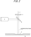
In dem DIC-Verfahren wird ein Laser L (z.B. He-Ne-Laser) durch einen Strahlteiler S aufgeteilt und auf die Oberfläche des Halbleiterwafers W gerichtet, wie in
Falls die Anzahl an abgestuften winzigen Defekten innerhalb einer gewünschten Anforderung liegt, kann die Qualität der Siliziumwaferoberfläche nach dem Endpolieren als gut bestimmt werden. Dabei wird jeder Siliziumwafer, der der gewünschten Anforderung nicht genügt, als ein nicht normgerechter Gegenstand bestimmt und kann somit nicht als ein Produkt versandt werden.If the number of graded minute defects is within a desired requirement, the quality of the silicon wafer surface after final polishing can be determined to be good. Any silicon wafer that does not meet the desired requirements is determined to be a non-standard item and therefore cannot be shipped as a product.
Mit herkömmlichen Einseiten-Polierverfahren liegt die Häufigkeit von abgestuften winzigen Defekten in der Siliziumwaferoberfläche nach dem Endpolieren nicht notwendigerweise auf einer zufriedenstellenden Höhe. Um die Produktausbeute zu verbessern, wird ein verbessertes Einseiten-Polierverfahren benötigt.With conventional single-side polishing methods, the frequency of graded minute defects in the silicon wafer surface after final polishing is not necessarily at a satisfactory level. To improve product yield, an improved single-side polishing process is needed.
Es könnte deshalb hilfreich sein, ein Siliziumwafer-Einseiten-Polierverfahren bereitzustellen, das die Häufigkeit für abgestufte winzige Effekte signifikant verbessern kann.It might therefore be helpful to provide a silicon wafer single-side polishing process that can significantly improve the frequency for graded minute effects.
(Lösung des Problems)(The solution of the problem)
Wir haben ausführliche Forschung zur Lösung des oben erwähnten Problems durchgeführt und uns folgende Idee ausgedacht. Zuerst befindet sich der Siliziumwafer, wenn ein finales Polieren an einem Siliziumwafer durchgeführt wird, in einem natürlich oxidierten Zustand. Im Detail besteht der Siliziumwafer aus blankem Silizium (Abschnitt ohne natürliche Oxidschicht) und einer Siliziumoxidschicht (die typischerweise eine natürliche Oxidschicht ist), die die Oberfläche des blanken Siliziums bedeckt. In diesem Zustand wird das Einseitenpolieren des Siliziumwafers gestartet. Mit Einseiten-Polierverfahren ist es schwierig, eine Polierungleichmäßigkeit in der Siliziumwaferoberfläche vollständig zu verhindern, und es tritt der Augenblick auf, zu dem ein Abschnitt, wo die Siliziumoxidschicht polierend entfernt wird, und ein Abschnitt, wo die Siliziumoxidschicht zurückbleibt, zusammen existieren (siehe Schritt 4B in
Bei Einseiten-Polierverfahren trägt, obwohl das Polieren der Entfernung der Siliziumoxidschicht durch chemisch-mechanisches Polieren durchgeführt wird, zu dem polierenden Entfernen des größten Teils der Siliziumoxidschicht das mechanische Polieren bei. Dabei trägt zu dem Polieren des blanken Siliziums sowohl chemisches Polieren als auch mechanisches Polieren bei. Somit liegt bei dem Einseitenpolieren des Siliziumwafers die Polierrate des Siliziumoxids typischerweise unter der Polierrate des Siliziums. Nach dem Auftreten des oben erwähnten Koexistenzzustands schreitet, während das polierende Entfernen des verbleibendie Siliziumoxidschichts weitergeht, das Polieren des blanken Siliziums in dem Abschnitt schnell weiter, wo die Siliziumoxidschicht bereits polierend entfernt worden ist. Dieser Abschnitt wird schließlich einen abgestuften winzigen Defekt besitzen.In single-side polishing methods, although the polishing removal of the silicon oxide layer is carried out by chemical mechanical polishing, mechanical polishing contributes to the polishing removal of most of the silicon oxide layer. Both chemical polishing and mechanical polishing contribute to the polishing of the bare silicon. Thus, when polishing the silicon wafer on one side, the polishing rate of the silicon oxide is typically lower than the polishing rate of the silicon. After the occurrence of the above-mentioned coexistence state, while the polishing removal of the remaining silicon oxide layer continues, the polishing of the bare silicon proceeds rapidly in the portion where the silicon oxide layer has already been polishingly removed. This section will eventually have a stepped tiny defect.
Wir haben dann das Durchführen eines Einseitenpolierens mit einer Bedingung einer erhöhten Siliziumoxidpolierrate in Betracht gezogen. Da jedoch der Beitrag des mechanischen Polierens dominant ist, nimmt in diesem Fall jedoch nicht nur die Polierrate des blanken Siliziums ab, sondern es ist auch wahrscheinlich, dass das polierende Durchhängen in dem peripheren Teil des Siliziumwafers zunimmt. Dem ist so, weil eine Bedingung einer erhöhten Siliziumoxidpolierrate eine Polierbedingung ist, gemäß der der Beitrag der mechanischen Polierwirkung dominant ist, und deshalb nimmt der Beitrag der chemischen Polierwirkung ab. Wir haben dann entdeckt, dass die Häufigkeit von abgestuften winzigen Defekten signifikant verbessert werden kann, indem zuerst ein Polieren durchgeführt wird, das für das polierende Entfernen der Siliziumoxidschicht bestimmt ist, und dann das Polieren durchgeführt wird, das für das Endpolieren des Siliziums bestimmt ist. Somit stellen wir Folgendes bereit.We then considered performing single-side polishing with an increased silica polishing rate condition. However, in this case, since the contribution of mechanical polishing is dominant, not only the polishing rate of the bare silicon decreases, but also the polishing slack in the peripheral part of the silicon wafer is likely to increase. This is because a condition of increased silica polishing rate is a polishing condition according to which the contribution of the mechanical polishing action is dominant, and therefore the contribution of the chemical polishing action decreases. We then discovered that the frequency of graded minute defects can be significantly improved by first performing polishing intended for polishing removal of the silicon oxide layer and then performing polishing intended for final polishing of the silicon. Thus, we provide the following.
Ein Siliziumwafer-Einseiten-Polierverfahren gemäß der vorliegenden Offenbarung ist ein Siliziumwafer-Einseiten-Polierverfahren des Haltens, durch einen Polierkopf, eines Siliziumwafers, bei dem eine Siliziumoxidschicht auf einer blanken Siliziumoberfläche ausgebildet ist, und des Drückens des Siliziumwafers gegen eine rotierbare Scheibe mit einem daran angebrachten Poliertuch unter Drehen des Siliziumwafers, um eine Seite des Siliziumwafers, die der drehbaren Scheibe zugewandt ist, zu polieren, wobei das Siliziumwafer-Einseiten-Polierverfahren Folgendes umfasst: einen ersten Polierschritt des Durchführens des Polierens auf der einen Seite des Siliziumwafers unter einer ersten Polierbedingung bezüglich eines aufgebrachten Drucks zum Drücken des Siliziumwafers und einer relativen Geschwindigkeit des Siliziumwafers und der drehbaren Platte; und einen zweiten Polierschritt des Durchführens des Polierens auf der einen Seite des Siliziumwafers unter einer zweiten Polierbedingung, bei der der aufgebrachte Druck und/oder die relative Geschwindigkeit in der ersten Polierbedingung geändert ist, nach dem ersten Polierschritt, wobei ein Polierratenverhältnis einer Siliziumoxidpolierrate zu einer Siliziumpolierrate gemäß der ersten Polierbedingung über einem Polierratenverhältnis einer Siliziumoxidpolierrate zu einer Siliziumpolierrate gemäß der zweiten Polierbedingung liegt.A silicon wafer single-side polishing method according to the present disclosure is a silicon wafer single-side polishing method of holding, by a polishing head, a silicon wafer having a silicon oxide layer formed on a bare silicon surface, and pressing the silicon wafer against a rotatable disk having a thereon attached polishing cloth while rotating the silicon wafer to polish a side of the silicon wafer facing the rotatable disk, the silicon wafer one-side polishing method comprising: a first polishing step of performing polishing on the one side of the silicon wafer under a first polishing condition with respect to an applied pressure for pressing the silicon wafer and a relative speed of the silicon wafer and the rotatable plate; and a second polishing step of performing polishing on one side of the Silicon wafer under a second polishing condition in which the applied pressure and/or the relative speed in the first polishing condition is changed after the first polishing step, wherein a polishing rate ratio of a silicon oxide polishing rate to a silicon polishing rate according to the first polishing condition over a polishing rate ratio of a silicon oxide polishing rate to a silicon polishing rate according to the second polishing condition.
Bevorzugt wird der erste Polierschritt durchgeführt, bis mindestens die Siliziumoxidschicht entfernt ist.The first polishing step is preferably carried out until at least the silicon oxide layer is removed.
Bevorzugt beträgt das Polierratenverhältnis gemäß der ersten Polierbedingung 0,5 oder mehr. Bevorzugt liegt das Polierratenverhältnis gemäß der zweiten Polierbedingung unter 0,5.Preferably, the polishing rate ratio according to the first polishing condition is 0.5 or more. Preferably, the polishing rate ratio according to the second polishing condition is below 0.5.
(Vorteilhafter Effekt)(Beneficial effect)
Gemäß der vorliegenden Offenbarung werden der ersten Polierschritt und der zweite Polierschritt unter den jeweiligen Polierbedingungen durchgeführt, die hinsichtlich des Polierratenverhältnisses der Siliziumoxidpolierrate zu der Siliziumpolierrate differieren. Es ist somit möglich, ein Siliziumwafer-Einseiten-Polierverfahren bereitzustellen, das die Häufigkeit von abgestuften winzigen Effekten signifikant verbessern kann.According to the present disclosure, the first polishing step and the second polishing step are performed under the respective polishing conditions that differ in the polishing rate ratio of the silicon oxide polishing rate to the silicon polishing rate. It is thus possible to provide a silicon wafer single-side polishing method that can significantly improve the frequency of graded minute effects.
KURZE BESCHREIBUNG DER ZEICHNUNGENBRIEF DESCRIPTION OF THE DRAWINGS
In den beiliegenden Zeichnungen zeigen:
-
1 ein Schemadiagramm, das ein herkömmliches Halbleiterwafer-Einseiten-Polierverfahren darstellt; -
2 ein Schemadiagramm, das das Messprinzip für abgestufte winzige Defekte durch das Differenzialinterferenzkontrastverfahren gemäß einer herkömmlichen Technik darstellt; -
3 ein schematisches Schnittdiagramm, das einen Polierprozess durch ein Einseiten-Polierverfahren gemäß einer der offenbarten Ausführungsformen darstellt; -
4 ein schematisches Schnittdiagramm, das einen Polierprozess durch ein herkömmliches Einseiten-Polierverfahren darstellt; -
5A eine graphische Darstellung, die ein Beispiel für die jeweiligen Polierraten von Silizium und Siliziumoxid gegen den aufgebrachten Druck gemäß einer der offenbarten Ausführungsformen darstellt; -
5B eine graphische Darstellung, die ein Beispiel für die jeweiligen Polierraten von Silizium und Siliziumoxid gegen die relative Geschwindigkeit gemäß einer der offenbarten Ausführungsformen darstellt; -
6 eine graphische Darstellung, die die Anzahl von abgestuften winzigen Defekten mit der Siliziumpolierrate und der Siliziumoxidpolierrate gemäß einer der offenbarten Ausführungsformen darstellt; und -
7 eine graphische Darstellung, die das in einem vorausgehenden Versuchsbeispiel gemessene Polierratenverhältnis darstellt.
-
1 a schematic diagram illustrating a conventional semiconductor wafer single-side polishing process; -
2 a schematic diagram illustrating the measuring principle for graded minute defects by the differential interference contrast method according to a conventional technique; -
3 a schematic sectional diagram illustrating a polishing process by a single-side polishing method according to one of the disclosed embodiments; -
4 a schematic sectional diagram illustrating a polishing process by a conventional single-side polishing method; -
5A is a graph illustrating an example of the respective polishing rates of silicon and silicon oxide versus applied pressure in accordance with one of the disclosed embodiments; -
5B is a graph illustrating an example of the respective polishing rates of silicon and silicon oxide versus relative speed in accordance with one of the disclosed embodiments; -
6 a graph illustrating the number of graded minute defects with the silicon polishing rate and the silicon oxide polishing rate according to one of the disclosed embodiments; and -
7 a graph showing the polishing rate ratio measured in a previous experimental example.
AUSFÜHRLICHE BESCHREIBUNGDETAILED DESCRIPTION
Eine der offenbarten Ausführungsformen wird unten unter Bezugnahme auf Zeichnungen beschrieben. In den
(Einseiten-Polierverfahren)(Single-side polishing process)
Ein Siliziumwafer-Einseiten-Polierverfahren gemäß einer der offenbarten Ausführungsformen wird unten unter Bezugnahme auf die
Dieses Einseitenpolieren kann gemäß eines üblichen Verfahrens unter Verwendung einer typischen Einseiten-Polierverfahren durchgeführt werden. Unter Bezugnahme auf die oben erwähnte
Das Einseiten-Polierverfahren gemäß dieser Ausführungsform beinhaltet: einen ersten Polierschritt des Durchführens des Polierens auf der einen Seite des Siliziumwafers W unter einer ersten Polierbedingung bezüglich des aufgebrachten Drucks zum Drücken des Siliziumwafers W und einer relativen Geschwindigkeit des Siliziumwafers W und der drehbaren Platte (Schritt 3A und Schritt 3B von
In dieser Ausführungsform ist wichtig, dass das Polierratenverhältnis (im Folgenden als „SiO2/Si-Polierratenverhältnis“ bezeichnet) der SiO2-Polierrate zu der Si-Polierrate gemäß der ersten Polierbedingung über dem SiO2/Si-Polierratenverhältnis gemäß der nachfolgenden zweiten Polierbedingung liegt. Durch diese Schritte kann die Häufigkeit von abgestuften winzigen Defekten in der Siliziumwaferoberfläche nach dem Polieren signifikant verbessert werden. Jeder Schritt wird unten beschrieben.What is important in this embodiment is that the polishing rate ratio (hereinafter referred to as “SiO 2 /Si polishing rate ratio”) of the SiO 2 polishing rate to the Si polishing rate according to the first polishing condition is over the SiO 2 /Si polishing rate ratio according to the subsequent second polishing condition lies. These steps can significantly improve the frequency of graded tiny defects in the silicon wafer surface after polishing. Each step is described below.
In dem ersten Polierschritt (Schritt 3A und Schritt 3B von
Die erste Polierbedingung enthält möglicherweise nicht nur den oben erwähnten aufgebrachten Druck und die oben erwähnte relative Geschwindigkeit, sondern auch den Aufschlämmungs(Slurry)-Typ (Partikeldurchmesser, Konzentration, pH-Wert usw.) und die Zuführtemperatur, das Material, den Porendurchmesser und das Öffnungsverhältnis usw. des Poliertuchs und dergleichen. Die zweite Polierbedingung enthält möglicherweise nicht nur den aufgebrachten Druck und die relative Geschwindigkeit, sondern auch den Aufschlämmungstyp und die Zuführtemperatur, das Material, den Porendurchmesser und das Öffnungsverhältnis des Poliertuchs und dergleichen als Polierbedingungen, wie bei der ersten Polierbedingung.The first polishing condition may include not only the above-mentioned applied pressure and relative velocity, but also the slurry type (particle diameter, concentration, pH, etc.) and feed temperature, material, pore diameter, and so on Aperture ratio etc. of the polishing cloth and the like. The second polishing condition may include not only the applied pressure and the relative speed but also the slurry type and feed temperature, the material, the pore diameter and the opening ratio of the polishing cloth and the like as polishing conditions as in the first polishing condition.
In dem zweiten Polierschritt (Schritt 3C und Schritt 3D von
Die technische Bedeutung, das SiO2/Si-Polierratenverhältnis gemäß der ersten Polierbedingung so einzustellen, dass es über dem SiO2/Si-Polierratenverhältnis gemäß der zweiten Polierbedingung in dieser Ausführungsform liegt, wie oben erwähnt, wird unten unter Bezugnahme auf die
Bei dem herkömmlichen Einseiten-Polierverfahren wird ein Einseitenpolieren auf dem Siliziumwafer W ohne Veränderung des SiO2/Si-Polierratenverhältnisses durchgeführt. Schritt 4A bis Schritt 4C von
Unter einer vorbestimmten Polierbedingung werden somit die SiO2-Polierrrate und die Si-Polierrate jeweils eindeutig bestimmt, und das SiO2/Si-Polierratenverhältnis wird eindeutig bestimmt. Die Beziehung zwischen der Häufigkeit (Zahlenrate) für abgestufte winzige Defekte und der ersten Polierbedingung wird unten anhand einer graphischen Darstellung in
Wie oben beschrieben, ist in dieser Ausführungsform das SiO2/Si-Polierratenverhältnis gemäß der ersten Polierbedingung höher als das SiO2/Si-Polierratenverhältnis gemäß der zweiten Polierbedingung. Unter solchen Bedingungen wird das für das polierende Entfernen der Siliziumoxidschicht 20 gedachte Polieren in dem ersten Polierschritt durchgeführt (Schritt 3A bis Schritt 3B von
Angesichts dieser technischen Bedeutung wird der erste Polierschritt bevorzugt durchgeführt, bis mindestens die Siliziumoxidschicht 20 entfernt ist. Das hier erwähnte Entfernen der Siliziumoxidschicht 20 bezeichnet das Entfernen des Abschnitts der Siliziumoxidschicht 20, der die Hauptoberfläche des blanken Siliziums 10 bedeckt, wie in Schritt 3A bis Schritt 3B von
Beispielsweise kann der erste Polierschritt durchgeführt werden, bis die Siliziumoxidschicht 20 entfernt ist, und zwar auf folgende Weise. Ein Siliziumwafer vom gleichen Typ wie der Siliziumwafer W wird zuvor vorbereitet und die Zeit bis zum vollständigen Entfernen der Siliziumoxidschicht wird gemessen, und der erste Polierschritt wird für diese Zeit (oder für eine Summe aus der Zeit und einer vorbestimmten Zeit) durchgeführt. Alternativ kann das Entfernen der Siliziumoxidschicht beispielsweise unter Verwendung eines Drehmoments eines Motors zum Antreiben der drehbaren Scheibe oder des Polierkopfs in der Einseiten-Poliervorrichtung detektiert werden, wonach der zweite Schritt durchgeführt wird. In dieser Ausführungsform kann sogar lediglich durch Einstellen einer gewünschten Zeit für den ersten Polierschritt, wie angemessen, die Häufigkeit für abgestufte winzige Defekte im Vergleich zu der herkömmlichen Technik signifikant verbessert werden.For example, the first polishing step may be performed until the
Das SiO2/Si-Polierratenverhältnis gemäß der ersten Polierbedingung beträgt bevorzugt 0,5 oder mehr. Das SiO2/Si-Polierratenverhältnis kann noch höher liegen. In diesem Fall kann die Anzahl von abgestuften winzigen Defekten deutlich reduziert werden. Dem SiO2/Si-Polierratenverhältnis wird keine Obergrenze auferlegt.The SiO 2 /Si polishing rate ratio according to the first polishing condition is preferably 0.5 or more. The SiO 2 /Si polishing rate ratio can be even higher. In this case, the number of graded tiny defects can be significantly reduced. No upper limit is imposed on the SiO 2 /Si polishing rate ratio.
Das SiO2/Si-Polierratenverhältnis gemäß der zweiten Polierbedingung beträgt bevorzugt weniger als 0,5. Das SiO2-Polierratenverhältnis kann wie angemessen in diesem Bereich angesichts der Ebenheit und Form des Siliziumwafers eingestellt werden.The SiO 2 /Si polishing rate ratio according to the second polishing condition is preferably less than 0.5. The SiO 2 polishing rate ratio can be adjusted as appropriate within this range given the flatness and shape of the silicon wafer.
Die vorliegende Offenbarung lässt sich auf jedem Siliziumwafer anwenden, dessen Volumensiliziumsubstratoberfläche natürlich oxidiert wird, um eine Siliziumoxidschicht auszubilden. Die Größe und Dicke des Siliziumwafers sind nicht beschränkt.The present disclosure is applicable to any silicon wafer whose bulk silicon substrate surface is naturally oxidized to form a silicon oxide layer. The size and thickness of the silicon wafer are not limited.
Ein Einseiten-Polier-Unterbrechungsschritt des Änderns der Polierbedingung kann zwischen dem ersten Polierschritt in dieser Ausführungsform vorgesehen sein. Ein Polierbedingungs-Justierschritt des Fortfahrens mit dem Einseitenpolieren, während die Polierbedingung allmählich geändert wird, kann in dieser Ausführungsform enthalten sein.A one-side polishing interruption step of changing the polishing condition may be provided between the first polishing step in this embodiment. A polishing condition adjusting step of continuing single-side polishing while gradually changing the polishing condition may be included in this embodiment.
Nachdem das Einseitenpolieren endet, kann ein Reinigungsschritt unter Verwendung von Reinstwasser oder dergleichen durchgeführt werden.After the one-side polishing ends, a cleaning step may be carried out using ultrapure water or the like.
Das Einseiten-Polierverfahren gemäß dieser Ausführungsform eignet sich insbesondere für das Endpolieren, bei dem das Einseitenpolieren unter Verwendung eines relativ weichen Poliertuchs wie etwa aus Veloursmaterial durchgeführt wird.The one-side polishing method according to this embodiment is particularly suitable for the final polishing in which the one-side polishing is carried out using a relatively soft polishing cloth such as velor material.
Wie hierin verwendet, impliziert der Ausdruck „die gleichen“ oder „der gleiche Typ“ keine strikte mathematische Gleichheit und kann natürlich Fehler involvieren, die toleriert werden, solange die Operation und der Effekt der offenbarten Merkmale erzielt werden kann, einschließlich unvermeidbarer Fehler, die in einem Prozess des Herstellens eines Siliziumwafers verursacht werden. Beispielsweise wird in der vorliegenden Offenbarung ein Fehler von etwa 1% toleriert.As used herein, the expression "the same" or "the same type" does not imply strict mathematical equality and may of course involve errors which will be tolerated as long as the operation and effect of the features disclosed can be achieved, including unavoidable errors contained in a process of manufacturing a silicon wafer. For example, an error of approximately 1% is tolerated in the present disclosure.
BEISPIELEEXAMPLES
Eine ausführlichere Beschreibung wird unten unter Verwendung von Beispielen vorgelegt, wenngleich die vorliegende Offenbarung nicht auf diese Beispiele beschränkt ist.A more detailed description is presented below using examples, although the present disclosure is not limited to these examples.
(Beispiel eines vorhergehenden Versuchs)(Example of a previous experiment)
Es wurden mehrere Siliziumwafer vom gleichen Typ mit einem Durchmesser von 300 mm und einer Gesamtdicke von 775 µm (Dicke der natürlichen Oxidschicht: 1 nm) hergestellt. Ein Poliertuch, das aus Veloursmaterial bestand, wurde auf einer Oberfläche einer Scheibe platziert, und während eine alkalische Polierflüssigkeit wie etwa eine Polieraufschlämmung zugeführt wurde, wurde das Endpolieren durch chemisch-mechanisches Polieren unter Verwendung einer Einseiten-Poliervorrichtung vom Chargentyp durchgeführt. Der Polierkopf und die drehbare Scheibe hatten die gleiche Rotationsfrequenz und wurden in der gleichen Richtung gedreht. Nur der aufgebrachte Druck (g/cm2) beim Pressen des Siliziumwafers gegen die drehbare Scheibe und die Rotationsfrequenz (min-1) des Polierkopfs und der drehbaren Scheibe wurden gemäß den folgenden Bedingungen geändert, Im Detail betrug bei der Einseiten-Poliervorrichtung 100 die Rotationsfrequenz (min-1) des Polierkopfs und der drehbaren Scheibe 16, 24, 43 und 55. Bei jeder Rotationsfrequenz wurde der aufgebrachte Druck (g/cm2) in einem Bereich von 50, 60, 100, 150 und 200 geändert. Aus einer Bearbeitungszugabe des Polierens wurde jede der SiO2-Polierrate und der Si-Polierrate (nm/s) berechnet. Das SiO2-Polierratenverhältnis wurde dann aus der berechneten SiO2-Polierrate und Si-Polierrate bestimmt. Die Ergebnisse sind in
(Beispiel 1)(Example 1)
Jeder Siliziumwafer vom gleichen Typ wie die in dem vorausgehenden Versuchsbeispiel verwendeten Siliziumwafer wurde dem ersten Polierschritt und dem zweiten Polierschritt unter den in der folgenden Tabelle 1 aufgelisteten Polierbedingungen unterzogen. Weiterhin wurde nach dem zweiten Polierschritt ein Schritt des Reinigens des polierten Siliziumwafers unter Verwendung von Reinstwasser durchgeführt. 100 Siliziumwafer wurden somit einem Einseitenpolieren unterzogen, wobei die anderen Bedingungen die gleichen sind wie jene in dem Beispiel eines vorhergehenden Versuchs. In Tabelle 1 wird das SiO2/Si-Polierratenverhältnis einfach als „Polierratenverhältnis“ bezeichnet. Da die SiO2-Polierrate im ersten Polierschritt 1 nm/min betrug, kann davon ausgegangen werden, dass die ganze Siliziumoxidschicht durch Polieren für 60 Sekunden entfernt wurde. Obwohl das SiO2/Si-Polierratenverhältnis zwischen dem ersten Polierschritt und dem zweiten Polierschritt verschieden war, beinhaltete der erste Polierschritt geringen Druck und schnelle Drehung, wohingegen der zweite Polierschritt hohen Druck und langsame Drehung beinhaltete, so dass die SiO2-Polierrate in den beiden Polierschritten etwa die gleiche war. [Tabelle 1]
(Herkömmliches Beispiel 1)(Traditional Example 1)
100 Siliziumwafer wurden auf die gleiche Weise wie Beispiel 1 einem Einseitenpolieren unterzogen, außer dass der erste Polierschritt in Beispiel 1 nicht durchgeführt wurde und die Polierbedingungen in Tabelle 1 verwendet wurden.100 silicon wafers were subjected to single-side polishing in the same manner as Example 1, except that the first polishing step in Example 1 was not carried out and the polishing conditions in Table 1 were used.
(Beispiel 2)(Example 2)
100 Siliziumwafer wurden auf die gleiche Weise wie in Beispiel 1 einem Einseitenpolieren unterzogen, außer dass die Drehgeschwindigkeit in dem ersten Polierschritt in Beispiel 1 so verändert wurde, dass das SiO2-Polierratenverhältnis 0,3 betrug.100 silicon wafers were subjected to single-side polishing in the same manner as in Example 1, except that the rotation speed in the first polishing step in Example 1 was changed so that the SiO 2 polishing rate ratio was 0.3.
(Beispiel 3)(Example 3)
100 Siliziumwafer wurden auf die gleiche Weise wie in Beispiel 1 einem Einseitenpolieren unterzogen, außer dass die Drehgeschwindigkeit in dem ersten Polierschritt in Beispiel 1 so verändert wurde, dass das SiO2-Polierratenverhältnis 0,1 betrug.100 silicon wafers were subjected to single-side polishing in the same manner as in Example 1, except that the rotation speed in the first polishing step in Example 1 was changed so that the SiO 2 polishing rate ratio was 0.1.
(Evaluierung)(evaluation)
Die Oberfläche jedes Siliziumwafers gemäß jedem von Beispiel 1 und dem herkömmlichen Beispiel 1 nach dem Polieren wurde durch den DIC-Modus (Messmodus durch das DIC-Verfahren) unter Verwendung einer Waferoberflächenuntersuchungsvorrichtung (Surfscan SP2, von KLA-Tencor hergestellt) gemessen. Bei der Messung wurde der Schwellenwert der Höhe von konkav-konvex-förmigen abgestuften winzigen Defekten auf 3,4 nm eingestellt, und die Anzahl der abgestuften winzigen Defekte, die diesen Schwellenwert überstiegen, wurde erhalten. Die Anzahl der Siliziumwafer bei denen die Anzahl der durch das DIC-Verfahren detektierten Effekte 0 betrug, wurde in jedem von Beispiel 1 und dem herkömmlichen Beispiel 1 bestimmt. In Beispiel 1 wurde in 93 Siliziumwafern von 100 Siliziumwafern kein abgestufter winziger Defekt gefunden. Im herkömmlichen Beispiel 1 wurde kein abgestufter winziger Defekt in 61 Siliziumwafern von 100 Siliziumwafern gefunden. Somit betrug die Häufigkeit für einen abgestuften Defekt in Beispiel 1 7% und im herkömmlichen Beispiel 1 39%. Für jedes der Beispiele 2 und 3 wurde die Anzahl an Siliziumwafern, in denen die Anzahl von Defekten 0 betrug, auf die gleiche Weise wie in Beispiel 1 bestimmt, und die Häufigkeit für abgestufte Defekte wurde berechnet. Die Ergebnisse sind in der folgenden Tabelle 2 aufgelistet. Obwohl das Einseitenpolieren in dem herkömmlichen Beispiel 1 mit einem konstanten SiO2/Si-Polierratenverhältnis durchgeführt wurde, ohne den ersten Polierschritt und den zweiten Polierschritt voneinander zu unterscheiden, ist das Polierratenverhältnis als das Polierratenverhältnis im ersten Polierschritt in Tabelle 2 angegeben. [Tabelle 2]
Diese Ergebnisse zeigen, dass durch Durchführen des ersten Polierschritts mit einem höheren SiO2/Si-Polierratenverhältnis als dem SiO2-Polierratenverhältnis in dem nachfolgenden zweiten Polierschritt die Häufigkeit für abgestufte Defekte im Vergleich zu der herkömmlichen Technik signifikant verbessert wurde. Dieser Verbesserungseffekt war in Beispiel 1 besonders deutlich, wo das SiO2/Si-Polierratenverhältnis im ersten Polierschritt 0,5 betrug.These results show that by performing the first polishing step with a higher SiO 2 /Si polishing rate ratio than the SiO 2 polishing rate ratio in the subsequent second polishing step, the incidence of graded defects was significantly improved compared to the conventional technique. This improvement effect was particularly evident in Example 1, where the SiO 2 /Si polishing rate ratio in the first polishing step was 0.5.
INDUSTRIELLE ANWENDBARKEITINDUSTRIAL APPLICABILITY
Es ist deshalb möglich, ein Siliziumwafer-Einseiten-Polierverfahren bereitzustellen, das die Häufigkeitsrate für abgestufte winzige Defekte signifikant verbessern kann.It is therefore possible to provide a silicon wafer single-side polishing method that can significantly improve the occurrence rate of graded minute defects.
BEZUGSZEICHENLISTEREFERENCE SYMBOL LIST
- 1010
- blankes Siliziumbare silicon
- 2020
- SiliziumoxidschichtSilicon oxide layer
- 100100
- Einseiten-PoliervorrichtungSingle-side polishing device
- 120120
- Polierkopfpolishing head
- 130130
- Poliertuchpolishing cloth
- 140140
- drehbare Scheiberotating disc
- WW
- Halbleiterwafer (Siliziumwafer)Semiconductor wafer (silicon wafer)
Claims (4)
Applications Claiming Priority (3)
| Application Number | Priority Date | Filing Date | Title |
|---|---|---|---|
| JP2016018759A JP6418174B2 (en) | 2016-02-03 | 2016-02-03 | Silicon wafer single side polishing method |
| JP2016-018759 | 2016-02-03 | ||
| PCT/JP2016/085929 WO2017134919A1 (en) | 2016-02-03 | 2016-12-02 | Single-side polishing method for silicon wafer |
Publications (2)
| Publication Number | Publication Date |
|---|---|
| DE112016006354T5 DE112016006354T5 (en) | 2018-10-11 |
| DE112016006354B4 true DE112016006354B4 (en) | 2024-02-15 |
Family
ID=59499507
Family Applications (1)
| Application Number | Title | Priority Date | Filing Date |
|---|---|---|---|
| DE112016006354.7T Active DE112016006354B4 (en) | 2016-02-03 | 2016-12-02 | SILICON WAFER SINGLE SIDE POLISHING PROCESS |
Country Status (7)
| Country | Link |
|---|---|
| US (1) | US11628534B2 (en) |
| JP (1) | JP6418174B2 (en) |
| KR (1) | KR102102719B1 (en) |
| CN (1) | CN108885982B (en) |
| DE (1) | DE112016006354B4 (en) |
| TW (1) | TWI619159B (en) |
| WO (1) | WO2017134919A1 (en) |
Families Citing this family (4)
| Publication number | Priority date | Publication date | Assignee | Title |
|---|---|---|---|---|
| JP7092092B2 (en) * | 2019-05-09 | 2022-06-28 | 信越半導体株式会社 | Single-sided polishing method |
| CN111993265B (en) * | 2020-08-28 | 2021-11-26 | 上海华力微电子有限公司 | Method for judging whether adhesive film of grinding head is distorted |
| KR102929295B1 (en) * | 2021-03-03 | 2026-02-24 | 어플라이드 머티어리얼스, 인코포레이티드 | Temperature-controlled removal rate in CMP |
| CN119609906A (en) * | 2024-12-27 | 2025-03-14 | 西安奕斯伟材料科技股份有限公司 | Final polishing method for wafer and polished wafer |
Citations (1)
| Publication number | Priority date | Publication date | Assignee | Title |
|---|---|---|---|---|
| DE112010003353T5 (en) * | 2009-08-21 | 2012-07-05 | Sumco Corporation | Process for producing epitaxial silicon wafers |
Family Cites Families (26)
| Publication number | Priority date | Publication date | Assignee | Title |
|---|---|---|---|---|
| JP2000315665A (en) * | 1999-04-29 | 2000-11-14 | Ebara Corp | Polishing method and apparatus |
| JP3575942B2 (en) * | 1997-02-28 | 2004-10-13 | 株式会社東芝 | Method for manufacturing semiconductor device |
| JP3916375B2 (en) * | 2000-06-02 | 2007-05-16 | 株式会社荏原製作所 | Polishing method and apparatus |
| JP2002050595A (en) * | 2000-08-04 | 2002-02-15 | Hitachi Ltd | Polishing method, wiring forming method, and semiconductor device manufacturing method |
| US6790768B2 (en) * | 2001-07-11 | 2004-09-14 | Applied Materials Inc. | Methods and apparatus for polishing substrates comprising conductive and dielectric materials with reduced topographical defects |
| JP2005203729A (en) * | 2003-12-19 | 2005-07-28 | Ebara Corp | Substrate polishing equipment |
| JP3917593B2 (en) * | 2004-02-05 | 2007-05-23 | 株式会社東芝 | Manufacturing method of semiconductor device |
| JP2005277130A (en) * | 2004-03-25 | 2005-10-06 | Fujitsu Ltd | Manufacturing method of semiconductor device |
| JP2008036783A (en) * | 2006-08-08 | 2008-02-21 | Sony Corp | Polishing method and polishing apparatus |
| JP2008091594A (en) | 2006-10-02 | 2008-04-17 | Sumitomo Electric Ind Ltd | Single wafer polishing equipment for semiconductor wafers |
| JP4696086B2 (en) * | 2007-02-20 | 2011-06-08 | 信越半導体株式会社 | Final polishing method for silicon single crystal wafer and silicon single crystal wafer |
| WO2009046296A1 (en) * | 2007-10-05 | 2009-04-09 | Saint-Gobain Ceramics & Plastics, Inc. | Polishing of sapphire with composite slurries |
| CN101417407B (en) * | 2007-10-25 | 2011-10-05 | 中芯国际集成电路制造(上海)有限公司 | Chemical mechanical grinding method |
| CN101456150B (en) * | 2007-12-11 | 2011-09-28 | 上海华虹Nec电子有限公司 | Chemical mechanical polishing method |
| CN101656195A (en) * | 2008-08-22 | 2010-02-24 | 北京有色金属研究总院 | Method for manufacturing large-diameter silicon wafer |
| JP4990300B2 (en) * | 2009-01-14 | 2012-08-01 | パナソニック株式会社 | Manufacturing method of semiconductor device |
| JP5707682B2 (en) * | 2009-08-21 | 2015-04-30 | 株式会社Sumco | Epitaxial silicon wafer manufacturing method |
| JP5649417B2 (en) * | 2010-11-26 | 2015-01-07 | 株式会社荏原製作所 | Substrate polishing method using polishing tape having fixed abrasive grains |
| US8440094B1 (en) * | 2011-10-27 | 2013-05-14 | Rohm And Haas Electronic Materials Cmp Holdings, Inc. | Method of polishing a substrate |
| CN104416466A (en) * | 2013-08-26 | 2015-03-18 | 中芯国际集成电路制造(上海)有限公司 | Polishing pad trimming method for chemical mechanical polishing technology |
| CN103659468B (en) * | 2013-12-09 | 2016-06-29 | 天津中环领先材料技术有限公司 | A kind of reduce monocrystalline silicon wafer crystal polished silicon wafer chemical burn have wax polishing method |
| CN104802071A (en) * | 2014-01-24 | 2015-07-29 | 中芯国际集成电路制造(上海)有限公司 | Chemical mechanical polishing method |
| JP6244962B2 (en) | 2014-02-17 | 2017-12-13 | 株式会社Sumco | Manufacturing method of semiconductor wafer |
| WO2016006553A1 (en) * | 2014-07-09 | 2016-01-14 | 日立化成株式会社 | Cmp polishing liquid, and polishing method |
| JP6206360B2 (en) | 2014-08-29 | 2017-10-04 | 株式会社Sumco | Polishing method of silicon wafer |
| JP6421640B2 (en) * | 2015-02-25 | 2018-11-14 | 株式会社Sumco | Single wafer single side polishing method for semiconductor wafer and single wafer single side polishing apparatus for semiconductor wafer |
-
2016
- 2016-02-03 JP JP2016018759A patent/JP6418174B2/en active Active
- 2016-12-02 US US16/069,300 patent/US11628534B2/en active Active
- 2016-12-02 WO PCT/JP2016/085929 patent/WO2017134919A1/en not_active Ceased
- 2016-12-02 DE DE112016006354.7T patent/DE112016006354B4/en active Active
- 2016-12-02 KR KR1020187016000A patent/KR102102719B1/en active Active
- 2016-12-02 CN CN201680081068.4A patent/CN108885982B/en active Active
- 2016-12-08 TW TW105140590A patent/TWI619159B/en active
Patent Citations (1)
| Publication number | Priority date | Publication date | Assignee | Title |
|---|---|---|---|---|
| DE112010003353T5 (en) * | 2009-08-21 | 2012-07-05 | Sumco Corporation | Process for producing epitaxial silicon wafers |
Also Published As
| Publication number | Publication date |
|---|---|
| JP2017139311A (en) | 2017-08-10 |
| KR20180075668A (en) | 2018-07-04 |
| TWI619159B (en) | 2018-03-21 |
| DE112016006354T5 (en) | 2018-10-11 |
| CN108885982A (en) | 2018-11-23 |
| CN108885982B (en) | 2022-11-22 |
| US11628534B2 (en) | 2023-04-18 |
| JP6418174B2 (en) | 2018-11-07 |
| KR102102719B1 (en) | 2020-04-21 |
| TW201735145A (en) | 2017-10-01 |
| WO2017134919A1 (en) | 2017-08-10 |
| US20190030676A1 (en) | 2019-01-31 |
Similar Documents
| Publication | Publication Date | Title |
|---|---|---|
| DE10132504C1 (en) | Method for simultaneously polishing both sides of semiconductor wafer mounted on cogwheel between central cogwheel and annulus uses upper and lower polishing wheel | |
| DE112014003787B4 (en) | Method for producing a mirror-polished wafer | |
| DE69731019T2 (en) | A method of producing a monocrystalline semiconductor wafer having a mirror-finished surface using a gas-phase etching and a heating step, and wafer produced by this method | |
| DE112012004211B4 (en) | Double-sided polishing process | |
| DE69127582T2 (en) | Method of manufacturing a semiconductor substrate and method of manufacturing a semiconductor device using this substrate | |
| DE112015003941B4 (en) | Method for polishing a silicon wafer | |
| DE112015003214B4 (en) | Final polishing process of a silicon wafer | |
| DE10159833C1 (en) | Process for the production of a large number of semiconductor wafers | |
| DE19905737C2 (en) | Method for producing a semiconductor wafer with improved flatness | |
| DE112016006354B4 (en) | SILICON WAFER SINGLE SIDE POLISHING PROCESS | |
| DE69605867T2 (en) | Process for the production of semiconductor wafers with a mirror-smooth surface | |
| DE112010004989B4 (en) | Semiconductor wafer and method of making the same | |
| DE112011103769B4 (en) | Method for producing an epitaxial wafer and epitaxial wafer | |
| DE19956250C1 (en) | Production of a number of semiconductor wafers comprise simultaneously polishing a front side and a rear side of each wafer and evaluating each wafer for further processing according to quality criteria | |
| EP3387667B1 (en) | Monocrystalline semiconductor wafer and method for producing a semiconductor wafer | |
| DE112014001496B4 (en) | Method for polishing a silicon wafer and method for producing an epitaxial wafer | |
| DE3335116A1 (en) | SEMICONDUCTOR BOARDS AND METHOD AND DEVICE FOR THEIR PRODUCTION | |
| EP3390698B1 (en) | Method for epitaxial coating of semiconductor wafers | |
| DE102009037281B4 (en) | Process for producing a polished semiconductor wafer | |
| DE2906470A1 (en) | SEMICONDUCTOR SUBSTRATE AND PROCESS FOR ITS PRODUCTION | |
| EP3642866B1 (en) | Method for processing a semiconductor wafer and semiconductor wafer | |
| DE112011101518T5 (en) | Process for polishing silicon wafers and description of the corresponding polishing liquid | |
| DE112018001605B4 (en) | Process for polishing silicon wafers | |
| DE69510300T2 (en) | Epitaxial plate and process for its manufacture | |
| DE102007019565A1 (en) | Semiconductor disk one-sided polishing method for e.g. memory cell, involves providing polishing agent between polishing cloth and disk, where polishing agent has alkaline component and component dissolving germanium |
Legal Events
| Date | Code | Title | Description |
|---|---|---|---|
| R012 | Request for examination validly filed | ||
| R016 | Response to examination communication | ||
| R018 | Grant decision by examination section/examining division | ||
| R020 | Patent grant now final | ||
| R079 | Amendment of ipc main class |
Free format text: PREVIOUS MAIN CLASS: H01L0021304000 Ipc: H10P0054300000 |