DE112013007051B4 - CMOS-compatible polycide fuse bridge structure - Google Patents
CMOS-compatible polycide fuse bridge structure Download PDFInfo
- Publication number
- DE112013007051B4 DE112013007051B4 DE112013007051.0T DE112013007051T DE112013007051B4 DE 112013007051 B4 DE112013007051 B4 DE 112013007051B4 DE 112013007051 T DE112013007051 T DE 112013007051T DE 112013007051 B4 DE112013007051 B4 DE 112013007051B4
- Authority
- DE
- Germany
- Prior art keywords
- semiconductor
- polycide
- metal
- bridge structure
- layer
- Prior art date
- Legal status (The legal status is an assumption and is not a legal conclusion. Google has not performed a legal analysis and makes no representation as to the accuracy of the status listed.)
- Expired - Fee Related
Links
Images


Classifications
-
- H—ELECTRICITY
- H10—SEMICONDUCTOR DEVICES; ELECTRIC SOLID-STATE DEVICES NOT OTHERWISE PROVIDED FOR
- H10B—ELECTRONIC MEMORY DEVICES
- H10B20/00—Read-only memory [ROM] devices
- H10B20/20—Programmable ROM [PROM] devices comprising field-effect components
- H10B20/25—One-time programmable ROM [OTPROM] devices, e.g. using electrically-fusible links
-
- H—ELECTRICITY
- H10—SEMICONDUCTOR DEVICES; ELECTRIC SOLID-STATE DEVICES NOT OTHERWISE PROVIDED FOR
- H10D—INORGANIC ELECTRIC SEMICONDUCTOR DEVICES
- H10D30/00—Field-effect transistors [FET]
- H10D30/01—Manufacture or treatment
- H10D30/021—Manufacture or treatment of FETs having insulated gates [IGFET]
- H10D30/024—Manufacture or treatment of FETs having insulated gates [IGFET] of fin field-effect transistors [FinFET]
-
- H—ELECTRICITY
- H10—SEMICONDUCTOR DEVICES; ELECTRIC SOLID-STATE DEVICES NOT OTHERWISE PROVIDED FOR
- H10D—INORGANIC ELECTRIC SEMICONDUCTOR DEVICES
- H10D30/00—Field-effect transistors [FET]
- H10D30/60—Insulated-gate field-effect transistors [IGFET]
-
- H—ELECTRICITY
- H10—SEMICONDUCTOR DEVICES; ELECTRIC SOLID-STATE DEVICES NOT OTHERWISE PROVIDED FOR
- H10D—INORGANIC ELECTRIC SEMICONDUCTOR DEVICES
- H10D30/00—Field-effect transistors [FET]
- H10D30/60—Insulated-gate field-effect transistors [IGFET]
- H10D30/62—Fin field-effect transistors [FinFET]
-
- H—ELECTRICITY
- H10—SEMICONDUCTOR DEVICES; ELECTRIC SOLID-STATE DEVICES NOT OTHERWISE PROVIDED FOR
- H10D—INORGANIC ELECTRIC SEMICONDUCTOR DEVICES
- H10D64/00—Electrodes of devices having potential barriers
- H10D64/60—Electrodes characterised by their materials
- H10D64/66—Electrodes having a conductor capacitively coupled to a semiconductor by an insulator, e.g. MIS electrodes
- H10D64/661—Electrodes having a conductor capacitively coupled to a semiconductor by an insulator, e.g. MIS electrodes the conductor comprising a layer of silicon contacting the insulator, e.g. polysilicon having vertical doping variation
- H10D64/662—Electrodes having a conductor capacitively coupled to a semiconductor by an insulator, e.g. MIS electrodes the conductor comprising a layer of silicon contacting the insulator, e.g. polysilicon having vertical doping variation the conductor further comprising additional layers, e.g. multiple silicon layers having different crystal structures
- H10D64/663—Electrodes having a conductor capacitively coupled to a semiconductor by an insulator, e.g. MIS electrodes the conductor comprising a layer of silicon contacting the insulator, e.g. polysilicon having vertical doping variation the conductor further comprising additional layers, e.g. multiple silicon layers having different crystal structures the additional layers comprising a silicide layer contacting the layer of silicon, e.g. polycide gates
-
- H—ELECTRICITY
- H10—SEMICONDUCTOR DEVICES; ELECTRIC SOLID-STATE DEVICES NOT OTHERWISE PROVIDED FOR
- H10D—INORGANIC ELECTRIC SEMICONDUCTOR DEVICES
- H10D84/00—Integrated devices formed in or on semiconductor substrates that comprise only semiconducting layers, e.g. on Si wafers or on GaAs-on-Si wafers
- H10D84/01—Manufacture or treatment
- H10D84/0123—Integrating together multiple components covered by H10D12/00 or H10D30/00, e.g. integrating multiple IGBTs
- H10D84/0126—Integrating together multiple components covered by H10D12/00 or H10D30/00, e.g. integrating multiple IGBTs the components including insulated gates, e.g. IGFETs
- H10D84/0158—Integrating together multiple components covered by H10D12/00 or H10D30/00, e.g. integrating multiple IGBTs the components including insulated gates, e.g. IGFETs the components including FinFETs
-
- H—ELECTRICITY
- H10—SEMICONDUCTOR DEVICES; ELECTRIC SOLID-STATE DEVICES NOT OTHERWISE PROVIDED FOR
- H10D—INORGANIC ELECTRIC SEMICONDUCTOR DEVICES
- H10D84/00—Integrated devices formed in or on semiconductor substrates that comprise only semiconducting layers, e.g. on Si wafers or on GaAs-on-Si wafers
- H10D84/01—Manufacture or treatment
- H10D84/0123—Integrating together multiple components covered by H10D12/00 or H10D30/00, e.g. integrating multiple IGBTs
- H10D84/0126—Integrating together multiple components covered by H10D12/00 or H10D30/00, e.g. integrating multiple IGBTs the components including insulated gates, e.g. IGFETs
- H10D84/0165—Integrating together multiple components covered by H10D12/00 or H10D30/00, e.g. integrating multiple IGBTs the components including insulated gates, e.g. IGFETs the components including complementary IGFETs, e.g. CMOS devices
-
- H—ELECTRICITY
- H10—SEMICONDUCTOR DEVICES; ELECTRIC SOLID-STATE DEVICES NOT OTHERWISE PROVIDED FOR
- H10D—INORGANIC ELECTRIC SEMICONDUCTOR DEVICES
- H10D84/00—Integrated devices formed in or on semiconductor substrates that comprise only semiconducting layers, e.g. on Si wafers or on GaAs-on-Si wafers
- H10D84/01—Manufacture or treatment
- H10D84/02—Manufacture or treatment characterised by using material-based technologies
- H10D84/03—Manufacture or treatment characterised by using material-based technologies using Group IV technology, e.g. silicon technology or silicon-carbide [SiC] technology
- H10D84/038—Manufacture or treatment characterised by using material-based technologies using Group IV technology, e.g. silicon technology or silicon-carbide [SiC] technology using silicon technology, e.g. SiGe
-
- H—ELECTRICITY
- H10—SEMICONDUCTOR DEVICES; ELECTRIC SOLID-STATE DEVICES NOT OTHERWISE PROVIDED FOR
- H10D—INORGANIC ELECTRIC SEMICONDUCTOR DEVICES
- H10D84/00—Integrated devices formed in or on semiconductor substrates that comprise only semiconducting layers, e.g. on Si wafers or on GaAs-on-Si wafers
- H10D84/80—Integrated devices formed in or on semiconductor substrates that comprise only semiconducting layers, e.g. on Si wafers or on GaAs-on-Si wafers characterised by the integration of at least one component covered by groups H10D12/00 or H10D30/00, e.g. integration of IGFETs
- H10D84/82—Integrated devices formed in or on semiconductor substrates that comprise only semiconducting layers, e.g. on Si wafers or on GaAs-on-Si wafers characterised by the integration of at least one component covered by groups H10D12/00 or H10D30/00, e.g. integration of IGFETs of only field-effect components
- H10D84/83—Integrated devices formed in or on semiconductor substrates that comprise only semiconducting layers, e.g. on Si wafers or on GaAs-on-Si wafers characterised by the integration of at least one component covered by groups H10D12/00 or H10D30/00, e.g. integration of IGFETs of only field-effect components of only insulated-gate FETs [IGFET]
- H10D84/834—Integrated devices formed in or on semiconductor substrates that comprise only semiconducting layers, e.g. on Si wafers or on GaAs-on-Si wafers characterised by the integration of at least one component covered by groups H10D12/00 or H10D30/00, e.g. integration of IGFETs of only field-effect components of only insulated-gate FETs [IGFET] comprising FinFETs
-
- H—ELECTRICITY
- H10—SEMICONDUCTOR DEVICES; ELECTRIC SOLID-STATE DEVICES NOT OTHERWISE PROVIDED FOR
- H10D—INORGANIC ELECTRIC SEMICONDUCTOR DEVICES
- H10D84/00—Integrated devices formed in or on semiconductor substrates that comprise only semiconducting layers, e.g. on Si wafers or on GaAs-on-Si wafers
- H10D84/80—Integrated devices formed in or on semiconductor substrates that comprise only semiconducting layers, e.g. on Si wafers or on GaAs-on-Si wafers characterised by the integration of at least one component covered by groups H10D12/00 or H10D30/00, e.g. integration of IGFETs
- H10D84/82—Integrated devices formed in or on semiconductor substrates that comprise only semiconducting layers, e.g. on Si wafers or on GaAs-on-Si wafers characterised by the integration of at least one component covered by groups H10D12/00 or H10D30/00, e.g. integration of IGFETs of only field-effect components
- H10D84/83—Integrated devices formed in or on semiconductor substrates that comprise only semiconducting layers, e.g. on Si wafers or on GaAs-on-Si wafers characterised by the integration of at least one component covered by groups H10D12/00 or H10D30/00, e.g. integration of IGFETs of only field-effect components of only insulated-gate FETs [IGFET]
- H10D84/85—Complementary IGFETs, e.g. CMOS
- H10D84/853—Complementary IGFETs, e.g. CMOS comprising FinFETs
-
- H—ELECTRICITY
- H10—SEMICONDUCTOR DEVICES; ELECTRIC SOLID-STATE DEVICES NOT OTHERWISE PROVIDED FOR
- H10W—GENERIC PACKAGES, INTERCONNECTIONS, CONNECTORS OR OTHER CONSTRUCTIONAL DETAILS OF DEVICES COVERED BY CLASS H10
- H10W20/00—Interconnections in chips, wafers or substrates
- H10W20/40—Interconnections external to wafers or substrates, e.g. back-end-of-line [BEOL] metallisations or vias connecting to gate electrodes
- H10W20/49—Adaptable interconnections, e.g. fuses or antifuses
- H10W20/493—Fuses, i.e. interconnections changeable from conductive to non-conductive
-
- H—ELECTRICITY
- H10—SEMICONDUCTOR DEVICES; ELECTRIC SOLID-STATE DEVICES NOT OTHERWISE PROVIDED FOR
- H10D—INORGANIC ELECTRIC SEMICONDUCTOR DEVICES
- H10D64/00—Electrodes of devices having potential barriers
- H10D64/01—Manufacture or treatment
- H10D64/017—Manufacture or treatment using dummy gates in processes wherein at least parts of the final gates are self-aligned to the dummy gates, i.e. replacement gate processes
Landscapes
- Design And Manufacture Of Integrated Circuits (AREA)
- Metal-Oxide And Bipolar Metal-Oxide Semiconductor Integrated Circuits (AREA)
- Semiconductor Memories (AREA)
Abstract
Halbleiterstruktur, umfassend:
ein Substrat (102);
eine Polycid-Schmelzbrückenstruktur (100B), die oberhalb des Substrats (102) angeordnet ist und Silizium und ein Metall umfasst; und
eine Metalloxid-Halbleiter- (MOS-) Transistorstruktur (100A), die oberhalb des Substrats (102) angeordnet ist, wobei die MOS-Transistorstruktur (100A) eine Metall-Gate-Elektrode (104) umfasst,
worin die MOS-Transistorstruktur (100A) ferner eine High-k-Gate-Dielektrikum-Schicht (106) umfasst und
worin die High-k-Gate-Dielektrikum-Schicht (106) zwischen der Metall-Gate-Elektrode (104) und dem Substrat (102) sowie entlang von Seitenwänden der Metall-Gate-Elektrode (104) angeordnet ist.

a substrate (102);
a polycide fuse bridge structure (100B) disposed above the substrate (102) and comprising silicon and a metal; and
a metal oxide semiconductor (MOS) transistor structure (100A) disposed above the substrate (102), the MOS transistor structure (100A) comprising a metal gate electrode (104),
wherein the MOS transistor structure (100A) further comprises a high-k gate dielectric layer (106) and
wherein the high-k gate dielectric layer (106) is disposed between the metal gate electrode (104) and the substrate (102) and along sidewalls of the metal gate electrode (104).
Description
FACHGEBIETFIELD
Ausführungsformen der Erfindung liegen auf dem Gebiet von Halbleitervorrichtungen und -Verarbeitung und insbesondere von CMOS-kompatiblen Polycid-Schmelzbrückenstrukturen.Embodiments of the invention are in the field of semiconductor devices and processing, and in particular CMOS compatible polycide fuse bridge structures.
HINTERGRUNDBACKGROUND
In den vergangenen Jahrzehnten war die Skalierung von Merkmalen bei integrierten Schaltkreisen eine treibende Kraft hinter einer ständig wachsenden Halbleiterindustrie. Die Skalierung auf immer kleinere Merkmale ermöglicht erhöhte Dichten funktionaler Einheiten auf der beschränkten Grundfläche von Halbleiterchips. Beispielsweise gestattet eine sinkende Transistorgröße den Einbau einer erhöhten Anzahl von Speicher- oder Logikvorrichtungen auf einem Chip, was zu der Herstellung von Produkten mit erhöhter Kapazität führt. Der Drang zu immer größerer Kapazität ist jedoch nicht frei von Problemen. Die Notwendigkeit, die Leistung jeder Vorrichtung zu optimieren, wird zunehmend signifikant.Over the past few decades, feature scaling in integrated circuits has been a driving force behind an ever-growing semiconductor industry. Scaling to ever smaller features enables increased densities of functional units within the limited footprint of semiconductor chips. For example, decreasing transistor size allows an increased number of memory or logic devices to be incorporated on a chip, leading to the manufacture of products with increased capacity. However, the drive toward ever greater capacity is not without its problems. The need to optimize the performance of each device is becoming increasingly significant.
Bei der Herstellung von integrierten Schalkreisvorrichtungen wurde die High-k- und Metall-Gate-Verarbeitung in Front-End-Of-Line- (FEOL-) Verarbeitungsschemata eingeführt, um eine weitere Skalierung zu ermöglichen. Zusätzlich dazu wurden Multi-Gate-Transistoren wie Tri-Gate-Transistoren vorherrschender, da Vorrichtungsdimensionen weiterhin herabskaliert werden. Bei konventionellen Verfahren werden Tri-Gate-Transistoren im Allgemeinen entweder auf Bulk-Silizium-Substraten oder Silizium-auf-Isolator-Substraten hergestellt. In manchen Fällen werden Bulk-Silizium-Substrate aufgrund ihrer niedrigeren Kosten und da sie ein weniger kompliziertes Tri-Gate-Herstellungsverfahren ermöglichen, bevorzugt. In anderen Fällen werden Silizium-auf-Isolator-Substrate aufgrund des verbesserten Kurzkanalverhaltens von Tri-Gate-Transistoren bevorzugt.In the fabrication of integrated circuit devices, high-k and metal gate processing have been introduced in front-end-of-line (FEOL) processing schemes to enable further scaling. In addition, multi-gate transistors such as tri-gate transistors have become more prevalent as device dimensions continue to be scaled down. In conventional processes, tri-gate transistors are generally fabricated on either bulk silicon substrates or silicon-on-insulator substrates. In some cases, bulk silicon substrates are preferred due to their lower cost and because they allow for a less complicated tri-gate fabrication process. In other cases, silicon-on-insulator substrates are preferred due to the improved short-channel behavior of tri-gate transistors.
Die Skalierung von Multi-Gate-Transistoren war jedoch nicht ohne Folgen. Da die Dimensionen dieser grundlegenden Bausteine von mikroelektrischen Schaltungen verringert sind und da die schiere Anzahl grundlegender Bausteine in einer gegebenen Region erhöht ist, haben sich die Einschränkungen auf das Einbauen von passiven Merkmalen in aktive Vorrichtungen erhöht, z.B. bei System-on-Chip- (SoC-) basierten Architekturen.However, the scaling of multi-gate transistors has not been without consequences. As the dimensions of these fundamental building blocks of microelectronic circuits have decreased and as the sheer number of fundamental building blocks in a given region has increased, the limitations on incorporating passive features into active devices, e.g., in system-on-chip (SoC) based architectures, have increased.
Die
KURZBESCHREIBUNG DER ZEICHNUNGENBRIEF DESCRIPTION OF THE DRAWINGS
-
1A veranschaulicht eine Querschnittsansicht eines MOS-FET-Transistors in Übereinstimmung mit einer Ausführungsform der vorliegenden Erfindung, der einen Metall-Gate-/High-k-Materialstapel aufweist.1A illustrates a cross-sectional view of a MOS-FET transistor having a metal gate/high-k material stack in accordance with an embodiment of the present invention. -
1B veranschaulicht eine Querschnittsansicht einer CMOS-kompatiblen Polyzid-Sicherungsstruktur in Übereinstimmung mit einer Ausführungsform der vorliegenden Erfindung.1B illustrates a cross-sectional view of a CMOS compatible polycide fuse structure in accordance with an embodiment of the present invention. -
Die
2A-2I veranschaulichen Querschnittsansichten, die verschiedene Vorgänge in einem Verfahren zum Herstellen einer Polycid-Schmelzbrückenstruktur in Übereinstimmung mit einer Ausführungsform der vorliegenden Erfindung darstellen.The2A-2I illustrate cross-sectional views depicting various operations in a method of fabricating a polycide fused bridge structure in accordance with an embodiment of the present invention. -
3A veranschaulicht eine Schrägansicht von oben und eine Querschnittsansicht einer Polycid-Schmelzbrückenstruktur für eine nicht ebene Halbleitervorrichtungsarchitektur in Übereinstimmung mit einer Ausführungsform der vorliegenden Erfindung.3A illustrates a top oblique view and a cross-sectional view of a polycide fuse bridge structure for a non-planar semiconductor device architecture in accordance with an embodiment of the present invention. -
3B veranschaulicht eine Querschnittsansicht einer Polycid-Schmelzbrückenstruktur für eine nicht ebene Halbleitervorrichtungsarchitektur in Übereinstimmung mit einer Ausführungsform der vorliegenden Erfindung.3B illustrates a cross-sectional view of a polycide fuse bridge structure for a non-planar semiconductor device architecture in accordance with an embodiment of the present invention. -
Die
4A-4K veranschaulichen Querschnittsansichten, die verschiedene Vorgänge in einem Verfahren zum Herstellen einer Polycid-Schmelzbrückenstruktur für eine nicht ebene Halbleitervorrichtungsarchitektur in Übereinstimmung mit einer Ausführungsform der vorliegenden Erfindung darstellen.The4A-4K illustrate cross-sectional views depicting various operations in a method of fabricating a polycide fuse bridge structure for a non-planar semiconductor device architecture in accordance with an embodiment of the present invention. -
Die
5A-5K veranschaulichen Querschnittsansichten, die verschiedene Vorgänge in einem anderen Verfahren zum Herstellen einer Polycid-Schmelzbrückenstruktur für eine nicht ebene Halbleitervorrichtungsarchitektur in Übereinstimmung mit einer Ausführungsform der vorliegenden Erfindung darstellen.The5A-5K illustrate cross-sectional views depicting various operations in another method of fabricating a polycide fuse bridge structure for a non-planar semiconductor device architecture in accordance with an embodiment of the present invention. -
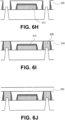
Die
6A-6L veranschaulichen Querschnittsansichten, die verschiedene Vorgänge in einem anderen Verfahren zum Herstellen einer Polycid-Schmelzbrückenstruktur für eine nicht ebene Halbleitervorrichtungsarchitektur in Übereinstimmung mit einer Ausführungsform der vorliegenden Erfindung darstellen.The6A-6L illustrate cross-sectional views depicting various operations in another method of fabricating a polycide fuse bridge structure for a non-planar semiconductor device architecture in accordance with an embodiment of the present invention. -
7 veranschaulicht eine Rechenvorrichtung in Übereinstimmung mit einer Implementierung der Erfindung.7 illustrates a computing device in accordance with an implementation of the invention.
BESCHREIBUNG DER AUSFÜHRUNGSFORMENDESCRIPTION OF THE EMBODIMENTS
CMOS-kompatible Polycid-Schmelzbrückenstrukturen und Verfahren zum Herstellen von CMOS-kompatiblen Polycid-Schmelzbrückenstrukturen sind beschrieben. In der folgenden Beschreibung sind zahlreiche spezifische Details dargelegt, wie spezifische Integrations- und Materialbedingungen, um ein tiefgehendes Verständnis der Ausführungsformen der vorliegenden Erfindung bereitzustellen. Es wird für einen Fachmann auf dem Gebiet der Erfindung offensichtlich sein, dass Ausführungsformen der vorliegenden Erfindung ohne diese spezifischen Details praktiziert werden können. In anderen Fällen sind wohlbekannte Merkmale wie integrierte Schaltkreis entwurfs auslegungen nicht ausführlich beschrieben, um die Ausführungsformen der vorliegenden Erfindung nicht unnötig zu verdecken. Ferner soll verstanden werden, dass die verschiedenen in den Figuren gezeigten Ausführungsformen veranschaulichende Darstellungen sind und nicht notwendigerweise maßstabsgetreu gezeichnet sind.CMOS compatible polycide fuse bridge structures and methods of fabricating CMOS compatible polycide fuse bridge structures are described. In the following description, numerous specific details are set forth, such as specific integration and material conditions, in order to provide a thorough understanding of embodiments of the present invention. It will be apparent to one skilled in the art that embodiments of the present invention may be practiced without these specific details. In other instances, well-known features such as integrated circuit design layouts are not described in detail so as not to unnecessarily obscure embodiments of the present invention. Further, it is to be understood that the various embodiments shown in the figures are illustrative representations and are not necessarily drawn to scale.
Die Erfindung betrifft eine Halbleiterstruktur gemäß Anspruch 1; die abhängen Ansprüche beschreiben Ausführungsformen der Erfindung.The invention relates to a semiconductor structure according to claim 1; the dependent claims describe embodiments of the invention.
Eine oder mehrere hierin beschriebene Ausführungsformen betreffen Polycid-Schmelzbrückenstrukturen und Herstellungsverfahren für eine High-K-Metall-Gate-Technologie. Ausführungsformen können eines oder mehrere aus Komplementär-Metalloxid-Halbleiter- (CMOS-) Vorrichtungen, High-K-Gate-Dielektrikum- und/oder Metall-Gate-Verarbeitungsschemata, einmal programmierbaren (OTP-) Sicherungen, Polysilizid- (Polycid-) Schmelzbrückenstrukturenund Verfahrenstechnologie und programmierbaren Sicherungen umfassen.One or more embodiments described herein relate to polycide fuse link structures and fabrication methods for high-K metal gate technology. Embodiments may include one or more of complementary metal oxide semiconductor (CMOS) devices, high-K gate dielectric and/or metal gate processing schemes, one-time programmable (OTP) fuses, polysilicide (polycide) fuse link structures and process technology, and programmable fuses.
Im Allgemeinen umfassen hierin beschriebene Zugänge Verarbeitungsintegrationsschemata, die die Herstellung eines Polycid-Sicherungselements und eine High-k-/Metall-Gate-CMOS-Technologieintegration ermöglichen. Genauer gesagt wird in einer Ausführungsform ein Lithographie- und Ätzstrukturierungsverfahren verwendet, um vor der Replacement-Gate-Verarbeitung eine Dummy-Polysilizium-Struktur zu vertiefen, um ein Polysilizium-Gate wirksam unter einem dielektrischen Zwischenschicht-Oxidfilm zu verbergen. Das konservierte Polysilizium-Gate wird dann silizidiert und als eine einmal programmierbare Sicherungsstruktur verwendet. Hierin beschriebene Ausführungsformen können eine Alternative einer Sicherungselementarchitektur für zukünftige Technologieknoten ermöglichen. Ferner stellen hierin beschriebene Ausführungsformen über Standard-Metall-Absicherungen hinausgehende Optionen bereit, die direkt in High-k- und Metall-Gate-basierte CMOS-Transistoren integriert werden können.In general, approaches described herein include processing integration schemes that enable polycide fuse element fabrication and high-k/metal gate CMOS technology integration. More specifically, in one embodiment, a lithography and etch patterning process is used to recess a dummy polysilicon structure prior to replacement gate processing to effectively hide a polysilicon gate beneath an interlayer oxide dielectric film. The preserved polysilicon gate is then silicided and used as a one-time programmable fuse structure. Embodiments described herein may enable an alternative fuse element architecture for future technology nodes. Furthermore, embodiments described herein provide options beyond standard metal fuses that can be directly integrated into high-k and metal gate based CMOS transistors.
Gate-Elektroden wurden, um einen Kontext bereitzustellen, anfänglich aus Metall (z.B. Aluminium) ausgebildet. Jedoch umfasste ein Metalloxid-Halbleiter-Feldeffekttransistor (MOSFET) für viele Technologieknoten eine Gate-Elektrode, die aus Polysilizium hergestellt war, um eine Ionenimplantierungen (z.B. um in derselben Schaltung eine Dotierung auf N- oder P-Typ kundenspezifisch zu gestalten) und Silizidierung (um einen Kontaktwiderstand zu verringern) zu gestatten. Folglich wurde auch eine dem MOSFET zugeordnete Sicherung in einer Schaltung mit silizidiertem Polysilizium hergestellt. Eine sogenannte „Gate-First“-Verfahrenssequenz wurde universell durchgeführt, um eine deckenartige Abscheidung des Polysiliziums, plasmaätzungsdefinierte Gate-Längen, leicht dotierte Spitzenregionen, dielektrische Seitenwand-Abstandsvorrichtungen und ein selbstausgerichtetes Source/Drain (d.h. zu den Gate-Elektroden) zu gestatten.To provide context, gate electrodes were initially formed from metal (e.g., aluminum). However, for many technology nodes, a metal-oxide-semiconductor field-effect transistor (MOSFET) included a gate electrode made from polysilicon to allow for ion implants (e.g., to customize doping to N- or P-type in the same circuit) and silicidation (to reduce contact resistance). Consequently, a fuse associated with the MOSFET in a circuit was also fabricated with silicidated polysilicon. A so-called "gate-first" process sequence was universally performed to allow blanket-like deposition of the polysilicon, plasma etch-defined gate lengths, lightly doped tip regions, sidewall dielectric spacers, and self-aligned source/drain (i.e., to the gate electrodes).
Da die Dimensionen der MOSFET bei neueren Technologieknoten weiter herabskaliert wurden, wurde die Polysilizium-Verarmung ein zunehmend schwerwiegendes Problem. Als Ergebnis werden Gate-Elektroden nun wieder aus Metall ausgebildet. Jedoch werden Gate-Elektroden typischerweise nicht mehr ausschließlich aus Aluminium ausgebildet. Um gewünschte Arbeitsfunktionen zu erreichen, werden die Gate-Elektroden nun üblicherweise aus einem Übergangsmetall, einer Legierung von Übergangsmetallen oder einem Übergangsmetallnitrid ausgebildet. Jedoch stellte die Übernahme des Metall-Gates auch Vorteile für ein alternatives sogenanntes „Gate-Last“-Verfahren bereit. Eine Implementierung des Gate-Last-Verfahrens umfasste ein sogenanntes „Replacement-Gate“- Verfahren, das die Verwendung unterschiedlicher Metalle für die N-FET und P-FET in der Schaltung gestattete. Als das Material in der Gate-Elektrode von Polysilizium auf Metall zurückgeändert wurde, wurden Back-End-Of-Line- (BEOL-) Metallsicherungen die StandardSicherungsstrukturen. Aufgrund einer Technologieskalierung und einer Erhöhung des Back- End-Widerstands stellt sich jedoch heraus, dass es bei Metallsicherungen schwierig ist, die Widerstandsdifferenz zwischen dem Sicherungselement und dem parasitären Führungswiderstand aufrecht zu erhalten. Andererseits befindet sich eine Polyzid-Sicherung auf derselben Ebene des Programm-Transistors und leidet typischerweise nicht unter dem Problem des niedrigen Widerstandsunterschieds, was potentiell eine verbesserte Sicherungstechnologie bereitstellt.As MOSFET dimensions continued to be scaled down at newer technology nodes, polysilicon depletion became an increasingly serious problem. As a result, gate electrodes are now again formed from metal. However, gate electrodes are no longer typically formed exclusively from aluminum. To achieve desired performance functions, gate electrodes are now typically formed from a transition metal, an alloy of transition metals, or a transition metal nitride. However, the adoption of the metal gate also provided advantages for an alternative so-called "gate-last" process. One implementation of the gate-last process involved a so-called "replacement-gate" process that allowed the use of different metals for the N-FET and P-FET in the circuit. When the material in the gate electrode was changed back from polysilicon to metal, back-end-of-line (BEOL) metal fuses became the standard fuse structures. However, due to technology scaling and increase in back-end resistance, metal fuses are found to be difficult to maintain the resistance difference between the fuse element and the parasitic lead resistor. On the other hand, a polycide fuse is located at the same level of the program transistor and typically does not suffer from the low resistance difference problem, potentially providing an improved fuse technology.
Ferner können hierin beschriebene Ausführungsformen mit Vorrichtungen und Architekturen des ebenen Typs kompatibel sein, aber sie können auch mit nicht ebenen Architekturen kompatibel sein. Daher sind in Übereinstimmung mit einer oder mehreren Ausführungsformen der vorliegenden Erfindung auch Polycid-Schmelzbrückenstruktur-Ausbildungsverfahren auf nicht ebenen High-k-/Metall-Gate-Technologien beschrieben.Furthermore, embodiments described herein may be compatible with planar type devices and architectures, but they may also be compatible with non-planar architectures. Therefore, in accordance with one or more embodiments of the present The invention also describes polycide fused bridge structure formation processes on non-planar high-k/metal gate technologies.
Wie in Verbindung mit den Figuren nachfolgend ausführlicher beschrieben betreffen eine oder mehrere Ausführungsformen Verfahrensintegrationsschemata, die während der High-k- und Metall-Gate-CMOS-Technologie-Herstellung eine Polysilizium-Konservierung in bestimmten Regionen gestatten. Das Polysilizium wird für eine spätere Herstellung eines Sicherungselements konserviert, das z.B. während eines Poly-Strukturierungsverfahrens strukturiert wird. Eine Lithographie-Verarbeitung kann durchgeführt werden, um den Polysilizium-Konservierungsbereich des Integrationsschemas zu ermöglichen. In einer solchen Ausführungsform wird eine Poly-Leitung für eine letztliche Anwendung als ein Polyzid-Sicherungselement freigelegt, während die anderen Poly-Gate-Regionen mit einem Photoresist bedeckt sind. Anschließend kann eine Trockenätzverarbeitung durchgeführt werden, während derer das Poly-Sicherungselement geätzt und vertieft wird. In einer solchen Ausführungsform wird zwischen dem Sicherungselement und den umgebenden Standard-Poly-Gate-Strukturen während des Ätz- und Vertiefungsverfahrens eine unterschiedliche Poly-Dichte erreicht. Nach dem Strukturierungsverfahren kann ein Polysilizium-Silizidierungsverfahren durchgeführt werden, um das Polyzid-Sicherungselement herzustellen. Ein Dummy-Gate- und Gate-Replacement-Verfahren kann dann verwendet werden, um in den Standard-Gate-Regionen High-K- und Metall-Gate-basierte Transistoren herzustellen. Dann, nach einem Metall-Gate-Füll- und Polierverfahren kann eine Kontaktbildung durchgeführt werden, um eine Kontaktflächenbildung auf dem Polyzid- Sicherungselement bereitzustellen. Die oben beschriebenen Verfahren können in die CMOS- Technologie integriert werden, mit einem Ätzzusatz einer Poly-Gate-Vertiefung in Sicherungsregionen des Substrats.As described in more detail in connection with the figures below, one or more embodiments relate to process integration schemes that allow polysilicon preservation in certain regions during high-k and metal gate CMOS technology manufacturing. The polysilicon is preserved for later fabrication of a fuse element, which is patterned, e.g., during a poly patterning process. Lithography processing may be performed to enable the polysilicon preservation region of the integration scheme. In such an embodiment, a poly line is exposed for ultimate application as a polycide fuse element, while the other poly gate regions are covered with a photoresist. Subsequently, dry etch processing may be performed, during which the poly fuse element is etched and recessed. In such an embodiment, a differential poly density is achieved between the fuse element and the surrounding standard poly gate structures during the etch and recess process. After the patterning process, a polysilicon silicidation process may be performed to fabricate the polycide fuse element. A dummy gate and gate replacement process may then be used to fabricate high-K and metal gate based transistors in the standard gate regions. Then, after a metal gate fill and polish process, a contact formation may be performed to provide a contact pad formation on the polycide fuse element. The processes described above may be integrated into CMOS technology, with an etch addition of a poly gate recess in fuse regions of the substrate.
Als ein Beispiel einer CMOS-kompatiblen Polycid-Schmelzbrückenstruktur veranschaulicht
Bezugnehmend auf
Bezugnehmend auf
Die
Bezugnehmend auf
Wie durchgehend beschrieben ist ein Material Stapel für eine Polyzid-Sicherungsstruktur, die parallel zu CMOS-Transistorvorrichtungen hergestellt wird, in einer Ausführungsform aus einer unteren polykristallinen Siliziumschicht und einer oberen Metallsilizidschicht, die aus der Reaktion von z.B. Kobalt (Co) oder Nickel (Ni) mit der polykristallinen Siliziumschicht ausgebildet ist, zusammengesetzt. In einer Ausführungsform ist der Materialstapel für eine Polycid-Schmelzbrückenstruktur nicht geschmolzen und wird es nie werden, wodurch eine polykristalline Siliziumschicht und eine obere Metallsilizidschicht Zurückbleiben. In einer anderen Ausführungsform wird der Materialstapel für eine Polyzid-Sicherungsstruktur letztlich geschmolzen (z.B. durch einen Strom, der durch das Anlegen einer Spannung auf die Struktur entsteht), wodurch ein Gemisch aus Silizium und Metall verbleibt. Das bedeutet, dass die geschmolzene Sicherung keine unterscheidbare polykristalline Siliziumschicht und obere Metallsilizidschicht aufweisen kann. In einer Ausführungsform weist das polykristalline Silizium eine Korngröße von ungefähr 20 Nanometern auf.As described throughout, a material stack for a polycide fuse structure fabricated in parallel with CMOS transistor devices is, in one embodiment, composed of a bottom polycrystalline silicon layer and a top metal silicide layer formed from the reaction of, e.g., cobalt (Co) or nickel (Ni) with the polycrystalline silicon layer. In one embodiment, the material stack for a polycide fuse bridge structure is not and never will be melted, leaving a polycrystalline silicon layer and a top metal silicide layer. In another embodiment, the material stack for a polycide fuse structure is ultimately melted (e.g., by a current created by applying a voltage to the structure), leaving a mixture of silicon and metal. This means that the melted fuse may not have a distinguishable polycrystalline silicon layer and top metal silicide layer. In one embodiment, the polycrystalline silicon has a grain size of approximately 20 nanometers.
Wie durchgehend beschrieben ist eine Gate-Dielektrikum-Schicht für die CMOS-Transistorvorrichtungen, die parallel zu einer Polycid-Schmelzbrückenstruktur hergestellt wird, in einer Ausführungsform aus einem Material wie, jedoch nicht darauf beschränkt, Hafniumoxid, Hafniumoxinitrid, Hafniumsilikat, Lanthanoxid, Zirkoniumoxid, Zirkoniumsilikat, Tantaloxid, Bariumstrontiumtitanat, Bariumtitanat, Strontiumtitanat, Yttriumoxid, Aluminiumoxid, Bleiscandiumtantaloxid, Bleizinkniobat oder einer Kombination davon zusammengesetzt. Ferner kann ein Abschnitt der Gate-Dielektrikum-Schicht eine Schicht eines nativen Oxids umfassen, das aus den oberen wenigen Schichten des Substrats ausgebildet ist. In einer Ausführungsform ist die Gate-Dielektrikum-Schicht aus einem oberen High-k-Abschnitt und einem unteren Abschnitt, der aus einem Oxid eines Halbleitermaterials zusammengesetzt ist, zusammengesetzt. In einer Ausführungsform ist die Gate-Dielektrikum-Schicht aus einem oberen Abschnitt aus Hafniumoxid und einem unteren Abschnitt aus Siliziumdioxid oder Siliziumoxinitrid zusammengesetzt.As described throughout, a gate dielectric layer for the CMOS transistor devices fabricated in parallel with a polycide fuse bridge structure is, in one embodiment, composed of a material such as, but not limited to, hafnium oxide, hafnium oxynitride, hafnium silicate, lanthanum oxide, zirconium oxide, zirconium silicate, tantalum oxide, barium strontium titanate, barium titanate, strontium titanate, yttrium oxide, alumina, lead scandium tantalum oxide, lead zinc niobate, or a combination thereof. Further, a portion of the gate dielectric layer may include a layer of a native oxide formed from the top few layers of the substrate. In one embodiment, the gate dielectric layer is composed of an upper high-k portion and a lower portion composed of an oxide of a semiconductor material. In one embodiment, the gate dielectric layer is composed of an upper portion of hafnium oxide and a lower portion of silicon dioxide or silicon oxynitride.
Wie durchgehend beschrieben ist eine Gate-Dielektrikum-Schicht für die CMOS-Transistorvorrichtungen, die parallel zu einer Polycid-Schmelzbrückenstruktur hergestellt wird, in einer Ausführungsform aus einer Metallschicht wie, jedoch nicht darauf beschränkt, Metallnitriden, Metallcarbiden, Metallsiliziden, Metallaluminiden, Hafnium, Zirkonium, Titan, Tantal, Aluminium, Ruthenium, Palladium, Platin, Kobalt, Nickel oder leitenden Metalloxiden zusammengesetzt. In einer spezifischen Ausführungsform ist die Gate-Elektrode aus einem Nicht-Arbeitsfunktionseinstellungs-Füllmaterial, das oberhalb einer Metall-Arbeitsfunktionseinstellungsschicht ausgebildet ist, zusammengesetzt.As described throughout, a gate dielectric layer for the CMOS transistor devices, fabricated in parallel with a polycide fuse bridge structure, in one embodiment is composed of a metal layer such as, but not limited to, metal nitrides, metal carbides, metal silicides, metal aluminides, hafnium, zirconium, titanium, tantalum, aluminum, ruthenium, palladium, platinum, cobalt, nickel, or conductive metal oxides. In a specific embodiment, the gate electrode is composed of a non-work function setting fill material formed above a metal work function setting layer.
In einem anderen Aspekt kann eine nicht ebene Polycid-Schmelzbrückenstruktur als eine eingebettete Polycid-Schmelzbrückenstruktur mit einer nicht ebenen Architektur umfasst sein. In einer Ausführungsform wird hierin ein Verweis auf eine nicht ebene Polyzid-Sicherungsstruktur verwendet, um eine Polycid-Schmelzbrückenstruktur zu beschreiben, die eine Polysilizium-/Silizidschicht aufweist, die über einer oder mehreren Rippen, die aus einem Substrat hervorstehen, ausgebildet ist. Als ein Beispiel veranschaulicht
Auf beide Ansichten von
In einer Ausführungsform sind die erste und die zweite Vielzahl von Rippen 310 und 311 aus einem Bulk-Substrat 302 ausgebildet, wie in
Alternativ dazu umfasst das Substrat 302 eine obere epitaxiale Schicht und einen unteren Bulk-Abschnitt, wovon beide aus einem einzelnen Kristall eines Materials zusammengesetzt sein können, das Silizium, Germanium, Siliziumgermanium oder eine III-V-zusammengesetztes Halbleitermaterial umfassen kann, aber nicht darauf beschränkt ist. Eine eingreifende Isolatorschicht, die Siliziumdioxid, Siliziumnitrid oder Siliziumoxinitrid umfassen kann, aber nicht darauf beschränkt ist, kann zwischen der ober epitaxialen Schicht und dem unteren Bulk-Abschnitt angeordnet sein.Alternatively, the
Die Isolationsschicht 303 kann aus einem Material zusammengesetzt sein, das geeignet ist, um letztlich eine dauerhafte Gate-Struktur von einem darunterliegenden Bulk- Substrat elektrisch zu isolieren oder zu deren Isolierung beizutragen. Beispielsweise ist die dielektrische Isolationsschicht 303 in einer Ausführungsform aus einem dielektrischen Material wie, jedoch nicht darauf beschränkt, Siliziumdioxid, Siliziumoxinitrid, Siliziumnitrid oder Kohlenstoff-dotiertem Siliziumnitrid zusammengesetzt. Es soll verstanden werden, dass eine globale Schicht ausgebildet und dann vertieft sein kann, um letztlich die aktiven Abschnitte der Vielzahlen von Rippen 310 und 311 ffeizulegen.The
In einer Ausführungsform ist die nicht ebene Vorrichtung 304 eine nicht ebene Vorrichtung wie, jedoch nicht darauf beschränkt, eine Rippen-FET- oder Tri-Gate-Vorrichtung. In einer solchen Ausführungsform ist eine halbleitende Kanalregion der nicht ebenen Vorrichtung 304 aus einem dreidimensionalen Körper zusammengesetzt oder darin ausgebildet. In einer solchen Ausführungsform umgibt der Gate-Stapel 308 zumindest eine obere Oberfläche und ein Paar von Seitenwänden des dreidimensionalen Körpers, wie in
Wie oben erwähnt umfassen die Halbleitervorrichtungen 304 in einer Ausführungsform einen Gate-Stapel 308, der zumindest teilweise einen Abschnitt der nicht ebenen Vorrichtung 304 umgibt. In einer solchen Ausführungsform umfasst der Gate-Stapel 308 eine Gate-Dielektrikum-Schicht und eine Gate-Elektroden-Schicht (nicht einzeln gezeigt). In einer Ausführungsform ist die Gate-Elektrode des Gate-Stapels 308 aus einem Metall-Gate zusammengesetzt und die Gate-Dielektrikum-Schicht ist aus einem High-K- Material zusammengesetzt.As mentioned above, in one embodiment, the
In einer Ausführungsform sind die Abstandsvorrichtungen 314 aus einem isolierenden dielektrischen Material zusammengesetzt, wie, jedoch nicht darauf beschränkt, Siliziumdioxid, Siliziumoxinitrid oder Siliziumnitrid. In einer Ausführungsform sind Kontakte 316 aus einer Metallart hergestellt. Die Metallart kann ein reines Metall sein wie Wolfram, Nickel oder Kobalt, oder sie kann eine Legierung sein wie eine Metall-MetallLegierung oder eine Metall-Halbleiter-Legierung (z.B. wie ein Silizidmaterial).In one embodiment,
In einem anderen Aspekt kann eine ebene Polycid-Schmelzbrückenstruktur in einer nicht ebenen Architektur umfasst sein. In einer Ausführungsform wird hierin ein Verweis auf eine ebene Polycid-Schmelzbrückenstruktur verwendet, um eine Polycid-Schmelzbrückenstruktur zu beschreiben, die eine Polysilizium-/Silizid-Schicht aufweist, die angrenzend an, jedoch nicht über, einer oder mehreren Rippen ausgebildet ist, die aus einem Substrat hervorstehen. Als ein Beispiel veranschaulicht
Bezugnehmend auf
In einem ersten nicht ebenen Fier Stellungszugang veranschaulichen die
In einem zweiten nicht ebenen Herstellungsansatz veranschaulichen
In einem dritten nicht ebenen Herstellungsansatz veranschaulichen
Der obige Ansatz kann als ein vertiefter Polysilizium-Polyzid-Sicherungsansatz bezeichnet werden.The above approach can be called a recessed polysilicon-polycide fuse approach.
Daher behandeln eine oder mehrere Ausführungsformen der vorliegenden Erfindung geeignete Eigenschaften einer Polycid-Schmelzbrückenstruktur. Beispielsweise ist eine hierin beschriebene Polycid-Schmelzbrückenstruktur in einer Ausführungsform mit derzeitigen und zukünftigen Verfahrenstechnologien kompatibel, z.B. sind die ausgeführten Polyzid-Sicherungsstruktur-Strukturen mit einem Trigate- und/oder High-k-/Metall-Gate-Verfahrensfluss kompatibel, bei dem das Polysilizium von aktiven Vorrichtungen opfernd ist und mit einer Metall-Gate-Architektur auf einem nicht ebenen Trigate-Verfahren ersetzt wird.Therefore, one or more embodiments of the present invention address suitable properties of a polycide fuse bridge structure. For example, in one embodiment, a polycide fuse bridge structure described herein is compatible with current and future process technologies, e.g., the implemented polycide fuse bridge structures are compatible with a trigate and/or high-k/metal gate process flow in which the polysilicon of active devices is sacrificial and replaced with a metal gate architecture on a non-planar trigate process.
In den oben beschriebenen Ansätzen kann eine freigelegte Vielzahl von Dummy-Gates letztlich in einem Replacement-Gate-Verfahrensschema ersetzt werden. In solch einem Schema kann Dummy-Gate-Material wie Polysilizium entfernt werden und durch Material einer dauerhaften Gate-Elektrode ersetzt werden. In einer solchen Ausführungsform wird in diesem Verfahren auch eine dauerhafte Gate-Dielektrikum-Schicht ausgebildet, anstatt aus einer früheren Verarbeitung mitgenommen zu werden. In einer Ausführungsform werden, wie oben beschrieben, Strukturen, die für Polyzid-Sicherungen konserviert sind, von der Entfernung des Polysiliziums, das für eine Silizidausbildung konserviert wird, blockiert.In the approaches described above, an exposed plurality of dummy gates may ultimately be replaced in a replacement gate process scheme. In such a scheme, dummy gate material such as polysilicon may be removed and replaced with permanent gate electrode material. In such an embodiment, a permanent gate dielectric layer is also formed in this process rather than being carried over from prior processing. In one embodiment, as described above, structures preserved for polycide fuses are blocked from the removal of the polysilicon preserved for silicide formation.
In einer Ausführungsform wird die Vielzahl von Dummy-Gates durch ein Trockenätz- oder Nassätzverfahren entfernt. In einer Ausführungsform ist die Vielzahl von Dummy-Gates aus polykristallinem Silizium oder amorphem Silizium zusammengesetzt und wird durch ein Trockenätzverfahren, das SFö umfasst, entfernt. In einer anderen Ausführungsform ist die Vielzahl von Dummy-Gates aus polykristallinem Silizium oder amorphem Silizium zusammengesetzt und wird durch ein Nassätzverfahren, das wässriges NH4OH oder Tetramethylammoniumhydroxid umfasst, entfernt. In einer Ausführungsform ist die Vielzahl von Dummy-Gates aus Siliziumnitrid zusammengesetzt und wird durch ein Nassätzverfahren, das wässrige Phosphorsäure umfasst, entfernt.In one embodiment, the plurality of dummy gates are removed by a dry etching or wet etching process. In one embodiment, the plurality of dummy gates are composed of polycrystalline silicon or amorphous silicon and are removed by a dry etching process comprising SF6. In another embodiment, the plurality of dummy gates are composed of polycrystalline silicon or amorphous silicon and are removed by a wet etching process comprising aqueous NH4OH or tetramethylammonium hydroxide. In one embodiment, the plurality of dummy gates are composed of silicon nitride and are removed by a wet etching process comprising aqueous phosphoric acid.
Vielleicht allgemeiner gesagt können eine oder mehrere Ausführungsformen der vorliegenden Erfindung auch ein Gate-ausgerichtetes Kontaktverfahren betreffen. Solch ein Verfahren kann implementiert werden, um Kontaktstrukturen für eine Halbleiterstrukturherstellung auszubilden, z.B. für eine Herstellung von integrierten Schaltkreisen. In einer Ausführungsform wird ein Kontaktmuster ausgebildet und wie nach einem bestehenden Gate-Muster ausgerichtet. Im Gegensatz dazu beinhalten konventionelle Ansätze typischerweise ein zusätzliches Lithographieverfahren mit einer engen Registrierung eines lithographischen Kontaktmusters an ein bestehendes Gate-Muster in Kombination mit selektiven Kontaktätzungen. Beispielsweise kann ein konventionelles Verfahren das Strukturieren eines Poly-(Gate-)Netzes mit getrenntem Strukturieren von Kontakten und Kontaktanschlüssen umfassen.Perhaps more generally, one or more embodiments of the present invention may also relate to a gate-aligned contact process. Such a process may be implemented to form contact structures for semiconductor structure fabrication, e.g., for integrated circuit fabrication. In one embodiment, a contact pattern is formed and aligned as per an existing gate pattern. In contrast, conventional approaches typically involve an additional lithography process with close registration of a lithographic contact pattern to an existing gate pattern in combination with selective contact etches. For example, a conventional process may include patterning a poly (gate) network with separate patterning of contacts and contact pads.
F igur 7 veranschaulicht eine Rechenvorrichtung 700 in Übereinstimmung mit einer Implementierung der Erfindung. Die Rechenvorrichtung 700 nimmt eine Platine 702 auf. Die Platine 702 kann eine Anzahl von Komponenten umfassen, einschließlich, jedoch ohne sich darauf zu beschränken, eines Prozessors 704 und zumindest eines Kommunikationschips 706. Der Prozessor 704 ist physikalisch und elektrisch an die Platine 702 gekoppelt. In manchen Implementierungen ist der zumindest eine Kommunikationschip 706 auch physikalisch und elektrisch an die Platine 702 gekoppelt. In weiteren Implementierungen ist der Kommunikationschip 706 Teil des Prozessors 704.Figure 7 illustrates a
Abhängig von ihren Anwendungen kann die Rechenvorrichtung 700 andere Komponenten umfassen, die physikalisch und elektrisch an die Platine 702 gekoppelt sein können oder dies nicht sein können. Diese anderen Komponenten umfassen, sind aber nicht darauf beschränkt, einen flüchtigen Speicher (z.B. DRAM), einen nichtflüchtigen Speicher (z.B. ROM), einen Flash-Speicher, einen Grafikprozessor, einen Digitalsignalprozessor, einen Crypto-Prozessor, einen Chipsatz, eine Antenne, eine Anzeige, eine Berührungsbildschirm-Anzeige, eine Berührungsbildschirm-Steuerung, eine Batterie, einen Audio-Codec, einen Video-Codec, einen Leistungsverstärker, eine globales-Positionsbestimmungssystem- (GPS-) Vorrichtung, einen Kompass, einen Beschleunigungsmesser, ein Gyroskop, einen Lautsprecher, eine Kamera und eine Massenspeichervorrichtung (wie ein Festplattenlaufwerk, eine Compact Disk (CD), eine Digital Versatile Disk (DVD) und so weiter).Depending on its applications, the
Der Kommunikationschip 706 ermöglicht eine drahtlose Kommunikation für die Übertragung von Daten zu und von der Rechenvorrichtung 700. Der Begriff „drahtlos“ und seine Ableitungen können verwendet werden, um Schaltkreise, Vorrichtungen, Systeme, Verfahren, Techniken, Kommunikationskanäle usw. zu bezeichnen, die Daten durch die Verwendung von modulierter elektromagnetischer Strahlung durch ein nicht festes Medium kommunizieren können. Der Begriff impliziert nicht, dass die zugeordneten Vorrichtungen keine Drähte enthalten, obwohl sie dies in manchen Ausführungsform nicht tun können. Der Kommunikationschip 706 kann ein beliebiges einer Anzahl von drahtlosen Standards oder Protokollen implementieren, umfassend aber nicht beschränkt auf Wi-Fi (IEEE-802.11-Familie), WiMAX (IEEE-802.16-Familie), IEEE 802.20, Long-Term Evolution (LTE), Ev-DO, HSPA+, HSDPA+, HSUPA+, EDGE, GSM, GPRS, CDMA, TDMA, DECT, Bluetooth, Ableitungen davon sowie beliebige andere drahtlose Protokolle, die als 3G, 4G, 5G und darüber bezeichnet sind. Die Rechenvorrichtung 700 kann eine Vielzahl von Kommunikationschips 706 umfassen. Beispielsweise kann ein erster Kommunikationschip 706 drahtlosen Kommunikationswegen kürzerer Reichweite wie Wi-Fi und Bluetooth gewidmet sein, und ein zweiter Kommunikationschip 706 kann drahtlosen Kommunikationswegen größerer Reichweite wie GPS, EDGE, GPRS, CDMA, WiMAX, LTE, Ev-DO und anderen gewidmet sein.The
Der Prozessor 704 der Rechenvorrichtung 700 umfasst einen integrierten Schaltkreis-Nacktchip, der innerhalb des Prozessors 704 eingepackt ist. In manchen Ausführungsformen der Erfindung umfasst der integrierte Schaltkreis-Nacktchip des Prozessors eine oder mehrere passive Vorrichtungen, wie Polycid-Schmelzbrückenstrukturen, die in Übereinstimmung mit Implementierungen der Erfindung gebaut sind. Der Begriff „Prozessor“ kann sich auf eine beliebige Vorrichtung oder einen beliebigen Teil einer Vorrichtung beziehen, die/der elektronische Daten aus Registern und/oder einem Speicher verarbeitet, um diese elektronischen Daten in andere elektronische Daten umzuwandeln, die in Registern und/oder einem Speicher gespeichert werden können.The
Der Kommunikationschip 706 umfasst auch einen integrierten Schaltkreis-Nacktchip, der innerhalb des Kommunikationschips 706 eingepackt ist. In Übereinstimmung mit einer anderen Implementierung der Erfindung umfasst der integrierte Schaltkreis-Nacktchip des Kommunikationschips eine oder mehrere passive Vorrichtungen wie Polyzid-Sicherungsstrukturen, die in Übereinstimmung mit Implementierungen der Erfindung gebaut sind.The
In weiteren Implementierungen kann eine andere Komponente, die innerhalb der Rechenvorrichtung 700 aufgenommen ist, einen integrierten Schaltkreis-Nacktchip enthalten, der eine oder mehrere passive Vorrichtungen wie Polycid-Schmelzbrückenstrukturen umfasst, die in Übereinstimmung mit Implementierungen der Erfindung gebaut sind.In further implementations, another component housed within the
In verschiedenen Implementierungen kann die Rechenvorrichtung 700 ein Laptop, ein Netbook, ein Notebook, ein Ultrabook, ein Smartphone, ein Tablet-PC, ein persönlicher digitaler Assistent (PDA), ein ultra-mobiler PC, ein Mobiltelefon, ein Desktop-Computer, ein Server, ein Drucker, ein Scanner, ein Monitor, eine Set-Top-Box, eine Unterhaltungssteuerungseinheit, eine Digitalkamera, ein tragbares Musikabspielgerät oder ein digitales Videoaufnahmegerät sein. In weiteren Implementierungen kann die Rechenvorrichtung 700 eine beliebige andere elektronische Vorrichtung sein, die Daten verarbeitet.In various implementations,
Daher umfassen Ausführungsformen der vorliegenden Erfindung CMOS-kompatible Polycid-Schmelzbrückenstrukturen.Therefore, embodiments of the present invention include CMOS compatible polycide fuse bridge structures.
In einer Ausführungsform umfasst eine Halbleiterstruktur ein Substrat. Eine Polyzid-Sicherungsstruktur ist oberhalb des Substrats angeordnet und umfasst Silizium und ein Metall. Eine Metalloxid-Halbleiter- (MOS-) Transistorstruktur ist oberhalb des Substrats angeordnet und umfasst eine Metall-Gate-Elektrode.In one embodiment, a semiconductor structure includes a substrate. A polycide fuse structure is disposed above the substrate and includes silicon and a metal. A metal oxide semiconductor (MOS) transistor structure is disposed above the substrate and includes a metal gate electrode.
In einer Ausführungsform ist die Polycid-Schmelzbrückenstruktur nicht programmiert und ist aus einer Schicht aus Metallsilizid auf einer Schicht aus Polysilizium zusammengesetzt.In one embodiment, the polycide fuse bridge structure is unprogrammed and is composed of a layer of metal silicide on a layer of polysilicon.
In einer Ausführungsform ist die Polycid-Schmelzbrückenstruktur programmiert und ist aus einem Gemisch des Siliziums und des Metalls zusammengesetzt.In one embodiment, the polycide fuse bridge structure is programmed and is composed of a mixture of the silicon and the metal.
Die MOS-Transistorstruktur umfasst ferner eine High-k- Gate-Dielektrikum-Schicht.The MOS transistor structure further includes a high-k gate dielectric layer.
In einer Ausführungsform ist die High-k-Gate-Dielektrikum-Schicht zwischen der Metall-Gate-Elektrode und dem Substrat sowie entlang von Seitenwänden der Metall-Gate-Elektrode angeordnet.In one embodiment, the high-k gate dielectric layer is disposed between the metal gate electrode and the substrate and along sidewalls of the metal gate electrode.
In einer Ausführungsform ist das Metall der Polycid-Schmelzbrückenstruktur Nickel oder Kobalt.In one embodiment, the metal of the polycide fusion bridge structure is nickel or cobalt.
In einer Ausführungsform ist das Substrat ein einkristallines Bulk-Silizium-Substrat, die MOS-Transistorstruktur ist auf dem einkristallinen Bulk-Silizium-Substrat angeordnet und die Polycid-Schmelzbrückenstruktur ist auf einer Isolationsregion angeordnet, die in dem einkristallinen Bulk-Silizium-Substrat angeordnet ist.In one embodiment, the substrate is a bulk single crystal silicon substrate, the MOS transistor structure is disposed on the bulk single crystal silicon substrate, and the polycide fuse bridge structure is disposed on an isolation region disposed in the bulk single crystal silicon substrate.
In einer Ausführungsform umfasst eine Halbleiterstruktur erste und zweite Halbleiterrippen, die oberhalb eines Substrats angeordnet sind. Eine Polyzid-Sicherungsstruktur ist oberhalb der ersten Halbleiterrippe angeordnet, aber nicht oberhalb der zweiten Halbleiterrippe. Die Polycid-Schmelzbrückenstruktur umfasst Silizium und ein Metall.In one embodiment, a semiconductor structure comprises first and second semiconductor fins disposed above a substrate. A polycide fuse structure is disposed above the first semiconductor fin, but not above the second semiconductor fin. The polycide fuse structure comprises silicon and a metal.
Eine Metalloxid-Halbleiter- (MOS-) Transistorstruktur ist aus der zweiten Halbleiterrippe ausgebildet, aber nicht aus der ersten Halbleiterrippe. Die MOS-Transistorstruktur umfasst eine Metall-Gate-Elektrode.A metal oxide semiconductor (MOS) transistor structure is formed from the second semiconductor fin but not from the first semiconductor fin. The MOS transistor structure includes a metal gate electrode.
In einer Ausführungsform ist die Polycid-Schmelzbrückenstruktur nicht programmiert und ist aus einer Schicht aus Metallsilizid auf einer Schicht aus Polysilizium zusammengesetzt.In one embodiment, the polycide fuse bridge structure is unprogrammed and is composed of a layer of metal silicide on a layer of polysilicon.
In einer Ausführungsform ist die Polycid-Schmelzbrückenstruktur programmiert und ist aus einem Gemisch des Siliziums und des Metalls zusammengesetzt.In one embodiment, the polycide fuse bridge structure is programmed and is composed of a mixture of the silicon and the metal.
In einer Ausführungsform umfasst die MOS-Transistorstruktur ferner eine High-k-Gate-Dielektrikum-Schicht.In one embodiment, the MOS transistor structure further comprises a high-k gate dielectric layer.
In einer Ausführungsform ist die High-k-Gate-Dielektrikum-Schicht zwischen der Metall-Gate-Elektrode und der zweiten Halbleiterrippe sowie entlang von Seitenwänden der Metall-Gate-Elektrode angeordnet.In one embodiment, the high-k gate dielectric layer is disposed between the metal gate electrode and the second semiconductor fin and along sidewalls of the metal gate electrode.
In einer Ausführungsform ist das Metall der Polycid-Schmelzbrückenstruktur Nickel oder Kobalt.In one embodiment, the metal of the polycide fusion bridge structure is nickel or cobalt.
In einer Ausführungsform ist die Polycid-Schmelzbrückenstruktur auf einer elektrisch isolierenden Schicht angeordnet, die auf der ersten Halbleiterrippe angeordnet ist.In one embodiment, the polycide fuse bridge structure is arranged on an electrically insulating layer arranged on the first semiconductor fin.
In einer Ausführungsform entstammt die erste Halbleiterrippe einer ersten Vielzahl von Halbleiterrippen, und die zweite Halbleiterrippe entstammt einer zweiten Vielzahl von Halbleiterrippen. Die Polycid-Schmelzbrückenstruktur ist oberhalb der ersten Vielzahl von Halbleiterrippen angeordnet, aber nicht oberhalb der zweiten Vielzahl von Halbleiterrippen. Die MOS-Transistorstruktur ist aus der zweiten Vielzahl von Halbleiterrippen ausgebildet, aber nicht aus der ersten Vielzahl von Halbleiterrippen.In one embodiment, the first semiconductor fin is from a first plurality of semiconductor fins and the second semiconductor fin is from a second plurality of semiconductor fins. The polycide fuse bridge structure is arranged above the first plurality of semiconductor fins but not above the second plurality of semiconductor fins. The MOS transistor structure is formed from the second plurality of semiconductor fins but not from the first plurality of semiconductor fins.
In einer Ausführungsform sind die erste und die zweite Vielzahl von Halbleiterrippen elektrisch an ein darunterliegendes Halbleitersubstrat gekoppelt.In one embodiment, the first and second plurality of semiconductor fins are electrically coupled to an underlying semiconductor substrate.
In einer Ausführungsform ist die Polycid-Schmelzbrückenstruktur eine nicht ebene Polyzid- Sicherungsstruktur.In one embodiment, the polycide fuse bridge structure is a non-planar polycide fuse structure.
In einer Ausführungsform umfasst eine Halbleiterstruktur erste und zweite Halbleiterrippen, die oberhalb eines Substrats angeordnet sind. Eine Isolationsregion ist oberhalb des Halbleitersubstrats, zwischen den ersten und den zweiten Halbleiterrippen und in einer Höhe, die geringer als die ersten und die zweiten Halbleiterrippen ist, angeordnet. Eine Polycid-Schmelzbrückenstruktur ist oberhalb der Isolationsregion angeordnet, aber nicht oberhalb der ersten und der zweiten Halbleiterrippen. Die Polycid-Schmelzbrückenstruktur umfasst Silizium und ein Metall. Erste und zweite Metalloxid-Halbleiter- (MOS-) Transistorstrukturen sind aus den ersten bzw. den zweiten Halbleiterrippen ausgebildet. Die MOS-Transistorstrukturen umfassen jeweils eine Metall-Gate-Elektrode.In one embodiment, a semiconductor structure includes first and second semiconductor fins disposed above a substrate. An isolation region is disposed above the semiconductor substrate, between the first and second semiconductor fins, and at a height less than the first and second semiconductor fins. A polycide fuse link structure is disposed above the isolation region, but not above the first and second semiconductor fins. The polycide fuse link structure includes silicon and a metal. First and second metal oxide semiconductor (MOS) transistor structures are formed from the first and second semiconductor fins, respectively. The MOS transistor structures each include a metal gate electrode.
In einer Ausführungsform ist die Polycid-Schmelzbrückenstruktur nicht programmiert und ist aus einer Schicht aus Metallsilizid auf einer Schicht aus Polysilizium zusammengesetzt.In one embodiment, the polycide fuse bridge structure is unprogrammed and is composed of a layer of metal silicide on a layer of polysilicon.
In einer Ausführungsform ist die Polycid-Schmelzbrückenstruktur programmiert und ist aus einem Gemisch des Siliziums und des Metalls zusammengesetzt.In one embodiment, the polycide fuse bridge structure is programmed and is composed of a mixture of the silicon and the metal.
In einer Ausführungsform umfasst jede der ersten und der zweiten der MOS-Transistorstrukturen ferner eine High-k-Gate-Dielektrikum-Schicht, und die High-k-Gate-Dielektrikum-Schicht ist zwischen der Metall-Gate-Elektrode und der entsprechenden ersten oder zweiten Halbleiterrippe sowie entlang von Seitenwänden der Metall-Gate-Elektrode angeordnet.In one embodiment, each of the first and second MOS transistor structures further comprises a high-k gate dielectric layer, and the high-k gate dielectric layer is disposed between the metal gate electrode and the corresponding first or second semiconductor fin and along sidewalls of the metal gate electrode.
In einer Ausführungsform ist das Metall der Polycid-Schmelzbrückenstruktur Nickel oder Kobalt.In one embodiment, the metal of the polycide fusion bridge structure is nickel or cobalt.
In einer Ausführungsform entstammt die erste Halbleiterrippe einer ersten Vielzahl von Halbleiterrippen und die zweite Halbleiterrippe entstammt einer zweiten Vielzahl von Halbleiterrippen. Die erste MOS-Transistorstruktur ist aus der ersten Vielzahl von Halbleiterrippen ausgebildet und die zweite MOS-Transistorstruktur ist aus der zweiten Vielzahl von Halbleiterrippen ausgebildet. Die erste und die zweite Vielzahl von Halbleiterrippen sind elektrisch an ein darunterliegendes Bulk-Halbleitersubstrat gekoppelt.In one embodiment, the first semiconductor fin is from a first plurality of semiconductor fins and the second semiconductor fin is from a second plurality of semiconductor fins. The first MOS transistor structure is formed from the first plurality of semiconductor fins and the second MOS transistor structure is formed from the second plurality of semiconductor fins. The first and the second plurality of semiconductor fins are electrically coupled to an underlying bulk semiconductor substrate.
In einer Ausführungsform ist die Polycid-Schmelzbrückenstruktur eine ebene Polyzid-Sicherungsstruktur.In one embodiment, the polycide fuse bridge structure is a planar polycide fuse structure.
In einer Ausführungsform weist die Polycid-Schmelzbrückenstruktur in einer Höhe, die geringer als die Höhen der ersten und der zweiten Halbleiterrippen ist, eine oberste Oberfläche auf.In one embodiment, the polycide fuse bridge structure has a top surface at a height less than the heights of the first and second semiconductor fins.
Claims (20)
Applications Claiming Priority (1)
| Application Number | Priority Date | Filing Date | Title |
|---|---|---|---|
| PCT/US2013/047626 WO2014209285A1 (en) | 2013-06-25 | 2013-06-25 | Cmos-compatible polycide fuse structure and method of fabricating same |
Publications (2)
| Publication Number | Publication Date |
|---|---|
| DE112013007051T5 DE112013007051T5 (en) | 2016-03-03 |
| DE112013007051B4 true DE112013007051B4 (en) | 2025-02-13 |
Family
ID=52142429
Family Applications (1)
| Application Number | Title | Priority Date | Filing Date |
|---|---|---|---|
| DE112013007051.0T Expired - Fee Related DE112013007051B4 (en) | 2013-06-25 | 2013-06-25 | CMOS-compatible polycide fuse bridge structure |
Country Status (7)
| Country | Link |
|---|---|
| US (1) | US9881927B2 (en) |
| KR (2) | KR102241180B1 (en) |
| CN (1) | CN105283961B (en) |
| DE (1) | DE112013007051B4 (en) |
| GB (1) | GB2529955B (en) |
| TW (1) | TWI567940B (en) |
| WO (1) | WO2014209285A1 (en) |
Families Citing this family (13)
| Publication number | Priority date | Publication date | Assignee | Title |
|---|---|---|---|---|
| US8890260B2 (en) * | 2009-09-04 | 2014-11-18 | Taiwan Semiconductor Manufacturing Company, Ltd. | Polysilicon design for replacement gate technology |
| US11574867B2 (en) * | 2020-11-25 | 2023-02-07 | Globalfoundries U.S. Inc. | Non-planar silicided semiconductor electrical fuse |
| US9728642B2 (en) * | 2015-11-04 | 2017-08-08 | International Business Machines Corporation | Retaining strain in finFET devices |
| US9754875B1 (en) * | 2016-07-20 | 2017-09-05 | International Business Machines Corporation | Designable channel FinFET fuse |
| US10522536B2 (en) * | 2016-08-03 | 2019-12-31 | Taiwan Semiconductor Manufacturing Co., Ltd. | Structure and formation method of semiconductor device with gate stacks |
| US11289483B2 (en) | 2016-12-23 | 2022-03-29 | Intel Corporation | Metal fuse and self-aligned gate edge (SAGE) architecture having a metal fuse |
| KR102387465B1 (en) | 2017-03-09 | 2022-04-15 | 삼성전자주식회사 | Semiconductor devices and method of manufacturing the same |
| CN107256855B (en) * | 2017-07-11 | 2019-07-12 | 上海华力微电子有限公司 | A kind of fuse and its manufacturing method |
| US10304685B2 (en) * | 2017-08-14 | 2019-05-28 | United Microelectronics Corp. | Manufacturing method of integrated circuit |
| US10720513B2 (en) | 2018-03-09 | 2020-07-21 | Globalfoundries Singapore Pte. Ltd. | OTP-MTP on FDSOI architecture and method for producing the same |
| US11081562B2 (en) * | 2020-01-06 | 2021-08-03 | Nanya Technology Corporation | Semiconductor device with a programmable contact and method for fabricating the same |
| US12604726B2 (en) * | 2022-08-02 | 2026-04-14 | Globalfoundries Singapore Pte. Ltd. | Electronic fuse |
| US12506070B2 (en) * | 2023-01-06 | 2025-12-23 | Globalfoundries U.S. Inc. | Electronically programmable fuse with heating transistors |
Citations (2)
| Publication number | Priority date | Publication date | Assignee | Title |
|---|---|---|---|---|
| US20060208274A1 (en) | 2004-03-26 | 2006-09-21 | Chi-Hsi Wu | Electrical fuse for silicon-on-insulator devices |
| US20100133649A1 (en) | 2008-12-02 | 2010-06-03 | Yung-Chang Lin | Contact efuse structure, method of making a contact efuse device containing the same, and method of making a read only memory containing the same |
Family Cites Families (14)
| Publication number | Priority date | Publication date | Assignee | Title |
|---|---|---|---|---|
| US6208549B1 (en) * | 2000-02-24 | 2001-03-27 | Xilinx, Inc. | One-time programmable poly-fuse circuit for implementing non-volatile functions in a standard sub 0.35 micron CMOS |
| JP2002237524A (en) * | 2001-02-09 | 2002-08-23 | Seiko Instruments Inc | Complementary MOS semiconductor device |
| KR100425452B1 (en) * | 2001-07-04 | 2004-03-30 | 삼성전자주식회사 | Method of opening repair fuse of semiconductor device |
| US20070111403A1 (en) * | 2005-11-15 | 2007-05-17 | Chun Jiang | Polycide fuse with reduced programming time |
| US7960760B2 (en) | 2006-12-28 | 2011-06-14 | Texas Instruments Incorporated | Electrically programmable fuse |
| JP2009016706A (en) * | 2007-07-09 | 2009-01-22 | Sony Corp | Semiconductor device and manufacturing method thereof |
| US20090243032A1 (en) * | 2008-03-27 | 2009-10-01 | Shi-Bai Chen | Electrical fuse structure |
| US8159040B2 (en) * | 2008-05-13 | 2012-04-17 | International Business Machines Corporation | Metal gate integration structure and method including metal fuse, anti-fuse and/or resistor |
| KR20100010724A (en) * | 2008-07-23 | 2010-02-02 | 주식회사 하이닉스반도체 | Semiconductor device having fuse and fabricating method of the same |
| US8053809B2 (en) * | 2009-05-26 | 2011-11-08 | International Business Machines Corporation | Device including high-K metal gate finfet and resistive structure and method of forming thereof |
| US7927977B2 (en) | 2009-07-15 | 2011-04-19 | Sandisk 3D Llc | Method of making damascene diodes using sacrificial material |
| US8492286B2 (en) * | 2010-11-22 | 2013-07-23 | International Business Machines Corporation | Method of forming E-fuse in replacement metal gate manufacturing process |
| US8716831B2 (en) | 2011-09-29 | 2014-05-06 | Broadcom Corporation | One time programmable structure using a gate last high-K metal gate process |
| US9466696B2 (en) * | 2012-01-24 | 2016-10-11 | Taiwan Semiconductor Manufacturing Company, Ltd. | FinFETs and methods for forming the same |
-
2013
- 2013-06-25 KR KR1020207008983A patent/KR102241180B1/en not_active Expired - Fee Related
- 2013-06-25 KR KR1020157031743A patent/KR102101763B1/en not_active Expired - Fee Related
- 2013-06-25 CN CN201380076882.3A patent/CN105283961B/en active Active
- 2013-06-25 US US14/780,222 patent/US9881927B2/en not_active Expired - Fee Related
- 2013-06-25 WO PCT/US2013/047626 patent/WO2014209285A1/en not_active Ceased
- 2013-06-25 GB GB1520616.2A patent/GB2529955B/en not_active Expired - Fee Related
- 2013-06-25 DE DE112013007051.0T patent/DE112013007051B4/en not_active Expired - Fee Related
-
2014
- 2014-06-16 TW TW103120699A patent/TWI567940B/en active
Patent Citations (2)
| Publication number | Priority date | Publication date | Assignee | Title |
|---|---|---|---|---|
| US20060208274A1 (en) | 2004-03-26 | 2006-09-21 | Chi-Hsi Wu | Electrical fuse for silicon-on-insulator devices |
| US20100133649A1 (en) | 2008-12-02 | 2010-06-03 | Yung-Chang Lin | Contact efuse structure, method of making a contact efuse device containing the same, and method of making a read only memory containing the same |
Also Published As
| Publication number | Publication date |
|---|---|
| US20160056162A1 (en) | 2016-02-25 |
| CN105283961B (en) | 2019-11-05 |
| KR102101763B1 (en) | 2020-04-20 |
| KR20200036057A (en) | 2020-04-06 |
| KR20160026849A (en) | 2016-03-09 |
| TW201513304A (en) | 2015-04-01 |
| KR102241180B1 (en) | 2021-04-16 |
| US9881927B2 (en) | 2018-01-30 |
| TWI567940B (en) | 2017-01-21 |
| WO2014209285A1 (en) | 2014-12-31 |
| DE112013007051T5 (en) | 2016-03-03 |
| CN105283961A (en) | 2016-01-27 |
| GB2529955A (en) | 2016-03-09 |
| GB2529955B (en) | 2020-01-22 |
| GB201520616D0 (en) | 2016-01-06 |
Similar Documents
| Publication | Publication Date | Title |
|---|---|---|
| DE112013007051B4 (en) | CMOS-compatible polycide fuse bridge structure | |
| DE112011105996B4 (en) | Semiconductor component with a narrowed semiconductor body | |
| DE112011106052B4 (en) | Integration of dielectric multigate transistors in a tri-gate process (FINFET) | |
| DE102020103517A1 (en) | Gate-all-around structures for integrated circuits with source or drain structures with epitaxial knobs | |
| DE102020134411A1 (en) | INTEGRATED GATE-ALL-AROUND STRUCTURES WITH GERMANIUM-DOPED NANOBAND CHANNEL STRUCTURES | |
| DE102019121697A1 (en) | Integrated gate all-round circuit structures with asymmetrical source and drain contact structures | |
| DE112016007034T5 (en) | TRIGATE AND FINFET COMPONENTS WITH SELF-ALIGNED GATE EDGE | |
| DE102021121273A1 (en) | FABRICATION OF GATE ALL AROUND INTEGRATED CIRCUIT STRUCTURES WITH PRE-SPACER DEPOSITION CUT GATES | |
| DE112016007299T5 (en) | BACK SOURCE / DRAIN REPLACEMENT FOR SEMICONDUCTOR ELEMENTS WITH METALLIZATION ON BOTH SIDES | |
| DE102019132137A1 (en) | INTEGRATED GATE ALL-AROUND CIRCUIT STRUCTURES WITH OXIDE PARTIAL FINES | |
| DE112016007104T5 (en) | DUAL FINN END CAP FOR SELF-ADJUSTED (SAGE) ARCHITECTURES | |
| DE102020128908A1 (en) | Integrated gate-all-around circuit structures that have components with electrical channel-substrate contact | |
| DE102019108021A1 (en) | Wrap-around contact structures for semiconductor fins | |
| DE102020130392A1 (en) | INTEGRATED CIRCUIT STRUCTURES WITH ALL-ROUND GATE THAT HAVE DEVICES WITH AN ELECTRICAL SOURCE / DRAIN SUBSTRATE CONTACT | |
| DE102020132236A1 (en) | INTEGRATED CIRCUIT STRUCTURES WITH ALL-ROUND GATE WITH FIN STACK INSULATION | |
| DE102020128647A1 (en) | GATE-ALL-AROUND-INTEGRATED CIRCUIT STRUCTURES WITH INSULATING SUBSTRATE | |
| DE102021121941A1 (en) | LOW-RESISTANCE APPROACHES FOR MAKING CONTACTS AND THE RESULTING STRUCTURES | |
| DE102023210626A1 (en) | INTEGRATED CIRCUIT STRUCTURES WITH UNIFORM METAL GATE AND TRENCH CONTACT PLUG FOR TUB GATES WITH PYRAMID-SHAPED CHANNEL STRUCTURES | |
| DE112022002055T5 (en) | INTEGRATED CIRCUIT STRUCTURES WITH A METAL GATE PLUG SITTING ON A DIELECTRIC DUMMY FIN | |
| DE112016007366T5 (en) | SEMICONDUCTOR DEVICE HAVING FINNENDS VOLTAGE INDUCING FEATURES | |
| DE102024119428A1 (en) | Gate-all-around integrated circuit structures with depopulated channel structures using separate source or drain approaches | |
| DE112015006960T5 (en) | LANG CHANNEL MOS TRANSISTORS FOR CRAZY LOSS ARMS APPLICATIONS ON A SHORT CHANNEL CMOS CHIP | |
| DE102020131752A1 (en) | GATE END CAP ARCHITECTURES THAT HAVE A RELATIVELY SHORT VERTICAL STACK | |
| DE102023134680A1 (en) | INTEGRATED CIRCUIT STRUCTURES WITH REAR CONDUCTIVE SOURCE OR DRAIN CONTACT WITH IMPROVED CONTACT AREA | |
| DE112022006021T5 (en) | GATE-ALL-AROUND INTEGRATED CIRCUIT STRUCTURES WITH RAISED WALL STRUCTURES FOR EPITATICAL SOURCE OR DRAIN AREA LIMITATION |
Legal Events
| Date | Code | Title | Description |
|---|---|---|---|
| R012 | Request for examination validly filed | ||
| R081 | Change of applicant/patentee |
Owner name: TAHOE RESEARCH, LTD., IE Free format text: FORMER OWNER: INTEL CORP., SANTA CLARA, CALIF., US |
|
| R082 | Change of representative |
Representative=s name: VOSSIUS & PARTNER PATENTANWAELTE RECHTSANWAELT, DE |
|
| R016 | Response to examination communication | ||
| R079 | Amendment of ipc main class |
Free format text: PREVIOUS MAIN CLASS: H01L0029780000 Ipc: H01L0027118000 |
|
| R018 | Grant decision by examination section/examining division | ||
| R079 | Amendment of ipc main class |
Free format text: PREVIOUS MAIN CLASS: H01L0027118000 Ipc: H10D0084900000 |
|
| R020 | Patent grant now final | ||
| R119 | Application deemed withdrawn, or ip right lapsed, due to non-payment of renewal fee |