DE10296322B4 - Image sensor and method of making the same - Google Patents
Image sensor and method of making the same Download PDFInfo
- Publication number
- DE10296322B4 DE10296322B4 DE10296322T DE10296322T DE10296322B4 DE 10296322 B4 DE10296322 B4 DE 10296322B4 DE 10296322 T DE10296322 T DE 10296322T DE 10296322 T DE10296322 T DE 10296322T DE 10296322 B4 DE10296322 B4 DE 10296322B4
- Authority
- DE
- Germany
- Prior art keywords
- electrodes
- image sensor
- hole type
- plate
- layer
- Prior art date
- Legal status (The legal status is an assumption and is not a legal conclusion. Google has not performed a legal analysis and makes no representation as to the accuracy of the status listed.)
- Expired - Fee Related
Links
- 238000004519 manufacturing process Methods 0.000 title claims description 18
- 239000004065 semiconductor Substances 0.000 claims abstract description 39
- 229910004613 CdTe Inorganic materials 0.000 claims description 43
- 239000000758 substrate Substances 0.000 claims description 32
- 229910052738 indium Inorganic materials 0.000 claims description 20
- APFVFJFRJDLVQX-UHFFFAOYSA-N indium atom Chemical compound [In] APFVFJFRJDLVQX-UHFFFAOYSA-N 0.000 claims description 20
- 229910004611 CdZnTe Inorganic materials 0.000 claims description 12
- 239000010931 gold Substances 0.000 claims description 8
- XLYOFNOQVPJJNP-UHFFFAOYSA-N water Substances O XLYOFNOQVPJJNP-UHFFFAOYSA-N 0.000 claims description 6
- PCHJSUWPFVWCPO-UHFFFAOYSA-N gold Chemical compound [Au] PCHJSUWPFVWCPO-UHFFFAOYSA-N 0.000 claims description 5
- 229910052737 gold Inorganic materials 0.000 claims description 5
- 239000011159 matrix material Substances 0.000 claims description 5
- 229920005989 resin Polymers 0.000 claims description 5
- 239000011347 resin Substances 0.000 claims description 5
- 239000002184 metal Substances 0.000 claims description 3
- 229910052751 metal Inorganic materials 0.000 claims description 3
- 239000002131 composite material Substances 0.000 claims 1
- 238000007654 immersion Methods 0.000 claims 1
- 239000010410 layer Substances 0.000 description 67
- 238000001514 detection method Methods 0.000 description 18
- 238000000034 method Methods 0.000 description 14
- 239000000463 material Substances 0.000 description 9
- 239000011241 protective layer Substances 0.000 description 7
- 230000005855 radiation Effects 0.000 description 7
- 238000005336 cracking Methods 0.000 description 6
- 238000010586 diagram Methods 0.000 description 6
- 150000001875 compounds Chemical class 0.000 description 5
- 230000035945 sensitivity Effects 0.000 description 5
- 239000002245 particle Substances 0.000 description 4
- 241000282412 Homo Species 0.000 description 3
- 238000000605 extraction Methods 0.000 description 3
- 238000001465 metallisation Methods 0.000 description 3
- 238000012986 modification Methods 0.000 description 3
- 230000004048 modification Effects 0.000 description 3
- 239000000126 substance Substances 0.000 description 3
- 229910052793 cadmium Inorganic materials 0.000 description 2
- JJWKPURADFRFRB-UHFFFAOYSA-N carbonyl sulfide Chemical compound O=C=S JJWKPURADFRFRB-UHFFFAOYSA-N 0.000 description 2
- 238000005516 engineering process Methods 0.000 description 2
- 239000000284 extract Substances 0.000 description 2
- 239000007788 liquid Substances 0.000 description 2
- 238000007747 plating Methods 0.000 description 2
- 239000000843 powder Substances 0.000 description 2
- 238000004544 sputter deposition Methods 0.000 description 2
- 238000012360 testing method Methods 0.000 description 2
- MARUHZGHZWCEQU-UHFFFAOYSA-N 5-phenyl-2h-tetrazole Chemical compound C1=CC=CC=C1C1=NNN=N1 MARUHZGHZWCEQU-UHFFFAOYSA-N 0.000 description 1
- 239000004593 Epoxy Substances 0.000 description 1
- LFQSCWFLJHTTHZ-UHFFFAOYSA-N Ethanol Chemical compound CCO LFQSCWFLJHTTHZ-UHFFFAOYSA-N 0.000 description 1
- 229910001218 Gallium arsenide Inorganic materials 0.000 description 1
- 239000004642 Polyimide Substances 0.000 description 1
- BQCADISMDOOEFD-UHFFFAOYSA-N Silver Chemical compound [Ag] BQCADISMDOOEFD-UHFFFAOYSA-N 0.000 description 1
- 230000002411 adverse Effects 0.000 description 1
- 230000003471 anti-radiation Effects 0.000 description 1
- 229910052797 bismuth Inorganic materials 0.000 description 1
- JCXGWMGPZLAOME-UHFFFAOYSA-N bismuth atom Chemical compound [Bi] JCXGWMGPZLAOME-UHFFFAOYSA-N 0.000 description 1
- BDOSMKKIYDKNTQ-UHFFFAOYSA-N cadmium atom Chemical compound [Cd] BDOSMKKIYDKNTQ-UHFFFAOYSA-N 0.000 description 1
- CEKJAYFBQARQNG-UHFFFAOYSA-N cadmium zinc Chemical compound [Zn].[Cd] CEKJAYFBQARQNG-UHFFFAOYSA-N 0.000 description 1
- 238000006243 chemical reaction Methods 0.000 description 1
- 239000012141 concentrate Substances 0.000 description 1
- 238000005520 cutting process Methods 0.000 description 1
- 230000001419 dependent effect Effects 0.000 description 1
- 230000001627 detrimental effect Effects 0.000 description 1
- 238000011161 development Methods 0.000 description 1
- 239000003814 drug Substances 0.000 description 1
- 230000005684 electric field Effects 0.000 description 1
- 239000003822 epoxy resin Substances 0.000 description 1
- 238000002474 experimental method Methods 0.000 description 1
- 230000005251 gamma ray Effects 0.000 description 1
- 229910052732 germanium Inorganic materials 0.000 description 1
- 239000011521 glass Substances 0.000 description 1
- 238000002844 melting Methods 0.000 description 1
- 230000008018 melting Effects 0.000 description 1
- 238000002156 mixing Methods 0.000 description 1
- 238000012544 monitoring process Methods 0.000 description 1
- 238000009659 non-destructive testing Methods 0.000 description 1
- 229910052697 platinum Inorganic materials 0.000 description 1
- 229920000647 polyepoxide Polymers 0.000 description 1
- 229920001721 polyimide Polymers 0.000 description 1
- 239000002901 radioactive waste Substances 0.000 description 1
- 229910052710 silicon Inorganic materials 0.000 description 1
- 229910052709 silver Inorganic materials 0.000 description 1
- 239000004332 silver Substances 0.000 description 1
- 239000002689 soil Substances 0.000 description 1
- 229910000679 solder Inorganic materials 0.000 description 1
- 229910001220 stainless steel Inorganic materials 0.000 description 1
- 239000010935 stainless steel Substances 0.000 description 1
- 229910052714 tellurium Inorganic materials 0.000 description 1
- PORWMNRCUJJQNO-UHFFFAOYSA-N tellurium atom Chemical compound [Te] PORWMNRCUJJQNO-UHFFFAOYSA-N 0.000 description 1
- 230000008646 thermal stress Effects 0.000 description 1
- 238000012546 transfer Methods 0.000 description 1
- 238000007740 vapor deposition Methods 0.000 description 1
Images


Classifications
-
- H—ELECTRICITY
- H10—SEMICONDUCTOR DEVICES; ELECTRIC SOLID-STATE DEVICES NOT OTHERWISE PROVIDED FOR
- H10F—INORGANIC SEMICONDUCTOR DEVICES SENSITIVE TO INFRARED RADIATION, LIGHT, ELECTROMAGNETIC RADIATION OF SHORTER WAVELENGTH OR CORPUSCULAR RADIATION
- H10F39/00—Integrated devices, or assemblies of multiple devices, comprising at least one element covered by group H10F30/00, e.g. radiation detectors comprising photodiode arrays
- H10F39/10—Integrated devices
- H10F39/12—Image sensors
- H10F39/191—Photoconductor image sensors
- H10F39/195—X-ray, gamma-ray or corpuscular radiation imagers
-
- G—PHYSICS
- G01—MEASURING; TESTING
- G01T—MEASUREMENT OF NUCLEAR OR X-RADIATION
- G01T1/00—Measuring X-radiation, gamma radiation, corpuscular radiation, or cosmic radiation
- G01T1/16—Measuring radiation intensity
- G01T1/24—Measuring radiation intensity with semiconductor detectors
- G01T1/241—Electrode arrangements, e.g. continuous or parallel strips or the like
-
- H—ELECTRICITY
- H04—ELECTRIC COMMUNICATION TECHNIQUE
- H04N—PICTORIAL COMMUNICATION, e.g. TELEVISION
- H04N23/00—Cameras or camera modules comprising electronic image sensors; Control thereof
- H04N23/50—Constructional details
- H04N23/54—Mounting of pick-up tubes, electronic image sensors, deviation or focusing coils
-
- H—ELECTRICITY
- H10—SEMICONDUCTOR DEVICES; ELECTRIC SOLID-STATE DEVICES NOT OTHERWISE PROVIDED FOR
- H10F—INORGANIC SEMICONDUCTOR DEVICES SENSITIVE TO INFRARED RADIATION, LIGHT, ELECTROMAGNETIC RADIATION OF SHORTER WAVELENGTH OR CORPUSCULAR RADIATION
- H10F77/00—Constructional details of devices covered by this subclass
- H10F77/10—Semiconductor bodies
- H10F77/12—Active materials
- H10F77/123—Active materials comprising only Group II-VI materials, e.g. CdS, ZnS or HgCdTe
-
- H—ELECTRICITY
- H10—SEMICONDUCTOR DEVICES; ELECTRIC SOLID-STATE DEVICES NOT OTHERWISE PROVIDED FOR
- H10F—INORGANIC SEMICONDUCTOR DEVICES SENSITIVE TO INFRARED RADIATION, LIGHT, ELECTROMAGNETIC RADIATION OF SHORTER WAVELENGTH OR CORPUSCULAR RADIATION
- H10F39/00—Integrated devices, or assemblies of multiple devices, comprising at least one element covered by group H10F30/00, e.g. radiation detectors comprising photodiode arrays
- H10F39/011—Manufacture or treatment of image sensors covered by group H10F39/12
- H10F39/022—Manufacture or treatment of image sensors covered by group H10F39/12 of image sensors having active layers comprising only Group II-VI materials, e.g. CdS, ZnS or CdTe
-
- H—ELECTRICITY
- H10—SEMICONDUCTOR DEVICES; ELECTRIC SOLID-STATE DEVICES NOT OTHERWISE PROVIDED FOR
- H10F—INORGANIC SEMICONDUCTOR DEVICES SENSITIVE TO INFRARED RADIATION, LIGHT, ELECTROMAGNETIC RADIATION OF SHORTER WAVELENGTH OR CORPUSCULAR RADIATION
- H10F39/00—Integrated devices, or assemblies of multiple devices, comprising at least one element covered by group H10F30/00, e.g. radiation detectors comprising photodiode arrays
- H10F39/80—Constructional details of image sensors
- H10F39/809—Constructional details of image sensors of hybrid image sensors
Landscapes
- Engineering & Computer Science (AREA)
- Multimedia (AREA)
- Signal Processing (AREA)
- Physics & Mathematics (AREA)
- Health & Medical Sciences (AREA)
- Life Sciences & Earth Sciences (AREA)
- General Physics & Mathematics (AREA)
- High Energy & Nuclear Physics (AREA)
- Molecular Biology (AREA)
- Spectroscopy & Molecular Physics (AREA)
- Solid State Image Pick-Up Elements (AREA)
- Measurement Of Radiation (AREA)
- Transforming Light Signals Into Electric Signals (AREA)
- Light Receiving Elements (AREA)
Abstract
Bildsensor (10) mit: einer Platte (13), die aus einem Halbleiter hergestellt ist; einer Mehrzahl von ersten Elektroden (12) vom Lochtyp, die an der Platte (13) vorgesehen und in vorbestimmten Intervallen in einer ersten Richtung und in einer zweiten Richtung angeordnet sind; einer Mehrzahl von zweiten Elektroden (12) vom Lochtyp, die an der Platte (13) vorgesehen, in vorbestimmten Intervallen in der ersten Richtung und in der zweiten Richtung angeordnet und benachbart zu den ersten Elektroden (12) positioniert sind; einer Spannungsanlegungseinheit zum Anlegen einer ersten Spannung an die Mehrzahl von ersten Elektroden (12) vom Lochtyp und einer zweiten Spannung an die Mehrzahl von zweiten Elektroden (12) vom Lochtyp; und einer Leseeinheit zum Lesen von elektrischen Signalen von einer Mehrzahl von Sensorelementen (14), die jeweils eine erste Elektrode (12) vom Lochtyp, eine Mehrzahl von zweiten Elektroden (12) vom Lochtyp, die benachbart der ersten Elektrode (12) vom Lochtyp angeordnet...An image sensor (10) comprising: a plate (13) made of a semiconductor; a plurality of first hole type electrodes (12) provided on the plate (13) and arranged at predetermined intervals in a first direction and in a second direction; a plurality of second hole-type electrodes (12) provided on the plate (13) arranged at predetermined intervals in the first direction and the second direction and positioned adjacent to the first electrodes (12); a voltage application unit for applying a first voltage to the plurality of first hole type electrodes (12) and a second voltage to the plurality of second hole type electrodes (12); and a reading unit for reading electrical signals from a plurality of sensor elements (14) each having a first hole type electrode (12), a plurality of second hole type electrodes (12) disposed adjacent to the first hole type electrode (12) ...
Description
Technisches GebietTechnical area
Die Erfindung bezieht sich auf einen Bildsensor zur Erfassung von Strahlen und ein Verfahren zur Herstellung desselben.The invention relates to an image sensor for detecting radiation and a method for producing the same.
Hintergrund der TechnikBackground of the technique
Bildsensoren zum Erfassen von Strahlen, wie beispielsweise harten Röntgenstrahlen oder Gammastrahlen, und zum Erzeugen von Bilddaten werden auf verschiedenen Gebieten der Technologie verwendet. Der Bildsensor kann ein von einem Himmelskörper ausstrahlendes Strahlungsfeld erfassen, das analysiert werden kann, um die physikalischen Bedingungen bzw. Zustände und die räumliche Struktur des Himmelskörpers zu bestimmen. Der Bildsensor kann Röntgenstrahlen auf ein menschliches Objekt oder dergleichen anwenden und die durch dieses passierende Wellen erfassen, aus denen ein Tomogramm des menschlichen Objekts oder dergleichen erhalten werden kann. Der Bildsensor wird auf anderen Gebieten verwendet. Beispielsweise wird er in der Kerntechnik (z. B. Prüfen von in Glas eingeschlossenem radioaktiven Abfall und Strahlungsüberwachung), bei zerstörungsfreier Prüfung (z. B. Prüfung von Halbleitervorrichtungen) und bei der Ressourcen-Erhebung (z. B. Erhebung von Ressourcen im Boden) verwendet.Image sensors for detecting rays such as hard X-rays or gamma rays and for generating image data are used in various fields of technology. The image sensor can detect a radiation field emitted by a celestial body that can be analyzed to determine the physical conditions and the spatial structure of the celestial body. The image sensor can apply X-rays to a human object or the like and detect the waves passing therethrough, from which a tomogram of the human object or the like can be obtained. The image sensor is used in other fields. For example, it is used in nuclear engineering (eg testing of radioactive waste trapped in glass and radiation monitoring), non-destructive testing (eg testing of semiconductor devices) and resource surveying (eg collection of resources in soil ) used.
Der bis jetzt auf diesen Gebieten der Technik verwendete Bildsensor weist beispielsweise die nachstehend beschriebene Struktur auf.The image sensor used hitherto in these fields of the art, for example, has the structure described below.
Ein Bildsensor, der ein Si-Element oder ein Ge-Element benutzt, kann nur Röntgenstrahlen niedriger Energie einiger keV bis mehreren 10 keV umfassen. Seine Empfindlichkeit ist weit von dem Wert entfernt, der in der Praxis verlangt wird.An image sensor using a Si element or a Ge element can only include low energy x-rays of a few keV to several tens of keV. Its sensitivity is far from the value required in practice.
Sogar ein Hochempfindlichkeits-Bildsensor, der CdTe oder CdZnTe verwendet, kann elektrische Ladungen aus dem folgenden Grund nicht wirksam sammeln, solange seine Struktur eine herkömmliche bleibt. Die Halbleiterschicht kann dick ausgeführt werden, um das Streuen von Hochenergiepartikeln in dem Material zu fördern. Wenn die Schicht derart dick ist, wird der Abstand zwischen den Elektroden ansteigen. Dies senkt den Wirkungsgrad des Sammelns von elektrischen Ladungen. Folglich wird die Empfindlichkeit abnehmen. Um den Wirkungsgrad des Sammelns von elektrischen Ladungen zu verbessern, kann die Halbleiterschicht dünn ausgeführt werden. In diesem Fall wird die Streuung von Hochenergiepartikeln in dem Material unterdrückt. Die Empfindlichkeit des Bildsensors wird unvermeidlich abnehmen, obwohl der Ladungssammlungswirkungsgrad ansteigt.Even a high-sensitivity image sensor using CdTe or CdZnTe can not efficiently collect electric charges for the following reason, as long as its structure remains conventional. The semiconductor layer may be made thick to promote the scattering of high energy particles in the material. If the layer is so thick, the distance between the electrodes will increase. This lowers the efficiency of collecting electric charges. Consequently, the sensitivity will decrease. In order to improve the efficiency of collecting electric charges, the semiconductor layer can be made thin. In this case, the scattering of high energy particles in the material is suppressed. The sensitivity of the image sensor will inevitably decrease although the charge collection efficiency increases.
Aus der
Eine Aufgabe der Erfindung besteht darin, einen Bildsensor in Vorschlag zu bringen, der Strahlen, sogar diejenigen des harten Röntgenstrahlenenergiebandes, mit hoher Empfindlichkeit erfassen kann. Ferner ist es eine Aufgabe der Erfindung, ein Verfahren zur Herstellung eines derartigen Bildsensors bereitzustellen.An object of the invention is to suggest an image sensor which can detect rays, even those of the hard X-ray energy band, with high sensitivity. Further, it is an object of the invention to provide a method of manufacturing such an image sensor.
Ein weiterer Aspekt der Erfindung besteht darin, eine Lochherstellungstechnik beim Handhaben von schädlichen Substanzen, wie beispielsweise CdTe bereitzustellen, die für einen Menschen keinen nachteiligen Einfluss darstellt.Another aspect of the invention is to provide a hole-making technique in the handling of harmful substances, such as CdTe, that does not adversely affect a human.
Zur Lösung dieser Aufgabe bringt die Erfindung einen Bildsensor gemäß Anspruch 1 und ein Verfahren zur Herstellung eines Bildsensors gemäß Anspruch 13 in Vorschlag. Bevorzugte Ausführungsformen des Bildsensors und des Verfahrens sind in den abhängigen Patentansprüchen angegeben.To achieve this object, the invention provides an image sensor according to
Offenbarung der Erfindung Disclosure of the invention
Gemäß dem ersten Aspekt der Erfindung wird ein Bildsensor bereitgestellt, der umfasst: eine Platte, die aus einem Halbleiter hergestellt ist; eine Mehrzahl von ersten Elektroden vom Lochtyp, die auf der Platte vorgesehen und in vorbestimmten Intervallen in einer ersten Richtung und einer zweiten Richtung angeordnet sind; eine Mehrzahl von zweiten Elektroden vom Lochtyp, die auf der Platte vorgesehen, die in vorbestimmten Intervallen in der ersten Richtung und der zweiten Richtung angeordnet und die benachbart zu den ersten Elektroden positioniert sind; eine Spannungsanlegungseinheit, die eine erste Spannung an die Mehrzahl von ersten Elektroden vom Lochtyp und eine zweite Spannung an die Mehrzahl von zweiten Elektroden vom Lochtyp anlegt; und eine Leseeinheit zum Lesen von elektrischen Signalen von einer Mehrzahl von Sensorelementen, die jeweils eine erste Elektrode vom Lochtyp, eine Mehrzahl von zweiten Elektroden vom Lochtyp, die benachbart der ersten Elektrode vom Lochtyp positioniert sind, und den zwischen der ersten Elektrode vom Lochtyp und den zweiten Elektroden vom Lochtyp vorgesehenen Halbleiter umfassen.According to the first aspect of the invention, there is provided an image sensor comprising: a plate made of a semiconductor; a plurality of first hole-type electrodes provided on the plate and arranged at predetermined intervals in a first direction and a second direction; a plurality of second hole-type electrodes provided on the plate, which are arranged at predetermined intervals in the first direction and the second direction and which are positioned adjacent to the first electrodes; a voltage application unit applying a first voltage to the plurality of first hole type electrodes and a second voltage to the plurality of second hole type electrodes; and a reading unit for reading electrical signals from a plurality of sensor elements each including a hole type first electrode, a plurality of hole type second electrodes positioned adjacent to the first hole type electrode and the hole type first electrode comprise second hole-type electrodes.
Gemäß dem zweiten Aspekt der Erfindung wird ein Bildsensor gemäß dem ersten Aspekt bereitgestellt, bei dem die ersten und zweiten Elektroden vom Lochtyp in einer Richtung der Dicke der Platte vorgesehen sind.According to the second aspect of the invention, there is provided an image sensor according to the first aspect, wherein the first and second hole type electrodes are provided in a thickness direction of the plate.
Gemäß dem dritten Aspekt dieser Erfindung wird ein Bildsensor gemäß dem ersten Aspekt bereitgestellt, bei dem jedes Sensorelement eine erste Elektrode vom Lochtyp und eine Mehrzahl von zweiten Elektroden vom Lochtyp umfasst, die äquidistant beabstandet und äquidistant von der ersten Elektrode vom Lochtyp angeordnet sind.According to the third aspect of this invention, there is provided an image sensor according to the first aspect, wherein each sensor element comprises a first hole type electrode and a plurality of second hole type electrodes which are equidistantly spaced and equidistant from the first hole type electrode.
Gemäß dem vierten Aspekt der Erfindung wird ein Bildsensor gemäß dem dritten Aspekt bereitgestellt, bei dem jedes Sensorelement vier zweite Elektroden vom Lochtyp aufweist.According to the fourth aspect of the invention, there is provided an image sensor according to the third aspect, wherein each sensor element has four second hole-type electrodes.
Gemäß dem fünften Aspekt der Erfindung wird ein Bildsensor gemäß dem dritten Aspekt bereitgestellt, bei dem jedes Sensorelement sechs zweite Elektroden vom Lochtyp aufweist.According to the fifth aspect of the invention, there is provided an image sensor according to the third aspect, wherein each sensor element has six second hole-type electrodes.
Gemäß dem sechsten Aspekt dieser Erfindung wird ein Bildsensor gemäß dem dritten Aspekt bereitgestellt, bei dem jedes Sensorelement acht zweite Elektroden vom Lochtyp aufweist.According to the sixth aspect of this invention, there is provided an image sensor according to the third aspect, wherein each sensor element has eight second hole-type electrodes.
Gemäß dem siebenten Aspekt der Erfindung wird ein Bildsensor gemäß dem ersten Aspekt bereitgestellt. Bei diesem Bildsensor umfasst die Leseeinheit ein die Platte tragendes IC-Substrat und eine Mehrzahl von ICs zum Verstärken von elektrischen Signalen, die aus den an irgendeines der mehreren Sensorelemente angelegten Strahlen erzeugt werden. Der Bildsensor umfasst ferner eine Verbindungsschicht, die zwischen der Platte und dem IC-Substrat vorgesehen ist und die die ersten Elektroden vom Lochtyp oder die zweiten Elektroden vom Lochtyp jedes Sensorelements mit den Elektroden eines ICs verbindet.According to the seventh aspect of the invention, there is provided an image sensor according to the first aspect. In this image sensor, the reading unit comprises an IC substrate supporting the disk and a plurality of ICs for amplifying electrical signals generated from the beams applied to any one of the plurality of sensor elements. The image sensor further includes a connection layer provided between the plate and the IC substrate and connecting the first hole type electrodes or the hole type second electrodes of each sensor element to the electrodes of an IC.
Gemäß dem achtem Aspekt der Erfindung wird ein Bildsensor gemäß dem siebenten Aspekt bereitgestellt, bei dem die Verbindungsschicht eine Mehrzahl von Stifthöckern, die an den Elektroden jedes ICs vorgesehen sind, und eine Mehrzahl von dünnen Schichten, die an Spitzen jedes der Stifthöcker vorgesehen sind und mit den ersten Elektroden oder den zweiten Elektroden jedes Sensorelement verbunden sind, aufweist.According to the eighth aspect of the invention, there is provided an image sensor according to the seventh aspect, wherein the connection layer has a plurality of pin headers provided on the electrodes of each IC and a plurality of thin layers provided on tips of each of the pin headers the first electrode or the second electrode of each sensor element are connected.
Gemäß dem neunten Aspekt dieser Erfindung wird ein Bildsensor gemäß dem achten Aspekt bereitgestellt, bei dem die Verbindungsschicht eine Isolierschicht aufweist, die jeden der Stifthöcker und jede der dünnen Schichten einbettet.According to the ninth aspect of this invention, there is provided an image sensor according to the eighth aspect, wherein the bonding layer has an insulating layer that embeds each of the stud bumps and each of the thin layers.
Gemäß dem zehnten Aspekt dieser Erfindung wird ein Bildsensor gemäß dem achten Aspekt bereitgestellt, bei dem jeder der Stifthöcker aus Gold und jede der dünnen Schichten aus Indium hergestellt ist.According to the tenth aspect of this invention, there is provided an image sensor according to the eighth aspect, wherein each of the stud bumps is made of gold and each of the thin slices is made of indium.
Gemäß dem elften Aspekt der Erfindung wird ein Bildsensor gemäß dem siebenten Aspekt bereitgestellt, bei dem die Verbindungsschicht eine Mehrzahl von multigestapelten Stifthöckern aufweist, die an den Elektroden jedes der ICs vorgesehen sind, wobei jeder multigestapelte Stifthöcker mindestens zwei Stifthöcker, die aufeinander gelegen sind, und eine Mehrzahl von dünnen Schichten, die an Spitzen jedes der Stifthöcker vorgesehen und mit den ersten Elektroden oder den zweiten Elektroden jedes der Sensorelemente verbunden sind, aufweist.According to the eleventh aspect of the invention, there is provided an image sensor according to the seventh aspect, wherein the interconnection layer comprises a plurality of multi-stacked pin headers provided on the electrodes of each of the ICs, each multi-stacked pin header having at least two pin bumps located on each other and a plurality of thin layers provided at tips of each of the pin bumps and connected to the first electrodes or the second electrodes of each of the sensor elements.
Gemäß dem zwölften Aspekt dieser Erfindung wird ein Bildsensor gemäß dem elften Aspekt bereitgestellt, bei dem die Verbindungsschicht eine Isolierschicht aufweist, die jeden der Stifthöcker und jede der dünnen Schichten einbettet.According to the twelfth aspect of this invention, there is provided an image sensor according to the eleventh aspect, wherein the bonding layer has an insulating layer that embeds each of the stud bumps and each of the thin layers.
Gemäß dem dreizehnten Aspekt der Erfindung wird ein Bildsensor gemäß dem elften Aspekt bereitgestellt, bei dem jeder der Stifthöcker aus Gold und jede der dünnen Schichten aus Indium hergestellt ist.According to the thirteenth aspect of the invention, there is provided an image sensor according to the eleventh aspect, wherein each of the stud bumps is made of gold and each of the thin slices is made of indium.
Gemäß dem vierzehnten Aspekt der Erfindung wird ein Bildsensor gemäß dem ersten Aspekt bereitgestellt, bei dem der Halbleiter ein aus CdTe, CdZnTe und anderen zusammengesetzten Halbleitern ausgewählter zusammengesetzter Halbleiter ist.According to the fourteenth aspect of the invention, there is provided an image sensor according to the first aspect, wherein the semiconductor is a compound semiconductor selected from CdTe, CdZnTe and other compound semiconductors.
Gemäß dem fünfzehnten Aspekt der Erfindung wird ein Verfahren zur Herstellung eines Bildsensors bereitgestellt. Das Verfahren umfasst: Halten einer Halbleiterplatte zwischen einer oberen Schicht und einer unteren Schicht; Eintauchen der Halbleiterplatte, der oberen und der unteren Schicht in Wasser und Herstellen einer Mehrzahl von Löchern in der Halbleiterplatte, der oberen Schicht und der unteren Schicht in vorbestimmten Intervallen mit einem Bohrer mit einer vorgeschriebenen Größe; Entfernen der oberen Schicht und der unteren Schicht von der Halbleiterplatte; Bilden einer Mehrzahl von Elektroden vom Lochtyp durch Füllen der Löcher mit Metall; und Bilden von elektrischen Drähten, um eine Spannung zwischen irgendeiner Elektrode vom Lochtyp, die nicht anderen Elektroden vom Lochtyp benachbart ist und als eine Anode verwendet wird, und einigen Elektroden vom Lochtyp, die benachbart der Anode sind und als Katode verwendet werden, anzulegen. According to the fifteenth aspect of the invention, there is provided a method of manufacturing an image sensor. The method comprises: holding a semiconductor plate between an upper layer and a lower layer; Immersing the semiconductor plate, the upper and lower layers in water, and forming a plurality of holes in the semiconductor plate, the upper layer and the lower layer at predetermined intervals with a drill of a prescribed size; Removing the upper layer and the lower layer from the semiconductor plate; Forming a plurality of hole type electrodes by filling the holes with metal; and forming electric wires to apply a voltage between any hole-type electrode not adjacent to other hole-type electrodes used as an anode and a few hole-type electrodes adjacent to the anode and used as a cathode.
Gemäß dem sechzehnten Aspekt der Erfindung wird ein Verfahren zur Herstellung eines Bildsensors gemäß dem fünfzehnten Aspekt bereitgestellt. Bei dem Verfahren zum Bilden der elektrischen Drähte wird ein Stifthöcker an jeden von Elektrodenpads einer vorgeschriebenen Anzahl von IC-Chips ausgebildet, die auf einem ersten Substrat bereitgestellt werden; ein zweites Substrat wird mit Indium plattiert; wobei das Indium von dem zweiten Substrat auf die Spitze jedes Stifthöckers transferiert wird, wodurch eine Mehrzahl von dünnen Schichten gebildet wird; Verbinden der dünnen Schichten mit den Elektroden vom Lochtyp, wodurch ein Sensorelement-Array an jedem der ICs Flip-angebracht wird, wobei das Array aus in der Form einer Matrix angeordneten Sensorelementen aufgebaut ist, jedes Sensorelement eine Anode umfasst, und eine Mehrzahl von Kathoden und ein Halbleiter zwischen der Anode und der Kathoden liegt; und ein isolierendes Harz in einen Zwischenraum zwischen dem ersten Substrat und dem Sensorelement-Array aufgebracht und das isolierende Harz ausgehärtet wird.According to the sixteenth aspect of the invention, there is provided a method of manufacturing an image sensor according to the fifteenth aspect. In the method of forming the electric wires, a stud bump is formed on each of electrode pads of a prescribed number of IC chips provided on a first substrate; a second substrate is plated with indium; wherein the indium is transferred from the second substrate to the tip of each pin header, thereby forming a plurality of thin layers; Bonding the thin layers to the hole-type electrodes, thereby to flip-mount a sensor element array to each of the ICs, the array being constructed of sensor elements arranged in the form of a matrix, each sensor element comprising an anode, and a plurality of cathodes and a semiconductor is disposed between the anode and the cathodes; and an insulating resin is applied in a gap between the first substrate and the sensor element array and the insulating resin is cured.
Gemäß dem siebzehnten Aspekt dieser Erfindung wird eine Bildsensorvorrichtung bereitgestellt, die eine Mehrzahl von Bildsensoren und eine Ausgabeeinheit umfasst. Jeder der Bildsensoren umfasst: eine aus einem Halbleiter hergestellte Platte; eine Mehrzahl von ersten Elektroden vom Lochtyp, die auf der Platte vorgesehen und in vorbestimmten Intervallen in einer ersten Richtung und einer zweiten Richtung angeordnet sind; eine Mehrzahl von zweiten Elektroden vom Lochtyp, die auf der Platte vorgesehen sind und benachbart den ersten Elektroden vom Lochtyp in vorbestimmten Intervallen in der ersten Richtung und der zweiten Richtung angeordnet sind; eine Spannungsanlegungseinheit, die eine erste Spannung an die ersten Elektroden vom Lochtyp und eine zweite Spannung an die zweiten Elektroden vom Lochtyp anlegt; und eine Leseeinheit, die ein elektrischen Signal von einer Mehrzahl von Sensorelementen liest, die jeweils eine erste Elektrode vom Lochtyp, einige zweite Elektroden vom Lochtyp benachbart zu der ersten Elektrode vom Lochtyp und den Halbleiter, der zwischen der einen ersten Elektrode vom Lochtyp und den einigen zweiten Elektroden vom Lochtyp liegt, umfassen. Die Ausgabeeinheit gibt die von den Leseeinheiten gelesenen elektrischen Signale unabhängig voneinander aus.According to the seventeenth aspect of this invention, there is provided an image sensor device comprising a plurality of image sensors and an output unit. Each of the image sensors comprises: a plate made of a semiconductor; a plurality of first hole-type electrodes provided on the plate and arranged at predetermined intervals in a first direction and a second direction; a plurality of second hole-type electrodes provided on the plate and disposed adjacent to the first hole-type electrodes at predetermined intervals in the first direction and the second direction; a voltage application unit that applies a first voltage to the first hole-type electrodes and a second voltage to the second hole-type electrodes; and a reading unit that reads an electrical signal from a plurality of sensor elements, each including a first hole type electrode, a plurality of second hole type electrodes adjacent to the first hole type electrode, and the semiconductor between the one hole type first electrode and the some second hole-type electrodes. The output unit outputs the electric signals read by the reading units independently of each other.
Gemäß dem achtzehnten Aspekt der Erfindung wird eine Bildsensorvorrichtung gemäß dem siebzehnten Aspekt bereitgestellt. Diese Bildsensorvorrichtung, wobei jede der Leseeinheiten ein die Platte tragendes IC-Substrat und eine Mehrzahl von ICs zum Verstärken von elektrischen Signalen aufweist, die von den an irgendeines der Mehrzahl von Sensorelementen angelegten Strahlen erzeugt werden. Die Vorrichtung umfasst eine Verbindungsschicht, die zwischen der Platte und dem IC-Substrat vorgesehen ist und die die ersten Elektroden vom Lochtyp oder die zweiten Elektroden vom Lochtyp jedes Sensorelements mit Elektroden eines ICs elektrisch verbindet.According to the eighteenth aspect of the invention, there is provided an image sensor device according to the seventeenth aspect. This image sensor device, wherein each of the reading units has an IC substrate supporting the disk and a plurality of ICs for amplifying electrical signals generated by the beams applied to any one of the plurality of sensor elements. The device includes a connection layer provided between the plate and the IC substrate and electrically connecting the first hole type electrodes or the hole type second electrodes of each sensor element to electrodes of an IC.
Gemäß dem neunzehnten Aspekt der Erfindung wird eine Bildsensorvorrichtung gemäß dem achtzehnten Aspekt bereitgestellt, bei dem die Verbindungsschicht eine Isolierschicht aufweist, die jeden der Stifthöcker und jede der dünnen Schichten einbettet.According to the nineteenth aspect of the invention, there is provided an image sensor device according to the eighteenth aspect, wherein the bonding layer has an insulating layer that embeds each of the stud bumps and each of the thin layers.
Gemäß dem zwanzigsten Aspekt der Erfindung wird eine Bildsensorvorrichtung gemäß dem siebzehnten Aspekt bereitgestellt, bei der die ersten und zweiten Elektroden vom Lochtyp in einer Richtung der Dicke der Platte angeordnet sind.According to the twentieth aspect of the invention, there is provided an image sensor device according to the seventeenth aspect, wherein the first and second hole-type electrodes are arranged in a direction of the thickness of the plate.
Kurzbeschreibung der ZeichnungBrief description of the drawing
Beste Ausführungsart der ErfindungBest embodiment of the invention
Die ersten und zweiten Ausführungsformen der Erfindung werden mit Bezug auf die begleitenden Zeichnungen beschrieben. Bei der folgenden Beschreibung werden jeweils zwei Komponenten, die in der Funktion und Struktur fast identisch sind, mit derselben Bezugsziffer gekennzeichnet, und sie werden beide nur dann beschrieben, falls es notwendig ist.The first and second embodiments of the invention will be described with reference to the accompanying drawings. In the following description, two components which are almost identical in function and structure are designated by the same reference number, and they are both described only if necessary.
(Erste Ausführungsform)First Embodiment
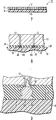
Der Bildsensor gemäß dieser Ausführungsform umfasst eine Halbleiterplatte
Die ersten Elektroden
CdTe und CdZnTe sind im allgemeinen brüchig bzw. spröde und für Menschen schädlich. Im Hinblick darauf werden die Löcher durch das spezielle Verfahren hergestellt, das später beschrieben wird.CdTe and CdZnTe are generally fragile or brittle and harmful to humans. in the In view of this, the holes are made by the special method which will be described later.
Die ersten Elektroden
In
Das Sensorelement
Das IC-Substrat
Alle Anoden
Das IC-Substrat
Die auf dem IC-Substrat
Die zwischen der CdTe-Platte
Jeder Stifthöcker-Verbindungsabschnitt
Die Indiumschicht
Die Isolierschicht
Der Bildsensor
Der Bildsensor
Wenn eine Spannung an jedes Sensorelement
Bei dem Bildsensor
Die elektrischen Drähte bzw. Zuleitungen können von den ersten Elektroden
(Verfahren zur Herstellung des Bildsensors)(Method of Manufacturing the Image Sensor)
Ein Verfahren zur Herstellung des Bildsensors
CdTe und CdZnTe und andere zusammengesetzte Halbleiter sind für den Menschen schädliche Substanzen. Wenn mit den ersten Elektroden
Dieses Verfahren löst diese Probleme. Es verhindert Splitterbildung und Rissbildung. Es ist sicher und unterstützt die Massenproduktion.This method solves these problems. It prevents splintering and cracking. It is safe and supports mass production.
Die Schutzschichten sind zwei Schichten mit einer vorbestimmten Dicke. Eine wird auf die obere Seite der CdTe-Platte und die andere auf die untere Seite der CdTe-Platte gelegt. Die Schutzschichten weisen die Funktion auf, die Entstehung der Splitterbildung und der Rissbildung beim Entwickeln in der CdTe-Platte zu verhindern, wenn eine Mehrzahl von Löchern in der Platte in Ausrichtung mit den ersten Elektroden
Als nächstes wird die somit durch die Schutzschichten geschützte CdTe-Platte in Wasser eingetaucht, und Löcher einer vorbestimmten Größe werden in der Platte in Ausrichtung mit den ersten Elektroden
Dann werden die Schutzschichten von der CdTe-Platte entfernt (Schritt S3).Then, the protective layers are removed from the CdTe plate (step S3).
Danach wird die Metallisierung in den Löchern ausgeführt, wobei erste Elektroden
Schließlich werden zweite Elektroden
Die Erfinder dieser Erfindung führten Experimente durch. Gute Ergebnisse wurden bei Schritt S1 insbesondere erreicht, wenn die auf den oberen bzw. unteren Seiten der CdTe-Platte aufgebrachten Schutzschichten jeweils eine Dicke aufwiesen, die gleich oder größer der Hälfte der Dicke der CdTe-Platte war. Ferner tritt weder Splitterbildung noch Rissbildung auf, selbst wenn die Löcher mit einem Abstand von 100 Mikron mit einem Bohrer mit einem Durchmesser von 50 Mikron hergestellt wurden. Somit konnte ein guter Bildsensor
Das oben beschriebene Herstellungsverfahren kann Splitterbildung und Rissbildung verhindern, wenn die Platte aus CdTe, CdZnTe, GaAs, HgIn, HgIz oder irgendeinem anderen zusammengesetzten Halbleiter hergestellt wird, der spröde oder brüchig und für Menschen schädlich ist. Daher kann mit dem Verfahren der Bildsensor sowohl sicher als auch einfach hergestellt werden.The manufacturing method described above can prevent chipping and cracking when the board is made of CdTe, CdZnTe, GaAs, HgIn, HgIz or any other compound semiconductor which is brittle or fragile and harmful to humans. Therefore, the method can make the image sensor both safe and easy.
(Zweite Ausführungsform)Second Embodiment
Die zweite Ausführungsform wird nun beschrieben. Die zweite Ausführungsform ist eine Bildsensoreinheit (d. h. ein dreidimensionaler Bildsensor)
Wie es
Wie in
Die Vorverstärkereinheit
Die Abtastverstärkereinheit
Die dreidimensionale Bildsensoreinheit
Die Erfindung ist nicht auf die in
Die Sensorelemente
Industrielle AnwendbarkeitIndustrial applicability
Die Erfindung kann einen Bildsensor, der Strahlen, sogar diejenigen des harten Röntgenstrahlenergiebandes, mit hoher Empfindlichkeit und hoher Auflösung erfassen kann, und ein Verfahren zur Herstellung eines derartigen Bildsensors bereitstellen.The invention can provide an image sensor capable of detecting beams, even those of the hard X-ray energy band, with high sensitivity and high resolution, and a method of manufacturing such an image sensor.
Claims (16)
Applications Claiming Priority (3)
| Application Number | Priority Date | Filing Date | Title |
|---|---|---|---|
| JP2001-339711 | 2001-11-05 | ||
| JP2001339711A JP4397012B2 (en) | 2001-11-05 | 2001-11-05 | Semiconductor image sensor having hole-type electrode and manufacturing method thereof |
| PCT/JP2002/011524 WO2003041175A1 (en) | 2001-11-05 | 2002-11-05 | Image sensor and its manufacturing method |
Publications (2)
| Publication Number | Publication Date |
|---|---|
| DE10296322T5 DE10296322T5 (en) | 2004-08-19 |
| DE10296322B4 true DE10296322B4 (en) | 2013-02-21 |
Family
ID=19154020
Family Applications (1)
| Application Number | Title | Priority Date | Filing Date |
|---|---|---|---|
| DE10296322T Expired - Fee Related DE10296322B4 (en) | 2001-11-05 | 2002-11-05 | Image sensor and method of making the same |
Country Status (4)
| Country | Link |
|---|---|
| US (1) | US7042008B2 (en) |
| JP (1) | JP4397012B2 (en) |
| DE (1) | DE10296322B4 (en) |
| WO (1) | WO2003041175A1 (en) |
Families Citing this family (7)
| Publication number | Priority date | Publication date | Assignee | Title |
|---|---|---|---|---|
| JP5135651B2 (en) * | 2001-05-15 | 2013-02-06 | 株式会社アクロラド | Semiconductor radiation detector |
| JP3897245B2 (en) | 2002-04-24 | 2007-03-22 | 三菱重工業株式会社 | Gamma ray source distance measuring device using multilayer radiation detector. |
| JP4238373B2 (en) | 2002-05-20 | 2009-03-18 | 三菱重工業株式会社 | Radiation source position detection method and radiation source position detection system |
| JP5106822B2 (en) * | 2006-10-27 | 2012-12-26 | 三菱重工業株式会社 | Semiconductor device, inspection device, and manufacturing method of semiconductor device |
| CN101903802B (en) * | 2007-12-20 | 2013-09-11 | 皇家飞利浦电子股份有限公司 | Direct conversion detector |
| CN102403232B (en) * | 2011-11-29 | 2013-05-08 | 中国电子科技集团公司第五十八研究所 | Process for total dose radiation hardening of factory region |
| JP2017092419A (en) * | 2015-11-17 | 2017-05-25 | 株式会社島津製作所 | Semiconductor detector |
Citations (1)
| Publication number | Priority date | Publication date | Assignee | Title |
|---|---|---|---|---|
| JP2001291853A (en) * | 2000-04-04 | 2001-10-19 | Hamamatsu Photonics Kk | Semiconductor energy detecting element |
Family Cites Families (6)
| Publication number | Priority date | Publication date | Assignee | Title |
|---|---|---|---|---|
| JPH08115946A (en) * | 1994-10-13 | 1996-05-07 | Matsushita Electric Ind Co Ltd | Flip chip mounting method |
| JPH08160147A (en) * | 1994-12-09 | 1996-06-21 | Japan Energy Corp | Semiconductor radiation detector |
| JP3243956B2 (en) * | 1995-02-03 | 2002-01-07 | 松下電器産業株式会社 | Semiconductor device and manufacturing method thereof |
| JPH1022337A (en) * | 1996-07-04 | 1998-01-23 | Hitachi Ltd | Semiconductor chip bonding method |
| JP3587991B2 (en) * | 1998-08-03 | 2004-11-10 | シャープ株式会社 | Two-dimensional image detector and manufacturing method thereof |
| JP4653336B2 (en) * | 2001-04-18 | 2011-03-16 | 浜松ホトニクス株式会社 | Energy ray detector and apparatus |
-
2001
- 2001-11-05 JP JP2001339711A patent/JP4397012B2/en not_active Expired - Lifetime
-
2002
- 2002-11-05 DE DE10296322T patent/DE10296322B4/en not_active Expired - Fee Related
- 2002-11-05 WO PCT/JP2002/011524 patent/WO2003041175A1/en not_active Ceased
-
2003
- 2003-08-08 US US10/636,616 patent/US7042008B2/en not_active Expired - Fee Related
Patent Citations (1)
| Publication number | Priority date | Publication date | Assignee | Title |
|---|---|---|---|---|
| JP2001291853A (en) * | 2000-04-04 | 2001-10-19 | Hamamatsu Photonics Kk | Semiconductor energy detecting element |
Also Published As
| Publication number | Publication date |
|---|---|
| JP2003142670A (en) | 2003-05-16 |
| US20040026758A1 (en) | 2004-02-12 |
| WO2003041175A1 (en) | 2003-05-15 |
| JP4397012B2 (en) | 2010-01-13 |
| US7042008B2 (en) | 2006-05-09 |
| DE10296322T5 (en) | 2004-08-19 |
Similar Documents
| Publication | Publication Date | Title |
|---|---|---|
| DE69313743T2 (en) | Image sensor for ionizing radiation | |
| DE3813079C2 (en) | ||
| DE69410959T2 (en) | Solid-state radiation detector panel with light-sensitive detectors arranged in a matrix, arranged in such a way that edge effects between the elements are minimized | |
| DE69737492T2 (en) | Process for the preparation of a photosensitive component with back radiation incidence | |
| DE10307752B4 (en) | X-ray detector | |
| DE102014225396B3 (en) | Sensor board for a detector module and method for its production | |
| DE10142531A1 (en) | Sensor arrangement of light and / or X-ray sensitive sensors | |
| DE102016221481B4 (en) | Radiation detector with an intermediate layer | |
| DE102012202500B4 (en) | Digital X-ray detector and method for correcting an X-ray image | |
| DE102007062891A1 (en) | Construction of CT detector modules | |
| DE102014221829B4 (en) | Method for producing a sensor board for a detector module and detector module produced thereby | |
| DE102011108876B4 (en) | Direct conversion X-ray detector with radiation protection for the electronics | |
| DE69825808T2 (en) | Photoelectric conversion device | |
| DE10244177A1 (en) | Photosensitive screen for taking X-ray pictures has top fluorescent layer on contact layer on top of photosensor array with individual contacts on substrate with further contacts to circuit elements | |
| DE10296322B4 (en) | Image sensor and method of making the same | |
| DE102005003378A1 (en) | Device for the detection of ionizing radiation | |
| DE4310622A1 (en) | Device for micro-imaging using ionizing radiation | |
| DE102008063323A1 (en) | Radiation detector, light detector assembly, manufacturing method and imaging system | |
| DE112016003614B4 (en) | Bond pads with different sized openings | |
| DE102004052452B4 (en) | Radiation detector for detecting radiation | |
| DE19618465C1 (en) | Radiation detector array for X=ray or gamma radiation | |
| DE4025427A1 (en) | DETECTOR ARRANGEMENT FOR DETECTING X-RAY RADIATION AND METHOD FOR THE PRODUCTION THEREOF | |
| EP3663806B1 (en) | Photon detector, method for producing a photon detector and x-ray device | |
| EP1059671A2 (en) | X-ray image sensor | |
| DE102011077058A1 (en) | Radiation detector and imaging system |
Legal Events
| Date | Code | Title | Description |
|---|---|---|---|
| 8110 | Request for examination paragraph 44 | ||
| R018 | Grant decision by examination section/examining division | ||
| R020 | Patent grant now final |
Effective date: 20130522 |
|
| R119 | Application deemed withdrawn, or ip right lapsed, due to non-payment of renewal fee |