DE102018105869A1 - Method for producing a semiconductor-based pressure sensor with a measuring membrane etched from a substrate - Google Patents
Method for producing a semiconductor-based pressure sensor with a measuring membrane etched from a substrate Download PDFInfo
- Publication number
- DE102018105869A1 DE102018105869A1 DE102018105869.1A DE102018105869A DE102018105869A1 DE 102018105869 A1 DE102018105869 A1 DE 102018105869A1 DE 102018105869 A DE102018105869 A DE 102018105869A DE 102018105869 A1 DE102018105869 A1 DE 102018105869A1
- Authority
- DE
- Germany
- Prior art keywords
- substrate
- recess
- semiconductor
- etching process
- pressure sensor
- Prior art date
- Legal status (The legal status is an assumption and is not a legal conclusion. Google has not performed a legal analysis and makes no representation as to the accuracy of the status listed.)
- Ceased
Links
- 239000000758 substrate Substances 0.000 title claims abstract description 56
- 239000004065 semiconductor Substances 0.000 title claims abstract description 37
- 239000012528 membrane Substances 0.000 title claims abstract description 32
- 238000004519 manufacturing process Methods 0.000 title claims abstract description 5
- 238000000034 method Methods 0.000 claims abstract description 51
- 238000005530 etching Methods 0.000 claims abstract description 47
- 239000000126 substance Substances 0.000 claims abstract description 7
- 238000005304 joining Methods 0.000 claims abstract description 3
- XUIMIQQOPSSXEZ-UHFFFAOYSA-N Silicon Chemical compound [Si] XUIMIQQOPSSXEZ-UHFFFAOYSA-N 0.000 claims description 25
- 229910052710 silicon Inorganic materials 0.000 claims description 25
- 239000010703 silicon Substances 0.000 claims description 21
- 239000000463 material Substances 0.000 claims description 16
- 230000013011 mating Effects 0.000 claims description 4
- 239000002210 silicon-based material Substances 0.000 claims 1
- KWYUFKZDYYNOTN-UHFFFAOYSA-M Potassium hydroxide Chemical compound [OH-].[K+] KWYUFKZDYYNOTN-UHFFFAOYSA-M 0.000 description 29
- 230000001154 acute effect Effects 0.000 description 5
- 230000001419 dependent effect Effects 0.000 description 5
- 238000001020 plasma etching Methods 0.000 description 3
- 208000013201 Stress fracture Diseases 0.000 description 2
- 238000011161 development Methods 0.000 description 2
- 230000000694 effects Effects 0.000 description 2
- 230000002411 adverse Effects 0.000 description 1
- 238000010923 batch production Methods 0.000 description 1
- 230000009172 bursting Effects 0.000 description 1
- 238000000576 coating method Methods 0.000 description 1
- 239000013078 crystal Substances 0.000 description 1
- 230000008021 deposition Effects 0.000 description 1
- 238000001514 detection method Methods 0.000 description 1
- 238000011156 evaluation Methods 0.000 description 1
- 238000002513 implantation Methods 0.000 description 1
- 238000002955 isolation Methods 0.000 description 1
- 238000005259 measurement Methods 0.000 description 1
- 230000003647 oxidation Effects 0.000 description 1
- 238000007254 oxidation reaction Methods 0.000 description 1
- 238000012545 processing Methods 0.000 description 1
Images
Classifications
-
- G—PHYSICS
- G01—MEASURING; TESTING
- G01L—MEASURING FORCE, STRESS, TORQUE, WORK, MECHANICAL POWER, MECHANICAL EFFICIENCY, OR FLUID PRESSURE
- G01L9/00—Measuring steady of quasi-steady pressure of fluid or fluent solid material by electric or magnetic pressure-sensitive elements; Transmitting or indicating the displacement of mechanical pressure-sensitive elements, used to measure the steady or quasi-steady pressure of a fluid or fluent solid material, by electric or magnetic means
- G01L9/0041—Transmitting or indicating the displacement of flexible diaphragms
- G01L9/0042—Constructional details associated with semiconductive diaphragm sensors, e.g. etching, or constructional details of non-semiconductive diaphragms
- G01L9/0047—Diaphragm with non uniform thickness, e.g. with grooves, bosses or continuously varying thickness
-
- B—PERFORMING OPERATIONS; TRANSPORTING
- B81—MICROSTRUCTURAL TECHNOLOGY
- B81B—MICROSTRUCTURAL DEVICES OR SYSTEMS, e.g. MICROMECHANICAL DEVICES
- B81B3/00—Devices comprising flexible or deformable elements, e.g. comprising elastic tongues or membranes
- B81B3/0064—Constitution or structural means for improving or controlling the physical properties of a device
- B81B3/0067—Mechanical properties
- B81B3/0072—For controlling internal stress or strain in moving or flexible elements, e.g. stress compensating layers
-
- G—PHYSICS
- G01—MEASURING; TESTING
- G01L—MEASURING FORCE, STRESS, TORQUE, WORK, MECHANICAL POWER, MECHANICAL EFFICIENCY, OR FLUID PRESSURE
- G01L9/00—Measuring steady of quasi-steady pressure of fluid or fluent solid material by electric or magnetic pressure-sensitive elements; Transmitting or indicating the displacement of mechanical pressure-sensitive elements, used to measure the steady or quasi-steady pressure of a fluid or fluent solid material, by electric or magnetic means
- G01L9/0041—Transmitting or indicating the displacement of flexible diaphragms
- G01L9/0051—Transmitting or indicating the displacement of flexible diaphragms using variations in ohmic resistance
- G01L9/0052—Transmitting or indicating the displacement of flexible diaphragms using variations in ohmic resistance of piezoresistive elements
- G01L9/0054—Transmitting or indicating the displacement of flexible diaphragms using variations in ohmic resistance of piezoresistive elements integral with a semiconducting diaphragm
-
- B—PERFORMING OPERATIONS; TRANSPORTING
- B81—MICROSTRUCTURAL TECHNOLOGY
- B81B—MICROSTRUCTURAL DEVICES OR SYSTEMS, e.g. MICROMECHANICAL DEVICES
- B81B2201/00—Specific applications of microelectromechanical systems
- B81B2201/02—Sensors
- B81B2201/0264—Pressure sensors
-
- B—PERFORMING OPERATIONS; TRANSPORTING
- B81—MICROSTRUCTURAL TECHNOLOGY
- B81C—PROCESSES OR APPARATUS SPECIALLY ADAPTED FOR THE MANUFACTURE OR TREATMENT OF MICROSTRUCTURAL DEVICES OR SYSTEMS
- B81C2203/00—Forming microstructural systems
- B81C2203/03—Bonding two components
- B81C2203/033—Thermal bonding
- B81C2203/036—Fusion bonding
Landscapes
- Engineering & Computer Science (AREA)
- Physics & Mathematics (AREA)
- General Physics & Mathematics (AREA)
- Mechanical Engineering (AREA)
- Computer Hardware Design (AREA)
- Microelectronics & Electronic Packaging (AREA)
- Chemical & Material Sciences (AREA)
- Analytical Chemistry (AREA)
- Pressure Sensors (AREA)
- Measuring Fluid Pressure (AREA)
Abstract
Verfahren zum Herstellen eines halbleiterbasierten Drucksensors mit einer aus einem Substrat (1) geätzten Messmembran (2), umfassend die folgenden Schritte:- Bereitstellen des Substrats (1);- Erzeugen der Messmembran (2) durch Ätzen des Substrates (1) mittels eines zweistufigen Ätzprozesses, wobei der zweistufige Ätzprozess vorsieht, dass in einem ersten Schritt ein anisotroper Ätzprozess zum Erzeugen einer ersten Aussparung (4) mit rechtwinkligen Seitenwänden (4a) und in einem zweiten dem ersten Schritt nachfolgenden Schritt ein anisotroper nasschemischer KOH-Ätzprozess zur Erzeugung einer an die erste Aussparung (4) anschließenden zweiten Aussparung (5) mit konisch verjüngenden Seitenwänden (5a) durchgeführt wird;- Fügen des Substrates (1) mit einem Gegenkörper (3), so dass ein an die Aussparungen (4, 5) angrenzendes randseitiges Verbindungselement (9) mit einem Randbereich des Gegenkörpers (3) gefügt wird, so dass ein Winkel von in etwa 90° zwischen den Seitenwänden der ersten Aussparung (4a) und einer Ebene, in der eine erste Oberfläche des Gegenkörpers (3aa) liegt, gebildet wird.Method for producing a semiconductor-based pressure sensor with a measuring membrane (2) etched from a substrate (1), comprising the following steps: - providing the substrate (1), - producing the measuring membrane (2) by etching the substrate (1) by means of a two-stage process Etching process, wherein the two-stage etching process provides that in an initial step, an anisotropic etching process for producing a first recess (4) with rectangular side walls (4a) and in a second step following the first step, an anisotropic wet-chemical KOH etching process for generating a to the first recess (4) adjoins the second recess (5) with conically tapering side walls (5a), - joining the substrate (1) with a counterbody (3), so that an edge-side connecting element (4, 5) adjoining the recesses (4, 5) 9) is joined with an edge region of the counter body (3), so that an angle of approximately 90 ° between the side walls the first recess (4a) and a plane in which a first surface of the counter body (3aa) is formed, is formed.
Description
Die Erfindung bezieht sich auf ein Verfahren zum Herstellen eines halbleiterbasierten Drucksensors mit einer aus einem Substrat geätzten Messmembran, einen halbleiterbasierten Drucksensor mit einer aus einem Substrat geätzten Messmembran erhältlich durch das Verfahren und ein halbleiterbasierter Drucksensor mit einer strukturierten Messmembran.The invention relates to a method for producing a semiconductor-based pressure sensor with a measuring membrane etched from a substrate, a semiconductor-based pressure sensor with a measuring membrane etched from a substrate obtainable by the method and a semiconductor-based pressure sensor with a structured measuring membrane.
Halbleiterbasierte Drucksensoren, die gelegentlich auch MEMS-Drucksensoren genannt werden, werden regelmäßig aus aufeinander angeordneten Lagen, insb. Siliziumlagen, aufgebaut, und unter Verwendung von in der Halbleitertechnologie üblichen Verfahren, wie z.B. Ätzprozessen, Oxidationsverfahren, Implantationsverfahren, Bondverfahren und/oder Beschichtungsverfahren hergestellt. Dabei werden die einzelnen Lagen, sowie ggfs. zwischen benachbarten Lagen vorgesehene Verbindungsschichten, z.B. Isolationsschichten, entsprechend der ihnen im Sensor zukommenden Funktion präpariert bzw. strukturiert.Semiconductor-based pressure sensors, sometimes referred to as MEMS pressure sensors, are regularly constructed of stacked layers, especially silicon layers, and are fabricated using techniques commonly used in semiconductor technology, such as silicon deposition. Etching processes, oxidation method, implantation method, bonding method and / or coating method produced. In this case, the individual layers, as well as possibly provided between adjacent layers connecting layers, e.g. Isolation layers, according to their function in the sensor prepared or structured.
Derartige halbleiterbasierte Drucksensoren umfassen für gewöhnlich Komponenten, die einer mechanischen Belastung ausgesetzt sein können. Ein Beispiel hierfür sind Funktionselemente von in den Drucksensoren integrierten elektromechanischen Wandlern, die einer von der zu erfassenden Messgröße abhängigen mechanischen Belastung ausgesetzt werden, die vom Wandler in eine von der Messgröße abhängige elektrische Größe umwandelt wird.Such semiconductor-based pressure sensors usually include components which may be subject to mechanical stress. An example of this are functional elements of electromechanical transducers integrated in the pressure sensors, which are exposed to a mechanical load which is dependent on the measured variable to be detected and which is converted by the transducer into an electrical variable dependent on the measured variable.
Mechanische Belastungen bewirken zwangsläufig Spannungen die einzelne Strukturelemente und/oder mit einzelnen Strukturelementen verbundene weitere Strukturelemente mechanisch beanspruchen. Das stellt solange kein Problem dar, wie die Belastungen eine für den Sensor vorgegebene häufig als Überlastfestigkeit bezeichnete Belastungsgrenze nicht überschreiten. Es kommt jedoch in der Praxis immer wieder vor, dass Sensoren Überbelastungen ausgesetzt werden.Mechanical loads inevitably cause stresses mechanically stress the individual structural elements and / or other structural elements associated with individual structural elements. This poses no problem as long as the loads do not exceed a load limit, which is often specified for the sensor as an overload resistance. However, it often happens in practice that sensors are subjected to overloading.
Die Gefahr einer Überbelastung ist insb. bei Differenzdrucksensoren besonders groß, die dazu eingesetzt werden Druckdifferenzen Δp zwischen zwei im Vergleich zur Druckdifferenz Δp großen Drücken p1, p2 zu messen. Da diese Sensoren empfindlich genug sein müssen, um die dem kleineren der beiden Drücken entsprechenden Systemdruck überlagerte Druckdifferenz Δp messtechnisch erfassen zu können, stellen vor allem einseitige Überlasten, bei denen nur eine Seite einer Messmembran des Differenzdrucksensors mit dem Systemdruck beaufschlagt wird, dem kein auf die gegenüberliegenden Seite der Messmembran einwirkender Gegendruck entgegenwirkt, ein Problem dar.The risk of overloading is esp. In differential pressure sensors particularly large, which are used to measure pressure differences Δp between two compared to the pressure difference Ap large pressures p1, p2. Since these sensors must be sensitive enough to be able to measure the pressure difference Δp superimposed on the smaller system pressure corresponding to the two pressures, one-sided overloads, in which only one side of a measuring diaphragm of the differential pressure sensor is subjected to the system pressure, are not affected by the system pressure counteracts the counter-pressure acting on the opposite side of the measuring diaphragm, a problem.
Dabei sind Sensoren, die Bereiche mit spitzen Winkeln aufweisen, besonders empfindlich gegenüber mechanischen Belastungen, da sich an spitzen Winkeln Kerbspannungen konzentrieren, die im Falle einer Überbelastung Spannungsrisse oder sogar Spannungsbrüche verursachen können.In this case, sensors having areas with acute angles, are particularly sensitive to mechanical stress, because at acute angles focus notch stresses that can cause stress cracks or even stress fractures in the event of overload.
Ein Beispiel hierfür sind piezoresistive Drucksensoren, die eine mit einem zu messenden Druck beaufschlagbare Messmembran aufweisen. Diese Drucksensoren werden regelmäßig hergestellt, in dem in einen Siliziumwafer mittels eines anisotropen Ätzverfahren, z.B. eines mit Kaliumhydroxid (KOH) ausgeführten anisotropen Ätzverfahren, eine Ausnehmung eingeätzt wird. Dabei bildet ein die Ausnehmung umgebender Rand einen Träger, der die Messmembran trägt. Ein derartig geätzter Wafer wird an einer Grenzfläche, die sich auf der der Messmembran abgewandten Seite des Siliziumwafers befindet, anschließend mit einem Gegenkörper, bspw. in Form eines weiteren Siliziumwafers, gefügt. Hierdurch entsteht an der Grenzfläche ein spitzer Winkel von typischerweise ca. 54,7°, an welchem bei entsprechender Druckbelastung Kerbspannungen auftreten, so dass es in einem genügend großen Belastungsfall, bspw. in dem Überlastfall, zu Spannungsrissen bzw. Spannungsbrüchen kommen kann.An example of this are piezoresistive pressure sensors, which have a measuring membrane which can be acted upon by a pressure to be measured. These pressure sensors are regularly made by placing them in a silicon wafer by means of an anisotropic etching process, e.g. of an anisotropic etching process carried out with potassium hydroxide (KOH), a recess is etched. In this case, an edge surrounding the recess forms a carrier, which carries the measuring diaphragm. Such an etched wafer is then joined to an opposing body, for example in the form of another silicon wafer, at an interface which is located on the side of the silicon wafer facing away from the measuring membrane. This results in an acute angle of typically about 54.7 °, at which an appropriate pressure load notch stresses occur at the interface, so that in a sufficiently large load case, for example. In the overload case, can lead to stress cracks or stress fractures.
Der Erfindung liegt somit die Aufgabe zugrunde, die bei Drucksensoren an spitzen Winkeln auftretende Kerbspannung zu minimieren.The invention is therefore based on the object to minimize the notch stress occurring at pressure sensors at acute angles.
Die Aufgabe wird erfindungsgemäß gelöst durch das Verfahren gemäß Patentanspruch 1, den halbleiterbasierten Drucksensor erhältlich durch das Verfahren gemäß Patentanspruch 5 und den halbleiterbasierten Drucksensor gemäß Patentanspruch 6.The object is achieved by the method according to claim 1, the semiconductor-based pressure sensor obtainable by the method according to
Das erfindungsgemäße Verfahren zum Herstellen eines halbleiterbasierten, insbesondere piezoresistiven Drucksensors mit einer aus einem Substrat geätzten Messmembran, umfasst die folgenden Schritte:
- - Bereitstellen des Substrats, welches ein Halbleitermaterial, insbesondere ein Silizium aufweist;
- - Erzeugen der Messmembran durch Ätzen des Substrates mittels eines zweistufigen Ätzprozesses, wobei der zweistufige Ätzprozess vorsieht, dass in einem ersten Schritt ein anisotroper Ätzprozess zum Erzeugen einer ersten Aussparung mit in Bezug zu einer ersten Oberfläche des Substrates im Wesentlichen rechtwinkligen Seitenwänden und in einem zweiten dem ersten Schritt nachfolgenden Schritt ein anisotroper nasschemischer KOH-Ätzprozess zur Erzeugung einer an die erste Aussparung anschließenden zweiten Aussparung mit sich zu einer der ersten Oberfläche abgewandten zweiten Oberfläche des Substrates hin konisch verjüngenden Seitenwänden durchgeführt wird;
- - Fügen des Substrates mit der geätzten Messmembran mit einem Gegenkörper, insbesondere einen ein Halbleitermaterial, ganz besonders einen ein Silizium aufweisenden Gegenkörper, wobei das Substrat mit dem Gegenkörper derartig gefügt wird, dass ein an die erste und zweite Aussparung angrenzendes randseitiges Verbindungselement mit einem entsprechenden Randbereich des Gegenkörpers gefügt wird, so dass ein Winkel von in etwa 90° zwischen den Seitenwänden der ersten Aussparung und einer Ebene, in der eine erste Oberfläche des Gegenkörpers liegt, gebildet wird.
- - Providing the substrate, which comprises a semiconductor material, in particular a silicon;
- Generating the measuring diaphragm by etching the substrate by means of a two-stage etching process, wherein the two-stage etching process provides, in a first step, an anisotropic etching process for producing a first recess with side walls substantially perpendicular to a first surface of the substrate and in a second one the first step following an anisotropic wet-chemical KOH etching process Producing a second recess adjoining the first recess with side walls facing away from the first surface facing away from the second surface of the substrate is performed conically tapering side walls;
- - Including the substrate with the etched measuring membrane with a counter body, in particular a semiconductor material, especially a silicon-containing counter body, wherein the substrate is joined to the counter body such that an adjacent to the first and second recess edge-side connecting element with a corresponding edge region is added to the counter body, so that an angle of approximately 90 ° between the side walls of the first recess and a plane in which a first surface of the counter body is formed, is formed.
Erfindungsgemäß wird zur Erzeugung der Messmembran eine Kombination aus einem anisotropen Ätzprozess zur Erzeugung von senkrechten Seitenwänden und einem anisotropen nasschemischen KOH-Ätzprozess angewandt, wobei zuerst mittels des anisotropen Ätzprozesses ein erster Teil der Ausnehmung bzw. eine erste Ausnehmung und anschließen mittels des anisotropen nasschemischen KOH-Ätzprozesses ein zweiter Teil der Ausnehmung bzw. eine zweite Ausnehmung erzeugt wird. Hierdurch können die für gewöhnlich entstehenden spitzen Winkel vermieden werden, indem der entsprechende Winkel von ca. 54,7° auf ca. 90° erhöht wird, so dass die nachteiligen Kerbspannungen reduziert werden. Gemäß dem erfindungsgemäßen Verfahren ist weiterhin im zweiten Schritt die Nutzung des KOH-Ätzprozesses mit hoher reproduzierbarer Strukturtreue und als kostengünstiger Batchprozess möglich.According to the invention, a combination of an anisotropic etching process for producing vertical sidewalls and an anisotropic wet-chemical KOH etching process is used to produce the measurement membrane, wherein first by means of the anisotropic etching process a first part of the recess or a first recess and connect by means of the anisotropic wet-chemical KOH Etching process, a second part of the recess or a second recess is generated. As a result, the usually resulting acute angle can be avoided by the corresponding angle of about 54.7 ° is increased to about 90 °, so that the adverse notch stresses are reduced. According to the method of the invention, the use of the KOH etching process with high reproducible structure fidelity and as a cost-effective batch process is furthermore possible in the second step.
Eine erste vorteilhafte Ausführungsform des erfindungsgemäßen Verfahrens sieht vor, dass das Substrat und/oder der Gegenkörper in Form eines Halbleiter-Wafers, insbesondere eines Silizium-Wafers, mit einer Materialstärke von einigen hundert Mikrometer bereitgestellt wird.A first advantageous embodiment of the method according to the invention provides that the substrate and / or the counter-body is provided in the form of a semiconductor wafer, in particular a silicon wafer, with a material thickness of a few hundred micrometers.
Eine weitere vorteilhafte Ausführungsform des erfindungsgemäßen Verfahrens sieht vor, dass eine Ätztiefe der ersten und zweiten Aussparung derartig gewählt wird, dass die Messmembran eine Materialstärke im Bereich von 10-250 Mikrometern, bevorzugt im Bereich von 15-200 Mikrometern, ganz besonders bevorzugt im Bereich von 20-150 Mikrometern aufweist.A further advantageous embodiment of the method according to the invention provides that an etching depth of the first and second recess is chosen such that the measuring membrane has a material thickness in the range of 10-250 micrometers, preferably in the range of 15-200 micrometers, most preferably in the range of 20-150 microns has.
Wiederum eine weitere vorteilhafte Ausführungsform sieht vor, dass für den anisotropen Ätzprozess ein reaktives Ionenätzverfahren oder eine davon abgewandelte Variante, insbesondere ein reaktives lonentiefenätzverfahren, verwendet wird.Yet another advantageous embodiment provides that a reactive ion etching process or a variant modified therefrom, in particular a reactive ion etching process, is used for the anisotropic etching process.
Die Erfindung betrifft weiterhin einen halbleiterbasierten, insbesondere piezoresistiven Drucksensor mit einer aus einem Substrat geätzten Messmembran erhältlich durch das zuvor beschriebene Verfahren.The invention further relates to a semiconductor-based, in particular piezoresistive pressure sensor with a measuring membrane etched from a substrate obtainable by the method described above.
Die Erfindung betrifft weiterhin auch einen halbleiterbasierten, insbesondere piezoresistiven Drucksensors mit einer strukturierten Messmembran aufweisend:
- - ein Substrat, welches ein Halbleitermaterial, insbesondere ein Silizium aufweist;
- - eine in dem Substrat befindliche von einer ersten Oberfläche des Substrates ausgehende erste Aussparung mit Seitenwänden, die in Bezug zu einer Ebene, in der die erste Oberfläche des Substrates liegt, im Wesentlichen rechtwinklig sind;
- - eine in dem Substrat an die erste Aussparung angrenzende zweite Aussparung mit sich zu einer der ersten Oberfläche abgewandten zweiten Oberfläche des Substrates hin konisch verjüngenden Seitenwänden;
- - einen Gegenkörper, welcher insbesondere ein Halbleitermaterial, ganz besonders ein Silizium aufweist, wobei der Gegenkörper mit dem Substrat derartig gefügt ist, dass ein an die erste und zweite Aussparung angrenzendes randseitig umlaufendes Verbindungselement mit einem entsprechenden Randbereich des Gegenkörpers gefügt ist, so dass sich ein Winkel von in etwa 90° zwischen den Seitenwänden der ersten Aussparung und einer Ebene, in der eine erste Oberfläche des Gegenkörpers liegt, bildet.
- a substrate comprising a semiconductor material, in particular a silicon;
- an in-substrate first recess extending from a first surface of the substrate having sidewalls substantially rectangular with respect to a plane in which the first surface of the substrate is located;
- - A in the substrate adjacent to the first recess second recess with to the first surface facing away from the second surface of the substrate towards conically tapered side walls;
- a mating body, which in particular has a semiconductor material, especially a silicon, wherein the mating body is joined to the substrate in such a way that a connecting element bordering the first and second recesses is joined to a corresponding edge area of the mating body, so that a Angle of approximately 90 ° between the side walls of the first recess and a plane in which a first surface of the counter body is formed.
Eine vorteilhafte Weiterbildung des erfindungsgemäßen halbleiterbasierten Drucksensors sieht vor, dass das Substrat und/oder der Gegenkörper ein Halbleiter-Wafer, insbesondere eine Silizium-Wafer, mit einer Materialstärke von einigen hundert Mikrometer umfasst.An advantageous development of the semiconductor-based pressure sensor according to the invention provides that the substrate and / or the counter body comprises a semiconductor wafer, in particular a silicon wafer, with a material thickness of a few hundred micrometers.
Eine weitere vorteilhafte Weiterbildung des erfindungsgemäßen halbleiterbasierten Drucksensors sieht vor, dass eine Ätztiefe der ersten und zweiten Aussparung derartig bemessen ist, dass die Messmembran eine Materialstärke im Bereich von 10-250 Mikrometern, bevorzugt im Bereich von 15-200 Mikrometern, ganz besonders bevorzugt im Bereich von 20-150 Mikrometern aufweist.A further advantageous development of the semiconductor-based pressure sensor according to the invention provides that an etching depth of the first and second recess is dimensioned such that the measuring membrane has a material thickness in the range of 10-250 micrometers, preferably in the range of 15-200 micrometers, most preferably in the range of 20-150 microns.
Die Erfindung wird anhand der nachfolgenden Zeichnungen näher erläutert. Es zeigt:The invention will be explained in more detail with reference to the following drawings. It shows:
-
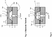
1 : einen Längsschnitt durch einen aus dem Stand der Technik bekannten halbleiterbasierten piezoresistiven Drucksensor, und1 FIG. 2: a longitudinal section through a semiconductor-based piezoresistive pressure sensor known from the prior art, and FIG -
2 : einen Längsschnitt durch ein Ausführungsbeispiel eines erfindungsgemäßen halbleiterbasierten piezoresistiven Drucksensors.2 : A longitudinal section through an embodiment of a semiconductor-based piezoresistive pressure sensor according to the invention.
Prinzipiell kann der halbleiterbasierte piezoresistive Drucksensor als Differenzdruck-, als Relativdruck- oder als Absolutdrucksensor ausgestaltet sein.In principle, the semiconductor-based piezoresistive pressure sensor can be configured as a differential pressure, relative pressure or absolute pressure sensor.
Zur Erfassung von Differenzdrücken wird eine erste Seite der Messmembran
Zur Erfassung von Relativdrücken wird die erste Seite der Messmembran
Zur Erfassung von Absolutdrücken ist die unter der Messmembran
Die resultierende Auslenkung der Messmembran
Der durch die KOH-Ätzung an der Fügeschicht
Um dies zu verhindern zeigt
Durch den zweistufigen Ätzprozess wird der Winkel zwischen den Seitenwänden der ersten Aussparung
BezugszeichenlisteLIST OF REFERENCE NUMBERS
- 11
- Substratsubstratum
- 1aa1aa
- Erste Oberfläche des SubstratsFirst surface of the substrate
- 1ab1ab
- Zweite Oberfläche des SubstratsSecond surface of the substrate
- 22
- Messmembranmeasuring membrane
- 33
- Gegenkörperagainst body
- 3aa3aa
- Erste Oberfläche des GegenkörpersFirst surface of the opposite body
- 3ab3ab
- Zweite Oberfläche des GegenkörpersSecond surface of the counter body
- 44
- Erste AussparungFirst recess
- 4a4a
- Seitenwände der ersten AussparungSide walls of the first recess
- 55
- Zweite AussparungSecond recess
- 5a5a
- Seitenwände der zweiten AussparungSide walls of the second recess
- 66
- FügeschichtAdd layer
- 77
- Widerstandselementresistive element
- 88th
- DruckeinlasskanalPressure inlet channel
- 99
- Verbindungselementconnecting member
- 1010
- Aussparung gemäß Stand der TechnikRecess according to the prior art
- 1111
- Druckkammerpressure chamber
- tt
- Ätztiefeetch depth
- αα
- Winkelangle
Claims (8)
Priority Applications (1)
| Application Number | Priority Date | Filing Date | Title |
|---|---|---|---|
| DE102018105869.1A DE102018105869A1 (en) | 2018-03-14 | 2018-03-14 | Method for producing a semiconductor-based pressure sensor with a measuring membrane etched from a substrate |
Applications Claiming Priority (1)
| Application Number | Priority Date | Filing Date | Title |
|---|---|---|---|
| DE102018105869.1A DE102018105869A1 (en) | 2018-03-14 | 2018-03-14 | Method for producing a semiconductor-based pressure sensor with a measuring membrane etched from a substrate |
Publications (1)
| Publication Number | Publication Date |
|---|---|
| DE102018105869A1 true DE102018105869A1 (en) | 2019-09-19 |
Family
ID=67774395
Family Applications (1)
| Application Number | Title | Priority Date | Filing Date |
|---|---|---|---|
| DE102018105869.1A Ceased DE102018105869A1 (en) | 2018-03-14 | 2018-03-14 | Method for producing a semiconductor-based pressure sensor with a measuring membrane etched from a substrate |
Country Status (1)
| Country | Link |
|---|---|
| DE (1) | DE102018105869A1 (en) |
Citations (2)
| Publication number | Priority date | Publication date | Assignee | Title |
|---|---|---|---|---|
| DE19723334A1 (en) * | 1997-06-04 | 1998-12-10 | Bosch Gmbh Robert | Pressure sensor |
| DE10126621A1 (en) * | 2000-06-05 | 2001-12-06 | Denso Corp | Semiconductor pressure sensor with a rounded corner part of a membrane for picking up pressure has a recess on a semiconductor substrate with a sidewall, a bottom wall acting as a membrane and a corner part with a bending radius |
-
2018
- 2018-03-14 DE DE102018105869.1A patent/DE102018105869A1/en not_active Ceased
Patent Citations (2)
| Publication number | Priority date | Publication date | Assignee | Title |
|---|---|---|---|---|
| DE19723334A1 (en) * | 1997-06-04 | 1998-12-10 | Bosch Gmbh Robert | Pressure sensor |
| DE10126621A1 (en) * | 2000-06-05 | 2001-12-06 | Denso Corp | Semiconductor pressure sensor with a rounded corner part of a membrane for picking up pressure has a recess on a semiconductor substrate with a sidewall, a bottom wall acting as a membrane and a corner part with a bending radius |
Similar Documents
| Publication | Publication Date | Title |
|---|---|---|
| EP2132547B1 (en) | Pressure sensor | |
| DE102013217726A1 (en) | Micromechanical component for a capacitive sensor device and method for producing a micromechanical component for a capacitive sensor device | |
| EP1876434A2 (en) | Device for measuring forces, in particular a pressure sensor and manufacturing method therefore | |
| DE69512544T2 (en) | Semiconductor pressure transducer with single crystal silicon membrane and single crystal strain gauges and manufacturing process therefor | |
| DE19750131C2 (en) | Micromechanical differential pressure sensor device | |
| EP3268304B1 (en) | Mems sensor, in particular a pressure sensor | |
| DE102007022852A1 (en) | Differential pressure sensor arrangement and corresponding manufacturing method | |
| CH684131A5 (en) | A process for producing accelerometers and acceleration sensor. | |
| WO2010108949A1 (en) | Pressure sensor | |
| DE102008043382A1 (en) | Component and method for its production | |
| DE102020120232A1 (en) | MEMS SENSOR | |
| DE102019201880B4 (en) | semiconductor pressure sensor | |
| WO2006072391A1 (en) | Force measuring device, especially pressure gauge, and associated production method | |
| DE102021212852A1 (en) | SEMICONDUCTOR PRESSURE SENSOR AND PRESSURE SENSING DEVICE | |
| DE102014118850A1 (en) | Pressure sensor for measuring a differential pressure and a system pressure | |
| DE102007014468A1 (en) | Pressure sensor chip | |
| DE102018105869A1 (en) | Method for producing a semiconductor-based pressure sensor with a measuring membrane etched from a substrate | |
| DE102007026450A1 (en) | Sensor e.g. pressure sensor, for pressure measurement, has substrate material and material staying in contact with one another in transition area, where substrate material exhibits nut, which is formed in area in substrate material | |
| DE102017109971A1 (en) | pressure sensor | |
| DE102005006666A1 (en) | Piezoelectric sensor e.g. for machine and automobile engineering, has thermo-sensor and amplifier circuit with temperature compensation | |
| DE102020202277A1 (en) | Micromechanical component for a stress sensor and manufacturing method for a micromechanical component for a stress sensor | |
| WO2010046149A1 (en) | Pressure sensor, particularly differential pressure sensor | |
| DE102009045158A1 (en) | Sensor arrangement and method for producing a sensor arrangement | |
| DE102018105868A1 (en) | Method for producing a semiconductor-based pressure sensor | |
| DE102016200701A1 (en) | Embedded structures for high glass strength and stable packaging |
Legal Events
| Date | Code | Title | Description |
|---|---|---|---|
| R163 | Identified publications notified | ||
| R082 | Change of representative |
Representative=s name: ANDRES, ANGELIKA, DIPL.-PHYS., DE |
|
| R012 | Request for examination validly filed | ||
| R016 | Response to examination communication | ||
| R002 | Refusal decision in examination/registration proceedings | ||
| R003 | Refusal decision now final |