DE102017220417A1 - Electronic module - Google Patents
Electronic module Download PDFInfo
- Publication number
- DE102017220417A1 DE102017220417A1 DE102017220417.6A DE102017220417A DE102017220417A1 DE 102017220417 A1 DE102017220417 A1 DE 102017220417A1 DE 102017220417 A DE102017220417 A DE 102017220417A DE 102017220417 A1 DE102017220417 A1 DE 102017220417A1
- Authority
- DE
- Germany
- Prior art keywords
- outer layer
- vias
- layer
- electronic module
- group
- Prior art date
- Legal status (The legal status is an assumption and is not a legal conclusion. Google has not performed a legal analysis and makes no representation as to the accuracy of the status listed.)
- Withdrawn
Links
Images

Classifications
-
- H—ELECTRICITY
- H05—ELECTRIC TECHNIQUES NOT OTHERWISE PROVIDED FOR
- H05K—PRINTED CIRCUITS; CASINGS OR CONSTRUCTIONAL DETAILS OF ELECTRIC APPARATUS; MANUFACTURE OF ASSEMBLAGES OF ELECTRICAL COMPONENTS
- H05K1/00—Printed circuits
- H05K1/02—Details
- H05K1/0213—Electrical arrangements not otherwise provided for
- H05K1/0216—Reduction of cross-talk, noise or electromagnetic interference
- H05K1/0218—Reduction of cross-talk, noise or electromagnetic interference by printed shielding conductors, ground planes or power plane
-
- H—ELECTRICITY
- H05—ELECTRIC TECHNIQUES NOT OTHERWISE PROVIDED FOR
- H05K—PRINTED CIRCUITS; CASINGS OR CONSTRUCTIONAL DETAILS OF ELECTRIC APPARATUS; MANUFACTURE OF ASSEMBLAGES OF ELECTRICAL COMPONENTS
- H05K1/00—Printed circuits
- H05K1/02—Details
- H05K1/0201—Thermal arrangements, e.g. for cooling, heating or preventing overheating
- H05K1/0203—Cooling of mounted components
- H05K1/0204—Cooling of mounted components using means for thermal conduction connection in the thickness direction of the substrate
- H05K1/0206—Cooling of mounted components using means for thermal conduction connection in the thickness direction of the substrate by printed thermal vias
-
- H—ELECTRICITY
- H05—ELECTRIC TECHNIQUES NOT OTHERWISE PROVIDED FOR
- H05K—PRINTED CIRCUITS; CASINGS OR CONSTRUCTIONAL DETAILS OF ELECTRIC APPARATUS; MANUFACTURE OF ASSEMBLAGES OF ELECTRICAL COMPONENTS
- H05K1/00—Printed circuits
- H05K1/18—Printed circuits structurally associated with non-printed electric components
- H05K1/181—Printed circuits structurally associated with non-printed electric components associated with surface mounted components
-
- H—ELECTRICITY
- H05—ELECTRIC TECHNIQUES NOT OTHERWISE PROVIDED FOR
- H05K—PRINTED CIRCUITS; CASINGS OR CONSTRUCTIONAL DETAILS OF ELECTRIC APPARATUS; MANUFACTURE OF ASSEMBLAGES OF ELECTRICAL COMPONENTS
- H05K1/00—Printed circuits
- H05K1/02—Details
- H05K1/0213—Electrical arrangements not otherwise provided for
- H05K1/0254—High voltage adaptations; Electrical insulation details; Overvoltage or electrostatic discharge protection ; Arrangements for regulating voltages or for using plural voltages
- H05K1/0257—Overvoltage protection
- H05K1/0259—Electrostatic discharge [ESD] protection
-
- H—ELECTRICITY
- H05—ELECTRIC TECHNIQUES NOT OTHERWISE PROVIDED FOR
- H05K—PRINTED CIRCUITS; CASINGS OR CONSTRUCTIONAL DETAILS OF ELECTRIC APPARATUS; MANUFACTURE OF ASSEMBLAGES OF ELECTRICAL COMPONENTS
- H05K2201/00—Indexing scheme relating to printed circuits covered by H05K1/00
- H05K2201/06—Thermal details
- H05K2201/066—Heatsink mounted on the surface of the printed circuit board [PCB]
-
- H—ELECTRICITY
- H05—ELECTRIC TECHNIQUES NOT OTHERWISE PROVIDED FOR
- H05K—PRINTED CIRCUITS; CASINGS OR CONSTRUCTIONAL DETAILS OF ELECTRIC APPARATUS; MANUFACTURE OF ASSEMBLAGES OF ELECTRICAL COMPONENTS
- H05K2201/00—Indexing scheme relating to printed circuits covered by H05K1/00
- H05K2201/07—Electric details
- H05K2201/0707—Shielding
- H05K2201/0715—Shielding provided by an outer layer of PCB
-
- H—ELECTRICITY
- H05—ELECTRIC TECHNIQUES NOT OTHERWISE PROVIDED FOR
- H05K—PRINTED CIRCUITS; CASINGS OR CONSTRUCTIONAL DETAILS OF ELECTRIC APPARATUS; MANUFACTURE OF ASSEMBLAGES OF ELECTRICAL COMPONENTS
- H05K2201/00—Indexing scheme relating to printed circuits covered by H05K1/00
- H05K2201/07—Electric details
- H05K2201/0707—Shielding
- H05K2201/0723—Shielding provided by an inner layer of PCB
-
- H—ELECTRICITY
- H05—ELECTRIC TECHNIQUES NOT OTHERWISE PROVIDED FOR
- H05K—PRINTED CIRCUITS; CASINGS OR CONSTRUCTIONAL DETAILS OF ELECTRIC APPARATUS; MANUFACTURE OF ASSEMBLAGES OF ELECTRICAL COMPONENTS
- H05K2201/00—Indexing scheme relating to printed circuits covered by H05K1/00
- H05K2201/09—Shape and layout
- H05K2201/09209—Shape and layout details of conductors
- H05K2201/095—Conductive through-holes or vias
- H05K2201/0959—Plated through-holes or plated blind vias filled with insulating material
-
- H—ELECTRICITY
- H05—ELECTRIC TECHNIQUES NOT OTHERWISE PROVIDED FOR
- H05K—PRINTED CIRCUITS; CASINGS OR CONSTRUCTIONAL DETAILS OF ELECTRIC APPARATUS; MANUFACTURE OF ASSEMBLAGES OF ELECTRICAL COMPONENTS
- H05K2201/00—Indexing scheme relating to printed circuits covered by H05K1/00
- H05K2201/10—Details of components or other objects attached to or integrated in a printed circuit board
- H05K2201/10007—Types of components
- H05K2201/10166—Transistor
-
- H—ELECTRICITY
- H10—SEMICONDUCTOR DEVICES; ELECTRIC SOLID-STATE DEVICES NOT OTHERWISE PROVIDED FOR
- H10W—GENERIC PACKAGES, INTERCONNECTIONS, CONNECTORS OR OTHER CONSTRUCTIONAL DETAILS OF DEVICES COVERED BY CLASS H10
- H10W90/00—Package configurations
- H10W90/701—Package configurations characterised by the relative positions of pads or connectors relative to package parts
- H10W90/731—Package configurations characterised by the relative positions of pads or connectors relative to package parts of die-attach connectors
- H10W90/734—Package configurations characterised by the relative positions of pads or connectors relative to package parts of die-attach connectors between a chip and a stacked insulating package substrate, interposer or RDL
Landscapes
- Engineering & Computer Science (AREA)
- Microelectronics & Electronic Packaging (AREA)
- Physics & Mathematics (AREA)
- Electromagnetism (AREA)
- Structure Of Printed Boards (AREA)
- Production Of Multi-Layered Print Wiring Board (AREA)
Abstract
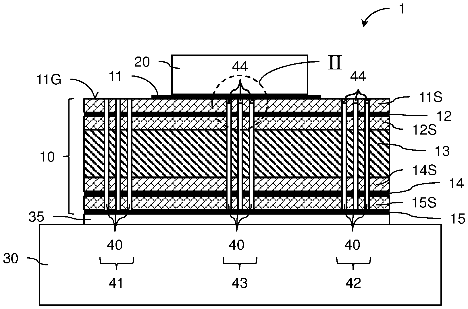
Die Erfindung betrifft ein elektronisches Modul mit verringerter elektromagnetischer Störabstrahlung. Dieses umfasst eine mehrlagige Leiterplatte (10) mit einer elektrisch leitenden Außenlage (11) und zumindest einer elektrisch leitenden Innenlage (12), ein elektronisches Bauelement (20), eine Wärmesenke (30) und eine Anzahl an thermischen Durchkontaktierungen (40). Das elektronische Bauelement (20) ist auf der Außenlage (11) angeordnet und elektrisch mit dieser verbunden. Die Wärmesenke (30) ist an die mehrlagige Leiterplatte (10) über eine elektrische Isolationsschicht (35) thermisch angebunden. Über die Anzahl an thermischen Durchkontaktierungen (40) kann im Betrieb des elektronischen Bauelements (20) erzeugte Wärme an die Wärmesenke (30) abgeführt werden. Die Anzahl an thermischen Durchkontaktierungen (40) weist keine elektrische Verbindung zu der Außenlage (11) auf.
Description
Die Erfindung betrifft ein elektronisches Modul mit einer mehrlagigen Leiterplatte, einem elektronischen Bauelement und einer Wärmesenke.The invention relates to an electronic module with a multilayer printed circuit board, an electronic component and a heat sink.
Bei elektronischen Modulen besteht das Problem, die im Betrieb eines elektronischen Bauelements anfallende Wärme durch die Leiterplatte hindurch an eine Wärmesenke abgeben zu können. Die Wärmesenke besteht zwecks guter Wärmeabfuhr in der Regel aus einem Metall. Zur Wärmeleitung werden in der Leiterplatte, die einen thermischen Widerstand darstellt, thermische Durchkontaktierungen (engl. : Vias) vorgesehen, die sich unterhalb des zu kühlenden elektronischen Bauelements von diesem in Richtung der Wärmesenke erstrecken. Thermische Durchkontaktierungen sind durch die Leiterplatte hindurchgehende und mit wärmeleitendem Material, in der Regel Kupfer, ausgefüllte Bohrungen. Die thermischen Durchkontaktierungen tragen in der Regel nicht zur Signalführung bei, sondern dienen ausschließlich der Wärmeleitung. Um eine elektrische Isolation zwischen der Wärmesenke und der Leiterplatte sicherzustellen, ist zwischen der Wärmesenke und der Leiterplatte eine elektrische Isolationsschicht vorgesehen. Zur Erzielung eines möglichst geringen Wärmewiderstands wird diese elektrische Isolationsschicht sehr dünn ausgeführt.In the case of electronic modules, there is the problem of being able to deliver the heat arising during operation of an electronic component through the printed circuit board to a heat sink. The heat sink is for the purpose of good heat dissipation usually made of a metal. For thermal conduction, thermal vias are provided in the printed circuit board, which represents a thermal resistance, which extend below the electronic component to be cooled from the latter in the direction of the heat sink. Thermal vias are through the PCB passing and with heat conductive material, usually copper, filled holes. The thermal vias do not usually contribute to the signal routing, but are used exclusively for heat conduction. To ensure electrical insulation between the heat sink and the circuit board, an electrical insulation layer is provided between the heat sink and the circuit board. To achieve the lowest possible thermal resistance, this electrical insulation layer is made very thin.
Die elektrische Isolationsschicht stellt eine (parasitäre) kleine elektrische Kapazität dar, deren Größe von der Dicke, Größe der Fläche und dem verwendeten Material abhängt. Über diese parasitäre Kapazität kann höher-frequente elektromagnetische Strahlung auf die Wärmesenke (z.B. ein metallisches Gehäuse, in dem das elektronische Modul angeordnet ist) übertragen und von dort abgestrahlt werden. Die Höhe bzw. Intensität der elektromagnetischen Strahlung ist abhängig von der Qualität bzw. Zuverlässigkeit der Erdung des metallischen Gehäuses, z.B. in einem Fahrzeug.The electrical insulation layer represents a (parasitic) small electrical capacitance, the size of which depends on the thickness, size of the area and the material used. By way of this parasitic capacitance, higher frequency electromagnetic radiation can be transmitted to and radiated from the heat sink (e.g., a metallic housing in which the electronic module is disposed). The intensity of the electromagnetic radiation depends on the quality or reliability of the grounding of the metallic housing, e.g. in a vehicle.
Es wäre wünschenswert, die Erzeugung elektromagnetischer Abstrahlung bereits aufgrund der Konstruktion des elektronischen Moduls unterdrücken oder verringern zu können, unabhängig von der Qualität der späteren elektrischen Anbindung des elektronischen Moduls in einem metallischen Gehäuse und/oder dem Verbau des elektronischen Moduls bei einem Kunden.It would be desirable to be able to suppress or reduce the generation of electromagnetic radiation already due to the construction of the electronic module, regardless of the quality of the subsequent electrical connection of the electronic module in a metallic housing and / or the installation of the electronic module at a customer.
Es ist Aufgabe der vorliegenden Erfindung, ein elektronisches Modul anzugeben, das funktionell und/oder baulich derart verbessert ist, dass die Gefahr elektromagnetischer Störabstrahlung verringert oder eliminiert ist.It is an object of the present invention to provide an electronic module that is functionally and / or structurally improved in such a way that the risk of electromagnetic interference radiation is reduced or eliminated.
Diese Aufgabe wird gelöst durch ein elektronisches Modul gemäß den Merkmalen des Anspruchs 1. Vorteilhafte Ausgestaltungen ergeben sich aus den abhängigen Patentansprüchen.This object is achieved by an electronic module according to the features of
Zur Lösung dieser Aufgabe wird ein elektronisches Modul vorgeschlagen, das eine mehrlagige Leiterplatte, ein elektronisches Bauelement, eine Wärmesenke und eine Anzahl an thermischen Durchkontaktierungen umfasst. Die mehrlagige Leiterplatte umfasst eine elektrisch leitende Außenlage und zumindest eine elektrisch leitende Innenlage. Das elektronische Bauelement ist auf der Außenlage angeordnet und elektrisch mit dieser verbunden. Die Wärmesenke ist an die mehrlagige Leiterplatte über eine elektrische Isolationsschicht thermisch angebunden. Über die Anzahl an thermischen Durchkontaktierungen kann die im Betrieb des elektronischen Bauelements erzeugte Wärme an die Wärmesenke abgeführt werden. Dabei weist die Anzahl an thermischen Durchkontaktierungen keine elektrische Verbindung zu der Außenlage auf.To solve this problem, an electronic module is proposed, which comprises a multilayer printed circuit board, an electronic component, a heat sink and a number of thermal vias. The multilayer printed circuit board comprises an electrically conductive outer layer and at least one electrically conductive inner layer. The electronic component is arranged on the outer layer and electrically connected thereto. The heat sink is thermally connected to the multilayer printed circuit board via an electrical insulation layer. Through the number of thermal vias, the heat generated during operation of the electronic component can be dissipated to the heat sink. In this case, the number of thermal vias has no electrical connection to the outer layer.
Bei dem erfindungsgemäßen elektronischen Modul erfolgt an einer Oberseite der mehrlagigen Leiterplatte eine elektrische Trennung zwischen der elektrisch leitenden Außenlage, auf der das elektronische Bauelement angeordnet ist, und den thermischen Durchkontaktierungen. Hierdurch kann elektromagnetische Störabstrahlung über die Wärmesenke oder ein metallisches Gehäuse, mit dem das elektronische Modul verbunden ist, verringert oder vermieden werden.In the case of the electronic module according to the invention, an electrical separation takes place on an upper side of the multilayer printed circuit board between the electrically conductive outer layer, on which the electronic component is arranged, and the thermal vias. As a result, electromagnetic interference radiation via the heat sink or a metallic housing, with which the electronic module is connected, can be reduced or avoided.
Es ist zweckmäßig, wenn die Anzahl an thermischen Durchkontaktierungen eine erste Gruppe an Durchkontaktierungen umfasst, welche in einer Schnittansicht außerhalb einer Fläche der Außenlage angeordnet ist. Insbesondere kann die Anzahl an Durchkontaktierungen der ersten Gruppe an Durchkontaktierungen bis zu einer Grenzfläche einer Isolationsschicht reichen, auf der die Außenlage angeordnet ist. Mit anderen Worten wird die Außenlage der mehrlagigen Leiterplatte nicht über die gesamte Fläche der Leiterplatte ausgebildet, sondern spart zumindest den Bereich der Leiterplatte, in dem die erste Gruppe an Durchkontaktierungen vorgesehen ist, aus. Die derart „strukturierte“ Außenlage kann im Rahmen der Herstellung der Leiterplatte durch ein subtraktives oder ein additives Verfahren erfolgen.It is expedient if the number of thermal plated-through holes comprises a first group of plated-through holes, which is arranged in a sectional view outside a surface of the outer layer. In particular, the number of plated-through holes of the first group of plated-through holes can reach up to an interface of an insulating layer on which the outer layer is arranged. In other words, the outer layer of the multilayer printed circuit board is not formed over the entire surface of the printed circuit board, but at least saves the area of the printed circuit board in which the first group of plated-through holes is provided. The so "structured" outer layer can be done in the context of manufacturing the circuit board by a subtractive or an additive method.
Gemäß einer anderen Ausgestaltung umfasst die Anzahl an thermischen Durchkontaktierungen eine zweite Gruppe an Durchkontaktierungen, welche in einer Schnittansicht unterhalb der Außenlage angeordnet ist. Bei dieser Ausgestaltung kann vorgesehen sein, dass die Außenlage im Bereich der thermischen Durchkontaktierungen der zweiten Gruppe an Durchkontaktierungen eine Aussparung aufweist. Dadurch wird ein elektrischer Kontakt zwischen der Außenlage und den Durchkontaktierungen der zweiten Gruppe an Durchkontaktierungen vermieden. Die Aussparung der Außenlage kann im Rahmen der Herstellung der Leiterplatte durch ein additives oder subtraktives Verfahren erzeugt werden.According to another embodiment, the number of thermal vias comprises a second group of vias, which is arranged in a sectional view below the outer layer. In this embodiment, it can be provided that the outer layer has a recess in the region of the thermal plated-through holes of the second group of plated-through holes. As a result, an electrical contact between the outer layer and the plated-through holes of the second group of plated-through holes avoided. The recess of the outer layer can be generated during the production of the printed circuit board by an additive or subtractive method.
Es kann weiterhin vorgesehen sein, wenn die freien Enden der Anzahl an Durchkontaktierungen der ersten Gruppe an Durchkontaktierungen und/oder die Anzahl an Durchkontaktierungen der zweiten Gruppe an Durchkontaktierungen auf oder unterhalb der Grenzfläche der Isolationsschicht, auf der die Außenlage angeordnet ist, mit einem Isolationsmaterial, insbesondere einem Lötstopplack, bedeckt sind. Hierdurch ist sichergestellt, dass kein elektrischer Kontakt zwischen der Außenlage und den thermischen Durchkontaktierungen besteht, wenn die Außenlage über die Durchkontaktierungen der zweiten Gruppe an Durchkontaktierungen hinweg führt, also in diesem Bereich keine Aussparung aufweist. Durch die Vermeidung eines elektrischen Kontakts zwischen der Außenlage und den Durchkontaktierungen der zweiten Gruppe an Durchkontaktierungen elektromagnetische Störstrahlung reduziert oder vermieden werden.It can furthermore be provided if the free ends of the number of plated-through holes of the first group of plated-through holes and / or the number of plated-through holes of the second group of plated-through holes on or below the boundary surface of the insulating layer on which the outer layer is arranged, with an insulating material, especially a solder mask, are covered. This ensures that there is no electrical contact between the outer layer and the thermal plated-through holes when the outer layer leads through the plated-through holes of the second group of plated-through holes, that is to say in this region there is no cutout. By avoiding an electrical contact between the outer layer and the plated-through holes of the second group of plated-through holes, electromagnetic interference radiation can be reduced or avoided.
Eine weitere zweckmäßige Ausgestaltung sieht vor, dass zumindest ein Teil der Anzahl an thermischen Durchkontaktierungen elektrisch mit der zumindest einen Innenlage und/oder einer weiteren Außenlage verbunden ist, welche jeweils ein Bezugspotential aufweisen. Dadurch, dass die thermischen Durchkontaktierungen, welche ausschließlich der Wärmeübertragung dienen, mit einem Bezugspotential (z.B. einem Massepotential) verbunden sind, können höher-frequente Störstrahlungen aufgrund eines kapazitiven Übergangs der Außenlage zur ersten Innenlage stark gedämpft werden. Ferner ist eine gute Wärmeverteilung über die Breite der Leiterplatte sichergestellt.A further expedient embodiment provides that at least part of the number of thermal plated-through holes is electrically connected to the at least one inner layer and / or a further outer layer, which each have a reference potential. By connecting the thermal vias serving exclusively for heat transfer to a reference potential (e.g., a ground potential), higher-frequency spurious radiations due to a capacitive transition of the outer layer to the first inner layer can be strongly attenuated. Furthermore, a good heat distribution over the width of the circuit board is ensured.
Es ist weiterhin zweckmäßig, wenn zumindest ein Teil der Anzahl an thermischen Durchkontaktierungen elektrisch zumindest mit der Innenlage verbunden ist, welche der Außenlage als nächstes benachbart ist. Hierdurch ist eine gute Wärmeverteilung über die Breite der Leiterplatte mittels der elektrisch und damit thermisch miteinander verbundenen thermischen Durchkontaktierungen gewährleistet. Insbesondere kann dadurch die Verteilung der Wärme bereits unmittelbar unterhalb des elektronischen Bauelements bewirkt werden, wobei am Wärmetransfer jedoch nicht die Außenlage, sondern als erstes diejenige Innenlage beteiligt ist, welche der Außenlage als nächstes benachbart ist.It is also expedient if at least part of the number of thermal plated-through holes is electrically connected at least to the inner layer which is adjacent to the outer layer next. As a result, a good heat distribution over the width of the circuit board is ensured by means of electrically and thus thermally interconnected thermal vias. In particular, the distribution of the heat can thus already be effected directly below the electronic component, wherein, however, the heat transfer does not involve the outer layer, but rather the inner layer which is adjacent to the outer layer as the first.
Der Erfindung liegt zusammenfassend die Überlegung zugrunde, dass zwei elektrisch isolierte Lagen einer Leiterplatte zueinander eine elektrische Kapazität darstellen. Hochfrequente Schwingungen können deshalb kapazitiv von einer elektrisch isolierten Lage auf eine andere elektrisch leitende Lage übertragen werden. Bekannte Lösungen versuchen, den kapazitiven Wert der elektrischen Isolationsschicht sehr klein zu halten, um die kapazitive Übertragung auf die Wärmesenke zu verringern. Dies führt jedoch meist zu einer Verschlechterung des Wärmeübergangs von der elektrischen Isolationsschicht zu der Wärmesenke. Die kapazitive Übertragung von hochfrequenten Schwingungen zwischen der Außenlage zu der Innenlage kann stark gedämpft werden, indem mindestens eine der Lagen, die mit den thermischen Durchkontaktierungen elektrisch verbunden sind, mit Bezugspotential, z.B. Masse, verbunden werden. Dadurch wird die Übertragung der hochfrequenten Schwingung zum Gehäuse quasi kurzgeschlossen. In der vorgeschlagenen Anordnung kann der Wärmeübergang von der elektrischen Isolationsschicht zu der Wärmesenke daher optimiert werden.The invention is based in summary on the consideration that two electrically insulated layers of a printed circuit board to each other represent an electrical capacitance. High-frequency oscillations can therefore be transmitted capacitively from one electrically insulated layer to another electrically conductive layer. Known solutions attempt to keep the capacitive value of the electrical insulation layer very small in order to reduce the capacitive transfer to the heat sink. However, this usually leads to a deterioration of the heat transfer from the electrical insulation layer to the heat sink. The capacitive transmission of high frequency oscillations between the outer layer and the inner layer can be greatly attenuated by applying at least one of the layers electrically connected to the thermal vias to reference potential, e.g. Mass, be connected. As a result, the transmission of the high-frequency oscillation to the housing is virtually short-circuited. In the proposed arrangement, the heat transfer from the electrical insulation layer to the heat sink can therefore be optimized.
Die Erfindung wird nachfolgend näher anhand eines Ausführungsbeispiels in der Zeichnung beschrieben. Es zeigen:
-
1 eine schematische Querschnittsdarstellung eines erfindungsgemäßen elektronischen Moduls; und -
2 eine vergrößerte Ansicht des in1 mit II gekennzeichneten Bereichs.
-
1 a schematic cross-sectional view of an electronic module according to the invention; and -
2 an enlarged view of the in1 Area marked II.
Die Leiterplatte
Auf einer Fläche der Außenlage
Die Leiterplatte
Die im Betrieb des elektronischen Bauelements
Die Anzahl an thermischen Durchkontaktierungen
Die Durchkontaktierungen
Demgegenüber sind die freien Enden der Durchkontaktierungen
Dieser Sachverhalt ist vergrößert in
Die Durchkontaktierungen
Durch die elektrische Verbindung zumindest einer Innenlage
Für den Fachmann ist klar, dass unter der Bezeichnung „die Innenlage
Bei dem vorgeschlagenen elektronischen Modul weist die Außenlage
Eine Reduktion des thermischen Widerstands kann, wie beschrieben, dadurch realisiert werden, dass die Durchkontaktierungen
Grundsätzlich kann das elektronische Modul
Dadurch, dass eine elektrische Isolationsschicht an der Seite der Leiterplatte
Die beschriebene Umsetzung verbessert zusätzlich die ESD-Empfindlichkeit. Bei einer Endladung eines ESD-Pulses auf das die Wärmesenke darstellende Metallgehäuse wird die hohe Spitzen-Spannung (Energie) durch die doppelte Barriere (isolierter Übergang vom Metallgehäuse zur Leiterplatte und isolierter Übergang von der Leiterplatte zu dem oder den Bauelementen) stark reduziert und somit eine Gefährdung bzw. Schädigung des oder der Bauelemente vermieden.The described implementation additionally improves the ESD sensitivity. At a final charge of an ESD pulse to the heat sink representing metal housing, the high peak voltage (energy) is greatly reduced by the double barrier (isolated transition from the metal housing to the circuit board and isolated transition from the circuit board to the one or more components) and thus a Danger or damage to the component (s) avoided.
Claims (8)
Priority Applications (3)
| Application Number | Priority Date | Filing Date | Title |
|---|---|---|---|
| DE102017220417.6A DE102017220417A1 (en) | 2017-11-16 | 2017-11-16 | Electronic module |
| CN201811366309.7A CN109803483B (en) | 2017-11-16 | 2018-11-16 | electronic module |
| US16/193,067 US10631399B2 (en) | 2017-11-16 | 2018-11-16 | Electronic module |
Applications Claiming Priority (1)
| Application Number | Priority Date | Filing Date | Title |
|---|---|---|---|
| DE102017220417.6A DE102017220417A1 (en) | 2017-11-16 | 2017-11-16 | Electronic module |
Publications (1)
| Publication Number | Publication Date |
|---|---|
| DE102017220417A1 true DE102017220417A1 (en) | 2019-05-16 |
Family
ID=66335440
Family Applications (1)
| Application Number | Title | Priority Date | Filing Date |
|---|---|---|---|
| DE102017220417.6A Withdrawn DE102017220417A1 (en) | 2017-11-16 | 2017-11-16 | Electronic module |
Country Status (3)
| Country | Link |
|---|---|
| US (1) | US10631399B2 (en) |
| CN (1) | CN109803483B (en) |
| DE (1) | DE102017220417A1 (en) |
Cited By (1)
| Publication number | Priority date | Publication date | Assignee | Title |
|---|---|---|---|---|
| DE102024208680A1 (en) * | 2024-09-12 | 2026-03-12 | Zf Friedrichshafen Ag | Electronic circuit and method for manufacturing an electronic circuit |
Families Citing this family (5)
| Publication number | Priority date | Publication date | Assignee | Title |
|---|---|---|---|---|
| CN108684134B (en) * | 2018-05-10 | 2020-04-24 | 京东方科技集团股份有限公司 | Circuit board and display device |
| DE102020203145B4 (en) * | 2020-03-11 | 2023-02-09 | Vitesco Technologies GmbH | circuit board arrangement |
| DE102020128729B4 (en) * | 2020-11-02 | 2025-09-18 | Audi Aktiengesellschaft | Arrangement for exchanging heat |
| TWI818870B (en) * | 2023-02-17 | 2023-10-11 | 華碩電腦股份有限公司 | Heat isolation pad and electronic device having the same |
| JP2024135584A (en) * | 2023-03-23 | 2024-10-04 | 株式会社東芝 | Storage |
Family Cites Families (17)
| Publication number | Priority date | Publication date | Assignee | Title |
|---|---|---|---|---|
| US6559525B2 (en) * | 2000-01-13 | 2003-05-06 | Siliconware Precision Industries Co., Ltd. | Semiconductor package having heat sink at the outer surface |
| US7202419B2 (en) * | 2004-07-20 | 2007-04-10 | Dragonwave Inc. | Multi-layer integrated RF/IF circuit board including a central non-conductive layer |
| US7196274B2 (en) * | 2004-07-20 | 2007-03-27 | Dragonwave Inc. | Multi-layer integrated RF/IF circuit board |
| TWI245388B (en) * | 2005-01-06 | 2005-12-11 | Phoenix Prec Technology Corp | Three dimensional package structure of semiconductor chip embedded in substrate and method for fabricating the same |
| JP2007188916A (en) * | 2006-01-11 | 2007-07-26 | Renesas Technology Corp | Semiconductor device |
| JP4962228B2 (en) * | 2006-12-26 | 2012-06-27 | 株式会社ジェイテクト | Multi-layer circuit board and motor drive circuit board |
| WO2009002381A2 (en) * | 2007-06-22 | 2008-12-31 | Skyworks Solutions, Inc. | Mold compound circuit structure for enhanced electrical and thermal performance |
| US7808788B2 (en) * | 2007-06-29 | 2010-10-05 | Delphi Technologies, Inc. | Multi-layer electrically isolated thermal conduction structure for a circuit board assembly |
| US8841171B2 (en) * | 2010-11-22 | 2014-09-23 | Bridge Semiconductor Corporation | Method of making stackable semiconductor assembly with bump/flange heat spreader and dual build-up circuitry |
| US20120126399A1 (en) * | 2010-11-22 | 2012-05-24 | Bridge Semiconductor Corporation | Thermally enhanced semiconductor assembly with bump/base/flange heat spreader and build-up circuitry |
| CN103384442A (en) * | 2013-03-13 | 2013-11-06 | 陈夏新 | Heat conducting structure with electronic power element adhered on circuit board |
| US9668352B2 (en) * | 2013-03-15 | 2017-05-30 | Sumitomo Electric Printed Circuits, Inc. | Method of embedding a pre-assembled unit including a device into a flexible printed circuit and corresponding assembly |
| SG10201400390YA (en) * | 2014-03-05 | 2015-10-29 | Delta Electronics Int L Singapore Pte Ltd | Package structure |
| SG10201400396WA (en) * | 2014-03-05 | 2015-10-29 | Delta Electronics Int’L Singapore Pte Ltd | Package structure and stacked package module with the same |
| US9332632B2 (en) * | 2014-08-20 | 2016-05-03 | Stablcor Technology, Inc. | Graphene-based thermal management cores and systems and methods for constructing printed wiring boards |
| TWM507138U (en) * | 2015-03-25 | 2015-08-11 | Polytronics Technology Corp | Thermal circuit board |
| US10182494B1 (en) * | 2017-09-07 | 2019-01-15 | Flex Ltd. | Landless via concept |
-
2017
- 2017-11-16 DE DE102017220417.6A patent/DE102017220417A1/en not_active Withdrawn
-
2018
- 2018-11-16 CN CN201811366309.7A patent/CN109803483B/en active Active
- 2018-11-16 US US16/193,067 patent/US10631399B2/en active Active
Cited By (1)
| Publication number | Priority date | Publication date | Assignee | Title |
|---|---|---|---|---|
| DE102024208680A1 (en) * | 2024-09-12 | 2026-03-12 | Zf Friedrichshafen Ag | Electronic circuit and method for manufacturing an electronic circuit |
Also Published As
| Publication number | Publication date |
|---|---|
| CN109803483B (en) | 2022-05-10 |
| CN109803483A (en) | 2019-05-24 |
| US10631399B2 (en) | 2020-04-21 |
| US20190150272A1 (en) | 2019-05-16 |
Similar Documents
| Publication | Publication Date | Title |
|---|---|---|
| DE102017220417A1 (en) | Electronic module | |
| EP0590354B1 (en) | Device with a board, a heat sink and at least one power component | |
| DE19911731C2 (en) | Printed circuit board | |
| DE102015108911B4 (en) | planar transformer for energy transmission | |
| EP2724597A2 (en) | Electronic assembly and method for the production thereof | |
| DE102015226712B4 (en) | PRINTED CIRCUIT BOARD AND ELECTRONIC COMPONENT | |
| DE102021000469A1 (en) | electronic device | |
| DE102017207727B4 (en) | semiconductor device | |
| DE102022130260A1 (en) | electrical module | |
| DE102011088256A1 (en) | Multilayer printed circuit board and arrangement with such | |
| DE102022109792B4 (en) | Power semiconductor module | |
| DE202014006215U1 (en) | Printed circuit board with cooled component, in particular SMD component | |
| WO2022263543A1 (en) | Circuit board assembly | |
| DE102014202196B3 (en) | Printed circuit board and circuit arrangement | |
| DE102021004458A1 (en) | Circuit board and circuit arrangement | |
| DE102008026347B4 (en) | Power electronic device with a substrate and a base body | |
| DE102015006456A1 (en) | PCB integrated power electronics | |
| DE102018007042B4 (en) | Power electronics | |
| DE102022119084A1 (en) | PCB assembly | |
| DE102016211968A1 (en) | Electronic component and method for manufacturing an electronic component | |
| DE102023110306A1 (en) | POWER MODULE | |
| DE102020100742B4 (en) | light module, lighting device and motor vehicle | |
| DE102018217607A1 (en) | Semiconductor component arrangement, method for their production and heat dissipation device | |
| DE102024205526B3 (en) | Circuit arrangement | |
| DE102024000910A1 (en) | Printed circuit board-heat sink assembly and method for producing a printed circuit board-heat sink assembly |
Legal Events
| Date | Code | Title | Description |
|---|---|---|---|
| R012 | Request for examination validly filed | ||
| R081 | Change of applicant/patentee |
Owner name: VITESCO TECHNOLOGIES GMBH, DE Free format text: FORMER OWNER: CONTINENTAL AUTOMOTIVE GMBH, 30165 HANNOVER, DE |
|
| R081 | Change of applicant/patentee |
Owner name: VITESCO TECHNOLOGIES GMBH, DE Free format text: FORMER OWNER: VITESCO TECHNOLOGIES GMBH, 30165 HANNOVER, DE |
|
| R120 | Application withdrawn or ip right abandoned |