Ausführungsformen der vorliegenden Erfindung betreffen eine elektronische Schaltung, insbesondere eine elektronische Treiberschaltung zum Ansteuern kapazitiver Lasten, wie beispielsweise das Gate eines Transistors.Embodiments of the present invention relate to an electronic circuit, in particular an electronic driver circuit for driving capacitive loads, such as the gate of a transistor.
MOS-Transistoren, wie beispielsweise MOSFETs (Metal Oxide Semiconductor Field-Effect Transistors) oder IGBTs (Insulated Gate Bipolar Transistors), werden häufig in Kfz-Applikationen, industriellen Applikationen oder Applikationen im Bereich der Unterhaltungselektronik zum Ansteuern von Lasten, zur Leistungswandlung, oder ähnlichem verwendet. MOS-Transistoren sind spannungsgesteuerte Bauteile, welche eine interne Kapazität aufweisen (oft auch als Gate-Source-Kapazität bezeichnet), welche durch eine Gate-Elektrode, ein Gate-Dielektrikum, sowie Body- und Source-Gebiete gebildet wird. Der MOS-Transistor kann ein- und ausgeschaltet werden, indem die interne Kapazität geladen oder entladen wird, wobei das Einschalten entweder das Laden oder das Entladen der internen Kapazität und das Ausschalten das entsprechend entgegengesetzte (Laden oder Entladen) der internen Kapazität aufweist. In einem MOS-Transistor vom Anreicherungstyp, beispielsweise, weist das Einschalten des MOS-Transistors das Laden der internen Kapazität und das Ausschalten des MOS-Transistors das Entladen der internen Kapazität auf. Es ist wünschenswert, diese MOS-Transistoren mit einer hohen Frequenz zu schalten, das heißt die interne Kapazität mit einer hohen Rate zu laden und entladen.MOS transistors, such as MOSFETs (Metal Oxide Semiconductor Field-Effect Transistors) or IGBTs (Insulated Gate Bipolar Transistors), are often used in automotive applications, industrial applications or applications in the field of entertainment electronics for controlling loads, for power conversion, or the like used. MOS transistors are voltage-controlled components which have an internal capacitance (often also referred to as gate-source capacitance), which is formed by a gate electrode, a gate dielectric, and body and source regions. The MOS transistor can be turned on and off by charging or discharging the internal capacitance, with turning on having either charging or discharging of the internal capacitance and turning off having the corresponding opposite (charging or discharging) of the internal capacitance. In an enhancement type MOS transistor, for example, turning on the MOS transistor includes charging the internal capacitance, and turning off the MOS transistor includes discharging the internal capacitance. It is desirable to switch these MOS transistors at a high frequency, that is, to charge and discharge the internal capacitance at a high rate.
In TIETZE, U.; SCHENK, CH.: Halbleiter-Schaltungstechnik, 11. Auflage, Berlin Heidelberg New York: Springer, 1999 - ISBN 3-540-64192-0, Seite 961 ist ein linearer Spannungsregler beschrieben, der einen Emitterfolger aufweist.In TIETZE, U .; SCHENK, CH .: Semiconductor circuit technology, 11 . Edition, Berlin Heidelberg New York: Springer, 1999 - ISBN 3-540-64192-0, page 961 describes a linear voltage regulator which has an emitter follower.
Die DE 101 27 868 A1 zeigt in 4 eine Halbbrückenschaltung mit einem High-Side-Transistor und einem Low-Side-Transistor, die jeweils als IGBT ausgebildet sind. Zur Spannungsversorgung einer Treiberschaltung des High-Side-Schalters ist eine Bootstrapschaltung mit einer Diode und einem Bootstrap-Kondensator, ein weiterer Kondensator und ein Strombegrenzer vorgesehen. Der weitere Kondensator ist zwischen Versorgungsanschlüsse der Treiberschaltung geschaltet und kann über den Strombegrenzer aus dem Bootstrap-Kondensator geladen werden.the DE 101 27 868 A1 shows in 4th a half-bridge circuit with a high-side transistor and a low-side transistor, each of which is designed as an IGBT. A bootstrap circuit with a diode and a bootstrap capacitor, a further capacitor and a current limiter are provided for supplying voltage to a driver circuit of the high-side switch. The further capacitor is connected between the supply connections of the driver circuit and can be charged from the bootstrap capacitor via the current limiter.
Die DE 11 2007 002 270 T5 beschreibt eine Halbbrückenschaltung mit einem High-Side-Transistor und einem Low-Side- Transistor, die jeweils als IGBT ausgebildet sind. Eine Treiberschaltung zur Ansteuerung des Low-Side- Transistors umfasst eine Halbbrücke mit zwei komplementären Bipolartransistoren, die gemeinsam angesteuert sind und von denen einer zwischen einen Gateknoten des Low-Side- Transistors und einen Knoten für ein positives elektrisches Potential und einer zwischen einen Gateknoten des Low-Side- Transistors und einen Knoten für ein negatives elektrisches Potential geschaltet ist.the DE 11 2007 002 270 T5 describes a half-bridge circuit with a high-side transistor and a low-side transistor, each of which is designed as an IGBT. A driver circuit for controlling the low-side transistor comprises a half-bridge with two complementary bipolar transistors which are controlled together and of which one between a gate node of the low-side transistor and a node for a positive electrical potential and one between a gate node of the low -Side- transistor and a node for a negative electrical potential is connected.
Die der Erfindung zugrundeliegende Aufgabe besteht darin, eine elektronische Treiberschaltung zur Verfügung zu stellen, die in der Lage ist, kapazitive Lasten mit einer hohen Frequenz ansteuern kann, und ein entsprechendes Verfahren zur Verfügung zu stellen. Diese Aufgabe wird durch eine Treiberschaltung nach Anspruch 1 und ein Verfahren nach Anspruch 10 gelöst.The object on which the invention is based is to provide an electronic driver circuit which is capable of driving capacitive loads at a high frequency, and to provide a corresponding method. This object is achieved by a driver circuit according to claim 1 and a method according to claim 10.
Eine Ausführungsform betrifft eine elektronische Schaltung. Die elektronische Schaltung weist einen Eingang, der dazu ausgebildet ist ein Eingangssignal zu empfangen, einen Ausgang, der dazu ausgebildet ist mit einer Last verbunden zu werden, einen Ausgangstransistor mit einer Laststrecke und einem Steuerknoten, wobei die Laststrecke zwischen den Ausgang und einen ersten Versorgungsknoten geschaltet ist, und einen Ansteuertransistor auf, welcher eine Laststrecke und einen Steuerknoten aufweist, wobei die Laststrecke mit dem Steuerknoten des Ausgangstransistors verbunden ist. Ein erster elektronischer Schalter ist in Serie mit der Laststrecke des Ansteuertransistors geschaltet. Eine Vorspannungsschaltung (engl. biasing circuit) mit einer internen Impedanz ist zwischen den Ansteuerknoten des Ansteuertransistors und den ersten Versorgungsknoten geschaltet. Die elektronische Schaltung weist weiterhin eine Steuerschaltung auf, die dazu ausgebildet ist, das Eingangssignal zu empfangen und den ersten elektronischen Schalter basierend auf dem Eingangssignal anzusteuern.One embodiment relates to an electronic circuit. The electronic circuit has an input that is designed to receive an input signal, an output that is designed to be connected to a load, an output transistor with a load path and a control node, the load path being connected between the output and a first supply node and a control transistor which has a load path and a control node, the load path being connected to the control node of the output transistor. A first electronic switch is connected in series with the load path of the control transistor. A biasing circuit with an internal impedance is connected between the drive node of the drive transistor and the first supply node. The electronic circuit furthermore has a control circuit which is designed to receive the input signal and to control the first electronic switch based on the input signal.
Eine weitere Ausführungsform betrifft ein Verfahren. Das Verfahren weist das Ansteuern eines ersten Ausgangstransistors, welcher mit einem Ausgang einer Treiberschaltung verbunden ist, mittels eines ersten Treibers basierend auf einem ersten Steuersignal, und das Steuern einer Spannung über die Laststrecke des ersten Ausgangstransistors mit einem Spannungsregler auf.Another embodiment relates to a method. The method includes controlling a first output transistor, which is connected to an output of a driver circuit, by means of a first driver based on a first control signal, and controlling a voltage across the load path of the first output transistor with a voltage regulator.
Beispiele werden im Folgenden unter Bezug auf die Figuren erläutert. Die Figuren dienen dazu, bestimmte Grundsätze darzustellen, so dass nur solche Aspekte dargestellt sind, welche für das Verständnis dieser Grundsätze erforderlich sind. Die Figuren sind nicht maßstabsgetreu. In den Figuren beziehen sich die selben Bezugszeichen auf gleiche Merkmale.
- 1 zeigt eine elektronische Treiberschaltung mit einem Ausgangstransistor und einem Spannungsregler, gemäß einer Ausführungsform;
- 2 welche die 2A-2B umfasst, zeigt Zeitdiagramme eines Ausgangsstromes der Treiberschaltung aus 1 und eine herkömmliche Treiberschaltung;
- 3 zeigt eine Ausführungsform eines Treibers des Ausgangstransistors;
- 4A-4B zeigen verschiedene Ausführungsformen einer Stromquelle in dem Treiber aus 3;
- 5 zeigt eine Ausführungsform zum Verändern eines Ausgangsstromes der Treiberschaltung, basierend auf Lastparametern;
- 6 zeigt eine Ausführungsform eines Treibers des Ausgangstransistors;
- 7 zeigt eine weitere Ausführungsform des Treibers des Ausgangstransistors;
- 8 zeigt eine Ausführungsform eines Verstärkers in dem Treiber aus 7;
- 9 zeigt eine Ausführungsform einer Stromquelle in dem Treiber in 8;
- 10 zeigt eine weitere Ausführungsform der Stromquelle in dem Treiber aus 8;
- 11A-11B zeigen Ausführungsformen von Stromquellen in der Stromquelle aus 10;
- 12 zeigt Zeitdiagramme, welche eine Methode zum Betreiben der elektronischen Treiberschaltung aus 1 darstellen;
- 13 zeigt eine elektronische Treiberschaltung mit einer High-Side-Treiberschaltung und einer Low-Side-Treiberschaltung;
- 14 zeigt eine Ausführungsform der Low-Side-Treiberschaltung in größerem Detail;
- 15 zeigt eine Ausführungsform eines Treibers in der Low-Side-Treiberschaltung aus 9;
- 16 zeigt eine weitere Ausführungsform eines Treibers in der Low-Side-Treiberschaltung aus 9; und
- 17 zeigt eine elektronische Treiberschaltung mit einer Klemmschaltung gemäß einer Ausführungsform.
Examples are explained below with reference to the figures. The figures serve to illustrate certain principles, so that only those aspects are shown which are necessary for an understanding of these principles. The figures are not true to scale. In the figures, the same reference symbols relate to the same features. - 1 shows an electronic driver circuit with an output transistor and a voltage regulator, according to an embodiment;
- 2 those who 2A-2B shows timing diagrams of an output current of the driver circuit 1 and a conventional driver circuit;
- 3 Figure 3 shows one embodiment of a driver of the output transistor;
- 4A-4B show various embodiments of a current source in the driver 3 ;
- 5 shows an embodiment for changing an output current of the driver circuit based on load parameters;
- 6th Figure 3 shows one embodiment of a driver of the output transistor;
- 7th shows another embodiment of the driver of the output transistor;
- 8th FIG. 14 shows one embodiment of an amplifier in the driver of FIG 7th ;
- 9 FIG. 11 shows one embodiment of a current source in the driver in FIG 8th ;
- 10 FIG. 8 shows another embodiment of the current source in the driver from FIG 8th ;
- 11A-11B show embodiments of power sources in the power source 10 ;
- 12th FIG. 10 shows timing diagrams showing a method of operating the electronic driver circuit 1 represent;
- 13th shows an electronic driver circuit with a high-side driver circuit and a low-side driver circuit;
- 14th Figure 3 shows one embodiment of the low-side driver circuit in greater detail;
- 15th FIG. 13 shows an embodiment of a driver in the low-side driver circuit from FIG 9 ;
- 16 FIG. 8 shows a further embodiment of a driver in the low-side driver circuit from FIG 9 ; and
- 17th shows an electronic driver circuit with a clamping circuit according to an embodiment.
In der folgenden detaillierten Beschreibung wird auf die beigefügten Figuren Bezug genommen. Die Figuren bilden einen Teil der Beschreibung und zeigen zur Veranschaulichung bestimmte Ausführungsformen, in welchen die Erfindung Verwendung finden kann. Es versteht sich, dass die Merkmale der beschriebenen Ausführungsformen miteinander kombiniert werden können, sofern nicht anders angegeben.In the following detailed description, reference is made to the accompanying figures. The figures form a part of the description and show, by way of illustration, certain embodiments in which the invention can be used. It goes without saying that the features of the described embodiments can be combined with one another, unless stated otherwise.
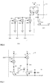
1 zeigt eine elektronische Treiberschaltung 100 gemäß einer Ausführungsform. Diese elektronische Treiberschaltung 100 ist dazu ausgebildet, eine Last anzusteuern, indem ein Ausgangstrom IOUT in die Last getrieben wird. Insbesondere ist die elektronische Treiberschaltung 100 dazu ausgebildet, eine kapazitive Last anzusteuern. Die kapazitive Last ist beispielsweise ein MOS-Transistor. Ein MOS-Transistor, wie beispielsweise ein MOSFET oder IGBT, ist ein spannungsgesteuertes Halbleiterbauelement, welches in Abhängigkeit eines Ladungszustandes einer internen Gate-Source-Kapazität ein- oder ausschaltet. Lediglich zum Zwecke der Illustration zeigt 1 eine kapazitive Last Z, welche als MOSFET implementiert ist, insbesondere als selbstsperrender n-Typ MOSFET. Dies ist jedoch lediglich ein Beispiel. Jegliche andere Art von MOS-Transistor kann ebenfalls von der elektronischen Treiberschaltung ansteuert werden. Die interne Gate-Source-Kapazität dieses MOSFETs wird durch einen Kondensator CGS repräsentiert, welche zwischen einen Gate-Knoten G und einen Source-Knoten S des MOSFETs Z geschaltet ist. 1 shows an electronic driver circuit 100 according to one embodiment. This electronic driver circuit 100 is designed to control a load by supplying an output current IOUT is driven into the load. In particular, the electronic driver circuit 100 designed to drive a capacitive load. The capacitive load is, for example, a MOS transistor. A MOS transistor, such as a MOSFET or IGBT, is a voltage-controlled semiconductor component which switches on or off depending on a state of charge of an internal gate-source capacitance. Shows for the purpose of illustration only 1 a capacitive load Z , which is implemented as a MOSFET, in particular as a normally-off n-type MOSFET. However, this is just an example. Any other type of MOS transistor can also be controlled by the electronic driver circuit. The internal gate-source capacitance of this MOSFET is provided by a capacitor CGS represents which between a gate node G and a source node S of the MOSFET Z is switched.
Bezugnehmend auf 1 weist die elektronische Treiberschaltung 100 einen Ausgang OUT auf, der dazu ausgebildet ist mit der Last Z verbunden zu werden und den Ausgangsstrom bereitzustellen. Für den Fall, dass die Last Z ein MOSFET ist (wie in 1 dargestellt) wird der Ausgang OUT der elektronischen Treiberschaltung 100 mit dem Gate-Knoten G des MOSFETs Z verbunden.Referring to 1 instructs the electronic driver circuit 100 an exit OUT on, which is designed to with the load Z to be connected and to provide the output current. In the event that the load Z is a MOSFET (as in 1 shown) is the output OUT the electronic driver circuit 100 with the gate node G of the MOSFET Z tied together.
Die elektronische Treiberschaltung 100 weist weiterhin einen Ausgangstransistor 11, einen Spannungsregler 3, 4 und einen Treiber 21 auf. Der Ausgangstransistor 11 weist einen Steuerknoten G11 und eine Laststrecke auf, welche zwischen den Ausgang OUT und einen ersten Versorgungsknoten 11 geschaltet ist. Der Spannungsregler 3, 4 ist dazu ausgebildet, eine Spannung VDS11 über der Laststrecke des Ausgangstransistors 11 zu steuern, und der Treiber 21 ist dazu ausgebildet, den Ausgangstransistor 11 basierend auf einem ersten Steuersignal CS11 anzusteuern. In der in 1 dargestellten Ausführungsform weist der Spannungsregler 3, 4 einen Regeltransistor 3 mit einem Steuerknoten G3 und einer Laststrecke auf. Die Laststrecke ist in Serie zu der Laststrecke des Ausgangstransistors 11 geschaltet, wobei eine Serienschaltung mit der Laststrecke des Regeltransistors 3 und der Laststrecke des Ausgangstransistors 11 zwischen den Ausgang OUT und einen ersten Versorgungsknoten 11 geschaltet ist. Der Spannungsregler 3, 4 weist weiterhin eine Vorspannungsquelle 4 (engl.: biasing voltage source) auf, welche zwischen den Steuerknoten G3 des Regeltransistors 3 und einen ersten Laststreckenknoten S11 des Ausgangstransistors geschaltet ist. In der in 1 dargestellten Ausführungsform ist der erste Laststreckenknoten S11 des Ausgangstransistors 11 mit dem Ausgang OUT verbunden.The electronic driver circuit 100 furthermore has an output transistor 11 , a voltage regulator 3 , 4th and a driver 21 on. The output transistor 11 has a control node G11 and a load path, which is between the output OUT and a first supply node 1 1 is switched. The voltage regulator 3 , 4th is designed to create a voltage VDS11 across the load path of the output transistor 11 to control, and the driver 21 is designed to use the output transistor 11 based on a first control signal CS11 head for. In the in 1 illustrated embodiment has the voltage regulator 3 , 4th a regulating transistor 3 with a control node G3 and a load path. The load path is in series with the load path of the output transistor 11 switched, with a series circuit with the load path of the control transistor 3 and the load path of the output transistor 11 between the exit OUT and a first supply node 1 1 is switched. The voltage regulator 3 , 4th further comprises a bias voltage source 4th (English: biasing voltage source), which between the control nodes G3 of the control transistor 3 and a first load route node S11 of the output transistor is switched. In the in 1 The embodiment shown is the first load route node S11 of the output transistor 11 with the exit OUT tied together.
Die oben beschriebenen Schaltelemente, das heißt der Ausgangstransistor 11, der Spannungsregler 3, 4 und der Treiber 21 sind Teil einer ersten Treiberschaltung 101, welche im Folgenden kurz als erster Treiber oder High-Side-Treiber bezeichnet wird. Dieser erste Treiber 101 ist dazu ausgebildet, eine kapazitive Last zu laden, welche mit dem Ausgang OUT verbunden ist. Wenn, wie in 1 dargestellt, die Last Z ein MOS-Transistor ist, welcher mit einem Gate-Knoten G mit dem Ausgang OUT verbunden ist, ist die kapazitive Last die interne Gate-Source-Kapazität CGS des MOS-Transistors. Das Aufladen dieser internen Gate-Source-Kapazität CGS mit dem ersten Treiber 101 entspricht dem Einschalten des MOS-Transistors Z. Neben dem ersten Treiber 101, der dazu ausgebildet ist, die kapazitive Last zu laden (einen MOS-Transistor einzuschalten) kann die elektronische Schaltung 100 einen zweiten Treiber aufweisen (in 1 nicht dargestellt), der dazu ausgebildet ist, die kapazitive Last zu entladen (den MOS-Transistor auszuschalten). Ein solcher zweiter Treiber wird im Weiteren noch beschrieben. Wenn die elektronische Schaltung 100 die kapazitive Last auflädt, fließt der Ausgangsstrom IOUT in eine in 1 dargestellte Richtung, und wenn die elektronische Schaltung 100 die kapazitive Last entlädt, fließt der Ausgangsstrom IOUT in eine der in 1 dargestellten entgegengesetzte Richtung.The switching elements described above, i.e. the output transistor 11 , the voltage regulator 3 , 4th and the driver 21 are part of a first driver circuit 101 , which is referred to below as the first driver or high-side driver. That first driver 101 is designed to charge a capacitive load, which is connected to the output OUT connected is. If, as in 1 shown, the load Z is a MOS transistor which has a gate node G with the exit OUT connected, the capacitive load is the internal gate-source capacitance CGS of the MOS transistor. The charging of this internal gate-source capacitance CGS with the first driver 101 corresponds to turning on the MOS transistor Z . Next to the first driver 101 , which is designed to charge the capacitive load (switch on a MOS transistor) can control the electronic circuit 100 have a second driver (in 1 not shown), which is designed to discharge the capacitive load (turn off the MOS transistor). Such a second driver is described below. When the electronic circuit 100 the capacitive load is charging, the output current flows IOUT into an in 1 direction shown and when the electronic circuit 100 the capacitive load discharges, the output current flows IOUT in one of the in 1 opposite direction shown.
Der erste Treiber 101 lädt die kapazitive Last CGS auf (schaltet den MOS-Transistor Z ein) wenn der Ausgangstransistor 11 in einem Ein-Zustand ist (eingeschaltet ist). Der Betriebszustand (ein oder aus) des Ausgangstransistors 11 wird durch den Treiber 21 basierend auf dem ersten Steuersignal CS11 geregelt. Das erste Steuersignal CS11 kann zwei verschiedene Signalpegel annehmen, nämlich einen Ein-Pegel und einen Aus-Pegel, wobei der Treiber 21 dazu ausgebildet sein kann, den Ausgangstransistor 11 einzuschalten, wenn das Steuersignal CS11 den Ein-Pegel annimmt und den Ausgangstransistor 11 auszuschalten, wenn das Steuersignal CS11 den Aus-Pegel annimmt.The first driver 101 charges the capacitive load CGS on (switches the MOS transistor Z a) if the output transistor 11 is in an on-state. The operating state (on or off) of the output transistor 11 is through the driver 21 based on the first control signal CS11 regulated. The first control signal CS11 can assume two different signal levels, namely an on-level and an off-level, whereby the driver 21 can be designed for this purpose, the output transistor 11 turn on when the control signal CS11 assumes the on-level and the output transistor 11 turn off when the control signal CS11 assumes the off level.
Eine Methode zum Betreiben des in 1 dargestellten ersten Treibers 101 wird im Folgenden beschrieben. Zum Zwecke der Erläuterung wird angenommen, dass der Ausgangstransistor 11 und der Regeltransistor 3 jeweils ein MOSFET vom n-Typ sind, insbesondere ein selbstsperrender n-Typ MOSFET. In diesem Fall ist der Steuerknoten des Ausgangstransistors 11 der Gate-Knoten des MOSFETS, welcher den Ausgangstransistor bildet, und der Steuerknoten des Regeltransistors 3 ist der Gate-Knoten des MOSFETs, welcher den Regeltransistor 3 bildet. Weiterhin sind die Laststrecken des Ausgangstransistors 11 und des Regeltransistors 3 jeweils die Drain-Source-Strecke des MOSFETs, welcher den entsprechenden Transistor 11, 3 bildet. Bezugnehmend auf 1 ist der Source-Knoten S11 des MOSFETs, welcher den Ausgangstransistor 11 bildet (im Folgenden kurz als der Source-Knoten des Ausgangstransistors 11 bezeichnet) mit dem Ausgang OUT verbunden, und der Drain-Knoten D11 ist mit dem Source-Knoten S3 des MOSFETs, welcher den Regeltransistor 3 bildet (im Folgenden kurz als der Source-Knoten S3 des Regeltransistors 3 bezeichnet) verbunden. Der Drain-Knoten D3 des Regeltransistors 3 ist mit dem ersten Versorgungsknoten 11 verbunden und der Gate-Knoten G3 des Regeltransistors 3 ist mit der Vorspannungsquelle 4 verbunden.One method of operating the in 1 shown first driver 101 is described below. For purposes of explanation it is assumed that the output transistor 11 and the regulating transistor 3 are each an n-type MOSFET, in particular a normally-off n-type MOSFET. In this case the control node is the output transistor 11 the gate node of the MOSFET, which forms the output transistor, and the control node of the regulating transistor 3 is the gate node of the MOSFET, which is the control transistor 3 forms. Furthermore, the load paths of the output transistor 11 and the control transistor 3 each the drain-source path of the MOSFET, which the corresponding transistor 11 , 3 forms. Referring to 1 is the source node S11 of the MOSFET, which is the output transistor 11 (hereinafter referred to as the source node of the output transistor for short 11 labeled) with the exit OUT connected, and the drain node D11 is with the source node S3 of the MOSFET, which is the control transistor 3 forms (hereinafter referred to as the source node for short S3 of the control transistor 3 designated) connected. The drain node D3 of the control transistor 3 is with the first supply node 1 1 connected and the gate node G3 of the control transistor 3 is with the bias source 4th tied together.
Der Ausgangstransistor 11 weist parasitäre Kapazitäten auf. Zwei dieser parasitären Kapazitäten sind in 1 dargestellt, nämlich eine Gate-Source-Kapazität CGS11 zwischen dem Gate-Knoten G11 und dem Source-Knoten S11 und eine Gate-Drain-Kapazität CGD11 zwischen dem Gate-Knoten G11 und dem Drain-Knoten D11. Der Ausgangstransistor 11 weist weiterhin eine Drain-Source-Kapazität zwischen dem Drain-Knoten D11 und dem Source-Knoten S11 auf. Diese Drain-Source-Kapazität ist jedoch in 1 nicht explizit dargestellt. Ebenso sind parasitäre Kapazitäten des Regeltransistors 3 in 1 nicht dargestellt. Der Ladungszustand der Gate-Source-Kapazität CGS11 des Ausgangstransistors 11 oder eine Gate-Source-Spannung VGS11 über der Gate-Source-Kapazität CGS11 definiert den Betriebszustand des Ausgangstransistors 11. Der Betriebszustand des Ausgangstransistors kann einen Ein-Zustand, in welchem der Ausgangstransistor eingeschaltet ist, und einen Aus-Zustand aufweisen, in welchem der Ausgangstransistor ausgeschaltet ist. Der Ausgangstransistor 11 befindet sich in dem Ein-Zustand, wenn die Gate-Source-Kapazität CGS11 durch den Treiber 21 derart geladen wurde, dass die Gate-Source-Spannung VGS11 eine Schwellenspannung des Ausgangstransistors 11 erreicht hat. Der Ausgangstransistor 11 befindet sich in dem Aus-Zustand, wenn die Gate-Source-Kapazität CGS11 durch den Treiber 21 derart entladen wurde, so dass die Gate-Source-Spannung VCS11 unterhalb einer Schwellenspannung des Ausgangstransistors 11 liegt. Der Regeltransistor 3 befindet sich in dem Aus-Zustand, wenn die Gate-Source-Spannung VGS3, also die Spannung zwischen dem Gate-Knoten G3 und dem Source-Knoten S3, unterhalb der Schwellenspannung des Regeltransistors 3 liegt, und der Regeltransistor 3 befindet sich in dem Ein-Zustand, wenn die Gate-Source-Spannung VGS3 oberhalb der Schwellenspannung des Regeltransistors 3 liegt. Beispielsweise kann die Schwellenspannung des Ausgangstransistors 11 und des Regeltransistors 3 jeweils mehrere Volt betragen. Gemäß einer weiteren Ausführungsform, welche im Folgenden noch beschrieben wird, weist der Ausgangstransistor 11 in dem Ein-Zustand verschiedene Betriebszustände bei verschiedenen Gate-Source-Spannungen VGS11 auf.The output transistor 11 exhibits parasitic capacitances. Two of these parasitic capacitances are in 1 shown, namely a gate-source capacitance CGS11 between the gate node G11 and the source node S11 and a gate-drain capacitance CGD11 between the gate node G11 and the drain node D11 . The output transistor 11 furthermore has a drain-source capacitance between the drain node D11 and the source node S11 on. However, this drain-source capacitance is in 1 not explicitly shown. There are also parasitic capacitances of the control transistor 3 in 1 not shown. The state of charge of the gate-source capacitance CGS11 of the output transistor 11 or a gate-source voltage VGS11 above the gate-source capacitance CGS11 defines the operating state of the output transistor 11 . The operating state of the output transistor can have an on state in which the output transistor is switched on and an off state in which the output transistor is switched off. The output transistor 11 is in the on-state when the gate-source capacitance CGS11 through the driver 21 was charged in such a way that the gate-source voltage VGS11 a threshold voltage of the output transistor 11 has reached. The output transistor 11 is in the off state when the gate-source capacitance CGS11 through the driver 21 was discharged so that the gate-source voltage VCS11 below a threshold voltage of the output transistor 11 lies. The control transistor 3 is in the off state when the gate-source voltage VGS3 , i.e. the voltage between the gate node G3 and the source node S3 , below the threshold voltage of the regulating transistor 3 lies, and the control transistor 3 is in the on-state when the gate-source voltage VGS3 above the threshold voltage of the control transistor 3 lies. For example, the threshold voltage of the output transistor 11 and the control transistor 3 each be several volts. According to In a further embodiment, which will be described below, the output transistor 11 in the on-state, different operating states at different gate-source voltages VGS11 on.
Wenn sich der Ausgangstransistor 11 in dem Aus-Zustand befindet, entspricht ein Spannungspegel der Drain-Source-Spannung VDS11, welche die Spannung zwischen dem Drain-Knoten D11 und dem Source-Knoten S11 ist, im Wesentlichen einem Spannungspegel der Vorspannung V4, welche durch die Vorspannungsquelle 4 bereitgestellt wird. In dem Ein-Zustand des Ausgangstransistors 11 treibt der Regeltransistor 3 einen Strom IDS11 durch den Ausgangstransistor 11, so dass die Drain-Source-Spannung VDS11 des Ausgangstransistors 11 im Wesentlichen konstant ist. Ein Pegel dieser Spannung VDS11 entspricht dem Pegel der Vorspannung V4 minus dem Pegel der Gate-Source-Spannung VGS3 des Regeltransistors 3. Da (wie in jedem MOSFET) der Strompegel des Stromes IDS11 durch den Regeltransistor 3 in dem Ein-Zustand des Regeltransistors 3 exponentiell von dem Pegel der Gate-Source-Spannung VGS3 abhängt, gibt es lediglich geringe Variationen der Gate-Source-Spannung VGS3, selbst wenn große Variationen des Stromes IDS11 auftreten können. Daher kann die Drain-Source-Spannung VDS11 des Ausgangstransistors 11 in dem Ein-Zustand des Regeltransistors 3 als im Wesentlichen konstant angenommen werden.When the output transistor 11 is in the off state, a voltage level corresponds to the drain-source voltage VDS11 showing the voltage between the drain node D11 and the source node S11 is, essentially a voltage level of the bias V4 , which by the bias source 4th provided. In the on-state of the output transistor 11 drives the control transistor 3 a stream IDS11 through the output transistor 11 so that the drain-source voltage VDS11 of the output transistor 11 is essentially constant. One level of that voltage VDS11 corresponds to the level of the bias V4 minus the level of the gate-source voltage VGS3 of the control transistor 3 . Since (as in every MOSFET) the current level of the current IDS11 through the control transistor 3 in the on-state of the regulating transistor 3 exponentially from the level of the gate-source voltage VGS3 there is little variation in gate-source voltage VGS3 even if there are large variations in the current IDS11 may occur. Therefore, the drain-source voltage VDS11 of the output transistor 11 in the on-state of the regulating transistor 3 can be assumed to be essentially constant.
Das Regeln des Pegels der Drain-Source-Spannung VDS11 des Ausgangstransistors 11 durch den Regeltransistor 3 hat den Effekt, dass keine wesentliche Abnahme des Drain-Source-Stromes IDS11 (der Ausgangsstrom IOUT) aufgrund des sogenannten Miller-Effekts auftritt. Hierin liegt der Unterschied zu herkömmlichen Treiberschaltungen, welche keinen Regeltransistor aufweisen, was im Folgenden beschrieben wird.Regulating the level of the drain-source voltage VDS11 of the output transistor 11 through the control transistor 3 has the effect that there is no significant decrease in the drain-source current IDS11 (the output current IOUT ) occurs due to the so-called Miller effect. This differs from conventional driver circuits which do not have a regulating transistor, which is described below.
Bevor der Ausgangstransistor 11 einschaltet, ist die Gate-Source-Spannung VGS11 im wesentlichen Null und der Pegel der Drain-Source-Spannung VDS11 entspricht im Wesentlichen dem Pegel der Vorspannung V4. Daher entspricht ein Pegel der Spannung zwischen dem Drain-Knoten D11 und dem Gate-Knoten G11 und über der Gate-Drain-Kapazität CGD11 im Wesentlichen dem Pegel der Vorspannung V4. Wenn der Treiber 21 basierend auf dem Steuersignal CS22 die Gate-Source-Kapazität CGS11 lädt, schaltet der Ausgangstransistor 11 ein, wenn der Pegel der Gate-Source-Spannung VGS11 über der Gate-Source-Kapazität CGS11 die Schwellenspannung erreicht.Before the output transistor 11 turns on is the gate-source voltage VGS11 substantially zero and the level of the drain-source voltage VDS11 corresponds essentially to the level of the bias voltage V4 . Therefore, one level corresponds to the voltage between the drain node D11 and the gate node G11 and across the gate-drain capacitance CGD11 essentially the level of the bias V4 . If the driver 21 based on the control signal CS22 the gate-source capacitance CGS11 loads, the output transistor switches 11 a when the level of the gate-source voltage VGS11 above the gate-source capacitance CGS11 reaches the threshold voltage.
Wird angenommen, dass der Regeltransistor 3 weggelassen wird, resultiert das Einschalten des Ausgangstransistors 11 in einer Verringerung der Drain-Source-Spannung VDS11. Da der Gate-Knoten G11 über die Gate-Drain-Kapazität CGD11 kapazitiv mit dem Drain-Knoten D11 verbunden ist, resultiert eine Verringerung der Drain-Source-Spannung VDS11 in einer Verringerung des elektrischen Potentials an dem Gate-Knoten G11 bis die Gate-Drain-Kapazität CGD11 entladen ist. Dies ist als Miller-Effekt bekannt und resultiert in einem Abfall des Stromes IDS11 durch den Ausgangstransistor 11. 2B zeigt ein Zeitdiagramm des Stromes IDS11 durch den Ausgangstransistor 11 in einer Treiberschaltung von dem in 1 dargestellten Typ, wenn der Regeltransistor 3 weggelassen wird.It is believed that the regulating transistor 3 is omitted, the output transistor turns on 11 in a decrease in drain-source voltage VDS11 . Because the gate node G11 via the gate-drain capacitance CGD11 capacitive with the drain node D11 is connected, a decrease in the drain-source voltage results VDS11 in a decrease in the electrical potential at the gate node G11 up the gate-drain capacitance CGD11 is discharged. This is known as the Miller effect and results in a drop in current IDS11 through the output transistor 11 . 2 B shows a timing diagram of the current IDS11 through the output transistor 11 in a driver circuit from the in 1 shown type if the regulating transistor 3 is omitted.
Der Regeltransistor 3 verhindert, dass sich die Drain-Source-Spannung VDS11 des Ausgangstransistors 11 signifikant verringert (abfällt), wenn der Ausgangstransistor 11 einschaltet. Daher wird der Miller-Effekt im Wesentlichen verhindert, so dass kein wesentlicher Abfall des Drain-Source-Stromes IDS11 (des Ausgangsstromes IOUT) durch den Ausgangstransistor 11 auftritt, nachdem der Ausgangstransistor 11 einschaltet. 2A zeigt ein Zeitdiagramm des Stromes IDS11 durch den Ausgangstransistor 11 in dem ersten Treiber 101 aus 1.The control transistor 3 prevents the drain-source voltage VDS11 of the output transistor 11 significantly decreases (drops) when the output transistor 11 turns on. The Miller effect is therefore essentially prevented, so that there is no substantial drop in the drain-source current IDS11 (of the output current IOUT ) through the output transistor 11 occurs after the output transistor 11 turns on. 2A shows a timing diagram of the current IDS11 through the output transistor 11 in the first driver 101 the end 1 .
3 zeigt eine Ausführungsform des Treibers 21, der den Ausgangstransistor 11 ansteuert. In dieser Ausführungsform weist der Treiber 21 einen Widerstand 211 auf, welcher in Serie zu einer Stromquelle 212 geschaltet ist. Der Widerstand 211 ist zwischen den Gate-Knoten G11 und den Source-Knoten S11 des Ausgangstransistors 11 geschaltet. Die Stromquelle 212 ist eine gesteuerte Stromquelle, welche durch ein erstes Steuersignal CS11 gesteuert wird. Die Stromquelle 212 ist zwischen den Widerstand 211 und einen zweiten Versorgungsknoten 12 geschaltet, an welchem ein Versorgungspotential V12 verfügbar ist. Dieses zweite Versorgungspotential V12 kann genauso groß sein, wie das erste Versorgungspotential V11 an dem ersten Versorgungsknoten 11 oder kann unterschiedlich zu dem ersten Versorgungspotential V11 sein. Gemäß einer Ausführungsform schaltet ein Ein-Pegel des Steuersignals CS11 die Stromquelle 212 ein, und ein Aus-Pegel des Steuersignals CS11 schaltet die Stromquelle 212 aus. Gemäß einer Ausführungsform ist ein Ausgangsstrom 1212 der Stromquelle 212 Null, wenn die Stromquelle 212 ausgeschaltet wurde und ein Strompegel des Ausgangsstroms 1212 unterscheidet sich von Null, wenn die Stromquelle 212 eingeschaltet wurde. Der Strompegel des Ausgangsstromes I212 in dem Ein-Zustand der Stromquelle 212 und ein Widerstandswert des Widerstands 211 bestimmen einen Betriebspunkt des Ausgangstransistors 11 in dem Ein-Zustand. Das heißt, dass der Pegel der Gate-Source-Spannung VGS11 des Ausgangstransistors 11 in dem stationären Zustand des Ausgangstransistors 11 im Wesentlichen gegeben ist durch:
wobei VGS11ON der Pegel der Gate-Source-Spannung VGS11 in dem Ein-Zustand des Ausgangstransistors, R211 der Widerstandswert des Widerstands 211 und I212ON der Strompegel des Stromes I212 in dem Ein-Zustand (aktivierter Zustand) der Stromquelle 212 ist. 3 Figure 3 shows one embodiment of the driver 21 that is the output transistor 11 drives. In this embodiment, the driver has 21 a resistance 211 on, which is in series with a power source 212 is switched. The resistance 211 is between the gate nodes G11 and the source node S11 of the output transistor 11 switched. The power source 212 is a controlled current source which is controlled by a first control signal CS11 is controlled. The power source 212 is between the resistance 211 and a second supply node 1 2 switched at which a supply potential V1 2 is available. This second supply potential V1 2 can be as large as the first supply potential V1 1 at the first supply node 1 1 or can be different from the first supply potential V1 1 be. According to one embodiment, an on-level of the control signal switches CS11 the power source 212 on, and an off level of the control signal CS11 switches the power source 212 the end. According to one embodiment, an output current is 1212 the power source 212 Zero if the power source 212 has been turned off and a current level of the output current 1212 differs from zero when the power source 212 has been switched on. The current level of the output current I212 in the on-state of the power source 212 and a resistance value of the resistor 211 determine an operating point of the output transistor 11 in the on-state. That is, the level of the gate-source voltage VGS11 of the output transistor 11 in the steady state of the output transistor 11 is essentially given by: where VGS11 ON is the level of the gate-source voltage VGS11 in the on-state of the output transistor, R211 the resistance value of the resistor 211 and I212 ON the current level of the current I212 in the on-state (activated state) of the power source 212 is.
4A zeigt eine Ausführungsform der steuerbaren Stromquelle 212. Diese Stromquelle 212 weist eine Serienschaltung mit einer Stromquelle 231, einem elektronischen Schalter 232 und einem Eingangstransistor eines ersten Stromspiegels 233 auf, wobei diese Serienschaltung zwischen einen dritten Versorgungsknoten 13, an welchem ein drittes Versorgungspotential V13 verfügbar ist, und einen vierten Versorgungsknoten 21 , an welchem ein viertes Versorgungspotential V21 verfügbar ist, geschaltet ist. Der vierte Versorgungsknoten 21 kann ein Masseknoten sein, und das vierte Versorgungspotential V21 kann ein Massepotential sein. Die Stromquelle 231 stellt einen Ausgangsstrom I231 bereit, welcher durch den elektronischen Schalter 232 und den Eingangstransistor des ersten Stromspiegels 233 fließen kann, wenn der elektronische Schalter 232 eingeschaltet ist. In der in 4A dargestellten Ausführungsform ist der elektronische Schalter 232 ein MOSFET, insbesondere ein MOSFET vom n-Typ, welcher durch ein erstes Steuersignal CS11 angesteuert wird. Der elektronische Schalter 232 befindet sich in dem Ein-Zustand wenn das Steuersignal CS11 einen Ein-Pegel annimmt und befindet sich in dem Aus-Zustand, wenn das Steuersignal CS 11 einen Aus-Pegel annimmt. Der erste Stromspiegel 233 weist weiterhin einen Ausgangstransistor auf. Dieser Ausgangstransistor ist in Serie zu einem Eingangstransistor eines zweiten Stromspiegels 234 geschaltet. Die Serienschaltung mit dem Ausgangstransistor des ersten Stromspiegels 233 und dem Eingangstransistor des zweiten Stromspiegels 234 ist zwischen den zweiten Versorgungsknoten 12 und den vierten Versorgungsknoten 21 geschaltet. In der in 4A dargestellten Ausführungsform sind der erste Versorgungsknoten 11 und der zweite Versorgungsknoten 12 identisch. Ein Ausgangstransistor des zweiten Stromspiegels ist in Serie zu dem Widerstand 211 geschaltet. Die Serienschaltung mit dem Widerstand 211 und dem Ausgangstransistor des zweiten Stromspiegels 234 ist zwischen den ersten Versorgungsknoten 11 (welcher zu dem zweiten Versorgungsknoten 12 in dieser Ausführungsform identisch ist) und den Ausgang OUT geschaltet. 4A shows an embodiment of the controllable current source 212 . This power source 212 has a series circuit with a power source 231 , an electronic switch 232 and an input transistor of a first current mirror 233 on, this series connection between a third supply node 13th , at which a third supply potential V1 3 is available, and a fourth utility node 2 1 , at which a fourth supply potential V2 1 is available, is switched. The fourth supply node 2 1 can be a ground node, and the fourth supply potential V2 1 can be a ground potential. The power source 231 represents an output current I231 ready which by the electronic switch 232 and the input transistor of the first current mirror 233 can flow when the electronic switch 232 is switched on. In the in 4A The embodiment shown is the electronic switch 232 a MOSFET, in particular a MOSFET of the n-type, which by a first control signal CS11 is controlled. The electronic switch 232 is in the on state when the control signal CS11 assumes an on level and is in the off state when the control signal CS 11 assumes an off level. The first current mirror 233 furthermore has an output transistor. This output transistor is in series with an input transistor of a second current mirror 234 switched. The series circuit with the output transistor of the first current mirror 233 and the input transistor of the second current mirror 234 is between the second supply nodes 1 2 and the fourth supply node 2 1 switched. In the in 4A illustrated embodiment are the first supply node 1 1 and the second utility node 1 2 identical. An output transistor of the second current mirror is in series with the resistor 211 switched. The series connection with the resistor 211 and the output transistor of the second current mirror 234 is between the first supply nodes 1 1 (which to the second supply node 1 2 in this embodiment is identical) and the output OUT switched.
In der in 4A dargestellten steuerbaren Stromquelle 212 ist der Strom I212, welcher im Weiteren als Ausgangsstrom der steuerbaren Stromquelle bezeichnet wird, Null, wenn das erste Steuersignal CS11 einen Aus-Pegel annimmt, welcher den elektronischen Schalter 232 ausschaltet. In diesem Fall ist der Strom durch den Eingangstransistor des ersten Stromspiegels 233 Null und in Folge dessen ist der Strom durch den Ausgangstransistor des ersten Stromspiegels 233 durch den Eingangstransistor des zweiten Stromspiegels 234 und durch den Ausgangstransistor des zweiten Stromspiegels 234 Null. Wenn das erste Steuersignal CS11 einen Ein-Pegel annimmt, entspricht ein Strom durch den Eingangstransistor des ersten Stromspiegels 233 dem Strom I231, welcher durch die Stromquelle 231 bereitgestellt wird. Ein Strompegel des Ausgangsstroms I212 ist proportional zu dem Strompegel des Stromes I231, wobei ein Proportionalitätsfaktor durch ein Stromspiegelverhältnis des ersten Stromspiegels 233 und ein Stromspiegelverhältnis des zweiten Stromspiegels 234 bestimmt wird. Wenn beispielsweise das Stromspiegelverhältnis des ersten Stromspiegels 233 1:m beträgt, und das Stromspiegelverhältnis des zweiten Stromspiegels 234 1:n beträgt, ist ein Pegel des Ausgangsstromes 1212 wie folgt:
wobei I212ON der Strompegel des Ausgangsstromes I212 ist, wenn das erste Steuersignal CS11 einen Ein-Pegel annimmt und der elektronische Schalter 232 eingeschaltet ist, und wobei I231ON der Strompegel des Stromes I231 ist, welcher durch die Stromquelle 231 bereitgestellt wird.In the in 4A illustrated controllable power source 212 is the stream I212 , which is referred to below as the output current of the controllable current source, zero if the first control signal CS11 assumes an off level, which the electronic switch 232 turns off. In this case the current is through the input transistor of the first current mirror 233 As a result, the current through the output transistor of the first current mirror is zero 233 through the input transistor of the second current mirror 234 and through the output transistor of the second current mirror 234 Zero. When the first control signal CS11 assumes an on-level, corresponds to a current through the input transistor of the first current mirror 233 the stream I231 which by the power source 231 provided. A current level of the output current I212 is proportional to the current level of the current I231 , where a proportionality factor is given by a current mirror ratio of the first current mirror 233 and a current mirror ratio of the second current mirror 234 is determined. For example, if the current mirror ratio of the first current mirror 233 1: m, and the current mirror ratio of the second current mirror 234 1: n is a level of the output current 1212 as follows: whereby I212 ON the current level of the output current I212 is when the first control signal CS11 assumes an on-level and the electronic switch 232 is turned on, and where I231 ON the current level of the current I231 is which by the power source 231 provided.
In der in 4A dargestellten Ausführungsform sind der Eingangstransistor und der Ausgangstransistor des ersten Stromspiegels 233 als MOSFETs ausgebildet, insbesondere als n-Typ MOSFETs. Der Eingangstransistor und der Ausgangstransistor des zweiten Stromspiegels 234 sind als MOSFETs ausgebildet, insbesondere als p-Typ MOSFETs. Die jeweiligen Eingangstransistoren des ersten und des zweiten Stromspiegels 233, 234 sind als Diode geschaltet. Das heißt, dass der Gate-Knoten des entsprechenden Transistors mit dessen Drain-Knoten verbunden ist. Die Transistoren des ersten und des zweiten Stromspiegels 233, 234 als MOSFETs zu implementieren ist lediglich ein Beispiel. Andere Arten von Transistoren, wie beispielsweise Bipolartransistoren (BJT, engl.: Bipolar Junction Transistors) können stattdessen verwendet werden.In the in 4A The embodiment shown are the input transistor and the output transistor of the first current mirror 233 designed as MOSFETs, in particular as n-type MOSFETs. The input transistor and the output transistor of the second current mirror 234 are designed as MOSFETs, in particular as p-type MOSFETs. The respective input transistors of the first and the second current mirror 233 , 234 are connected as a diode. This means that the gate node of the corresponding transistor is connected to its drain node. The transistors of the first and the second current mirror 233 , 234 Implementing them as MOSFETs is just one example. Other types of transistors such as Bipolar Junction Transistors (BJT) can be used instead.
4B zeigt eine weitere Ausführungsform der steuerbaren Stromquelle 212. In dieser Ausführungsform ist die Stromquelle 231 in Serie zu einem ersten Transistor 235 geschaltet, welcher durch eine Spannung V237 über den ersten Widerstand 237 angesteuert wird. Dieser erste Widerstand 237 ist in Serie zu einem zweiten Transistor 236 geschaltet. Der erste Transistor 235 und der zweite Transistor 236 können jeweils als MOSFET ausgebildet sein. Eine Serienschaltung mit dem ersten Widerstand 237 und dem zweiten Transistor 236 ist zwischen den ersten oder zweiten Versorgungsknoten 11 , 12 und den vierten Versorgungsknoten 21 geschaltet. Ein Steuerknoten (Gate-Knoten) des zweiten Transistors 236 ist mit einem gemeinsamen Schaltungsknoten der Stromquelle 231 und des ersten Transistors 235 verbunden. Um durch die Spannung V237 über den ersten Widerstand 237 angesteuert zu werden, ist der Steuerknoten (Gate-Knoten) des ersten Transistors 235 mit einem gemeinsamen Schaltungsknoten des ersten Widerstands 237 und des ersten Transistors 236 verbunden. In dieser Schaltung treibt der zweite Transistor 236 einen Strom durch den ersten Widerstand 237, so dass die Spannung V237 über den ersten Widerstand 237 den ersten Transistor 235 in einem Betriebszustand steuert, in welchem der Strom I231, welcher durch die Stromquelle 231 bereitgestellt wird, durch den ersten Transistor 235 fließen kann. In anderen Worten, verhält sich der zweite Transistor 236 wie ein Regler, welcher die Gate-Source-Spannung des ersten Transistors 235 (welche der Spannung V237 entspricht) derart steuert, so dass sein Drain-Source-Strom dem Strom I231, welcher durch die Stromquelle 231 bereitgestellt wird, entspricht. 4B shows a further embodiment of the controllable current source 212 . In this embodiment, the power source is 231 in series with a first transistor 235 switched, which by a voltage V237 about the first resistance 237 is controlled. This first resistance 237 is in series with a second transistor 236 switched. The first transistor 235 and the second transistor 236 can each be designed as a MOSFET. A series connection with the first resistor 237 and the second transistor 236 is between the first or second supply node 1 1 , 1 2 and the fourth supply node 2 1 switched. A control node (gate node) of the second transistor 236 is connected to a common circuit node of the power source 231 and the first transistor 235 tied together. To get through the tension V237 about the first resistance 237 To be driven is the control node (gate node) of the first transistor 235 with a common circuit node of the first resistor 237 and the first transistor 236 tied together. In this circuit, the second transistor is driving 236 a current through the first resistor 237 so the tension V237 about the first resistance 237 the first transistor 235 controls in an operating state in which the current I231 which by the power source 231 is provided by the first transistor 235 can flow. In other words, the second transistor behaves 236 like a regulator that controls the gate-source voltage of the first transistor 235 (which of the tension V237 corresponds to) so that its drain-source current corresponds to the current I231 which by the power source 231 is provided corresponds to.
In der in 4B dargestellten Schaltung bilden ein dritter Transistor und ein Stromspiegel 234, welcher dem zweiten Stromspiegel 234 entspricht, der unter Bezugnahme auf 4A beschrieben wurde, einen Strom 1237 durch den ersten Widerstand auf den Strom 1212 durch den Widerstand 211, welcher den Ausgangstransistor 11 (in 4B nicht dargestellt) ansteuert, ab. Der dritte Transistor 238, welcher als MOSFET implementiert sein kann, ist in Serie zu dem Eingangstransistor des Stromspiegels 234 geschaltet. Ein Steuerknoten (Gate-Knoten) des dritten Transistors ist ebenfalls mit dem gemeinsamen Schaltungsknoten der Stromquelle 231 und des ersten Transistors 235 verbunden, so dass der zweite Transistor 236 und der dritte Transistor 238 an ihrem Steuerknoten (Gate-Knoten) das selbe elektrische Potential aufweisen. Ein zweiter Widerstand 239 ist in Serie zu dem dritten Widerstand 238 geschaltet. Der elektronische Schalter 232 ist in Serie zu dem dritten Transistor 238 und dem zweiten Widerstand 239 geschaltet.In the in 4B The circuit shown forms a third transistor and a current mirror 234 , which is the second current mirror 234 corresponds to that with reference to 4A was described, a stream 1237 through the first resistance to the current 1212 through the resistance 211 , which is the output transistor 11 (in 4B not shown) controls, from. The third transistor 238 , which can be implemented as a MOSFET, is in series with the input transistor of the current mirror 234 switched. A control node (gate node) of the third transistor is also connected to the common circuit node of the current source 231 and the first transistor 235 connected so that the second transistor 236 and the third transistor 238 have the same electrical potential at their control node (gate node). A second resistance 239 is in series with the third resistor 238 switched. The electronic switch 232 is in series with the third transistor 238 and the second resistor 239 switched.
Gemäß einer Ausführungsform sind der zweite Transistor 236 und der dritte Transistor 239 Transistoren vom selben Typ und haben die selbe Größe, und der erste Widerstand 237 und der zweite Widerstand 239 haben im Wesentlichen identische Widerstandswerte, das heißt, R237=R239, wobei R237 der Widerstandswert des ersten Widerstands 237 und R239 der Widerstandswert des zweiten Widerstands 239 ist. In diesem Fall, und unter der Annahme, dass der Einschaltwiderstand des elektronischen Schalters 232 vernachlässigbar im Vergleich zu dem Widerstand R239 des zweiten Widerstands 239 ist, entsprechen ein Strom 1239 durch den dritten Transistor 238 und den Eingangstransistor des Stromspiegels 234 dem Strom durch den ersten Widerstand 237, wenn der elektronische Schalter 232 eingeschaltet ist. Der Strom 1239 ist Null, wenn der elektronische Schalter 232 ausgeschaltet ist. Daraus resultiert, dass der Strom 1212 durch den Widerstand 211, welcher den Ausgangstransistor 11 ansteuert, proportional ist zu dem Strom 1237 durch den ersten Widerstand 239. Gemäß einer Ausführungsform werden die Widerstandswerte R237 und R211 der Widerstände 237, 211 und ein Stromspiegelverhältnis des Stromspiegels 234 aneinander angepasst, so dass die Spannung V211 über dem Widerstand 211 im Wesentlichen der Spannung V237 über dem ersten Widerstand 237 entspricht, das heißt, V211=V237. Wenn 1:m das Stromspiegelverhältnis des Stromspiegels 234 ist (so dass I212=m·I239) können im Wesentlichen identische Spannungen V211 und V237 erhalten werden, indem die Widerstandswerte R211, R237 derart gewählt werden, so dass der Widerstandswert R237 des ersten Widerstands 237 m mal der Widerstandswert des Widerstands R211 ist (R237= m·R211).According to one embodiment, the second transistor 236 and the third transistor 239 Transistors of the same type and size, and the first resistor 237 and the second resistor 239 have essentially identical resistance values, that is, R237 = R239, where R237 the resistance value of the first resistor 237 and R239 the resistance of the second resistor 239 is. In this case, and assuming that the on-resistance of the electronic switch 232 negligible compared to the resistance R239 of the second resistance 239 is, correspond to a stream 1239 through the third transistor 238 and the input transistor of the current mirror 234 the current through the first resistor 237 when the electronic switch 232 is switched on. The current 1239 is zero when the electronic switch 232 is turned off. As a result, the electricity 1212 through the resistance 211 , which is the output transistor 11 drives, is proportional to the current 1237 through the first resistance 239 . According to one embodiment, the resistance values are R237 and R211 of resistances 237 , 211 and a current mirror ratio of the current mirror 234 matched so that the tension V211 above the resistance 211 essentially the tension V237 above the first resistance 237 corresponds to, that is, V211 = V237. If 1: m is the current mirror ratio of the current mirror 234 is (so that I212 = m · I239) can have essentially identical voltages V211 and V237 can be obtained by taking the resistance values R211 , R237 be chosen so that the resistance value R237 of the first resistance 237 m times the resistance value of the resistor R211 is (R237 = m * R211).
Gemäß einer Ausführungsform sind der erste Transistor 235 und der Ausgangstransistor 11 Transistoren vom selben Typ. In diesem Fall, und wenn die Spannungen V237, V211 im Wesentlichen identisch sind, ist der Strom IDS11 (siehe 1) durch den Ausgangstransistor 11 in dem stationären Zustand im Wesentlichen proportional zu dem Strom I231, welcher durch die Stromquelle 231 bereitgestellt wird. Strompegel dieser Ströme IDS11, I231 sind im Wesentlichen identisch, wenn die Transistoren 235, 11 die selbe Größe aufweisen, und der Strompegel des Stromes IDS11 ist ein Vielfaches des Strompegels des Stromes I231, wenn die Größe des Ausgangstransistors 11 ein Vielfaches von der Größe des ersten Transistors 235 ist. Daher kann durch die in 4B dargestellte, steuerbare Stromquelle 212 der Strom IDS11 durch den Ausgangstransistor 11 und somit auch der Ausgangsstrom eingestellt werden.According to one embodiment, the first transistor 235 and the output transistor 11 Transistors of the same type. In this case and when the tensions V237 , V211 are essentially identical is the current IDS11 (please refer 1 ) through the output transistor 11 in the steady state, substantially proportional to the current I231 which by the power source 231 provided. Current level of these currents IDS11 , I231 are essentially identical if the transistors 235 , 11 be the same size, and the current level of the current IDS11 is a multiple of the current level of the current I231 when the size of the output transistor 11 a multiple of the size of the first transistor 235 is. Therefore, the in 4B Controllable power source shown 212 The current IDS11 through the output transistor 11 and thus also the output current can be set.
Gemäß einer Ausführungsform ist der erste Treiber 101 dazu ausgebildet, den Ausgangsstrom IOUT, welcher dem Drain-Source-Strom IDS11 des Ausgangstransistors 11 entspricht, in Abhängigkeit wenigstens eines Lastparameters zu variieren. Dies wird unter Bezugnahme auf 5 beschrieben, welche Zeitdiagramme von drei verschiedenen Lastparametern und dem Ausgangsstrom IOUT darstellt. Zum Zwecke der Erläuterung wird angenommen, dass eine Last Z ein MOSFET ist, und dass, Bezugnehmend auf 1, die Lastparameter dieses MOSFETs Z eine Gate-Source-Spannung VGS, eine Drain-Source-Spannung und ein Drain-Source-Strom IDS sind. Zeitdiagramme dieser Lastparameter sind in 5 dargestellt. Die in 5 dargestellten Zeitdiagramme zeigen schematisch den Schaltvorgang am MOSFET Z. Die Signalpegel von VGS, VDS und IDS die in einem Zeitdiagramm dargestellt sind, sind nicht maßstabsgetreu. Es wird weiterhin angenommen, dass die Laststrecke (Drain-Source-Strecke) des MOSFETs Z in Serie zu einer elektrischen Last (nicht dargestellt) geschaltet ist, und dass die Serienschaltung mit dem MOSFET Z und der elektrischen Last mit einer Spannungsquelle (nicht dargestellt) verbunden ist. Die elektrische Last kann eine induktive Last, eine resistive Last oder eine kapazitive Last sein. Beispielsweise beziehen sich die Zeitdiagramme in 5 auf eine induktive Last.According to one embodiment, the first driver is 101 designed to control the output current IOUT which is the drain-source current IDS11 of the output transistor 11 corresponds to vary as a function of at least one load parameter. This is referring to FIG 5 described which timing diagrams of three different load parameters and the output current IOUT represents. For purposes of explanation, it is assumed that a load Z is a MOSFET and that, referring to 1 , the load parameters of this MOSFET Z a gate-source voltage VGS , a drain-source voltage and a drain-source current IDS are. Time diagrams of these load parameters are in 5 shown. In the 5 The timing diagrams shown schematically show the switching process on the MOSFET Z . The signal levels of VGS , VDS and IDS which are shown in a time diagram, are not to scale. It is also assumed that the load path (drain-source path) of the MOSFET Z is connected in series to an electrical load (not shown), and that the series circuit with the MOSFET Z and the electrical load is connected to a voltage source (not shown). The electrical load can be an inductive load, a resistive load or a capacitive load. For example, the timing diagrams in 5 on an inductive load.
Der MOSFET Z befindet sich in einem Aus-Zustand, wenn seine Gate-Source-Spannung VGS unterhalb einer Schwellenspannung liegt. Der MOSFET kann durch den ersten Treiber 101 in einen Ein-Zustand getrieben werden, indem die Gate-Source-Kapazität CGS mit dem Ausgangsstrom geladen wird. Das Treiben des MOSFETs Z in den Ein-Zustand kann verschiedene Stufen aufweisen, welche unter Bezugnahme auf 5 im Weiteren beschrieben werden. Die in 5 dargestellten Zeitdiagramme beginnen zu einem Zeitpunkt t0, zu welchem die Gate-Source-Spannung VGS Null ist, so dass sich der MOSFET Z in dem Aus-Zustand befindet. Zu diesem Zeitpunkt ist der Drain-Source-Strom IDS Null und die Drain-Source-Spannung VDS weist ein Maximum auf, welches durch die Spannungsquelle (nicht dargestellt) bestimmt wird, mit welcher er verbunden ist. Zum Zwecke der Erläuterung wird angenommen, dass der erste Treiber 101 zum Zeitpunkt t0 einschaltet, so dass, beginnend bei t0, ein Strompegel des Ausgangsstromes IOUT von Null verschieden ist und die Gate-Source-Kapazität CGS des MOSFETs Z auflädt. Ein Aufladen der Gate-Source-Kapazität CGS bewirkt eine Erhöhung der Gate-Source-Spannung VGS, während der Drain-Source-Strom IDS Null ist und die Drain-Source-Spannung VDS das Maximum aufweist, so lange die Gate-Source-Spannung VGS unterhalb der Schwellenspannung Vth liegt.The MOSFET Z is in an off state when its gate-source voltage VGS is below a threshold voltage. The MOSFET can be through the first driver 101 driven into an on-state by the gate-source capacitance CGS is charged with the output current. Driving the MOSFET Z in the on-state may have various stages which are described with reference to FIG 5 are described below. In the 5 The timing diagrams shown begin at a point in time t0 at which the gate-source voltage VGS Is zero, so the mosfet Z is in the off state. At this point the drain-source current is IDS Zero and the drain-source voltage VDS has a maximum which is determined by the voltage source (not shown) to which it is connected. For purposes of explanation it is assumed that the first driver 101 turns on at time t0, so that, starting at t0, a current level of the output current IOUT is non-zero and the gate-source capacitance CGS of the MOSFET Z charges. A charging of the gate-source capacitance CGS causes an increase in the gate-source voltage VGS while the drain-source current IDS Is zero and the drain-source voltage VDS has the maximum as long as the gate-source voltage VGS is below the threshold voltage Vth.
In 5 bezeichnet t1 einen Zeitpunkt, zu welchem der Spannungspegel der Gate-Source-Spannung VGS die Schwellenspannung erreicht. Zu diesem Zeitpunkt beginnt der Drain-Source-Strom IDS zu fließen und ein Strompegel des Drain-Source-Stromes IDS beginnt sich zu erhöhen. Zunächst bleibt die Drain-Source-Spannung VDS im Wesentlichen auf dem Maximalwert, wenn der Drain-Source-Strom IDS beginnt, sich zu erhöhen. Ein Spannungspegel der Drain-Source-Spannung VDS beginnt sich zu verringern, wenn die Gate-Source-Spannung VGS einen maximalen Strompegel erreicht hat, zu welchem der Drain-Source-Strom IDS im Wesentlichen seinen Maximalpegel erreicht, welcher durch die Spannungsquelle und die Last bestimmt wird. Dies ist beginnend zum Zeitpunkt t2 in 5 dargestellt. Aufgrund des Miller-Effekts bleibt der Spannungspegel der Gate-Source-Spannung VGS im Wesentlichen konstant, solange sich die Drain-Source-Spannung VDS verringert. Zum Zeitpunkt t4, wenn der Pegel der Drain-Source-Spannung VDS ein Minimum erreicht, erhöht sich die Gate-Source-Spannung VGS weiter, bis sie zum Zeitpunkt t4 ein Maximum erreicht. Das Maximum der Gate-Source-Spannung VGS wird durch den ersten Treiber 101 bestimmt.In 5 t1 denotes a point of time at which the voltage level of the gate-source voltage VGS reaches the threshold voltage. At this point the drain-source current begins IDS to flow and a current level of the drain-source current IDS begins to increase. Initially, the drain-source voltage remains VDS essentially at the maximum value when the drain-source current IDS begins to increase. A voltage level of the drain-source voltage VDS begins to decrease when the gate-source voltage VGS has reached a maximum current level at which the drain-source current IDS substantially reaches its maximum level, which is determined by the voltage source and the load. This is starting at time t2 in 5 shown. Due to the Miller effect, the voltage level remains the gate-source voltage VGS essentially constant as long as the drain-source voltage is VDS decreased. At time t4 when the level of the drain-source voltage VDS reaches a minimum, the gate-source voltage increases VGS continues until it reaches a maximum at time t4. The maximum of the gate-source voltage VGS is through the first driver 101 certainly.
Bezugnehmend auf die oben stehenden Erläuterungen weist das Treiben des MOSFETs Z in den Ein-Zustand beispielsweise die folgenden vier Phasen auf: Eine erste Phase T1, zwischen t0 und t1, wenn sich der Pegel der Gate-Source-Spannung VGS erhöht, aber der Drain-Source-Strom IDS Null ist; eine zweite Phase T2, zwischen t1 und t2, wenn sich der Drain-Source-Strom IDS erhöht, aber die Drain-Source-Spannung VDS sich immer noch auf ihrem Maximalwert befindet; eine dritte Phase T3, zwischen t2 und t3, wenn sich die Drain-Source-Spannung VDS verringert; und eine vierte Phase T4, zwischen t3 und t4, wenn sich die Gate-Source-Spannung VGS weiter erhöht. Es kann wünschenswert sein, die Gate-Source-Kapazität CGS in der zweiten und der dritten Phase T2, T3 langsamer zu laden, als in der ersten und vierten Phase, um EMV-Probleme in solchen Phasen zu verhindern, in welchen sich der Drain-Source-Strom IDS und die Drain-Source-Spannung VDS verändern. Dies kann erreicht werden, indem in der ersten und vierten Phase T1, T4 der Ausgangsstrom IOUT einen ersten Strompegel IOUT1 und in der zweiten und dritten Phase T2, T3 einen zweiten Strompegel aufweist, welcher geringer ist als der erste Strompegel. In der in 5 dargestellten Ausführungsform wird der Ausgangsstrom mit drei Strompegeln dargestellt, nämlich einem ersten Strompegel IOUT1 in der ersten und vierten Phase T1, T4, einem zweiten Pegel IOUT2, welcher geringer ist als der erste Pegel IOUT1, in der dritten Phase T3 und einen dritten Pegel IOUT3, welcher geringer ist als der zweite Pegel IOUT2 in der zweiten Phase T2. Dies ist jedoch lediglich ein Beispiel, der Vorgang des Treibens des MOSFETs in den Ein-Zustand kann in mehr als vier Phasen aufgeteilt werden und es können mehr als drei verschiedene Strompegel gewählt werden.Referring to the explanations above, the driving of the MOSFET Z In the on-state, for example, the following four phases: A first phase T1 , between t0 and t1 when the level of the gate-source voltage VGS increased, but the drain-source current IDS Is zero; a second phase T2 , between t1 and t2 when the drain-source current IDS increased, but the drain-source voltage VDS is still at its maximum value; a third phase T3 , between t2 and t3 when the drain-source voltage is down VDS decreased; and a fourth phase T4 , between t3 and t4 when the gate-source voltage VGS further increased. It may be desirable to increase the gate-source capacitance CGS in the second and third phases T2 , T3 to charge more slowly than in the first and fourth phases in order to prevent EMC problems in phases in which the drain-source current is IDS and the drain-source voltage VDS change. This can be achieved by going through the first and fourth phases T1 , T4 the output current IOUT a first current level IOUT 1 and in the second and third phases T2 , T3 has a second current level which is less than the first current level. In the in 5 In the illustrated embodiment, the output current is shown with three current levels, namely a first current level IOUT 1 in the first and fourth phases T1 , T4 , a second level IOUT 2 , which is lower than the first level IOUT 1 , in the third phase T3 and a third level IOUT 3 , which is lower than the second level IOUT 2 in the second phase T2 . However, this is only an example, the process of driving the MOSFET in the on-state can be divided into more than four phases and more than three different current levels can be selected.
In dem in 3 dargestellten ersten Treiber 101 kann der Ausgangsstrom IOUT (welcher dem Drain-Source-Strom IDS11 des Ausgangstransistors entspricht) variiert werden, indem die Gate-Source-Spannung VGS11 des Ausgangstransistors variiert wird. Grundsätzlich erhöht sich der Ausgangsstrom IOUT wenn sich die Gate-Source-Spannung VGS11 des Ausgangstransistors 11 erhöht. Die Gate-Source-Spannung VGS11 kann variiert werden, indem der Strom I212 durch den ersten Widerstand 211 mittels der gesteuerten Stromquelle 212 variiert wird, während die Gate-Source-Spannung VGS11 des Ausgangstransistors 11 erhöhte, wenn sich der Strompegel des Stromes 212 erhöht. Um den Ausgangsstrom I212 der steuerbaren Stromquelle 212 zu variieren, kann das Steuersignal CS11 dazu ausgebildet sein, nicht nur eine Schaltinformation zu enthalten (erster Treiber 101 ein/aus), sondern kann auch Informationen über den gewünschten Strompegel des Stromes 1212 basierend auf dem wenigstens einen Lastparameter, wie mit Bezug auf 5 erläutert, aufweisen. Das Steuersignal CS11 kann durch eine Steuerschaltung erzeugt werden, welche ein Signal empfängt, welches den wenigstens einen Lastparameter repräsentiert. Dies wird im Folgenden näher erläutert.In the in 3 illustrated first driver 101 can output current IOUT (which is the drain-source current IDS11 of the output transistor) can be varied by changing the gate-source voltage VGS11 of the output transistor is varied. Basically the output current increases IOUT when the gate-source voltage VGS11 of the output transistor 11 elevated. The gate-source voltage VGS11 can be varied by the current I212 through the first resistance 211 by means of the controlled power source 212 is varied while the gate-source voltage VGS11 of the output transistor 11 increased when the current level of the current increased 212 elevated. To the output current I212 the controllable power source 212 to vary can control signal CS11 be designed not to contain only switching information (first driver 101 on / off), but can also provide information about the desired current level of the current 1212 based on the at least one load parameter, as referring to FIG 5 explained, have. The control signal CS11 can be generated by a control circuit which receives a signal which represents the at least one load parameter. This is explained in more detail below.
6 zeigt eine Ausführungsform einer steuerbaren Stromquelle 212, die dazu ausgebildet ist, verschiedene Strompegel des Ausgangsstromes 1212 zu erzeugen. Die steuerbare Stromquelle in 6 basiert auf der steuerbaren Stromquelle wie sie in 4B dargestellt ist, und weist drei Stromquellenschaltungen 2301 , 2302 , 2303 auf, welche von dem in 4B mit 230 bezeichneten Typ sind. Die in 4B dargestellte Stromquellenschaltung 230 ist ein Teil der steuerbaren Stromquelle 212, welche den Strom 1239 erzeugt, welcher durch den Eingangstransistor des Strompegels 234 fließt. In der in 6 dargestellten steuerbaren Stromquelle 212 ist jede der Stromquellenschaltungen 2301-2303 mit dem Eingangstransistor des Stromspiegels 234 verbunden. Das erste Steuersignal CS11 weist die drei Untersignale CS111, CS112, CS113 auf. Jedes dieser Untersignale steuert eine der Stromquellenschaltungen 2301-2303, so dass es die jeweilige Stromquellenschaltung 2301-2303 ein- oder ausschaltet, während ein Strompegel eines Stromes I2391-I2393, welcher durch die entsprechende Stromquellenschaltung erzeugt wird, in dem Aus-Zustand Null ist und sich in dem Ein-Zustand von Null unterscheidet. Gemäß einer Ausführungsform sind die einzelnen Stromquellenschaltungen 2301-2303 derart implementiert, dass sie verschiedene Strompegel ihrer Ausgangsströme in dem Ein-Zustand I2391-I2393 bereitstellen. In diesem Fall variiert der Ausgangsstrom I212 in Abhängigkeit davon, welche der Stromquellenschaltungen 2301-2303 durch das erste Steuersignal CS11 mit den Untersignalen CS111, CS112, CS113 in den Ein-Zustand getrieben wird (aktiviert ist). Gemäß einer Ausführungsform ist das erste Steuersignal CS11 dazu ausgebildet, zu einem Zeitpunkt jeweils nur eine der Stromquellenschaltungen 2301-2303 zu betreiben. In diesem Fall können drei verschiedene Strompegel des Ausgangsstromes 1212 und daher drei verschiedene Spannungspegel der Spannung V211 erzeugt werden. Gemäß einer weiteren Ausführungsform ist das Steuersignal CS11 dazu ausgebildet, einen, zwei oder drei der Stromquellenschaltungen 2301-2303 zur selben Zeit in den Ein-Zustand zu treiben. In diesem Fall können 8 (23) verschiedene Strompegel des Stromes 1212 erzeugt werden (wenn die einzelnen Schaltungen 2301-2303 verschiedene Ströme bereitstellen). 6th shows an embodiment of a controllable current source 212 , which is designed to provide different current levels of the output current 1212 to create. The controllable power source in 6th is based on the controllable power source as it is in 4B and has three power source circuits 230 1 , 230 2 , 230 3 which of the in 4B are the type designated 230. In the 4B power source circuit shown 230 is part of the controllable power source 212 which is the stream 1239 generated by the input transistor of the current level 234 flows. In the in 6th illustrated controllable power source 212 is each of the power source circuits 230 1 -230 3 with the input transistor of the current mirror 234 tied together. The first control signal CS11 has the three sub-signals CS11 1 , CS11 2 , CS11 3 . Each of these sub-signals controls one of the power source circuits 230 1 -230 3 so that it switches the respective power source circuit 230 1 -230 3 on or off, while a current level of a current I239 1 -I239 3 , which is generated by the corresponding power source circuit, is in the Off-state is zero and is different from zero in the on-state. According to one embodiment, the individual power source circuits are 230 1 -230 3 implemented such that they have different current levels of their output currents in the on-state I239 1 -I239 3 provide. In this case the output current varies I212 depending on which of the power source circuits 230 1 -230 3 by the first control signal CS11 is driven into the on state (activated) with the sub-signals CS11 1 , CS11 2 , CS11 3. According to one embodiment, the first control signal is CS11 designed to have only one of the power source circuits at a time 230 1 -230 3 to operate. In this case there can be three different levels of output current 1212 and therefore three different voltage levels of voltage V211 be generated. According to a further embodiment, the control signal is CS11 designed to have one, two or three of the power source circuits 230 1 -230 3 drifting into the on-state at the same time. In this case 8 (2 3 ) different levels of current can be used 1212 are generated (if the individual circuits 230 1 -230 3 provide different currents).
7 zeigt eine weitere Ausführungsform des Treibers 21, der dazu ausgebildet ist, den Ausgangstransistor 11 anzusteuern. Neben der Serienschaltung mit dem Widerstand 211 und der steuerbaren Stromquelle 212 weist dieser Treiber 21 weiterhin eine Serienschaltung mit einem weiteren Widerstand 213 und einer weiteren steuerbaren Stromquelle 214 auf, welche dazu ausgebildet ist, einen Strom 1214 bereitzustellen. Diese weitere Serienschaltung ist zwischen den zweiten Versorgungsknoten 12 (oder den ersten Versorgungsknoten 11 ) und den Ausgang OUT geschaltet. Die weitere Stromquelle 214 wird durch das erste Steuersignal CS11 angesteuert, wobei ein Strompegel eines Stromes I214, welcher durch diese Stromquelle 214 bereitgestellt wird, im Wesentlichen Null ist, wenn das Steuersignal CS11 einen Aus-Pegel aufweist und sich von Null unterscheidet, wenn das Steuersignal CS11 den Ein-Pegel aufweist. Gemäß einer Ausführungsform sind die steuerbare Stromquelle 212, die weitere steuerbare Stromquelle 214, der Widerstand 211 und der weitere Widerstand 213 derart aneinander angeglichen, so dass in dem Ein-Zustand des Treibers 21 (zum Beispiel wenn das erste Steuersignal CS11 den Ein-Pegel aufweist) und in dem stationären Zustand des Ausgangstransistors 11 eine Spannung V213 über dem weiteren Widerstand 213 im Wesentlichen identisch ist mit einer Spannung V211 über dem Widerstand 211, wobei die Spannung V211 der Gate-Source-Spannung VGS11 des Ausgangstransistors 11 entspricht. Die weitere steuerbare Stromquelle 214 kann mit der selben Stromquellentopologie implementiert sein wie die in den 4A-4B dargestellten steuerbaren Stromquellen 212. 7th Figure 3 shows another embodiment of the driver 21 , which is designed to the output transistor 11 head for. In addition to the series connection with the resistor 211 and the controllable power source 212 assigns this driver 21 furthermore a series circuit with a further resistor 213 and another controllable power source 214 on, which is designed to generate a current 1214 provide. This further series connection is between the second supply node 1 2 (or the first supply node 1 1 ) and the exit OUT switched. The other power source 214 is by the first control signal CS11 driven, with a current level of a current I214 which by this power source 214 is provided is substantially zero when the control signal CS11 has an off level and is different from zero when the control signal CS11 has the on level. According to one embodiment, the controllable current source is 212 , the other controllable power source 214 , the resistance 211 and the further resistance 213 so aligned with each other so that in the on-state of the driver 21 (for example if the first control signal CS11 has the on level) and in the steady state of the output transistor 11 a tension V213 above further resistance 213 is essentially identical to a voltage V211 above the resistance 211 , with the tension V211 the gate-source voltage VGS11 of the output transistor 11 is equivalent to. The other controllable power source 214 can be implemented with the same power source topology as that in the 4A-4B shown controllable power sources 212 .
Der Widerstand 211 und die Gate-Source-Kapazität CGS11 (welche in 7 dargestellt ist) des Ausgangstransistors 11 bilden ein RC-Element. Aus diesem Grund können insbesondere während Übergängen aus dem Ein-Zustand in den Aus-Zustand des Ausgangstransistors 11, wie auch anders herum, Variationen des Spannungspegels der Gate-Source-Spannung VGS11 auftreten. Das heißt, dass während solcher Übergänge sich die Gate-Source-Spannung VGS11 von R211 · I212ON (siehe Gleichung (1) oben) unterscheiden kann. Um solche Variationen des Pegels der Gate-Source-Spannung VGS11 schnell auszugleichen, weist der Treiber 21 einen Verstärker 215 auf, welcher zwischen einen gemeinsamen Schaltungsknoten des weiteren Widerstands 213 und der weiteren steuerbaren Stromquelle 214 und den Gate-Knoten G11 des Ausgangstransistors 11 geschaltet ist. Dieser Verstärker 214 ist basierend auf einem Zusammenhang zwischen den Spannungen V211, V213 dazu ausgebildet, entweder einen Ausgangsstrom 1215 in den Gate-Knoten G11 zu treiben, oder einen Strom aus dem Gate-Knoten G11 zu ziehen. Das heißt, dass der Verstärker 215 einen Strom 1215 bereitstellen kann, mit einer Stromflussrichtung wie in 7 dargestellt, oder mit einer Stromflussrichtung, welche entgegengesetzt ist zu der in 7 dargestellten Stromflussrichtung. Gemäß einer Ausführungsform treibt der Verstärker 215 einen Strom in den Gate-Knoten G11 um die Spannungen V211, V213 anzugleichen, wenn der Pegel der Gate-Source-Spannung VGS11 unter den Pegel der Spannung V213 über dem weiteren Widerstand 213 fällt. Wenn die Spannung V211 über die Spannung V213 ansteigt, zieht der Verstärker 215 einen Strom aus dem Gate-Knoten G11, um diese Spannungen V211, V213 aneinander anzugleichen.The resistance 211 and the gate-source capacitance CGS11 (what a 7th shown) of the output transistor 11 form an RC element. For this reason, particularly during transitions from the on-state to the off-state of the output transistor 11 and vice versa, variations in the voltage level of the gate-source voltage VGS11 appear. This means that during such transitions the gate-source voltage increases VGS11 from R211 · I212 ON (see equation (1) above). To avoid such variations in the level of gate-source voltage VGS11 to balance quickly, instructs the driver 21 an amplifier 215 on, which is between a common circuit node of the further resistor 213 and the further controllable power source 214 and the gate node G11 of the output transistor 11 is switched. This amplifier 214 is based on a relationship between the voltages V211 , V213 designed to provide either an output current 1215 in the gate node G11 to drive, or a current from the gate node G11 to pull. That is, the amplifier 215 a stream 1215 can provide, with a current flow direction as in 7th shown, or with a current flow direction which is opposite to that in 7th current flow direction shown. In one embodiment, the amplifier is driving 215 a current in the gate node G11 around the tensions V211 , V213 equalize when the level of the gate-source voltage VGS11 below the level of tension V213 above further resistance 213 falls. When the tension V211 about the tension V213 increases, the amplifier pulls 215 a current from the gate node G11 to this tension V211 , V213 to align with each other.
Gemäß einer in 8 dargestellten Ausführungsform, weist der Verstärkter 215 eine Push-Pull-Stufe auf mit einem ersten Transistor 216 und einem zweiten Transistor 217, welche jeweils einen Steuerknoten und eine Laststrecke aufweisen. Die Laststrecken dieser Transistoren 216, 217 sind in Serie zueinander zwischen den zweiten Versorgungsknoten 12 und den Ausgang OUT geschaltet und die Steuerknoten dieser Transistoren 216, 217 sind mit dem gemeinsamen Schaltungsknoten des weiteren Widerstands 213 und der weiteren Stromquelle 214 verbunden. Ein Ausgang des Verstärkers 215 wird durch einen gemeinsamen Schaltungsknoten der Laststrecken der Transistoren 216, 217 gebildet. Dieser Ausgang ist mit dem Gate-Knoten G11 des Ausgangstransistors 11 verbunden. In der in 7 dargestellten Ausführungsform ist der erste Transistor 216 als p-Typ MOSFET ausgebildet. Dieser erste Transistor 216 ist mit seiner Laststrecke zwischen den Gate-Knoten G11 und den Ausgang OUT geschaltet. Der zweite Transistor 217 ist als n-Typ MOSFET ausgebildet. Die Laststrecke dieses zweiten Transistors 217 ist zwischen den Gate-Knoten G11 und den zweiten Versorgungsknoten 12 geschaltet. Der Ausgang wird durch die Source-Knoten dieser beiden Transistoren 216, 217 gebildet. In diesem Treiber 21 treibt die Push-Pull-Stufe einen Ausgangsstrom 1215 in den Gate-Knoten G11, wann immer die Gate-Source-Spannung VGS11 unter die Spannung V213 minus der Schwellenspannung des zweiten Transistors 217 abfällt. Auf der anderen Seite zieht die Push-Pull-Stufe einen Strom aus dem Gate-Knoten G11, wann immer die Gate-Source-Spannung VGS11 über die Spannung V213 plus die Schwellenspannung des ersten Transistors 216 ansteigt.According to an in 8th illustrated embodiment, the amplifier 215 a push-pull stage on with a first transistor 216 and a second transistor 217 which each have a control node and a load path. The load paths of these transistors 216 , 217 are in series with one another between the second supply nodes 1 2 and the exit OUT switched and the control nodes of these transistors 216 , 217 are with the common circuit node of the further resistor 213 and the other power source 214 tied together. An output of the amplifier 215 is through a common circuit node of the load paths of the transistors 216 , 217 educated. This output is to the gate node G11 of the output transistor 11 tied together. In the in 7th illustrated embodiment is the first transistor 216 designed as a p-type MOSFET. That first transistor 216 is with its load path between the gate nodes G11 and the exit OUT switched. The second transistor 217 is designed as an n-type MOSFET. The load path of this second transistor 217 is between the gate nodes G11 and the second supply node 12th switched. The output is through the source nodes of these two transistors 216 , 217 educated. In this driver 21 the push-pull stage drives an output current 1215 in the gate node G11 whenever the gate-source voltage VGS11 under the tension V213 minus the threshold voltage of the second transistor 217 falls off. On the other hand, the push-pull stage draws a current from the gate node G11 whenever the gate-source voltage VGS11 about the tension V213 plus the threshold voltage of the first transistor 216 increases.
9 zeigt eine Ausführungsform der steuerbaren Stromquelle 214 in dem in 8 dargestellten Treiber 21. Diese Stromquelle weist einen Stromspiegel 244 mit einem Eingangstransistor und einem Ausgangstransistor auf, wobei der Ausgangstransistor mit dem zweiten Widerstand 213 verbunden ist. Eine durch das erste Steuersignal CS11 gesteuerte Stromquellenschaltung 240 ist mit dem Eingangstransistor des Stromspiegels verbunden. Die Stromquellenschaltung 240 kann gemäß der in 4B dargestellten Stromquellenschaltung 230 ausgebildet sein. Ein Strompegel des Ausgangsstromes I214, welcher durch die weitere steuerbare Stromquelle 214 bereitgestellt wird, ist proportional zu einem Strompegel eines Stromes I249, welchen die Stromquellenschaltung 240 in ihrem Ein-Zustand erzeugt. Der Proportionalitätsfaktor wird durch das Stromspiegelverhältnis des Stromspiegels 244 definiert. 9 shows an embodiment of the controllable current source 214 in the in 8th shown driver 21 . This current source has a current mirror 244 having an input transistor and an output transistor, the output transistor having the second resistor 213 connected is. One by the first control signal CS11 controlled power source circuit 240 is connected to the input transistor of the current mirror. The power source circuit 240 according to the in 4B power source circuit shown 230 be trained. A current level of the output current I214 , which by the further controllable power source 214 is provided is proportional to a current level of a current I249 which the power source circuit 240 generated in their on-state. The proportionality factor is determined by the current mirror ratio of the current mirror 244 Are defined.
Aufgrund der Schwellenspannungen der Transistoren 216, 217 in der Push-Pull-Stufe, kann ein Spannungsbereich der Spannung V211 auftreten, in welchem die Push-Pull-Stufe weder einen Strom an dem Gate-Knoten G bereitstellt, noch einen Strom von diesem Gate-Knoten erhält. Dieser Spannungsbereich beträgt von V213+Vth217 bis V213-Vth216, wobei Vth217 die Schwellenspannung des Transistors 217 und Vth216 die Schwellenspannung des Transistors 216 ist. Damit dieser Bereich sehr eng ist, können die Transistoren 216, 217 mit niedrigen Schwellenspannungen implementiert sein, wie beispielsweise Schwellenspannungen unterhalb von 0,5 V.Due to the threshold voltages of the transistors 216 , 217 in the push-pull stage, can be a voltage range of voltage V211 occur in which the push-pull stage neither delivers a current to the gate node G still receives a current from this gate node. This voltage range is from V213 + Vth217 to V213-Vth216, where Vth217 is the threshold voltage of the transistor 217 and Vth216 the threshold voltage of the transistor 216 is. So that this area is very narrow, the transistors 216 , 217 be implemented with low threshold voltages, such as threshold voltages below 0.5 V.
Gemäß einer weiteren Ausführungsform ist die Stromquelle 214 dazu ausgebildet, den Strom 1214 mit zwei verschiedenen Strompegeln zu treiben, so dass die Spannung V213 über dem Widerstand 213 entweder durch V211SET+Vth217 oder durch V211SET-Vth216 gegeben ist, wobei V211SET der gewünschte Spannungspegel der Spannung V211 über dem ersten Widerstand 211 ist und durch den Widerstand R211 und den durch die steuerbare Stromquelle 212 bereitgestellten Strom in Übereinstimmung mit Gleichung (1) definiert wird. Wenn der Strom 1214 einen ersten Strompegel aufweist, so dass V213 im Wesentlichen identisch ist zu V211SET+Vth217, stellt die Push-Pull-Stufe einen Strom an dem Gate-Knoten G11 bereit, wenn der Spannungspegel der Spannung V211 unterhalb von V211SET fällt. Entsprechend zieht die Push-Pull-Stufe einen Strom aus dem Gate-Knoten G11, wenn der Strom 1214 einen zweiten Strompegel aufweist, so dass V213 im Wesentlichen identisch ist zu V211SET-Vth216, wenn der Spannungspegel der Spannung 211 über V211SET ansteigt. Auf diese Weise kompensiert die steuerbare Stromquelle 214 die Schwellenspannungen der Transistoren 216, 217 in der Push-Pull-Stufe. Im Folgenden wird ein Betriebszustand, in welchem die Spannungen V213 und V211 aneinander angeglichen werden, so dass der Verstärker 215 einen Strom an dem Gate-Knoten G11 bereitstellt wenn die Spannung V211 unterhalb der festgelegten Spannung V211SET abfällt, als Stromquellenmodus des Verstärkers bezeichnet. Entsprechend wird ein Betriebszustand, in welchem die Spannungen V213 und V211 aneinander angeglichen werden, so dass der Verstärker 215 einen Strom aus dem Gate-Knoten G11 zieht wenn die Spannung V211 über die festgelegte Spannung V211SET ansteigt, als Stromsenkenmodus des Verstärkers bezeichnet.According to a further embodiment, the current source is 214 trained to use the stream 1214 with two different current levels to drive, so the voltage V213 above the resistance 213 is given either by V211 SET + Vth217 or by V211 SET -Vth216, where V211 SET is the desired voltage level of the voltage V211 above the first resistance 211 is and through the resistance R211 and through the controllable power source 212 provided current is defined in accordance with equation (1). When the stream 1214 has a first current level such that V213 Essentially identical to V211 SET + Vth217, the push-pull stage provides a current to the gate node G11 ready when the voltage level of the voltage V211 falls below V211 SET. Accordingly, the push-pull stage draws a current from the gate node G11 when the stream 1214 has a second level of current such that V213 is essentially the same as V211 SET -Vth216 when the voltage level of the voltage 211 increases above V211 SET . In this way, the controllable power source compensates 214 the threshold voltages of the transistors 216 , 217 in the push-pull stage. The following is an operating state in which the voltages V213 and V211 be aligned so that the amplifier 215 a current at the gate node G11 provides when the tension V211 drops below the specified voltage V211 SET , referred to as the power source mode of the amplifier. Accordingly, an operating state in which the tensions V213 and V211 be aligned so that the amplifier 215 a current from the gate node G11 pulls when the tension V211 rises above the set voltage V211 SET , referred to as the current sink mode of the amplifier.
10 zeigt eine Ausführungsform einer steuerbaren Stromquelle 214, die dazu ausgebildet ist, die Spannung V213 an dem zweiten Widerstand 213 zu erzeugen, so dass diese Spannung entweder V211SET+Vth217 ist um den Verstärker 215 in dem Stromquellenmodus zu betreiben, oder V211SET-Vth216, um den Verstärker 215 in dem Stromsenkenmodus zu betreiben. In dieser Ausführungsform weist die steuerbare Stromquelle 214 zwei Stromquellenschaltungen auf, nämlich eine erste Stromquellenschaltung 2401 , die dazu ausgebildet ist, in dem Ein-Zustand einen Ausgangsstrom I2491 mit einem Strompegel derart bereitzustellen, so dass der Ausgangsstrom I214 einen Strompegel aufweist, welcher die Spannung V213 an dem zweiten Widerstand 213 veranlasst, den höheren Pegel V211SET+Vth217 anzunehmen, und eine zweite Stromquellenschaltung 2402 , die dazu ausgebildet ist, in dem Ein-Zustand einen Ausgangsstrom I2492 mit einem Ausgangsstrompegel derart bereitzustellen, so dass der Ausgangsstrom I214 einen Strompegel aufweist, welcher die Spannung V213 an dem zweiten Widerstand 213 veranlasst, den niedrigeren Pegel V211SET-Vth216 anzunehmen. Wenn sich der Treiber 21 in dem Ein-Zustand befindet, befindet sich zu jedem Zeitpunkt eine dieser Stromquellenschaltungen 2401 , 2402 in dem Ein-Zustand. Das erste Steuersignal CS11 kann zwei Untersignale CS114 , CS115 aufweisen, wobei jedes dieser Untersignale eine der Stromquellenschaltungen 2401 , 2402 ansteuert. 10 shows an embodiment of a controllable current source 214 that is designed to control the tension V213 at the second resistance 213 so that this voltage is either V211 SET + Vth217 around the amplifier 215 operate in the power source mode, or V211 SET -Vth216 to power the amplifier 215 operate in the current sink mode. In this embodiment, the controllable current source 214 two power source circuits, namely a first power source circuit 240 1 , which is designed to generate an output current in the on-state I249 1 to provide a current level such that the output current I214 has a current level that corresponds to the voltage V213 at the second resistance 213 made to assume the higher level V211 SET + Vth217, and a second power source circuit 240 2 , which is designed to generate an output current in the on-state I249 2 to provide an output current level such that the output current I214 has a current level that corresponds to the voltage V213 at the second resistance 213 causes the lower level V211 SET -Vth216 to be assumed. If the driver 21 is in the on-state, one of these power source circuits is at any point in time 240 1 , 240 2 in the on-state. The first control signal CS11 can have two sub-signals CS11 4 , CS11 5 each of these sub-signals one of the power source circuits 240 1 , 240 2 drives.
11A zeigt eine Ausführungsform einer in 10 dargestellten ersten Stromquellenschaltung 2401 . Diese Stromquellenschaltung 2401 basiert auf der in 4B dargestellten Stromquellenschaltung 230. Das heißt, sie weist eine Serienschaltung mit einer Stromquelle 2411 und einem ersten Transistor 2451 , eine Serienschaltung mit einem zweiten Transistor 2461 und einem ersten Widerstand 2471 , und einen dritten Transistor 2481 auf, welcher in Serie zu einem zweiten Widerstand 2491 und einem elektronischen Schalter 2421 geschaltet ist, welcher durch das Untersignal CS114 angesteuert wird. Die Stromquellenschaltung 2401 in 11A unterscheidet sich von der in 4B dargestellten Stromquellenschaltung 230 dadurch, dass sie eine Serienschaltung mit einem vierten Transistor 251 und einem dritten Widerstand 252 aufweist, welche zwischen den dritten Versorgungsknoten 13 und den vierten Versorgungsknoten 21 geschaltet ist. In dieser Schaltung wird der vierte Transistor 251 mittels einer Spannung über dem ersten Widerstand 2471 angesteuert und der erste Transistor 2451 wird durch eine Spannung V252 über dem dritten Widerstand 252, welcher in Serie zu dem vierten Transistor 251 geschaltet ist, angesteuert. 11A shows an embodiment of a in 10 illustrated first power source circuit 240 1 . This power source circuit 240 1 based on the in 4B power source circuit shown 230 . That is, it has a series circuit with a power source 241 1 and a first transistor 245 1 , a series circuit with a second transistor 246 1 and a first resistance 247 1 , and a third transistor 248 1 on which in series to a second resistor 249 1 and an electronic switch 242 1 which is switched by the sub-signal CS11 4 is controlled. The power source circuit 240 1 in 11A differs from the in 4B power source circuit shown 230 in that they are connected in series with a fourth transistor 251 and a third resistor 252 has, which between the third supply node 1 3 and the fourth supply node 2 1 is switched. In this circuit it becomes the fourth transistor 251 by means of a voltage across the first resistor 247 1 driven and the first transistor 245 1 is through a tension V252 above the third resistance 252 which is in series with the fourth transistor 251 is switched, controlled.
Gemäß einer Ausführungsform werden die Widerstandswerte R2471 und R213 der Widerstände 2471 , 231 und ein Stromspiegelverhältnis des Stromspiegels 234 aneinander angepasst, so dass die Spannung V213 über dem Widerstand 211 im Wesentlichen der Spannung V2471 über dem ersten Widerstand 2471 entspricht, das heißt, V213=V2471. Wenn 1:p das Stromspiegelverhältnis des Stromspiegels 244 ist (so dass I213=m·I2491), können im Wesentlichen identische Spannungen V211 und V2471 erhalten werden, indem die Widerstände R213, R2471 derart gewählt werden, dass der Widerstandswert R2471 des ersten Widerstands 2471 p mal der Widerstand des Widerstands R213 ist (R2471= p·R213). In der Stromquellenschaltung 2401 entspricht die Spannung V2471 über dem ersten Widerstand der Summe der Gate-Source-Spannungen des ersten Transistors 2451 und des vierten Transistors 251. Gemäß einer Ausführungsform ist der erste Transistor 2451 vom selben Typ wie der Ausgangstransistor 11 und der vierte Transistor 253 ist von dem selben Typ wie der Transistor 217 in der Push-Pull-Stufe und der Strom I2411 entspricht im Wesentlichen dem Strom I231 in der in 4B dargestellten steuerbaren Stromquelle 212. In diesem Fall gilt V213=V211SET+Vth217, wobei V211SET durch die Spannungsquelle 212 wie oben beschrieben definiert wird. Der Verstärker 215 befindet sich somit in dem Stromquellenmodus, wenn die erste Stromquellenschaltung 2401 in der in 10 dargestellten steuerbaren Stromquelle 214 wie in 11A dargestellt implementiert ist und wenn die erste Stromquellenschaltung 2401 durch das Untersignal CS114 aktiviert wird. Der erste Transistor 2451 und der Ausgangstransistor 11 können die selbe Größe aufweisen. In diesem Fall ist die Stromquelle 2411 derart ausgestaltet, dass der Strompegel des Stromes I2411 dem Drain-Source-Strom IDS11 des Ausgangstransistors 11 entspricht, wenn die Gate-Source-Spannung VGS11 der Spannung V211SET entspricht. Gemäß einer weiteren Ausführungsform ist die Größe des ersten Transistors 2451 ein Bruchteil der Größe des Ausgangstransistors 11. In diesem Fall ist die Stromquelle 2411 derart ausgebildet, dass der Strompegel des Stromes I2411 ein Bruchteil des Drain-Source-Stromes IDS11 des Ausgangstransistors 11 ist, wenn die Gate-Source-Spannung VGS11 der Spannung V211SET entspricht. Dadurch können die Verluste in dem Treiber 21 niedrig gehalten werden.According to one embodiment, the resistance values are R247 1 and R213 of resistances 247 1 , 231 and a current mirror ratio of the current mirror 234 matched so that the tension V213 above the resistance 211 essentially the voltage V247 1 across the first resistor 247 1 corresponds to, that is, V213 = V247 1 . If 1: p is the current mirror ratio of the current mirror 244 is (so that I213 = m · I249 1 ), voltages can be essentially identical V211 and V247 1 can be obtained by adding the resistors R213 , R247 1 be chosen such that the resistance value R247 1 of the first resistance 247 1 p times the resistance of the resistor R213 is (R247 1 = p · R213). In the power source circuit 240 1 the voltage V247 1 across the first resistor corresponds to the sum of the gate-source voltages of the first transistor 245 1 and the fourth transistor 251 . According to one embodiment, the first transistor is 245 1 of the same type as the output transistor 11 and the fourth transistor 253 is of the same type as the transistor 217 in the push-pull stage and the current I241 1 essentially corresponds to the current I231 in the in 4B illustrated controllable power source 212 . In this case, V213 = V211 SET + Vth217 applies, where V211 SET is due to the voltage source 212 is defined as described above. The amplifier 215 is thus in the power source mode when the first power source circuit 240 1 in the in 10 illustrated controllable power source 214 as in 11A is implemented and when the first power source circuit 240 1 by the sub-signal CS11 4 is activated. The first transistor 245 1 and the output transistor 11 can be the same size. In this case the power source is 241 1 designed such that the current level of the current I241 1 the drain-source current IDS11 of the output transistor 11 corresponds when the gate-source voltage VGS11 corresponds to the voltage V211 SET. According to a further embodiment, the size of the first transistor is 245 1 a fraction of the size of the output transistor 11 . In this case the power source is 241 1 designed such that the current level of the current I241 1 a fraction of the drain-source current IDS11 of the output transistor 11 is when the gate-source voltage VGS11 corresponds to the voltage V211 SET. This can reduce the losses in the driver 21 be kept low.
11B zeigt eine Ausführungsform der in 10 dargestellten zweiten Stromquellenschaltung 2402 . Diese Stromquellenschaltung 2402 basiert auf der Stromquellenschaltung 2401 , auf welche Bezug genommen wird, wobei übereinstimmende Schaltelemente die selben Bezugszeichen aufweisen, welche sich nur durch einen Index „1“ in 11A und einen Index „2“ in 11B voneinander unterscheiden. Die in 11B dargestellte Stromquellenschaltung unterscheidet sich von der in 11A dargestellten Stromquellenschaltung dadurch, dass ein vierter Transistor 253 in Serie zu einem dritten Widerstand 254 geschaltet ist und den ersten Transistor 2452 ansteuert, so dass eine Spannung V2472 über dem ersten Widerstand 2472 der Gate-Source-Spannung über dem ersten Transistor 2452 minus der Gate-Source-Spannung über dem vierten Transistor 253 entspricht. Gemäß einer Ausführungsform ist der vierte Transistor 253 vom gleichen Typ, wie der Transistor 216 in der Push-Pull-Stufe, der erste Transistor 2452 ist von dem selben Typ, wie der Ausgangstransistor11 und hat die gleiche Größe und der Strom I2412 entspricht im Wesentlichen dem Strom I231 in der in 4B dargestellten steuerbaren Stromquelle 212. In diesem Fall gilt V213=V211SET-Vth216, wobei V211SET wie oben beschrieben durch die Stromquelle 212 bestimmt wird. Der Verstärker 215 befindet sich daher in dem Stromsenkenmodus, wenn die zweite Stromquellenschaltung 2402 in der in 10 dargestellten steuerbaren Stromquelle 214, wie in 11B dargestellt, implementiert ist und wenn die zweite Stromquellenschaltung 2401 durch das Untersignal CS115 aktiviert ist. Der erste Transistor 2452 und der Ausgangstransistor 11 können die selbe Größe aufweisen. In diesem Fall ist die Stromquelle 2412 derart ausgebildet, dass der Strompegel des Stromes I2412 der Drain-Source-Spannung IDS11 des Ausgangstransistors 11 entspricht, wenn die Gate-Source-Spannung VGS11 der Spannung V211SET entspricht. Gemäß einer weiteren Ausführungsform ist die Größe des ersten Transistors 2452 ein Bruchteil der Größe des Ausgangstransistors 11. In diesem Fall ist die Stromquelle 2412 derart ausgebildet, dass der Strompegel des Stromes I2411 ein Bruchteil des Drain-Source-Stromes IDS11 des Ausgangstransistors 11 ist, wenn die Gate-Source-Spannung VGS11 der Spannung V211SET entspricht. Dadurch können die Verluste in dem Treiber 21 niedrig gehalten werden. 11B shows an embodiment of the in 10 illustrated second power source circuit 240 2 . This power source circuit 240 2 based on the power source circuit 240 1 , to which reference is made, with matching switching elements having the same reference numerals, which are only identified by an index “1” in 11A and an index “2” in 11B differ from each other. In the 11B The power source circuit shown differs from the one in 11A current source circuit shown in that a fourth transistor 253 in series to a third resistor 254 is switched and the first transistor 245 2 controls so that a voltage V247 2 above the first resistor 247 2 the gate-source voltage across the first transistor 245 2 minus the gate-source voltage across the fourth transistor 253 is equivalent to. According to one embodiment, the fourth is transistor 253 of the same type as the transistor 216 in the push-pull stage, the first transistor 245 2 is of the same type as the output transistor11 and has the same size and current I241 2 essentially corresponds to the current I231 in the in 4B illustrated controllable power source 212 . In this case, V213 = V211 SET -Vth216 applies, with V211 SET as described above by the power source 212 is determined. The amplifier 215 is therefore in the power sink mode when the second power source circuit 240 2 in the in 10 illustrated controllable power source 214 , as in 11B illustrated is implemented and when the second power source circuit 240 1 by the sub-signal CS11 5 is activated. The first transistor 245 2 and the output transistor 11 can be the same size. In this case the power source is 2412 designed such that the current level of the current I241 2 the drain-source voltage IDS11 of the output transistor 11 corresponds when the gate-source voltage VGS11 corresponds to the voltage V211 SET. According to a further embodiment, the size of the first transistor is 245 2 a fraction of the size of the output transistor 11 . In this case the power source is 2412 designed such that the current level of the current I241 1 a fraction of the drain-source current IDS11 of the output transistor 11 is when the gate-source voltage VGS11 corresponds to the voltage V211 SET. This can reduce the losses in the driver 21 be kept low.
Die in 10 dargestellte weitere steuerbare Stromquelle 214 kann in einem Treiber 21 implementiert sein, welcher eine steuerbare Stromquelle 212 aufweist, die dazu ausgebildet ist, lediglich einen Strompegel des Stromes 1212 (wie beispielsweise in 4B dargestellt) zu erzeugen. In einer Ausführungsform, in welcher die steuerbare Stromquelle 212 in Serie zu dem ersten Widerstand 211 geschaltet ist und die dazu ausgebildet ist, verschiedene Strompegel ihres Ausgangsstromes 1212 zu erzeugen, um verschiedene Spannungspegel der Gate-Source-Spannung VGS11 (=V211) des Ausgangstransistors 11 und verschiedene Strompegel des Ausgangsstromes IOUT zu erzeugen, weist die steuerbare Stromquelle 214 ein Paar von Stromquellenschaltungen 2401 , 2402 von dem in den 10 und 11A, 11B dargestellten Typ auf, welche jeweils mit diesen Strompegeln der steuerbaren Stromquelle 212 in Verbindung stehen. Wenn zum Beispiel die steuerbare Stromquelle 212 mit drei Stromquellenschaltungen 2301-2303 ausgebildet ist, wie in 6 dargestellt, welche jeweils dazu ausgebildet sind, einen Spannungspegel V211SET1, V211SET2, V211SET3 der Spannung V211 (die Gate-Source-Spannung VGS11) zu definieren, dann weist die entsprechende weitere steuerbare Stromquelle 214 ein Paar von (zwei) Stromquellenschaltungen auf, welche mit jeder der Stromquellenschaltungen 2301-2303 in der Stromquelle 212 in Verbindung stehen, um in der Lage zu sein, zwei verschiedene kompensierte Spannungen über dem Widerstand 213 für jeden der verschiedenen Spannungspegel über dem Widerstand 211 zu generieren. Das heißt, die weitere steuerbare Stromquelle 214 weist sechs Stromquellenschaltungen des in den 11A und 11B dargestellten Typs auf, um den Ausgangsstrom 1214 zwischen sechs verschiedenen Ausgangsstrompegeln einzustellen, wobei jeder dieser Ausgangsstrompegel einen der folgenden Spannungspegel der Spannung V213 erzeugt: V211SETi+Vth217 und V211SETi-Vth216, wobei i eins, zwei oder drei ist. Daher kann der Verstärker 215 bei jedem Spannungspegel der Spannung V211 (Spannungspegel der Gate-Source-Spannung VGS11) entweder in dem Stromquellenmodus oder in dem Stromsenkenmodus betrieben werden. Das erste Steuersignal CS11, welches den ersten Treiber 101 ansteuert, weist in dieser Ausführungsform neun Untersignale auf, nämlich drei Untersignale um den Strompegel des Stromes 1212 zu steuern, welcher durch die steuerbare Stromquelle 212 bereitgestellt wird, das heißt um die Stromquellenschaltungen 2301-2303 (siehe 6) anzusteuern, und sechs Steuersignale, um die Strompegel des Stromes I214, welcher durch die weitere steuerbare Stromquelle 214 bereitgestellt wird, zu steuern.In the 10 further controllable power source shown 214 can in a driver 21 be implemented, which is a controllable power source 212 has, which is designed to only have a current level of the current 1212 (such as in 4B shown). In one embodiment in which the controllable power source 212 in series with the first resistor 211 is connected and which is designed to have different current levels of its output current 1212 to generate different voltage levels of the gate-source voltage VGS11 (= V211) of the output transistor 11 and different current levels of the output current IOUT to generate assigns the controllable power source 214 a pair of power source circuits 240 1 , 240 2 of that in the 10 and 11A , 11B shown type, which each with these current levels of the controllable power source 212 stay in contact. If, for example, the controllable power source 212 with three power source circuits 230 1 -230 3 is designed as in 6th shown, which are each designed to have a voltage level V211 SET1 , V211 SET2 , V211 SET3 of the voltage V211 (the gate-source voltage VGS11 ), then assigns the corresponding further controllable power source 214 a pair of (two) power source circuits associated with each of the power source circuits 230 1 -230 3 in the power source 212 in order to be able to have two different compensated voltages across the resistor 213 for each of the different voltage levels across the resistor 211 to generate. That means the other controllable power source 214 has six power source circuits of the in the 11A and 11B type shown to the output current 1214 between six different output current levels, each of these output current levels being one of the following voltage levels of the voltage V213 generates: V211 SETi + Vth217 and V211 SETi -Vth216, where i is one, two or three. Therefore, the amplifier can 215 at any voltage level of voltage V211 (Voltage level of the gate-source voltage VGS11 ) can be operated in either the current source mode or the current sink mode. The first control signal CS11 which is the first driver 101 controls, in this embodiment has nine sub-signals, namely three sub-signals around the current level of the current 1212 to control which one by the controllable power source 212 is provided, that is, around the power source circuits 230 1 -230 3 (please refer 6th ) to control, and six control signals to control the current level of the current I214 , which by the further controllable power source 214 is provided to control.
Gemäß einer Ausführungsform wird in einem Treiber von dem in 7 dargestellten Typ, wenn dieser mit einer steuerbaren Stromquelle 212 von dem in 7 dargestellten Typ implementiert wird, jedes Mal wenn eine der Stromquellenschaltungen 2301-2303 eingeschaltet wird um einen der Spannungspegel V211SET1-V211SET3 über dem ersten Widerstand 211 zu erzeugen, eine der Stromquellenschaltungen des zugehörigen Paares in der weiteren steuerbaren Stromquelle 214 einschaltet. Wenn der Spannungspegel an dem ersten Widerstand 211 sich ändert, indem der Strompegel des Stromes 1212 verändert wird, verändert sich der Spannungspegel bei 213, indem der Strompegel des Stromes 1214 verändert wird. Diese Änderungen werden durch das erste Steuersignal CS11 geregelt. Bezugnehmend auf das Vorangehende, kann der Spannungspegel an dem weiteren Widerstand V213 derart sein, dass der Verstärker 215 entweder in dem Stromquellenmodus oder in dem Stromsenkenmodus arbeitet. Gemäß einer Ausführungsform wird die weitere steuerbare Stromquelle 214 derart angesteuert, dass diese den Ausgangsstrom 1214 derart erzeugt, so dass sich der Verstärker 215 in dem Stromquellenmodus befindet (Transistor 217 in der Push-Pull-Stufe ist aktiv) wenn sich der Spannungspegel an dem ersten Widerstand 211 erhöht, und sich in dem Stromsenkenmodus befindet (Transistor 216 in der Push-Pull-Stufe ist aktiv), wenn der Spannungspegel an dem ersten Widerstand sich verringert. Dies wird im Weiteren unter Bezugnahme auf das in 5 dargestellte Beispiel beschrieben.According to one embodiment, the in 7th shown type if this with a controllable power source 212 from the in 7th is implemented each time one of the power source circuits 230 1 -230 3 is switched on by one of the voltage levels V211 SET1 -V211 SET3 across the first resistor 211 to generate one of the power source circuits of the associated pair in the further controllable power source 214 turns on. When the voltage level across the first resistor 211 changes by the current level of the current 1212 is changed, the voltage level changes at 213 by the current level of the current 1214 is changed. These changes are made by the first control signal CS11 regulated. Referring to the foregoing, the voltage level across the further resistor V213 be such that the amplifier 215 operates in either the power source mode or the power sink mode. According to one embodiment, the further controllable current source 214 driven in such a way that this increases the output current 1214 so generated so that the amplifier 215 is in the current source mode (transistor 217 in the push-pull stage is active) when the voltage level is at the first resistor 211 increased, and in that Current sink mode is (transistor 216 in the push-pull stage is active) when the voltage level at the first resistor decreases. This is explained below with reference to the in 5 example shown.
Bezugnehmend auf das Vorangehende ist jeder der Ausgangsstrompegel I-OUT1-IOUT3 mit einem Gate-Source-Spannungspegel des Ausgangstransistors 11 und einem Spannungspegel der Spannung V211 an dem ersten Widerstand 211 verbunden, während jeder der Spannungspegel V211 mit einem Strompegel des Stromes 1212 verbunden ist. Zum Zwecke der Erläuterung wird angenommen, dass IOUT1 mit V211SET1 und I212SET1 verbunden ist, IOUT2 mit V211SET2 und I212SET2 verbunden ist, und IOUT3 mit V211SET3 und I212SET3 verbunden ist, wobei I212SET1-I212SET3 Strompegel I212 sind und mit V211SET1-V211SET3 verbunden sind. Die Spannungspegel V211SET1-V211SET3, welche mit den Ausgangsstrompegeln IOUT1-IOUT3 verbunden sind, sind in 5 schematisch dargestellt. Beispielsweise verringert sich zum Zeitpunkt t1 der Ausgangsstrompegel der steuerbaren Stromquelle 212 von I212SET1 zu I212SET3 um den Gate-Source-Spannungspegel des Ausgangstransistors von V211SET1 zu V211SET3 zu verringern. Das Reduzieren des Gate-Source-Spannungspegels des Ausgangstransistors 11 weist das Entladen der Gate-Source-Kapazität CGS11 auf. Um einen schnellen Übergang zwischen V211SET1 und V211SET3 bereitzustellen, wird der Verstärker 215 in dem Stromsenkenmodus betrieben. Das heißt, dass der Strompegel des Stromes I214, welcher durch die weitere steuerbare Stromquelle 214 bereitgestellt wird, derart eingestellt wird, dass der Spannungspegel der Spannung V213 über dem Widerstand V211SET3-Vth216 ist. Daher ist die Push-Pull-Stufe des Transistors 216 aktiv. Zum Zeitpunkt t2 erhöht sich der Ausgangsstrompegel der steuerbaren Stromquelle 212 von I212SET3 zu I212SET2, um den Gate-Source-Spannungspegel des Ausgangstransistors von V211SET3 zu V211SET2 zu erhöhen. Das Erhöhen des Gate-Source-Spannungspegels des Ausgangstransistors 11 weist das Laden der Gate-Source-Kapazität CGS11 auf. Um einen schnellen Übergang zwischen V211SET3 und V211SET2 bereitzustellen, wird der Verstärker 215 in dem Stromquellenmodus betrieben. Das heißt, dass der Strompegel des Stromes 1214 durch die weitere steuerbare Stromquelle 214 derart bereitgestellt wird, dass der Spannungspegel der Spannung V213 über dem Widerstand V211SET2+Vth217 beträgt. Daher ist der Transistor 217 in der Push-Pull-Stufe aktiv. Auf ähnliche Weise wird zum Zeitpunkt t3, wenn sich der Gate-Source-Spannungspegel von V211SET2 auf V211SET1 erhöhen soll, der Strompegel des Stromes 1214 durch die weitere steuerbare Stromquelle 214 derart bereitgestellt, dass der Spannungspegel der Spannung V213 über dem Widerstand V211SET1+Vth217 beträgt.Referring to the foregoing, each of the output current levels I-OUT 1 -IOUT 3 is with a gate-source voltage level of the output transistor 11 and a voltage level of the voltage V211 at the first resistance 211 connected while each of the voltage levels V211 with a current level of current 1212 connected is. For purposes of explanation, assume that IOUT 1 is connected to V211 SET1 and I212 SET1 , IOUT 2 is connected to V211 SET2 and I212 SET2 , and IOUT 3 is connected to V211 SET3 and I212 SET3 , with I212 SET1 -I212 SET3 current levels I212 and are connected to V211 SET1 -V211 SET3 . The voltage levels V211 SET1 -V211 SET3 , which are connected to the output current levels IOUT 1 -IOUT 3 , are shown in 5 shown schematically. For example, the output current level of the controllable current source decreases at time t1 212 from I212 SET1 to I212 SET3 to decrease the gate-source voltage level of the output transistor from V211 SET1 to V211 SET3 . Reducing the gate-source voltage level of the output transistor 11 instructs the discharge of the gate-source capacitance CGS11 on. To provide a quick transition between V211 SET1 and V211 SET3 , the amplifier 215 operated in the current sink mode. That is, the current level of the current I214 , which by the further controllable power source 214 is provided, is adjusted so that the voltage level of the voltage V213 across the resistor V211 SET3 -Vth216. Hence the push-pull stage of the transistor 216 active. At time t2, the output current level of the controllable current source increases 212 from I212 SET3 to I212 SET2 to increase the gate-source voltage level of the output transistor from V211 SET3 to V211 SET2 . Increasing the gate-source voltage level of the output transistor 11 instructs the charging of the gate-source capacitance CGS11 on. To provide a quick transition between V211 SET3 and V211 SET2 , the amplifier 215 operated in the power source mode. That is, the current level of the current 1214 through the further controllable power source 214 is provided such that the voltage level of the voltage V213 across the resistor V211 SET2 + Vth217. Hence the transistor 217 active in the push-pull stage. Similarly, at time t3, when the gate-source voltage level is to increase from V211 SET2 to V211 SET1 , the current level becomes the current 1214 through the further controllable power source 214 provided such that the voltage level of the voltage V213 across the resistor V211 SET1 + Vth217.
In der oben beschriebenen ersten Treiberschaltung 101 wird der Ausgangstransistor ausgeschaltet, wenn das erste Steuersignal CS11 die Stromquelle 212 (in der in 3 dargestellten Ausführungsform) oder die Stromquellen (in der in 5 dargestellten Ausführungsform) deaktiviert (ausschaltet). In dem in 3 dargestellten Treiber entlädt sich die Gate-Source-Kapazität CGS11 des Ausgangstransistors 11 über dem Widerstand 211 und der Ausgangstransistor 11 schaltet aus, wenn der Pegel der Gate-Source-Spannung VGS11 unter die Schwellenspannung des Ausgangstransistors 1 fällt. In dem in 6 dargestellten Treiber 21 entlädt die Gate-Source-Kapazität CGS11 des Ausgangstransistors 11 über dem Widerstand 211 und dem ersten Transistor 216 der Push-Pull-Stufe, wobei der Ausgangstransistor 11 ausgeschaltet wird, wenn der Pegel der Gate-Source-Spannung VGS unter die Schwellenspannung des Ausgangstransistors 11 fällt.In the first driver circuit described above 101 the output transistor is turned off when the first control signal CS11 the power source 212 (in the in 3 embodiment shown) or the power sources (in the in 5 embodiment shown) deactivated (turns off). In the in 3 The driver shown discharges the gate-source capacitance CGS11 of the output transistor 11 above the resistance 211 and the output transistor 11 turns off when the level of the gate-source voltage VGS11 below the threshold voltage of the output transistor 1 falls. In the in 6th shown driver 21 discharges the gate-source capacitance CGS11 of the output transistor 11 above the resistance 211 and the first transistor 216 the push-pull stage, the output transistor 11 turns off when the level of the gate-source voltage VGS below the threshold voltage of the output transistor 11 falls.
12 zeigt eine Ausführungsform einer elektronischen Schaltung, welche neben der ersten Treiberschaltung 101 (zum Laden der kapazitiven Last) eine zweite Treiberschaltung 102 aufweist, die dazu ausgebildet ist, die kapazitive Last zu entladen. Diese zweite Treiberschaltung 102, welche auch als Low-Side-Treiberschaltung bezeichnet werden kann, ist zwischen den Ausgang OUT und einen fünften Versorgungsknoten 22 geschaltet. Wenn, wie in 7 dargestellt, die kapazitive Last die Gate-Source-Kapazität CGS eines MOSFETs Z ist, kann der fünfte Versorgungsknoten 22 dem Source-Knoten des MOSFETs entsprechen. In diesem Fall entspricht ein Versorgungspotential V22 , welches an diesem Versorgungsknoten 22 verfügbar ist, dem Source-Potential des MOSFETs Z. Die zweite Treiberschaltung 102 wird durch das zweite Steuersignal S12 angesteuert. In der in 12 dargestellten Ausführungsform, werden das durch die erste Treiberschaltung 101 empfangene erste Treibersignal CS11 und das von der zweiten Treiberschaltung 102 empfangene Steuersignal S12 durch eine Steuerschaltung 6, basierend auf einem Eingangssignal SIN, welches am Eingang IN der elektronischen Schaltung empfangen wird, bereitgestellt. Die zweite Treiberschaltung 102 weist einen elektronischen Schalter 12 auf, welcher zwischen den Ausgang OUT und den fünften Versorgungsknoten 22 geschaltet ist. Dieser elektronische Schalter 12 wird durch das zweite Steuersignal S12 angesteuert. Wie auch das erste Steuersignal CS11 kann das zweite Steuersignal S12 einen Ein-Pegel und einen Aus-Pegel annehmen. Gemäß einer Ausführungsform schaltet der elektronische Schalter 12 ein, wenn das zweite Steuersignal S12 den Ein-Pegel annimmt, und schaltet aus, wenn das zweite Steuersignal S12 den Aus-Pegel annimmt. 12th shows an embodiment of an electronic circuit, which in addition to the first driver circuit 101 (for charging the capacitive load) a second driver circuit 102 which is designed to discharge the capacitive load. This second driver circuit 102 , which can also be referred to as a low-side driver circuit, is between the output OUT and a fifth utility node 2 2 switched. If, as in 7th shown, the capacitive load is the gate-source capacitance CGS of a MOSFET Z can be the fifth supply node 2 2 correspond to the source node of the MOSFET. In this case, a supply potential corresponds V2 2 , which at this supply node 2 2 is available, the source potential of the MOSFET Z . The second driver circuit 102 is by the second control signal S12 controlled. In the in 12th illustrated embodiment, this can be achieved by the first driver circuit 101 received first driver signal CS11 and that from the second driver circuit 102 received control signal S12 by a control circuit 6th , based on an input signal S IN received at the input IN of the electronic circuit. The second driver circuit 102 has an electronic switch 12th on which one between the exit OUT and the fifth supply node 2 2 is switched. This electronic switch 12th is by the second control signal S12 controlled. Like the first control signal CS11 can the second control signal S12 assume an on-level and an off-level. According to one embodiment, the electronic switch switches 12th on when the second control signal S12 assumes the on-level, and switches off when the second control signal S12 assumes the off level.
Neben dem Eingangssignal SIN kann die Steuerschaltung 6 wenigstens ein Lastparametersignal (dargestellt in gestrichelten Linien) empfangen, beispielsweise in solchen Fällen, wenn es wünschenswert ist, verschiedene Ausgangsspannungspegel anzupassen. In solchen Fällen kann das erste Steuersignal CS11 wie oben beschrieben mehrere Untersignale aufweisen. Die Steuerschaltung 6 kann einen digitalen Controller, wie beispielsweise einen Mikrocontroller aufweisen.In addition to the input signal S IN , the control circuit 6th at least one Load parameter signal (shown in dashed lines) received, for example in those cases when it is desirable to adapt different output voltage levels. In such cases, the first control signal CS11 have multiple sub-signals as described above. The control circuit 6th may include a digital controller such as a microcontroller.
13 zeigt eine Ausführungsform einer zweiten Treiberschaltung 102 in größerem Detail. In dieser Ausführungsform weist die zweite Treiberschaltung 102 einen elektronischen Schalter 12 auf, welcher als MOSFET implementiert ist, und einen Treiber 22, welcher dazu ausgebildet ist, den MOSFET 12 basierend auf dem zweiten Steuersignal 12 anzusteuern. Der MOSFET 12 kann als n-Typ MOSFET implementiert sein, mit einer Drain-Diode D12, welche mit dem Ausgang OUT verbunden ist, einem Source-Knoten S12, welcher mit dem fünften Versorgungsknoten 22 verbunden ist, und einem Gate-Knoten G12, welcher dazu ausgebildet ist, ein Treibersignal von dem Treiber 22 basierend auf dem zweiten Steuersignal S 12 zu empfangen. 13th shows an embodiment of a second driver circuit 102 in greater detail. In this embodiment, the second driver circuit 102 an electronic switch 12th which is implemented as a MOSFET, and a driver 22nd , which is designed to be the MOSFET 12th based on the second control signal 12th head for. The MOSFET 12th can be implemented as an n-type MOSFET, with a drain diode D12 which with the exit OUT connected to a source node S12 , which with the fifth supply node 2 2 connected, and a gate node G12 , which is designed to receive a drive signal from the driver 22nd based on the second control signal S 12th to recieve.
Der Treiber 22 in der zweiten Treiberschaltung 102 kann auf die selbe Weise wie der Treiber 21 in der ersten Treiberschaltung 101 implementiert sein. 14 zeigt eine Ausführungsform dieses Treibers 22. In dieser Ausführungsform ist der Treiber 22 mit der selben Treibertopologie wie der Treiber 21 in 3 implementiert. Das heißt, der Treiber 22 weist eine Serienschaltung mit einem Widerstand 221 und einer steuerbaren Stromquelle 222 auf. Der Widerstand 221 ist zwischen den Gate-Knoten G11 des Transistors 12 (in 14 nicht dargestellt) und den fünften Versorgungsknoten 22 geschaltet. Die Stromquelle 222 wird durch das zweite Steuersignal S12 angesteuert und ist zwischen den Gate-Knoten G12 und den ersten oder den zweiten Versorgungsknoten 11 , 12 geschaltet. Die steuerbare Stromquelle 222 kann mit der selben Stromquellentopologie wie die in 4 dargestellte Stromquelle 212 implementiert sein.The driver 22nd in the second driver circuit 102 can be done in the same way as the driver 21 in the first driver circuit 101 be implemented. 14th Figure 3 shows one embodiment of this driver 22nd . In this embodiment the driver is 22nd with the same driver topology as the driver 21 in 3 implemented. That is, the driver 22nd has a series circuit with a resistor 221 and a controllable power source 222 on. The resistance 221 is between the gate nodes G11 of the transistor 12th (in 14th not shown) and the fifth supply node 2 2 switched. The power source 222 is by the second control signal S12 driven and is between the gate nodes G12 and the first or the second supply node 1 1 , 1 2 switched. The controllable power source 222 can use the same power source topology as the one in 4th power source shown 212 be implemented.
Gemäß einer weiteren in 15 dargestellten Ausführungsform, ist der Treiber 22, der dazu ausgebildet ist, den Transistor 12 in der zweiten Treiberschaltung 102 anzusteuern, mit einer Treibertopologie implementiert, wie sie unter Bezugnahme auf 5 beschrieben wurde. In diesem Fall weist der Treiber 22 eine weitere Serienschaltung mit einem weiteren Widerstand 223 und einer weiteren steuerbaren Stromquelle 224 auf, welche zwischen den ersten oder den zweiten Versorgungsknoten 11 , 12 und den fünften Versorgungsknoten 22 geschaltet ist. Weiterhin ist eine Push-Pull-Stufe 225 zwischen einen gemeinsamen Schaltungsknoten des Widerstands 223 und der weiteren Stromquelle 224 und den Gate-Knoten G12 des Transistors 12 (in 15 nicht dargestellt) geschaltet.According to another in 15th illustrated embodiment is the driver 22nd , which is designed to use the transistor 12th in the second driver circuit 102 to be controlled, implemented with a driver topology as described with reference to 5 has been described. In this case, the driver 22nd another series circuit with another resistor 223 and another controllable power source 224 on which between the first or the second supply node 1 1 , 1 2 and the fifth supply node 2 2 is switched. There is also a push-pull stage 225 between a common circuit node of the resistor 223 and the other power source 224 and the gate node G12 of the transistor 12th (in 15th not shown) switched.
Wenn der Low-Side-Treiber 102 aktiv ist, fließt der Ausgangsstrom IOUT in einer Richtung entgegengesetzt zu der in den 12 und 13 dargestellten Richtung. Wie auch der High-Side-Treiber 101, kann der Low-Side-Treiber 102 dazu ausgebildet sein, verschiedene Ausgangsstrompegel zu generieren, indem er verschiedene Gate-Source-Spannungspegel des Transistors 12 generiert.If the low-side driver 102 is active, the output current flows IOUT in a direction opposite to that in the 12th and 13th direction shown. As does the high-side driver 101 , the low-side driver can 102 be configured to generate different output current levels by having different gate-source voltage levels of the transistor 12th generated.
Eine Möglichkeit, die in den 12 und 13 dargestellte Steuerschaltung 6 zu betreiben, wird im Weiteren unter Bezugnahme auf 16 erläutert. 16 zeigt Zeitdiagramme des Eingangssignals SIN der elektronischen Schaltung und des ersten und zweiten Steuersignals CS11, S12. Zum Zwecke der Erläuterung wird angenommen, dass das Eingangssignal SIN zwei verschiedene Pegel annehmen kann, nämlich einen ersten Pegel und einen zweiten Pegel. Zum Zwecke der Erläuterung wird angenommen, dass der erste Pegel ein High-Pegel und der zweite Pegel ein Low-Pegel in der in 16 dargestellten Ausführungsform ist. In dieser Ausführungsform zeigt der erste Signalpegel an, dass es gewünscht ist, die kapazitive Last zu laden (den MOSFET Z einzuschalten). In 16 ist lediglich das erste Steuersignal CS11 dargestellt, obwohl das erste Steuersignal CS11 mehrere Untersignale aufweisen kann. Das selbe gilt für das zweite Steuersignal CS12. In 16 zeigt ein Ein-Pegel (High-Pegel) des ersten Steuersignals CS11 lediglich an, dass der High-Side-Treiber 101 aktiviert ist (Ausgangstransistor 11 ist eingeschaltet), unabhängig davon, ob verschiedene Gate-Source-Spannungspegel des Ausgangstransistors 11 eingestellt werden können. Auf ähnliche Weise zeigt in 16 ein Ein-Pegel (High-Pegel) des zweiten Steuersignals CS12 lediglich an, dass der Low-Side-Treiber 102 aktiviert ist (Transistor 12 ist eingeschaltet), unabhängig davon ob mehrere verschiedene Gate-Source-Spannungspegel des Ausgangstransistors 12 eingestellt werden können. Die Steuerschaltung 6 kann dazu ausgebildet sein, den High-Side-Treiber 101 zu aktivieren wenn das Eingangssignal SIN den ersten Signalpegel (High-Pegel) erreicht. Wenn der High-Side-Treiber 102 aktiv ist, ist der Low-Side-Treiber 102 inaktiv (dargestellt durch einen Low-Pegel des Steuersignals CS12 in 16) um Shoot-Through-Ströme zu vermeiden. Auf ähnliche Weise zeigt der zweite Signalpegel (Low-Pegel) des Eingangssignals SIN an, dass es gewünscht ist, die kapazitive Last zu entladen. Daher ist die Steuerschaltung 6 dazu ausgebildet, den Low-Side-Treiber 102 zu aktiveren wenn das Eingangssignal SIN den Low-Pegel annimmt. Während solchen Zeiträumen, in welchen der Low-Side-Treiber 102 aktiv ist, ist der High-Side-Treiber inaktiv, um Shoot-Through-Ströme zu vermeiden. Um Shoot-Through-Ströme sicher zu vermeiden, können Verzögerungszeiten vorgesehen sein, zwischen solchen Zeiträumen in welchen der Low-Side-Treiber 102 deaktiviert ist (dargestellt durch den Aus-Pegel des zweiten Steuersignals S12) und solchen Zeiträumen, in welchen die High-Side-Treiberschaltung 101 aktiviert ist (dargestellt durch den Ein-Pegel des ersten Steuersignals CS11). Diese Verzögerungszeiten (Totzeiten) sind schematisch in 16 dargestellt. Auf ähnliche Weise können Verzögerungszeiten zwischen solchen Zeiträumen vorgesehen werden, in welchen die High-Side-Treiberschaltung 101 deaktiviert ist (dargestellt durch den Aus-Pegel des ersten Steuersignals CS11) und solchen Zeiträumen, in welchen die Low-Side-Treiberschaltung 102 aktiviert ist (dargestellt durch den Ein-Pegel des zweiten Steuersignals S12).One way that in the 12th and 13th illustrated control circuit 6th to operate, is further referred to with reference to 16 explained. 16 shows timing diagrams of the input signal S IN of the electronic circuit and the first and second control signals CS11 , S12 . For the purpose of explanation, it is assumed that the input signal S IN can assume two different levels, namely a first level and a second level. For the purpose of explanation, it is assumed that the first level is a high level and the second level is a low level in the FIG 16 illustrated embodiment is. In this embodiment, the first signal level indicates that it is desired to charge the capacitive load (the MOSFET Z on). In 16 is only the first control signal CS11 shown, although the first control signal CS11 may have multiple sub-signals. The same applies to the second control signal CS12 . In 16 shows an on-level (high level) of the first control signal CS11 just implying that the high-side driver 101 is activated (output transistor 11 is on), regardless of whether different gate-source voltage levels of the output transistor 11 can be adjusted. Similarly, in 16 an on-level (high level) of the second control signal CS12 just implying that the low-side driver 102 is activated (transistor 12th is switched on), regardless of whether there are several different gate-source voltage levels of the output transistor 12th can be adjusted. The control circuit 6th can be designed to use the high-side driver 101 to be activated when the input signal S IN reaches the first signal level (high level). If the high-side driver 102 is active, the low-side driver is 102 inactive (represented by a low level of the control signal CS12 in 16 ) to avoid shoot-through currents. Similarly, the second signal level (low level) of the input signal S IN indicates that it is desired to discharge the capacitive load. Hence the control circuit 6th designed to use the low-side driver 102 to be activated when the input signal S IN assumes the low level. During such periods in which the low-side driver 102 is active, the high-side driver is inactive to avoid shoot-through currents. In order to safely avoid shoot-through currents, you can Delay times can be provided between such periods in which the low-side driver 102 is deactivated (represented by the off level of the second control signal S12 ) and periods of time in which the high-side driver circuit 101 is activated (represented by the on level of the first control signal CS11 ). These delay times (dead times) are shown schematically in 16 shown. In a similar manner, delay times can be provided between periods of time in which the high-side driver circuit 101 is deactivated (represented by the off level of the first control signal CS11 ) and periods of time in which the low-side driver circuit 102 is activated (represented by the on level of the second control signal S12 ).
17 zeigt eine Modifikation der oben beschriebenen elektronischen Schaltung. In der in 17 dargestellten Ausführungsform weist die elektronische Schaltung eine Klemmschaltung 5 auf mit drei Klemmstufen 51, 52, 53. Eine erste Klemmstufe 51 ist dazu ausgebildet, die Spannung zwischen dem Ausgang OUT und dem fünften Versorgungsknoten 22 und entsprechend über der kapazitiven Last CGS zu begrenzen. Diese Spannung wird im Folgenden als Ausgangsspannung der elektronischen Schaltung bezeichnet. Bezugnehmend auf 17 kann die erste Klemmstufe eine Serienschaltung mit einem Widerstand 512 und einem spannungsbegrenzenden Element 512 aufweisen, welche zwischen den Ausgang OUT und dem fünften Versorgungsknoten 22 geschaltet ist. Das spannungsbegrenzende Element 512 kann wenigstens eine Zenerdiode 512 aufweisen. Das heißt, dass das spannungsbegrenzende Element 512 eine Zenerdiode (wie dargestellt) oder mehrere in Serie geschaltete Zenerdioden aufweisen kann. Die erste Klemmstufe weist weiterhin einen Transistor 513 auf, welcher durch eine Spannung V511 über dem Widerstand 511 angesteuert wird und welche eine Laststrecke aufweist, welche zwischen dem Ausgang OUT und dem fünften Versorgungsknoten 22 geschaltet ist. Der Transistor ist beispielsweise ein n-Typ MOSFET. Eine Möglichkeit, die erste Klemmstufe 51 zu betreiben, ist wie folgt. Wenn die Ausgangsspannung sich erhöht, so dass sie ein erstes Spannungslimit erreicht (zum Beispiel die Zenerspannung, wenn das spannungsbegrenzende Element eine Zenerdiode aufweist), welches durch das spannungsbegrenzende Element 512 bestimmt wird, fließt ein Strom durch das spannungsbegrenzende Element 512 und den Widerstand 511, so dass der Transistor 513 einschaltet um den Pegel der Ausgangsspannung im Wesentlichen auf dem ersten Spannungslimit zu halten. 17th shows a modification of the electronic circuit described above. In the in 17th In the illustrated embodiment, the electronic circuit has a clamping circuit 5 with three clamping steps 51 , 52 , 53 . A first clamping step 51 is designed to control the voltage between the output OUT and the fifth supply node 2 2 and accordingly over the capacitive load CGS to limit. This voltage is referred to below as the output voltage of the electronic circuit. Referring to 17th the first clamping stage can be a series circuit with a resistor 512 and a stress-limiting element 512 have which between the output OUT and the fifth supply node 22nd is switched. The stress-limiting element 512 can at least one zener diode 512 exhibit. That is, the stress-limiting element 512 a Zener diode (as shown) or several Zener diodes connected in series. The first clamping stage also has a transistor 513 on which by a tension V511 above the resistance 511 is controlled and which has a load path between the output OUT and the fifth supply node 2 2 is switched. The transistor is, for example, an n-type MOSFET. One possibility, the first clamping step 51 to operate is as follows. When the output voltage increases so that it reaches a first voltage limit (for example the Zener voltage if the voltage-limiting element has a Zener diode), which is determined by the voltage-limiting element 512 is determined, a current flows through the voltage-limiting element 512 and the resistance 511 so that the transistor 513 switches on in order to keep the level of the output voltage essentially at the first voltage limit.
In der ersten Klemmstufe 51 ist eine Bipolardiode in Serie zu einem spannungsbegrenzenden Element geschaltet und der Widerstand 511 ist optional und kann dazu verwendet werden, das Spannungslimit zu definieren. Diese Diode 514 erhöht das Spannungslimit, so dass das Spannungslimit durch das durch das spannungsbegrenzende Element 15 gegebene Spannungslimit plus der Vorwärtsspannung der Diode 514 gegeben ist.In the first clamping step 51 a bipolar diode is connected in series to a voltage-limiting element and the resistor 511 is optional and can be used to define the voltage limit. This diode 514 increases the voltage limit, so that the voltage limit by the voltage-limiting element 15th given voltage limit plus the forward voltage of the diode 514 given is.
Die zweite Klemmstufe 52 deaktiviert den Spannungsregler, wenn die Ausgangsspannung das zweite Spannungslimit erreicht. Gemäß einer Ausführungsform ist das zweite Spannungslimit niedriger als das erste Spannungslimit. Die zweite Klemmstufe 52 weist eine Push-Pull-Stufe 521, 522 auf, welche die Vorspannung V4 an einem Eingang empfängt und welche einen Ausgang aufweist, der mit dem Gate-Knoten G3 des Spannungsregeltransistors 3 verbunden ist. Die Push-Pull-Stufe kann mit einem n-Typ Transistor 521 und einem p-Typ Transistor realisiert werden, deren Laststrecken in Serie zueinander zwischen dem ersten Versorgungsknoten 11 und dem Ausgang OUT geschaltet sind. Die Steuerknoten dieser Transistoren 521, 522 bilden den Eingang der Push-Pull-Stufe und ein gemeinsamer Schaltungsknoten der Laststrecken bildet den Ausgang der Push-Pull-Stufe. In der in 17 dargestellten Ausführungsform sind die Transistoren 521, 522 MOSFETs, deren Source-Knoten den Ausgang der Push-Pull-Stufe bilden. Die zweite Klemmstufe 52 weist weiterhin eine Serienschaltung mit einem Widerstand 524 und einem spannungsbegrenzenden Element 525 auf, welche zwischen den Ausgang OUT und den fünften Versorgungsknoten 22 geschaltet ist. Das spannungsbegrenzende Element 525 kann wenigstens eine Zenerdiode 525 aufweisen. Das heißt, das spannungsbegrenzende Element 525 kann eine Zenerdiode (wie dargestellt) oder mehrere in Serie zueinander geschaltete Zenerdioden aufweisen. Die zweite Klemmstufe 52 weist weiterhin einen Transistor 523 auf, welcher durch eine Spannung V524 über dem Widerstand 524 angesteuert wird, und welcher mit einer Laststrecke zwischen den fünften Versorgungsknoten 22 und den Eingang der Push-Pull-Stufe 521, 522 geschaltet ist. Gemäß einer Ausführungsform sind ein weiteres spannungsbegrenzendes Element 526 (zum Beispiel eine Zenerdiode) und ein weiterer Widerstand 527 in Serie zu dem Transistor 523 zwischen den fünften Versorgungsknoten 22 und den Eingang der Push-Pull-Stufe 521, 522 geschaltet. Der Transistor 523 ist beispielsweise ein n-Typ MOSFET.The second clamping stage 52 deactivates the voltage regulator when the output voltage reaches the second voltage limit. According to one embodiment, the second voltage limit is lower than the first voltage limit. The second clamping stage 52 has a push-pull stage 521 , 522 on which the bias V4 receives at an input and which has an output connected to the gate node G3 of the voltage regulating transistor 3 connected is. The push-pull stage can be with an n-type transistor 521 and a p-type transistor, whose load paths are in series with one another between the first supply node 1 1 and the exit OUT are switched. The control nodes of these transistors 521 , 522 form the input of the push-pull stage and a common circuit node of the load paths forms the output of the push-pull stage. In the in 17th The illustrated embodiment are the transistors 521 , 522 MOSFETs whose source nodes form the output of the push-pull stage. The second clamping stage 52 furthermore has a series circuit with a resistor 524 and a stress-limiting element 525 on which one between the exit OUT and the fifth supply node 2 2 is switched. The stress-limiting element 525 can at least one zener diode 525 exhibit. That is, the stress-limiting element 525 can have a Zener diode (as shown) or several Zener diodes connected in series with one another. The second clamping stage 52 furthermore has a transistor 523 on which by a tension V524 above the resistance 524 is controlled, and which with a load path between the fifth supply node 2 2 and the input of the push-pull stage 521 , 522 is switched. According to one embodiment, there are a further voltage-limiting element 526 (for example a Zener diode) and another resistor 527 in series with the transistor 523 between the fifth supply nodes 2 2 and the input of the push-pull stage 521 , 522 switched. The transistor 523 is for example an n-type MOSFET.
Eine Möglichkeit, die zweite Klemmstufe 52 zu betreiben ist wie folgt. Wenn sich die Ausgangsspannung erhöht, so dass sie ein erstes Spannungslimit erreicht (beispielsweise die Zenerspannung, wenn das spannungsbegrenzende Element eine Zenerdiode aufweist), welches durch das spannungsbegrenzende Element 525 definiert wird, fließt ein Strom durch das spannungsbegrenzende Element 525 und den Widerstand 524, so dass der Transistor 522 einschaltet. Wenn der Transistor 523 einschaltet, zieht er das elektrische Potential an dem Eingang der Push-Pull-Stufe herunter und damit auch das elektrische Potential an dem Gate-Knoten G3 des Regeltransistors 3. Dies schaltet den Regeltransistor 3 ab und deaktiviert dadurch den Spannungsregler. Die Spannungsquelle 4 kann mit einem hohen internen Widerstand implementiert sein, so dass die Verluste niedrig sind, wenn der Transistor 523 einschaltet.One possibility, the second clamping stage 52 to operate is as follows. If the output voltage increases so that it reaches a first voltage limit (for example the Zener voltage if the voltage-limiting element has a Zener diode), which is caused by the voltage-limiting element 525 is defined, a current flows through the voltage-limiting element 525 and the resistance 524 so that the transistor 522 turns on. When the transistor 523 switches on, it pulls down the electrical potential at the input of the push-pull stage and thus also the electrical potential at the gate node G3 of the control transistor 3 . This switches the control transistor 3 and thereby deactivates the voltage regulator. The voltage source 4th can be implemented with a high internal resistance so the losses are low when the transistor 523 turns on.
Gemäß einer Ausführungsform ist das erste Spannungslimit, welches durch die erste Klemmstufe 51 definiert wird, höher als das durch die zweite Klemmstufe 52 definierte Spannungslimit. Daher wird der Regler durch die zweite Klemmstufe deaktiviert, bevor die erste Klemmstufe die Ausgangsspannung klemmt, wenn sich die Ausgangsspannung VGS erhöht.According to one embodiment, the first voltage limit is set by the first clamping stage 51 is defined higher than that by the second clamping step 52 defined voltage limit. Therefore, the regulator is deactivated by the second clamping stage before the first clamping stage clamps the output voltage, if the output voltage changes VGS elevated.
Gemäß einer Ausführungsform weist die Klemmschaltung eine dritte Klemmstufe 53 auf, welche zwischen den Gate-Knoten G3 des Regeltransistors 3 und den Ausgangsknoten geschaltet ist. Daher klemmt die dritte Klemmstufe 53 im Wesentlichen die Laststreckenspannung (Drain-Source-Spannung) des Ausgangstransistors 11. Die dritte Klemmstufe kann einen Widerstand 532 und ein spannungsbegrenzendes Element 531 aufweisen, welche in Serie zu dem Widerstand 532 geschaltet sind. Das spannungsbegrenzende Element kann wenigstens eine Zenerdiode aufweisen. Das heißt, das spannungsbegrenzende Element 531 kann eine Zenerdiode (wie dargestellt) oder mehrere in Serie zueinander geschaltete Zenerdioden aufweisen.According to one embodiment, the clamping circuit has a third clamping stage 53 on which between the gate nodes G3 of the control transistor 3 and the output node is switched. The third clamping stage is therefore jammed 53 essentially the load path voltage (drain-source voltage) of the output transistor 11 . The third clamping stage can be a resistor 532 and a stress-limiting element 531 which are in series with the resistor 532 are switched. The voltage-limiting element can have at least one Zener diode. That is, the stress-limiting element 531 can have a Zener diode (as shown) or several Zener diodes connected in series with one another.