DE102013209919A1 - Optoelectronic component with a housing with several openings - Google Patents
Optoelectronic component with a housing with several openings Download PDFInfo
- Publication number
- DE102013209919A1 DE102013209919A1 DE102013209919.3A DE102013209919A DE102013209919A1 DE 102013209919 A1 DE102013209919 A1 DE 102013209919A1 DE 102013209919 A DE102013209919 A DE 102013209919A DE 102013209919 A1 DE102013209919 A1 DE 102013209919A1
- Authority
- DE
- Germany
- Prior art keywords
- housing
- plate
- electromagnetic radiation
- component according
- opening
- Prior art date
- Legal status (The legal status is an assumption and is not a legal conclusion. Google has not performed a legal analysis and makes no representation as to the accuracy of the status listed.)
- Granted
Links
Images


Classifications
-
- H—ELECTRICITY
- H01—ELECTRIC ELEMENTS
- H01S—DEVICES USING THE PROCESS OF LIGHT AMPLIFICATION BY STIMULATED EMISSION OF RADIATION [LASER] TO AMPLIFY OR GENERATE LIGHT; DEVICES USING STIMULATED EMISSION OF ELECTROMAGNETIC RADIATION IN WAVE RANGES OTHER THAN OPTICAL
- H01S5/00—Semiconductor lasers
- H01S5/40—Arrangement of two or more semiconductor lasers, not provided for in groups H01S5/02 - H01S5/30
- H01S5/4025—Array arrangements, e.g. constituted by discrete laser diodes or laser bar
-
- F—MECHANICAL ENGINEERING; LIGHTING; HEATING; WEAPONS; BLASTING
- F21—LIGHTING
- F21K—NON-ELECTRIC LIGHT SOURCES USING LUMINESCENCE; LIGHT SOURCES USING ELECTROCHEMILUMINESCENCE; LIGHT SOURCES USING CHARGES OF COMBUSTIBLE MATERIAL; LIGHT SOURCES USING SEMICONDUCTOR DEVICES AS LIGHT-GENERATING ELEMENTS; LIGHT SOURCES NOT OTHERWISE PROVIDED FOR
- F21K9/00—Light sources using semiconductor devices as light-generating elements, e.g. using light-emitting diodes [LED] or lasers
- F21K9/60—Optical arrangements integrated in the light source, e.g. for improving the colour rendering index or the light extraction
- F21K9/64—Optical arrangements integrated in the light source, e.g. for improving the colour rendering index or the light extraction using wavelength conversion means distinct or spaced from the light-generating element, e.g. a remote phosphor layer
-
- F—MECHANICAL ENGINEERING; LIGHTING; HEATING; WEAPONS; BLASTING
- F21—LIGHTING
- F21S—NON-PORTABLE LIGHTING DEVICES; SYSTEMS THEREOF; VEHICLE LIGHTING DEVICES SPECIALLY ADAPTED FOR VEHICLE EXTERIORS
- F21S4/00—Lighting devices or systems using a string or strip of light sources
- F21S4/20—Lighting devices or systems using a string or strip of light sources with light sources held by or within elongate supports
- F21S4/28—Lighting devices or systems using a string or strip of light sources with light sources held by or within elongate supports rigid, e.g. LED bars
-
- H—ELECTRICITY
- H01—ELECTRIC ELEMENTS
- H01S—DEVICES USING THE PROCESS OF LIGHT AMPLIFICATION BY STIMULATED EMISSION OF RADIATION [LASER] TO AMPLIFY OR GENERATE LIGHT; DEVICES USING STIMULATED EMISSION OF ELECTROMAGNETIC RADIATION IN WAVE RANGES OTHER THAN OPTICAL
- H01S5/00—Semiconductor lasers
- H01S5/02—Structural details or components not essential to laser action
- H01S5/022—Mountings; Housings
- H01S5/02208—Mountings; Housings characterised by the shape of the housings
- H01S5/02216—Butterfly-type, i.e. with electrode pins extending horizontally from the housings
-
- H—ELECTRICITY
- H01—ELECTRIC ELEMENTS
- H01S—DEVICES USING THE PROCESS OF LIGHT AMPLIFICATION BY STIMULATED EMISSION OF RADIATION [LASER] TO AMPLIFY OR GENERATE LIGHT; DEVICES USING STIMULATED EMISSION OF ELECTROMAGNETIC RADIATION IN WAVE RANGES OTHER THAN OPTICAL
- H01S5/00—Semiconductor lasers
- H01S5/02—Structural details or components not essential to laser action
- H01S5/022—Mountings; Housings
- H01S5/0225—Out-coupling of light
- H01S5/02257—Out-coupling of light using windows, e.g. specially adapted for back-reflecting light to a detector inside the housing
-
- H—ELECTRICITY
- H10—SEMICONDUCTOR DEVICES; ELECTRIC SOLID-STATE DEVICES NOT OTHERWISE PROVIDED FOR
- H10F—INORGANIC SEMICONDUCTOR DEVICES SENSITIVE TO INFRARED RADIATION, LIGHT, ELECTROMAGNETIC RADIATION OF SHORTER WAVELENGTH OR CORPUSCULAR RADIATION
- H10F39/00—Integrated devices, or assemblies of multiple devices, comprising at least one element covered by group H10F30/00, e.g. radiation detectors comprising photodiode arrays
- H10F39/80—Constructional details of image sensors
- H10F39/804—Containers or encapsulations
-
- H—ELECTRICITY
- H10—SEMICONDUCTOR DEVICES; ELECTRIC SOLID-STATE DEVICES NOT OTHERWISE PROVIDED FOR
- H10H—INORGANIC LIGHT-EMITTING SEMICONDUCTOR DEVICES HAVING POTENTIAL BARRIERS
- H10H20/00—Individual inorganic light-emitting semiconductor devices having potential barriers, e.g. light-emitting diodes [LED]
- H10H20/80—Constructional details
- H10H20/85—Packages
- H10H20/8506—Containers
-
- H—ELECTRICITY
- H10—SEMICONDUCTOR DEVICES; ELECTRIC SOLID-STATE DEVICES NOT OTHERWISE PROVIDED FOR
- H10H—INORGANIC LIGHT-EMITTING SEMICONDUCTOR DEVICES HAVING POTENTIAL BARRIERS
- H10H20/00—Individual inorganic light-emitting semiconductor devices having potential barriers, e.g. light-emitting diodes [LED]
- H10H20/80—Constructional details
- H10H20/85—Packages
- H10H20/855—Optical field-shaping means, e.g. lenses
-
- F—MECHANICAL ENGINEERING; LIGHTING; HEATING; WEAPONS; BLASTING
- F21—LIGHTING
- F21Y—INDEXING SCHEME ASSOCIATED WITH SUBCLASSES F21K, F21L, F21S and F21V, RELATING TO THE FORM OR THE KIND OF THE LIGHT SOURCES OR OF THE COLOUR OF THE LIGHT EMITTED
- F21Y2105/00—Planar light sources
- F21Y2105/10—Planar light sources comprising a two-dimensional [2D] array of point-like light-generating elements
-
- F—MECHANICAL ENGINEERING; LIGHTING; HEATING; WEAPONS; BLASTING
- F21—LIGHTING
- F21Y—INDEXING SCHEME ASSOCIATED WITH SUBCLASSES F21K, F21L, F21S and F21V, RELATING TO THE FORM OR THE KIND OF THE LIGHT SOURCES OR OF THE COLOUR OF THE LIGHT EMITTED
- F21Y2115/00—Light-generating elements of semiconductor light sources
- F21Y2115/10—Light-emitting diodes [LED]
-
- F—MECHANICAL ENGINEERING; LIGHTING; HEATING; WEAPONS; BLASTING
- F21—LIGHTING
- F21Y—INDEXING SCHEME ASSOCIATED WITH SUBCLASSES F21K, F21L, F21S and F21V, RELATING TO THE FORM OR THE KIND OF THE LIGHT SOURCES OR OF THE COLOUR OF THE LIGHT EMITTED
- F21Y2115/00—Light-generating elements of semiconductor light sources
- F21Y2115/30—Semiconductor lasers
-
- H—ELECTRICITY
- H01—ELECTRIC ELEMENTS
- H01S—DEVICES USING THE PROCESS OF LIGHT AMPLIFICATION BY STIMULATED EMISSION OF RADIATION [LASER] TO AMPLIFY OR GENERATE LIGHT; DEVICES USING STIMULATED EMISSION OF ELECTROMAGNETIC RADIATION IN WAVE RANGES OTHER THAN OPTICAL
- H01S5/00—Semiconductor lasers
- H01S5/02—Structural details or components not essential to laser action
- H01S5/022—Mountings; Housings
- H01S5/0225—Out-coupling of light
- H01S5/02253—Out-coupling of light using lenses
Landscapes
- Physics & Mathematics (AREA)
- Optics & Photonics (AREA)
- Condensed Matter Physics & Semiconductors (AREA)
- General Physics & Mathematics (AREA)
- Electromagnetism (AREA)
- Engineering & Computer Science (AREA)
- General Engineering & Computer Science (AREA)
- Microelectronics & Electronic Packaging (AREA)
- Semiconductor Lasers (AREA)
Abstract
Die Erfindung betrifft ein optoelektronisches Bauelement mit einem Träger mit wenigstens zwei Strahlungsquellen, die ausgebildet sind, um eine elektromagnetische Strahlung zu erzeugen, wobei das Gehäuse einen Deckel aufweist, der aus einem Material besteht, das für die elektromagnetische Strahlung der Strahlungsquellen undurchlässig ist, wobei im Deckel wenigstens zwei Öffnungen vorgesehen sind, wobei jede Öffnung mit einer Platte verschlossen ist, wobei die Platte aus einem Material besteht, das für die elektromagnetische Strahlung der jeweiligen Strahlungsquelle durchlässig ist. The invention relates to an optoelectronic component with a carrier having at least two radiation sources, which are designed to generate electromagnetic radiation, wherein the housing has a lid, which consists of a material which is impermeable to the electromagnetic radiation of the radiation sources, wherein Lid at least two openings are provided, each opening being closed with a plate, wherein the plate consists of a material which is permeable to the electromagnetic radiation of the respective radiation source.

Description
Die Erfindung betrifft ein optoelektronisches Bauelement gemäß Patentanspruch 1 und ein Gehäuse für ein optoelektronisches Bauelement gemäß Patentanspruch 15. The invention relates to an optoelectronic component according to claim 1 and a housing for an optoelectronic component according to
Im Stand der Technik ist es bekannt, ein optoelektronisches Bauelement, das Strahlungsquellen aufweist, mit einem Gehäuse zu versehen. Das Gehäuse schützt die Strahlungsquellen gegenüber Umwelteinflüssen. Das Gehäuse weist eine einzige große Öffnung auf, über die eine oder mehrere Strahlungsquellen die elektromagnetische Strahlung abgeben. In the prior art, it is known to provide an optoelectronic device having radiation sources with a housing. The housing protects the radiation sources against environmental influences. The housing has a single large opening over which one or more radiation sources emit the electromagnetic radiation.
Die Aufgabe der Erfindung besteht darin, ein verbessertes optoelektronisches Bauelement und ein verbessertes Gehäuse für ein optoelektronisches Bauelement bereitzustellen. The object of the invention is to provide an improved optoelectronic component and an improved housing for an optoelectronic component.
Die Aufgabe der Erfindung wird durch das optoelektronische Bauelement gemäß Patentanspruch 1 und durch das Gehäuse für ein optoelektronisches Bauelement gemäß Patentanspruch 15 gelöst. The object of the invention is achieved by the optoelectronic component according to claim 1 and by the housing for an optoelectronic component according to
Weitere vorteilhafte Ausführungsformen des optoelektronischen Bauelementes sind in den abhängigen Ansprüchen angegeben. Further advantageous embodiments of the optoelectronic component are specified in the dependent claims.
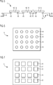
Ein Vorteil des beschriebenen optoelektronischen Bauelementes besteht darin, dass das Gehäuse mehrere Öffnungen zum Abgeben elektromagnetischer Strahlung aufweist. Die Öffnungen sind jeweils mit einer Platte abgedeckt. Die Platte besteht aus einem Material, das elektromagnetische Strahlung durchlässt. Durch die Anordnung mehrerer kleiner Öffnungen mit kleinen Platten wird im Gegensatz zu einer großen Öffnung mit einer großen Platte Material für die Platte eingespart. Zudem können kleinere Platten zuverlässiger mit dem Gehäuse verbunden werden. Insbesondere ist die langzeitstabile Verbindung zwischen den kleinen Platten und dem Gehäuse besser. Aufgrund der kleineren Form der einzelnen Platten sind beispielsweise thermische Spannungen zwischen der Platte und dem Gehäuse geringer. Somit wird die Befestigung zwischen der Platte und dem Gehäuse einem geringeren mechanischen Stress ausgesetzt. Weiterhin ist das Gehäuse stabiler ausgeführt, da im Gehäuse nicht eine einzige große Öffnung vorgesehen ist, sondern mehrere kleine Öffnungen vorgesehen sind. Die Platten bestehen aus einem teuren Material, sodass durch das Vorsehen mehrerer kleinerer Platten Plattenmaterial und damit Kosten eingespart werden. Das Gehäuse besteht aus einem kostengünstigeren Material. Somit ist das Bauelement insgesamt kostengünstiger herzustellen. An advantage of the described optoelectronic component is that the housing has a plurality of openings for emitting electromagnetic radiation. The openings are each covered with a plate. The plate is made of a material that transmits electromagnetic radiation. By arranging a plurality of small openings with small plates, material for the plate is saved in contrast to a large opening with a large plate. In addition, smaller plates can be more reliably connected to the housing. In particular, the long-term stable connection between the small plates and the housing is better. Due to the smaller shape of the individual plates, for example, thermal stresses between the plate and the housing are lower. Thus, the attachment between the plate and the housing is subjected to less mechanical stress. Furthermore, the housing is made more stable, since not a single large opening is provided in the housing, but a plurality of small openings are provided. The plates are made of an expensive material, so that the provision of several smaller plates plate material and thus save costs. The housing is made of a less expensive material. Thus, the device is overall less expensive to produce.
In einer Ausführungsform weist der Deckel im Bereich der Öffnungen jeweils eine Vertiefung auf, die durch eine Gehäusewand umgeben ist. Die Gehäusewand weist eine Auflagefläche auf, die die Öffnung umgibt. Die jeweilige Platte liegt auf der Auflagefläche auf und ist über eine Verbindungsschicht mit der Auflagefläche verbunden ist. Somit ist die Platte wenigstens teilweise in der Vertiefung angeordnet und wenigstens teilweise gegenüber der Oberseite des Gehäuses zurückversetzt. Auf diese Weise ist die Platte in der Vertiefung wenigstens teilweise gegenüber mechanischen Beschädigungen geschützt. In einer weiteren Ausführungsform weist die Vertiefung einen ähnlichen Querschnitt wie die Platte auf, wobei der Querschnitt der Vertiefung etwas größer gebildet ist als der Querschnitt der Platte. Dadurch wird der Montageaufwand reduziert, da keine separate Justierung der Platte in Bezug auf die Öffnung erforderlich ist. Bei der Montage wird die Platte einfach in die Vertiefung eingelegt. Durch die Ausbildung der Vertiefungen erfolgt eine automatische Justierung der Platten in Bezug auf die Öffnung, die von der Auflagefläche umgeben wird. Somit ist eine aufwändige Justierung der Position der Platte nicht erforderlich. Abhängig von der gewählten Ausführung können auch mehrere Öffnungen in einer Vertiefung ausgebildet sein. In one embodiment, the cover in the region of the openings in each case a depression which is surrounded by a housing wall. The housing wall has a bearing surface which surrounds the opening. The respective plate is located on the support surface and is connected via a connecting layer with the support surface. Thus, the plate is at least partially disposed in the recess and at least partially set back from the top of the housing. In this way, the plate in the recess is at least partially protected against mechanical damage. In a further embodiment, the recess has a similar cross section as the plate, wherein the cross section of the recess is formed slightly larger than the cross section of the plate. As a result, the installation effort is reduced because no separate adjustment of the plate is required with respect to the opening. During assembly, the plate is simply inserted into the recess. The formation of the depressions is an automatic adjustment of the plates with respect to the opening, which is surrounded by the support surface. Thus, a complex adjustment of the position of the plate is not required. Depending on the selected embodiment, a plurality of openings may be formed in a recess.
Zudem können auch mehrere Platten in einer Vertiefung angeordnet sein. In addition, several plates can be arranged in a recess.
Abhängig von der gewählten Ausführungsform ist die Vertiefung von der Strahlungsquelle weggerichtet. Die Vertiefung ist im Deckel des Gehäuses angeordnet und weist im Bereich der Seite des Deckels, die der Strahlungsquelle zugeordnet ist, eine größere Querschnittsfläche als die Öffnung auf. Auf diese Weise wird elektromagnetische Strahlung, die von der Strahlungsquelle ausgesandt wird, zuerst durch den breiteren Öffnungsquerschnitt der Vertiefung begrenzt. Anschließend wird die elektromagnetische Strahlung durch die Platte in Richtung der Öffnung weitergeführt. Die Öffnung selbst weist eine präzise Randkontur auf, die einen Strahlungskegel der Strahlungsquelle präzise festlegt und begrenzt. Somit wird eine verbesserte Strahlführung der elektromagnetischen Strahlung erreicht. Depending on the chosen embodiment, the recess is directed away from the radiation source. The depression is arranged in the cover of the housing and, in the region of the side of the cover which is assigned to the radiation source, has a larger cross-sectional area than the opening. In this way, electromagnetic radiation emitted by the radiation source is first limited by the wider opening cross-section of the recess. Subsequently, the electromagnetic radiation is continued through the plate in the direction of the opening. The opening itself has a precise edge contour, which precisely defines and limits a radiation cone of the radiation source. Thus, an improved beam guidance of the electromagnetic radiation is achieved.
In einer weiteren Ausführungsform ist die Vertiefung größer oder gleich der Dicke der Platte. Auf diese Weise kann die Platte vollständig in der Vertiefung aufgenommen werden. Somit wird bei der Anordnung mehrerer Platten nebeneinander eine Reflexion der einen Platte in Richtung auf eine benachbarte Platte vermieden werden. Auf diese Weise werden gegenseitige Streueffekte reduziert. In a further embodiment, the depression is greater than or equal to the thickness of the plate. In this way, the plate can be completely absorbed in the recess. Thus, in the arrangement of a plurality of plates side by side, a reflection of a plate in the direction of an adjacent plate can be avoided. In this way, mutual scattering effects are reduced.
In einer weiteren Ausführungsform weist das Gehäuse einen Rahmen auf, der den Deckel umlaufend umgibt. Der Rahmen weist eine umlaufende Kante auf, die mit der Trägerplatte verbunden ist. Durch die Ausbildung mehrerer Öffnungen ist ein größerer Abstand zwischen der umlaufenden Kante und den einzelnen Öffnungen, insbesondere den in der Mitte des Deckels angeordneten Öffnungen gegeben. Durch die Anordnung mehrerer Öffnungen weist die einzelne Öffnung einen größeren Abstand zur Kante auf. Die Kante wird nach der Montage der Platten mit der Trägerplatte über thermische Verfahren verbunden, insbesondere umlaufend hermetisch dicht verbunden. Beispielsweise kann die Verbindung in Form einer Schweißverbindung ausgebildet sein. Durch den größeren Abstand ist der thermische Effekt beim Verbinden der Kante mit der Trägerplatte auf die einzelne Platte der Öffnungen, insbesondere die Verbindung der Platte mit der Auflagefläche geringer. In a further embodiment, the housing has a frame which surrounds the cover circumferentially. The frame has a peripheral edge which is connected to the carrier plate. By forming a plurality of openings, a larger distance between the circumferential Edge and the individual openings, in particular given the arranged in the middle of the lid openings. By arranging a plurality of openings, the single opening has a greater distance from the edge. The edge is connected after assembly of the plates with the support plate via thermal processes, in particular hermetically sealed all around. For example, the connection may be in the form of a welded joint. Due to the larger distance, the thermal effect when connecting the edge to the carrier plate on the single plate of the openings, in particular the connection of the plate with the support surface is lower.
In einer weiteren Ausführungsform ist die Strahlungsquelle in Form einer Laserdiode ausgebildet. Beispielsweise können kleine Öffnungen den Vorteil bieten, dass eine Apertur der Strahlungsquelle eingegrenzt wird. In a further embodiment, the radiation source is designed in the form of a laser diode. For example, small openings may offer the advantage that an aperture of the radiation source is limited.
In einer weiteren Ausführungsform weist die Platte eine Vorrichtung, insbesondere eine Linse auf, um eine Ausbreitungsrichtung der elektromagnetischen Strahlung zu beeinflussen. Bei dieser Ausbildungsform kann sowohl die Platte selbst als Vorrichtung zur Beeinflussung der Ausbreitungsrichtung der elektromagnetischen Strahlung ausgebildet sein oder zusätzlich zur Platte kann eine Vorrichtung zur Beeinflussung der Ausbreitungsrichtung der elektromagnetischen Strahlung vorgesehen sein. Durch die Anordnung mehrerer Öffnungen ergibt sich die Möglichkeit, die einzelnen Platten mit unterschiedlichen Vorrichtungen zur Beeinflussung der elektromagnetischen Strahlung zu versehen. Somit können einzelne Strahlungsquellen in der Ausbreitungsrichtung unabhängig von den anderen Strahlungsquellen beeinflusst werden. In a further embodiment, the plate has a device, in particular a lens, in order to influence a propagation direction of the electromagnetic radiation. In this embodiment, both the plate itself may be formed as a device for influencing the propagation direction of the electromagnetic radiation or in addition to the plate may be provided a device for influencing the direction of propagation of the electromagnetic radiation. The arrangement of a plurality of openings affords the possibility of providing the individual plates with different devices for influencing the electromagnetic radiation. Thus, individual radiation sources in the propagation direction can be influenced independently of the other radiation sources.
In einer weiteren Ausführungsform sind den Öffnungen Vorrichtungen zugeordnet, um die Wellenlänge der elektromagnetischen Strahlung zu verändern. Auf diese Weise können die Wellenlängen einzelner Strahlungsquellen individuell eingestellt werden. Bei dieser Ausführungsform kann auch die Platte selbst als Vorrichtung zur Veränderung der Wellenlänge der elektromagnetischen Strahlung ausgebildet sein. Die Vorrichtung kann ausgebildet sein, um wenigstens einen Teil des Wellenlängenspektrums der Strahlungsquelle zu verschieben und/oder zu blockieren. In a further embodiment, the openings are associated with devices to change the wavelength of the electromagnetic radiation. In this way, the wavelengths of individual radiation sources can be adjusted individually. In this embodiment, the plate itself may be formed as a device for changing the wavelength of the electromagnetic radiation. The device may be configured to displace and / or block at least part of the wavelength spectrum of the radiation source.
In einer weiteren Ausführungsform sind die Platten mit dem Deckel hermetisch dicht verbunden. Auf diese Weise wird ein verbesserter Schutz der Strahlungsquellen erreicht. In a further embodiment, the plates are hermetically sealed to the lid. In this way, an improved protection of the radiation sources is achieved.
Abhängig von der gewählten Ausführungsform kann als Strahlungsquelle auch eine Laserbank mit mehreren Laserdioden vorgesehen sein. Bei dieser Ausführungsform können die Laserdioden einer Laserbank jeweils einer Öffnung zugeordnet sein. Zudem kann abhängig von der gewählten Ausführungsform das Bauelement in der Weise ausgebildet sein, dass jede Laserbank individuell angesteuert werden kann. Depending on the selected embodiment may be provided as a radiation source and a laser bank with a plurality of laser diodes. In this embodiment, the laser diodes of a laser bank may each be associated with an opening. In addition, depending on the selected embodiment, the component may be designed in such a way that each laser bank can be controlled individually.
In einer weiteren Ausführungsform ist der Deckel aus einem metallischen Material hergestellt. Zudem sind vorzugsweise die Vertiefungen mithilfe eines Tiefziehverfahren in die Metallplatte des Deckels eingebracht. Auf diese Weise wird eine kostengünstige Herstellung des Deckels möglich. Zudem wird durch die Vertiefungen eine versteifte Ausbildung des Deckels erreicht. In a further embodiment, the lid is made of a metallic material. In addition, the recesses are preferably introduced by means of a deep-drawing process in the metal plate of the lid. In this way, a cost-effective production of the lid is possible. In addition, a stiffened design of the lid is achieved by the wells.
In einer weiteren Ausführungsform ist der Rahmen des Gehäuses über eine umlaufende Schweißverbindung mit dem Träger verbunden. Die Schweißverbindung ermöglicht eine mechanisch stabile Verbindung zum Träger und bietet zudem eine hermetisch dichte Verbindung. In a further embodiment, the frame of the housing is connected to the carrier via a peripheral welded connection. The welded connection allows a mechanically stable connection to the carrier and also provides a hermetically sealed connection.
Die oben beschriebenen Eigenschaften, Merkmale und Vorteile dieser Erfindung sowie die Art und Weise, wie diese erreicht werden, werden klarer und deutlicher verständlich im Zusammenhang mit der folgenden Beschreibung der Ausführungsbeispiele, die im Zusammenhang mit den Zeichnungen näher erläutert werden, wobei The above-described characteristics, features, and advantages of this invention, as well as the manner in which they are achieved, will become clearer and more clearly understood in connection with the following description of the embodiments which will be described in connection with the drawings
Die Öffnungen
Beispielsweise kann für die Ausbildung des Gehäuses als Material ein metallischer Werkstoff verwendet werden. Zudem kann für die Ausbildung der Platte
Durch die Anordnung mehrerer Öffnungen
In der dargestellten Ausführungsform weisen die Vertiefungen
Auf diese Weise kann vermieden werden, dass elektromagnetische Strahlung von einer Platte
Der Deckel
Auf diese Weise kann beispielsweise aus einer Laserdiode mit einer elektromagnetischen Strahlung einer blauen Wellenlänge ein weißes Licht oder eine andere gewünschte Wellenlänge erzeugt werden. Abhängig von der gewählten Ausführungsform kann auch nur auf einer Seite der Platte
Weiterhin kann abhängig von der gewählten Ausführungsform auch eine Kombination der Anordnungen der
In einer weiteren Ausführungsform, die in
Abhängig von der gewählten Ausführungsform können in den verschiedenen Öffnungen
In einer weiteren Ausführungsform können in den Öffnungen
Anstelle von Phosphor können auch andere Materialien verwendet werden, um eine Filterung und/oder eine Verschiebung der Wellenlänge der elektromagnetischen Strahlung zu bewirken. Instead of phosphor, other materials may be used to effect filtering and / or shifting the wavelength of the electromagnetic radiation.
Zudem kann mithilfe der beschriebenen Ausführungsformen ein RGBY-Modul durch eine separate Ansteuerung einzelner Laserbänke der vier Reihen erreicht werden, das Licht in den Farben rot, grün, blau und gelb abstrahlt. Durch die definiert begrenzte Größe der Öffnung
Weiterhin kann durch das Vorsehen einzelner Öffnungen
Obwohl die Erfindung im Detail durch das bevorzugte Ausführungsbeispiel näher illustriert und beschrieben wurde, so ist die Erfindung nicht durch die offenbarten Beispiele eingeschränkt und andere Variationen können vom Fachmann hieraus abgeleitet werden, ohne den Schutzumfang der Erfindung zu verlassen. Although the invention has been further illustrated and described in detail by the preferred embodiment, the invention is not limited by the disclosed examples, and other variations can be derived therefrom by those skilled in the art without departing from the scope of the invention.
BezugszeichenlisteLIST OF REFERENCE NUMBERS
- 1 1
- Bauelement module
- 2 2
- Träger carrier
- 3 3
- erste Strahlungsquelle first radiation source
- 4 4
- zweite Strahlungsquelle second radiation source
- 5 5
- Gehäuse casing
- 6 6
- Rand edge
- 7 7
- Deckel cover
- 8 8th
- Randbereich border area
- 9 9
- Öffnung opening
- 10 10
- Platte plate
- 11 11
- Unterseite bottom
- 12 12
- Oberseite top
- 13 13
- Vertiefung deepening
- 14 14
- Gehäusewand housing wall
- 15 15
- Auflagefläche bearing surface
- 16 16
- Verbindungsschicht link layer
- 17 17
- Verbindungsfläche interface
- 18 18
- Kante edge
- 19 19
- erster Anschluss first connection
- 20 20
- zweiter Anschluss second connection
- 21 21
- erste Reihe first row
- 22 22
- zweite Reihe second row
- 23 23
- dritte Reihe third row
- 24 24
- vierte Reihe fourth row
- 25 25
- erste Schicht first shift
- 26 26
- zweite Schicht second layer
- 27 27
- Laserbarren laser bars
- 28 28
- Strahlungskegel radiation cone
- 2929
- Laserdiode laser diode
- 30 30
- Linse lens
Claims (15)
Priority Applications (3)
| Application Number | Priority Date | Filing Date | Title |
|---|---|---|---|
| DE102013209919.3A DE102013209919B4 (en) | 2013-05-28 | 2013-05-28 | Optoelectronic component with a package having multiple openings |
| PCT/EP2014/060973 WO2014191419A1 (en) | 2013-05-28 | 2014-05-27 | Optoelectronic component comprising a housing with a plurality of openings |
| US14/892,242 US10826277B2 (en) | 2013-05-28 | 2014-05-27 | Optoelectronic component having a housing with a plurality of openings |
Applications Claiming Priority (1)
| Application Number | Priority Date | Filing Date | Title |
|---|---|---|---|
| DE102013209919.3A DE102013209919B4 (en) | 2013-05-28 | 2013-05-28 | Optoelectronic component with a package having multiple openings |
Publications (2)
| Publication Number | Publication Date |
|---|---|
| DE102013209919A1 true DE102013209919A1 (en) | 2014-12-04 |
| DE102013209919B4 DE102013209919B4 (en) | 2025-06-26 |
Family
ID=50897556
Family Applications (1)
| Application Number | Title | Priority Date | Filing Date |
|---|---|---|---|
| DE102013209919.3A Active DE102013209919B4 (en) | 2013-05-28 | 2013-05-28 | Optoelectronic component with a package having multiple openings |
Country Status (3)
| Country | Link |
|---|---|
| US (1) | US10826277B2 (en) |
| DE (1) | DE102013209919B4 (en) |
| WO (1) | WO2014191419A1 (en) |
Cited By (1)
| Publication number | Priority date | Publication date | Assignee | Title |
|---|---|---|---|---|
| DE102018129346A1 (en) * | 2018-11-21 | 2020-05-28 | Osram Opto Semiconductors Gmbh | SEMICONDUCTOR LASER AND MANUFACTURING METHOD FOR A SEMICONDUCTOR LASER |
Families Citing this family (13)
| Publication number | Priority date | Publication date | Assignee | Title |
|---|---|---|---|---|
| JP6265055B2 (en) * | 2014-01-14 | 2018-01-24 | ソニー株式会社 | LIGHT EMITTING DEVICE, DISPLAY DEVICE, AND LIGHTING DEVICE |
| KR20150093283A (en) * | 2014-02-06 | 2015-08-18 | 삼성디스플레이 주식회사 | Frame and light source module comprising the same |
| CN112503404B (en) | 2015-05-20 | 2023-03-28 | 日亚化学工业株式会社 | Light emitting device |
| JP6288132B2 (en) * | 2015-05-20 | 2018-03-07 | 日亜化学工業株式会社 | Light emitting device |
| JP6780377B2 (en) * | 2016-08-30 | 2020-11-04 | 日亜化学工業株式会社 | Light emitting device |
| JP6792439B2 (en) * | 2016-12-19 | 2020-11-25 | 新光電気工業株式会社 | Cap member and its manufacturing method and light emitting device |
| JP6504193B2 (en) * | 2017-03-30 | 2019-04-24 | 日亜化学工業株式会社 | Light emitting device |
| JP6737760B2 (en) * | 2017-10-20 | 2020-08-12 | 日亜化学工業株式会社 | Light emitting device and lid used therefor |
| JP7071617B2 (en) * | 2017-10-20 | 2022-05-19 | 日亜化学工業株式会社 | Manufacturing method of semiconductor laser device |
| JP6755412B2 (en) * | 2017-10-31 | 2020-09-16 | 三菱電機株式会社 | Laser light source device and its manufacturing method |
| CN121748921A (en) * | 2020-05-14 | 2026-03-27 | 新唐科技日本株式会社 | Light source module |
| JP7469985B2 (en) * | 2020-08-05 | 2024-04-17 | シャープ福山レーザー株式会社 | Light-emitting device and light-emitting device set |
| JP7288221B2 (en) * | 2021-06-01 | 2023-06-07 | 日亜化学工業株式会社 | light emitting device |
Citations (8)
| Publication number | Priority date | Publication date | Assignee | Title |
|---|---|---|---|---|
| DE10008240A1 (en) * | 1999-02-24 | 2000-10-05 | Denso Corp | Semiconductor light projector has several light emitting devices projecting light towards a projection surface |
| DE20314391U1 (en) * | 2003-09-16 | 2003-12-18 | Everlight Electronics Europe Gmbh | Light emitting diode display element has a substrate with LED elements and printed circuit that are viewed through a protective cover |
| JP2007019301A (en) * | 2005-07-08 | 2007-01-25 | Fujifilm Holdings Corp | Optical multiplexing laser source and adjusting method thereof |
| JP2008091234A (en) * | 2006-10-03 | 2008-04-17 | Sanyo Electric Co Ltd | Electronic equipment |
| US20080291954A1 (en) * | 2005-11-29 | 2008-11-27 | Elta Systems Ltd. | Optical Projection System and Method for a Cooled Light Source |
| JP2009099633A (en) * | 2007-10-13 | 2009-05-07 | Nichia Corp | Semiconductor light emitting device |
| US7751458B2 (en) * | 2007-11-16 | 2010-07-06 | Fraunhofer Usa, Inc. Center For Laser Technology | High power laser diode array comprising at least one high power diode laser and laser light source comprising the same |
| JP2010199357A (en) * | 2009-02-26 | 2010-09-09 | Nichia Corp | Light emitting device and method for manufacturing the same |
Family Cites Families (28)
| Publication number | Priority date | Publication date | Assignee | Title |
|---|---|---|---|---|
| US6526653B1 (en) * | 1999-12-08 | 2003-03-04 | Amkor Technology, Inc. | Method of assembling a snap lid image sensor package |
| US6483030B1 (en) * | 1999-12-08 | 2002-11-19 | Amkor Technology, Inc. | Snap lid image sensor package |
| US6603183B1 (en) * | 2001-09-04 | 2003-08-05 | Amkor Technology, Inc. | Quick sealing glass-lidded package |
| US7662094B2 (en) * | 2002-05-14 | 2010-02-16 | Given Imaging Ltd. | Optical head assembly with dome, and device for use thereof |
| JP4002207B2 (en) * | 2003-04-21 | 2007-10-31 | 株式会社小糸製作所 | Vehicle headlamp |
| JP4245968B2 (en) | 2003-04-23 | 2009-04-02 | 株式会社小糸製作所 | Vehicle headlamp |
| US7653099B2 (en) * | 2004-06-02 | 2010-01-26 | Panasonic Corporation | Semiconductor laser device which is capable of stably emitting short-wavelength laser light |
| JP2006106504A (en) * | 2004-10-07 | 2006-04-20 | Nippon Electric Glass Co Ltd | Optical cap component |
| JP4812543B2 (en) | 2006-06-28 | 2011-11-09 | 株式会社小糸製作所 | Vehicle lighting |
| US7737636B2 (en) * | 2006-11-09 | 2010-06-15 | Intematix Corporation | LED assembly with an LED and adjacent lens and method of making same |
| JP2008140667A (en) * | 2006-12-01 | 2008-06-19 | Harison Toshiba Lighting Corp | Lighting device |
| US7942556B2 (en) * | 2007-06-18 | 2011-05-17 | Xicato, Inc. | Solid state illumination device |
| JP2009086075A (en) * | 2007-09-28 | 2009-04-23 | Alps Electric Co Ltd | Lens with lens barrel |
| JP5079474B2 (en) * | 2007-11-29 | 2012-11-21 | シャープ株式会社 | Cap member and semiconductor device using the same |
| US7717591B2 (en) * | 2007-12-27 | 2010-05-18 | Lumination Llc | Incorporating reflective layers into LED systems and/or components |
| TW201000819A (en) * | 2008-06-30 | 2010-01-01 | Create Electronic Optical Co Ltd | LED illumination device |
| JP2010251686A (en) * | 2009-03-26 | 2010-11-04 | Harison Toshiba Lighting Corp | Light emitting device and manufacturing method thereof |
| US8469548B2 (en) * | 2009-09-16 | 2013-06-25 | Ningbo Futai Electric CO., LTD. | Flash light with adjustable light arrangement |
| JP5471410B2 (en) * | 2009-12-18 | 2014-04-16 | 三菱電機株式会社 | Lens pressing spring and laser light source device using lens pressing spring |
| EP2354641A3 (en) * | 2010-01-26 | 2013-04-17 | Toshiba Lighting & Technology Corporation | Illumination apparatus |
| IT1399490B1 (en) * | 2010-04-09 | 2013-04-19 | Bevilacqua De | LED LIGHTING DEVICE |
| JP5910508B2 (en) * | 2011-01-07 | 2016-04-27 | 日本電気株式会社 | Laser light source module |
| CN103703302B (en) * | 2011-07-26 | 2016-08-17 | Lg伊诺特有限公司 | Light emitting module |
| US20130033851A1 (en) * | 2011-08-07 | 2013-02-07 | Yu-Chin Wang | Aquarium led lighting device |
| US9018747B2 (en) * | 2011-08-22 | 2015-04-28 | Kyocera Corporation | Optical semiconductor apparatus |
| US8806743B2 (en) * | 2012-08-07 | 2014-08-19 | Excelitas Technologies Singapore Pte. Ltd | Panelized process for SMT sensor devices |
| EP2765570A1 (en) * | 2013-02-06 | 2014-08-13 | Weidmann Plastics Technology AG | Illuminated display element and method for manufacturing such a display element |
| DE102013104964A1 (en) * | 2013-05-14 | 2014-11-20 | Micro-Hybrid Electronic Gmbh | Hermetically gas-tight optoelectronic or electro-optical component and method for its production |
-
2013
- 2013-05-28 DE DE102013209919.3A patent/DE102013209919B4/en active Active
-
2014
- 2014-05-27 WO PCT/EP2014/060973 patent/WO2014191419A1/en not_active Ceased
- 2014-05-27 US US14/892,242 patent/US10826277B2/en active Active
Patent Citations (8)
| Publication number | Priority date | Publication date | Assignee | Title |
|---|---|---|---|---|
| DE10008240A1 (en) * | 1999-02-24 | 2000-10-05 | Denso Corp | Semiconductor light projector has several light emitting devices projecting light towards a projection surface |
| DE20314391U1 (en) * | 2003-09-16 | 2003-12-18 | Everlight Electronics Europe Gmbh | Light emitting diode display element has a substrate with LED elements and printed circuit that are viewed through a protective cover |
| JP2007019301A (en) * | 2005-07-08 | 2007-01-25 | Fujifilm Holdings Corp | Optical multiplexing laser source and adjusting method thereof |
| US20080291954A1 (en) * | 2005-11-29 | 2008-11-27 | Elta Systems Ltd. | Optical Projection System and Method for a Cooled Light Source |
| JP2008091234A (en) * | 2006-10-03 | 2008-04-17 | Sanyo Electric Co Ltd | Electronic equipment |
| JP2009099633A (en) * | 2007-10-13 | 2009-05-07 | Nichia Corp | Semiconductor light emitting device |
| US7751458B2 (en) * | 2007-11-16 | 2010-07-06 | Fraunhofer Usa, Inc. Center For Laser Technology | High power laser diode array comprising at least one high power diode laser and laser light source comprising the same |
| JP2010199357A (en) * | 2009-02-26 | 2010-09-09 | Nichia Corp | Light emitting device and method for manufacturing the same |
Cited By (2)
| Publication number | Priority date | Publication date | Assignee | Title |
|---|---|---|---|---|
| DE102018129346A1 (en) * | 2018-11-21 | 2020-05-28 | Osram Opto Semiconductors Gmbh | SEMICONDUCTOR LASER AND MANUFACTURING METHOD FOR A SEMICONDUCTOR LASER |
| US12040588B2 (en) | 2018-11-21 | 2024-07-16 | Osram Opto Semiconductors Gmbh | Semiconductor laser and method for producing a semiconductor laser |
Also Published As
| Publication number | Publication date |
|---|---|
| WO2014191419A1 (en) | 2014-12-04 |
| US10826277B2 (en) | 2020-11-03 |
| US20160126704A1 (en) | 2016-05-05 |
| DE102013209919B4 (en) | 2025-06-26 |
Similar Documents
| Publication | Publication Date | Title |
|---|---|---|
| DE102013209919B4 (en) | Optoelectronic component with a package having multiple openings | |
| DE102012205513A1 (en) | Method for producing a radiation arrangement and radiation arrangement | |
| DE112009000987T5 (en) | Process for melting glass | |
| DE112009001296T5 (en) | Glass welding processes | |
| DE112009001347T5 (en) | Melt bonding process for glass | |
| DE19712828A1 (en) | Light curtain and process for its manufacture | |
| EP3984337B1 (en) | Explosion-proof housing with a reinforcing frame | |
| DE112013007654B4 (en) | display device | |
| EP3597020B1 (en) | Explosion-proof housing and method for producing same | |
| DE102017110317A1 (en) | Cover for an optoelectronic component and optoelectronic component | |
| DE102014112891A1 (en) | Optical element and optoelectronic component | |
| DE102008003971A1 (en) | Light-emitting diode arrangement with protective frame | |
| DE102016108776A1 (en) | Optical arrangement and display device | |
| DE1796038A1 (en) | Process for welding materials with glass or similar materials | |
| DE102014110282A1 (en) | Lighting device for vehicles | |
| DE102013214235A1 (en) | Lighting device with semiconductor light sources and circumferential dam | |
| DE102016109041A1 (en) | MODULE FOR A VIDEO WALL | |
| DE102014116687A1 (en) | Optoelectronic component and lighting device | |
| EP2747060B1 (en) | Indicator lamp | |
| DE102016215361A1 (en) | Housing and method for producing a housing | |
| DE102018211978A1 (en) | Mounting housing for a light-emitting element | |
| WO2018041943A1 (en) | Assembly comprising a radiation-emitting optoelectronic component | |
| EP2578930B1 (en) | Light module for an external light | |
| DE102016106135A1 (en) | Electronic unit | |
| EP2924343A1 (en) | Led light with refractive optics for mixing light |
Legal Events
| Date | Code | Title | Description |
|---|---|---|---|
| R163 | Identified publications notified | ||
| R012 | Request for examination validly filed | ||
| R016 | Response to examination communication | ||
| R016 | Response to examination communication | ||
| R016 | Response to examination communication | ||
| R018 | Grant decision by examination section/examining division | ||
| R020 | Patent grant now final |