DE102013208825B4 - Microstructure component and method for manufacturing a microstructure component - Google Patents
Microstructure component and method for manufacturing a microstructure component Download PDFInfo
- Publication number
- DE102013208825B4 DE102013208825B4 DE102013208825.6A DE102013208825A DE102013208825B4 DE 102013208825 B4 DE102013208825 B4 DE 102013208825B4 DE 102013208825 A DE102013208825 A DE 102013208825A DE 102013208825 B4 DE102013208825 B4 DE 102013208825B4
- Authority
- DE
- Germany
- Prior art keywords
- electrode
- substrate
- functional layer
- extension plane
- parallel
- Prior art date
- Legal status (The legal status is an assumption and is not a legal conclusion. Google has not performed a legal analysis and makes no representation as to the accuracy of the status listed.)
- Active
Links
- 238000004519 manufacturing process Methods 0.000 title claims description 40
- 238000000034 method Methods 0.000 title claims description 12
- 239000000758 substrate Substances 0.000 claims abstract description 80
- 230000001133 acceleration Effects 0.000 claims abstract description 8
- 239000002346 layers by function Substances 0.000 claims description 77
- 239000010410 layer Substances 0.000 claims description 30
- 230000010355 oscillation Effects 0.000 claims description 14
- 238000013016 damping Methods 0.000 description 14
- 238000011161 development Methods 0.000 description 10
- 230000018109 developmental process Effects 0.000 description 10
- 239000004020 conductor Substances 0.000 description 6
- 230000000694 effects Effects 0.000 description 5
- 238000005530 etching Methods 0.000 description 4
- WFKWXMTUELFFGS-UHFFFAOYSA-N tungsten Chemical compound [W] WFKWXMTUELFFGS-UHFFFAOYSA-N 0.000 description 4
- 229910052721 tungsten Inorganic materials 0.000 description 4
- 239000010937 tungsten Substances 0.000 description 4
- 230000035945 sensitivity Effects 0.000 description 3
- 229910052581 Si3N4 Inorganic materials 0.000 description 2
- 239000003990 capacitor Substances 0.000 description 2
- 239000003795 chemical substances by application Substances 0.000 description 2
- 229910052782 aluminium Inorganic materials 0.000 description 1
- XAGFODPZIPBFFR-UHFFFAOYSA-N aluminium Chemical compound [Al] XAGFODPZIPBFFR-UHFFFAOYSA-N 0.000 description 1
- 230000015572 biosynthetic process Effects 0.000 description 1
- 238000001514 detection method Methods 0.000 description 1
- 230000005496 eutectics Effects 0.000 description 1
- 238000011156 evaluation Methods 0.000 description 1
- 229910052732 germanium Inorganic materials 0.000 description 1
- GNPVGFCGXDBREM-UHFFFAOYSA-N germanium atom Chemical compound [Ge] GNPVGFCGXDBREM-UHFFFAOYSA-N 0.000 description 1
- 239000004922 lacquer Substances 0.000 description 1
- 229910052751 metal Inorganic materials 0.000 description 1
- 239000002184 metal Substances 0.000 description 1
- 238000004886 process control Methods 0.000 description 1
- HQVNEWCFYHHQES-UHFFFAOYSA-N silicon nitride Chemical compound N12[Si]34N5[Si]62N3[Si]51N64 HQVNEWCFYHHQES-UHFFFAOYSA-N 0.000 description 1
Images
Classifications
-
- G—PHYSICS
- G01—MEASURING; TESTING
- G01P—MEASURING LINEAR OR ANGULAR SPEED, ACCELERATION, DECELERATION, OR SHOCK; INDICATING PRESENCE, ABSENCE, OR DIRECTION, OF MOVEMENT
- G01P1/00—Details of instruments
- G01P1/003—Details of instruments used for damping
-
- G—PHYSICS
- G01—MEASURING; TESTING
- G01C—MEASURING DISTANCES, LEVELS OR BEARINGS; SURVEYING; NAVIGATION; GYROSCOPIC INSTRUMENTS; PHOTOGRAMMETRY OR VIDEOGRAMMETRY
- G01C19/00—Gyroscopes; Turn-sensitive devices using vibrating masses; Turn-sensitive devices without moving masses; Measuring angular rate using gyroscopic effects
- G01C19/56—Turn-sensitive devices using vibrating masses, e.g. vibratory angular rate sensors based on Coriolis forces
- G01C19/5719—Turn-sensitive devices using vibrating masses, e.g. vibratory angular rate sensors based on Coriolis forces using planar vibrating masses driven in a translation vibration along an axis
- G01C19/5733—Structural details or topology
- G01C19/5755—Structural details or topology the devices having a single sensing mass
-
- B—PERFORMING OPERATIONS; TRANSPORTING
- B81—MICROSTRUCTURAL TECHNOLOGY
- B81B—MICROSTRUCTURAL DEVICES OR SYSTEMS, e.g. MICROMECHANICAL DEVICES
- B81B3/00—Devices comprising flexible or deformable elements, e.g. comprising elastic tongues or membranes
- B81B3/0064—Constitution or structural means for improving or controlling the physical properties of a device
- B81B3/0067—Mechanical properties
- B81B3/0078—Constitution or structural means for improving mechanical properties not provided for in B81B3/007 - B81B3/0075
-
- G—PHYSICS
- G01—MEASURING; TESTING
- G01P—MEASURING LINEAR OR ANGULAR SPEED, ACCELERATION, DECELERATION, OR SHOCK; INDICATING PRESENCE, ABSENCE, OR DIRECTION, OF MOVEMENT
- G01P15/00—Measuring acceleration; Measuring deceleration; Measuring shock, i.e. sudden change of acceleration
- G01P15/02—Measuring acceleration; Measuring deceleration; Measuring shock, i.e. sudden change of acceleration by making use of inertia forces using solid seismic masses
- G01P15/08—Measuring acceleration; Measuring deceleration; Measuring shock, i.e. sudden change of acceleration by making use of inertia forces using solid seismic masses with conversion into electric or magnetic values
- G01P15/0802—Details
-
- G—PHYSICS
- G01—MEASURING; TESTING
- G01P—MEASURING LINEAR OR ANGULAR SPEED, ACCELERATION, DECELERATION, OR SHOCK; INDICATING PRESENCE, ABSENCE, OR DIRECTION, OF MOVEMENT
- G01P15/00—Measuring acceleration; Measuring deceleration; Measuring shock, i.e. sudden change of acceleration
- G01P15/02—Measuring acceleration; Measuring deceleration; Measuring shock, i.e. sudden change of acceleration by making use of inertia forces using solid seismic masses
- G01P15/08—Measuring acceleration; Measuring deceleration; Measuring shock, i.e. sudden change of acceleration by making use of inertia forces using solid seismic masses with conversion into electric or magnetic values
- G01P15/0888—Measuring acceleration; Measuring deceleration; Measuring shock, i.e. sudden change of acceleration by making use of inertia forces using solid seismic masses with conversion into electric or magnetic values for indicating angular acceleration
-
- G—PHYSICS
- G01—MEASURING; TESTING
- G01P—MEASURING LINEAR OR ANGULAR SPEED, ACCELERATION, DECELERATION, OR SHOCK; INDICATING PRESENCE, ABSENCE, OR DIRECTION, OF MOVEMENT
- G01P15/00—Measuring acceleration; Measuring deceleration; Measuring shock, i.e. sudden change of acceleration
- G01P15/02—Measuring acceleration; Measuring deceleration; Measuring shock, i.e. sudden change of acceleration by making use of inertia forces using solid seismic masses
- G01P15/08—Measuring acceleration; Measuring deceleration; Measuring shock, i.e. sudden change of acceleration by making use of inertia forces using solid seismic masses with conversion into electric or magnetic values
- G01P15/097—Measuring acceleration; Measuring deceleration; Measuring shock, i.e. sudden change of acceleration by making use of inertia forces using solid seismic masses with conversion into electric or magnetic values by vibratory elements
-
- G—PHYSICS
- G01—MEASURING; TESTING
- G01P—MEASURING LINEAR OR ANGULAR SPEED, ACCELERATION, DECELERATION, OR SHOCK; INDICATING PRESENCE, ABSENCE, OR DIRECTION, OF MOVEMENT
- G01P15/00—Measuring acceleration; Measuring deceleration; Measuring shock, i.e. sudden change of acceleration
- G01P15/02—Measuring acceleration; Measuring deceleration; Measuring shock, i.e. sudden change of acceleration by making use of inertia forces using solid seismic masses
- G01P15/08—Measuring acceleration; Measuring deceleration; Measuring shock, i.e. sudden change of acceleration by making use of inertia forces using solid seismic masses with conversion into electric or magnetic values
- G01P15/125—Measuring acceleration; Measuring deceleration; Measuring shock, i.e. sudden change of acceleration by making use of inertia forces using solid seismic masses with conversion into electric or magnetic values by capacitive pick-up
-
- B—PERFORMING OPERATIONS; TRANSPORTING
- B81—MICROSTRUCTURAL TECHNOLOGY
- B81B—MICROSTRUCTURAL DEVICES OR SYSTEMS, e.g. MICROMECHANICAL DEVICES
- B81B2201/00—Specific applications of microelectromechanical systems
- B81B2201/02—Sensors
- B81B2201/0228—Inertial sensors
- B81B2201/0235—Accelerometers
-
- B—PERFORMING OPERATIONS; TRANSPORTING
- B81—MICROSTRUCTURAL TECHNOLOGY
- B81B—MICROSTRUCTURAL DEVICES OR SYSTEMS, e.g. MICROMECHANICAL DEVICES
- B81B2201/00—Specific applications of microelectromechanical systems
- B81B2201/02—Sensors
- B81B2201/0228—Inertial sensors
- B81B2201/0242—Gyroscopes
-
- B—PERFORMING OPERATIONS; TRANSPORTING
- B81—MICROSTRUCTURAL TECHNOLOGY
- B81B—MICROSTRUCTURAL DEVICES OR SYSTEMS, e.g. MICROMECHANICAL DEVICES
- B81B2203/00—Basic microelectromechanical structures
- B81B2203/04—Electrodes
-
- B—PERFORMING OPERATIONS; TRANSPORTING
- B81—MICROSTRUCTURAL TECHNOLOGY
- B81B—MICROSTRUCTURAL DEVICES OR SYSTEMS, e.g. MICROMECHANICAL DEVICES
- B81B2203/00—Basic microelectromechanical structures
- B81B2203/05—Type of movement
- B81B2203/051—Translation according to an axis parallel to the substrate
-
- G—PHYSICS
- G01—MEASURING; TESTING
- G01P—MEASURING LINEAR OR ANGULAR SPEED, ACCELERATION, DECELERATION, OR SHOCK; INDICATING PRESENCE, ABSENCE, OR DIRECTION, OF MOVEMENT
- G01P15/00—Measuring acceleration; Measuring deceleration; Measuring shock, i.e. sudden change of acceleration
- G01P15/02—Measuring acceleration; Measuring deceleration; Measuring shock, i.e. sudden change of acceleration by making use of inertia forces using solid seismic masses
- G01P15/08—Measuring acceleration; Measuring deceleration; Measuring shock, i.e. sudden change of acceleration by making use of inertia forces using solid seismic masses with conversion into electric or magnetic values
- G01P2015/0805—Measuring acceleration; Measuring deceleration; Measuring shock, i.e. sudden change of acceleration by making use of inertia forces using solid seismic masses with conversion into electric or magnetic values being provided with a particular type of spring-mass-system for defining the displacement of a seismic mass due to an external acceleration
- G01P2015/0808—Measuring acceleration; Measuring deceleration; Measuring shock, i.e. sudden change of acceleration by making use of inertia forces using solid seismic masses with conversion into electric or magnetic values being provided with a particular type of spring-mass-system for defining the displacement of a seismic mass due to an external acceleration for defining in-plane movement of the mass, i.e. movement of the mass in the plane of the substrate
- G01P2015/0811—Measuring acceleration; Measuring deceleration; Measuring shock, i.e. sudden change of acceleration by making use of inertia forces using solid seismic masses with conversion into electric or magnetic values being provided with a particular type of spring-mass-system for defining the displacement of a seismic mass due to an external acceleration for defining in-plane movement of the mass, i.e. movement of the mass in the plane of the substrate for one single degree of freedom of movement of the mass
- G01P2015/0814—Measuring acceleration; Measuring deceleration; Measuring shock, i.e. sudden change of acceleration by making use of inertia forces using solid seismic masses with conversion into electric or magnetic values being provided with a particular type of spring-mass-system for defining the displacement of a seismic mass due to an external acceleration for defining in-plane movement of the mass, i.e. movement of the mass in the plane of the substrate for one single degree of freedom of movement of the mass for translational movement of the mass, e.g. shuttle type
-
- G—PHYSICS
- G01—MEASURING; TESTING
- G01P—MEASURING LINEAR OR ANGULAR SPEED, ACCELERATION, DECELERATION, OR SHOCK; INDICATING PRESENCE, ABSENCE, OR DIRECTION, OF MOVEMENT
- G01P15/00—Measuring acceleration; Measuring deceleration; Measuring shock, i.e. sudden change of acceleration
- G01P15/02—Measuring acceleration; Measuring deceleration; Measuring shock, i.e. sudden change of acceleration by making use of inertia forces using solid seismic masses
- G01P15/08—Measuring acceleration; Measuring deceleration; Measuring shock, i.e. sudden change of acceleration by making use of inertia forces using solid seismic masses with conversion into electric or magnetic values
- G01P2015/0862—Measuring acceleration; Measuring deceleration; Measuring shock, i.e. sudden change of acceleration by making use of inertia forces using solid seismic masses with conversion into electric or magnetic values being provided with particular means being integrated into a MEMS accelerometer structure for providing particular additional functionalities to those of a spring mass system
- G01P2015/0877—Measuring acceleration; Measuring deceleration; Measuring shock, i.e. sudden change of acceleration by making use of inertia forces using solid seismic masses with conversion into electric or magnetic values being provided with particular means being integrated into a MEMS accelerometer structure for providing particular additional functionalities to those of a spring mass system using integrated interconnect structures
-
- G—PHYSICS
- G01—MEASURING; TESTING
- G01P—MEASURING LINEAR OR ANGULAR SPEED, ACCELERATION, DECELERATION, OR SHOCK; INDICATING PRESENCE, ABSENCE, OR DIRECTION, OF MOVEMENT
- G01P15/00—Measuring acceleration; Measuring deceleration; Measuring shock, i.e. sudden change of acceleration
- G01P15/02—Measuring acceleration; Measuring deceleration; Measuring shock, i.e. sudden change of acceleration by making use of inertia forces using solid seismic masses
- G01P15/08—Measuring acceleration; Measuring deceleration; Measuring shock, i.e. sudden change of acceleration by making use of inertia forces using solid seismic masses with conversion into electric or magnetic values
- G01P2015/0862—Measuring acceleration; Measuring deceleration; Measuring shock, i.e. sudden change of acceleration by making use of inertia forces using solid seismic masses with conversion into electric or magnetic values being provided with particular means being integrated into a MEMS accelerometer structure for providing particular additional functionalities to those of a spring mass system
- G01P2015/088—Measuring acceleration; Measuring deceleration; Measuring shock, i.e. sudden change of acceleration by making use of inertia forces using solid seismic masses with conversion into electric or magnetic values being provided with particular means being integrated into a MEMS accelerometer structure for providing particular additional functionalities to those of a spring mass system for providing wafer-level encapsulation
-
- G—PHYSICS
- G01—MEASURING; TESTING
- G01P—MEASURING LINEAR OR ANGULAR SPEED, ACCELERATION, DECELERATION, OR SHOCK; INDICATING PRESENCE, ABSENCE, OR DIRECTION, OF MOVEMENT
- G01P15/00—Measuring acceleration; Measuring deceleration; Measuring shock, i.e. sudden change of acceleration
- G01P15/02—Measuring acceleration; Measuring deceleration; Measuring shock, i.e. sudden change of acceleration by making use of inertia forces using solid seismic masses
- G01P15/08—Measuring acceleration; Measuring deceleration; Measuring shock, i.e. sudden change of acceleration by making use of inertia forces using solid seismic masses with conversion into electric or magnetic values
- G01P2015/0862—Measuring acceleration; Measuring deceleration; Measuring shock, i.e. sudden change of acceleration by making use of inertia forces using solid seismic masses with conversion into electric or magnetic values being provided with particular means being integrated into a MEMS accelerometer structure for providing particular additional functionalities to those of a spring mass system
- G01P2015/0882—Measuring acceleration; Measuring deceleration; Measuring shock, i.e. sudden change of acceleration by making use of inertia forces using solid seismic masses with conversion into electric or magnetic values being provided with particular means being integrated into a MEMS accelerometer structure for providing particular additional functionalities to those of a spring mass system for providing damping of vibrations
Landscapes
- Physics & Mathematics (AREA)
- General Physics & Mathematics (AREA)
- Engineering & Computer Science (AREA)
- Mechanical Engineering (AREA)
- Radar, Positioning & Navigation (AREA)
- Remote Sensing (AREA)
- Computer Hardware Design (AREA)
- Microelectronics & Electronic Packaging (AREA)
- Micromachines (AREA)
Abstract
Mikrostrukturbauelement (1), insbesondere zum Erfassen von Beschleunigungen und/oder Drehraten, mit einem eine Substrathaupterstreckungsebene (100) aufweisenden Substrat (10), einer Elektrode (30, 30') und einer weiteren Elektrode (30"), wobei die Elektrode (30, 30') eine Elektrodenhaupterstreckungsebene (300) und die weitere Elektrode (30") eine weitere Elektrodenhaupterstreckungsebene (300") aufweist, wobei die Elektrodenhaupterstreckungsebene (300) parallel zu einer zur Substrathaupterstreckungsebene (100) senkrechten Normalrichtung (103) angeordnet ist, wobei die weitere Elektrodenhaupterstreckungsebene (300") parallel zur Normalrichtung (103) angeordnet ist, wobei die Elektrode (30, 30') eine sich in die Normalrichtung (103) erstreckende Elektrodenhöhe (303) aufweist, wobei die Elektrode (30, 30') einen sich parallel zur Substrathaupterstreckungsebene (100) vollständig durch die Elektrode (30, 30') hindurch erstreckenden Strömungskanal (33) aufweist, wobei der Strömungskanal (33) eine sich parallel zur Normalrichtung (103) erstreckende Kanaltiefe (333) aufweist, wobei die Kanaltiefe (333) kleiner ist als die Elektrodenhöhe (303), wobei die Elektrode (30, 30') eine Elektrodenhaupterstreckungsrichtung (301) parallel zur Elektrodenhaupterstreckungsebene (300) und parallel zur Substrathaupterstreckungsebene (100) aufweist, dadurch gekennzeichnet, dass die Elektrode (30, 30') mehrere entlang der Elektrodenhaupterstreckungsrichtung (301) angeordnete Strömungskanäle (33) aufweist, wobei die Elektrode (30, 30') eine Mehrzahl von durch die mehreren Strömungskanäle (33) voneinander beabstandete Teilelektroden (32) aufweist, wobei die Teilelektroden (32) auf einem gemeinsamen Träger (34) angeordnet sind.Microstructure component (1), in particular for detecting accelerations and / or rotation rates, with a substrate (10) having a substrate main plane (100), an electrode (30, 30 ') and a further electrode (30 "), the electrode (30 , 30 ') has an electrode main extension plane (300) and the further electrode (30 ") has a further electrode main extension plane (300"), the electrode main extension plane (300) being arranged parallel to a normal direction (103) perpendicular to the substrate main extension plane (100) further electrode main extension plane (300 ") is arranged parallel to the normal direction (103), the electrode (30, 30 ') having an electrode height (303) extending in the normal direction (103), the electrode (30, 30') being one has a flow channel (33) extending parallel to the substrate main extension plane (100) completely through the electrode (30, 30 '), the flow channel (33) has a channel depth (333) extending parallel to the normal direction (103), the channel depth (333) being smaller than the electrode height (303), the electrode (30, 30 ') having a main electrode extension direction (301) parallel to the main electrode extension plane (300) and parallel to the substrate main extension plane (100), characterized in that the electrode (30, 30 ') has several flow channels (33) arranged along the electrode main extension direction (301), the electrode (30, 30') having a plurality of through the several Flow channels (33) has spaced-apart partial electrodes (32), wherein the partial electrodes (32) are arranged on a common carrier (34).
Description
Stand der TechnikState of the art
Die Erfindung geht aus von einem Mikrostrukturbauelement nach dem Oberbegriff des Anspruchs 1.The invention is based on a microstructure component according to the preamble of claim 1.
Solche Mikrostrukturbauelemente sind allgemein bekannt. Beispielsweise werden als mikromechanische Inertialsensoren ausgebildete Mikrostrukturbauelemente zur Messung von Beschleunigungen und Drehraten für verschiedene Applikationen im Automobilbereich und/oder im Verbrauchsgüterkauf in Massenfertigung hergestellt. Üblicherweise weisen die Inertialsensoren Elektrodenanordnungen zur Detektion einer Kapazitätsänderung auf, wobei die Kapazitätsänderung ein Maß für eine auf eine Inertialmasse des Inertialsensors wirkende Inertialkraft ist. Beispielsweise ist eine Inertialkraft eine Beschleunigungskraft und/oder eine Corioliskraft eines Beschleunigungssensors und/oder eines Drehratensensors. Die Elektrodenanordnung weist beispielsweise zwei Plattenelektroden mit jeweils parallel zueinander angeordneten Elektrodenhaupterstreckungsebenen auf, wobei eine der Plattenelektroden entlang einer zur Elektrodenhaupterstreckungsebene senkrechten Schwingungsrichtung zu einer Schwingung antreibbar ist. Die Schwingungsrichtung ist hierbei beispielsweise parallel zu einer Substrathaupterstreckungsebene eines Substrats des Mikrostrukturbauelements angeordnet. Die Elektrodenanordnung ist üblicherweise in einer hermetisch abgedichteten Kaverne oder Hohlraum des Mikrostrukturbauelements angeordnet, wobei in der Kaverne ein vergleichsweise geringer Kavernendruck herrscht. Mit zunehmender Schichtdicke bzw. Elektrodenhöhe entlang einer zur Substrathaupterstreckungsebene senkrechten Normalrichtung wirken sich Randströmeffekte und Dämpfungseffekte, beispielsweise die sogenannte Quetschfilmdämpfung, negativ auf Güte, Signalrauschen und/oder Offset aus.Such microstructure components are generally known. For example, microstructure components designed as micromechanical inertial sensors for measuring accelerations and rotation rates for various applications in the automotive sector and / or in consumer goods sales are mass-produced. The inertial sensors usually have electrode arrangements for detecting a change in capacitance, the change in capacitance being a measure of an inertial force acting on an inertial mass of the inertial sensor. For example, an inertial force is an acceleration force and / or a Coriolis force of an acceleration sensor and / or a rotation rate sensor. The electrode arrangement has, for example, two plate electrodes, each with electrode main extension planes arranged parallel to one another, wherein one of the plate electrodes can be driven to oscillate along an oscillation direction perpendicular to the electrode main extension plane. In this case, the direction of oscillation is arranged, for example, parallel to a substrate main plane of extent of a substrate of the microstructure component. The electrode arrangement is usually arranged in a hermetically sealed cavity or cavity of the microstructure component, with a comparatively low cavity pressure prevailing in the cavity. With increasing layer thickness or electrode height along a normal direction perpendicular to the main plane of extent of the substrate, edge current effects and damping effects, for example so-called squeeze film damping, have a negative effect on quality, signal noise and / or offset.
Die
Offenbarung der ErfindungDisclosure of the invention
Es ist daher Aufgabe der vorliegenden Erfindung ein Mikrostrukturbauelement und ein Verfahren zur Herstellung eines Mikrostrukturbauelements bereitzustellen, wobei bei einem gegebenen Kavernendruck Dämpfungskräfte in der Elektrodenanordnung gegenüber dem Stand der Technik reduziert und die mechanische Güte erhöht wird und/oder wobei die elektrische Empfindlichkeit der Elektrodenanordnung verbessert wird, ohne die Dämpfungskräfte zu erhöhen.It is therefore the object of the present invention to provide a microstructure component and a method for producing a microstructure component, with a given cavity pressure reducing damping forces in the electrode arrangement compared to the prior art and increasing the mechanical quality and / or improving the electrical sensitivity of the electrode arrangement without increasing the damping forces.
Das erfindungsgemäße Mikrostrukturbauelement und das erfindungsgemäße Verfahren zur Herstellung eines Mikrostrukturbauelements gemäß den nebengeordneten Ansprüchen haben gegenüber dem Stand der Technik den Vorteil, dass durch die Einführung eines oder mehrerer Strömungskanäle, welche sich jeweils durch die, insbesondere als Plattenelektrode ausgebildete, Elektrode parallel zur Substrathaupterstreckungsebene und/oder senkrecht zur Elektrodenhaupterstreckungsebene, vollständig durch die Elektrode hindurch erstrecken, austretende Gasmoleküle beim Auftreten der Quetschfilmdämpfung durch die Strömungskanäle entweichen können, sodass auf die Elektroden wirkende Dämpfungskräfte im Vergleich zu Elektroden ohne Strömungskanal erheblich reduziert werden. Die Ausbildung der Strömungskanäle der Elektrode bewirkt in vorteilhafter Weise, dass die Empfindlichkeit der Elektrodenanordnung, welche nachfolgend auch als Kondensatoranordnung bezeichnet wird, nur geringfügig sinkt. Ein Teil der fehlenden Kondensatorfläche wird besonders vorteilhaft durch Streufeldanteile von den Seitenflächen der geschlitzten Elektrode bzw. den Strömungskanal aufweisenden Elektrode kompensiert. Somit wird durch eine Vergrößerung der Elektrodenhöhe die Empfindlichkeit der Elektrodenanordnung bezüglich der Detektion der Kapazitätsänderung verbessert, wobei die Dämpfungseffekte nur geringfügig oder gar nicht mit zunehmender Elektrodenhöhe zunehmen. Besonders bevorzugt durchdringen die Strömungskanäle, welche hier auch Schlitze genannte werden, die Elektrodenhöhe die Elektrode parallel zur Substrathaupterstreckungsebene, und insbesondere senkrecht zur Elektrodenhaupterstreckungsebene vollständig, wobei insbesondere der Kanalabstand im Falle von mindestens zwei an der Elektrode angeordneten Strömungskanälen bevorzugt kleiner als die Elektrodenhöhe oder gleich der Elektrodenhöhe ist. Bevorzugt erstreckt sich die Kanaltiefe über mehr als 50% der Elektrodenhöhe entlang der Normalrichtung. Alternativ zu einer verglichen mit der Elektrodenhöhe kleineren Kanaltiefe ist die Kanaltiefe insbesondere gleich der Elektrodenhöhe.The microstructure component according to the invention and the method according to the invention for producing a microstructure component according to the independent claims have the advantage over the prior art that, through the introduction of one or more flow channels, each of which extends through the electrode, in particular designed as a plate electrode, parallel to the substrate main extension plane and / or perpendicular to the main plane of extension of the electrode, extending completely through the electrode, escaping gas molecules can escape through the flow channels when the squeeze film damping occurs, so that damping forces acting on the electrodes are considerably reduced compared to electrodes without a flow channel. The formation of the flow channels of the electrode has the advantageous effect that the sensitivity of the electrode arrangement, which is also referred to below as the capacitor arrangement, only drops slightly. Part of the missing capacitor surface is particularly advantageously compensated for by stray field components from the side surfaces of the slotted electrode or the electrode having the flow channel. Thus, by increasing the electrode height, the sensitivity of the electrode arrangement with regard to the detection of the change in capacitance is improved, the damping effects increasing only slightly or not at all with increasing electrode height. Particularly preferably, the flow channels, which are also called slots here, penetrate the electrode height completely through the electrode parallel to the substrate main extension plane, and in particular perpendicular to the electrode main extension plane, in particular the channel spacing in the case of at least two flow channels arranged on the electrode preferably less than or equal to the electrode height Electrode height is. The channel depth preferably extends over more than 50% of the electrode height along the normal direction. As an alternative to a channel depth that is smaller compared to the electrode height, the channel depth is in particular equal to the electrode height.
Durch einen zweistufigen Trenchprozess des erfindungsgemäßen Verfahrens ist es weiterhin vorteilhaft möglich, einen Strömungskanal aus der Elektrode auszubilden, ohne die Elektrode durch die gesamte Schichtdicke der Funktionsschicht oder durch die gesamte Elektrodenhöhe in Normalrichtung zu ätzen. In dem zweiten Herstellungsschritt wird die Elektrodenstruktur - welche insbesondere die Elektrode, die weitere Elektrode und/oder die Inertialstruktur umfasst - bis zu einer ersten Strukturtiefe während des ersten Zeitintervalls aus der Funktionsschicht ausgebildet. Die Strukturtiefe, welche hier auch als Tiefe des ersten Trenches bezeichnet wird, wird über die Dauer des ersten Zeitintervalls bzw. der ersten Prozessführung bestimmt, was bedeutet, dass es hier keinen definierten Ätzstopp gibt. In dem dritten Herstellungsschritt wird die Elektrodenstruktur weiter geätzt, wobei nun aber zusätzlich die Strömungskanäle in der ersten Elektrode und/oder weiteren Elektrode ausgebildet bzw. geätzt werden. Um ein vollständiges Durchätzen der Funktionsschicht zu verhindern wird der dritte Herstellungsschritt nach dem zweiten Zeitintervall rechtzeitig beendet und eine starke Überätzung vermieden.By means of a two-stage trench process of the method according to the invention, it is also advantageously possible to form a flow channel from the electrode without etching the electrode through the entire layer thickness of the functional layer or through the entire electrode height in the normal direction. In the second production step, the electrode structure - which in particular comprises the electrode, the further electrode and / or the inertial structure - is up to a first Structure depth formed from the functional layer during the first time interval. The structure depth, which is also referred to here as the depth of the first trench, is determined over the duration of the first time interval or the first process control, which means that there is no defined etching stop here. In the third manufacturing step, the electrode structure is further etched, but the flow channels are now additionally formed or etched in the first electrode and / or further electrode. In order to prevent the functional layer from being completely etched through, the third manufacturing step is ended in good time after the second time interval and severe overetching is avoided.
Vorteilhafte Ausgestaltungen und Weiterbildungen der Erfindung sind den Unteransprüchen, sowie der Beschreibung unter Bezugnahme auf die Zeichnungen entnehmbar.Advantageous refinements and developments of the invention can be found in the subclaims and the description with reference to the drawings.
Gemäß einer bevorzugten Weiterbildung beträgt die Kanaltiefe zwischen 60% und 95%, bevorzugt zwischen 70% und 90%, ganz besonders bevorzugt ungefähr 80% der Elektrodenhöhe. Hierdurch ist es vorteilhaft möglich, die Elektrode durch die Anordnung mehrere Strömungskanäle einstückig mit einer Kammstruktur auszubilden, wobei mehrere zinkenförmige als Teilelektroden bezeichnete senkrecht zur Schwingungsrichtung und parallel zur Substrathaupterstreckungsebene durch die Strömungskanäle voneinander beabstandete Elektrodensegmente elektrisch leitfähig miteinander verbunden sind. Insbesondere sind alternativ die Teilelektroden auf einem gemeinsamen Träger angeordnet, wobei der Träger aus einer weiteren Funktionsschicht ausgebildet wird, welche von der Funktionsschicht verschieden ist, aus der die Elektrode ausgebildet ist.According to a preferred development, the channel depth is between 60% and 95%, preferably between 70% and 90%, very particularly preferably approximately 80% of the electrode height. This advantageously makes it possible to design the electrode in one piece with a comb structure through the arrangement of several flow channels, with several prong-shaped electrode segments, referred to as partial electrodes, being connected to one another in an electrically conductive manner perpendicular to the direction of oscillation and parallel to the main plane of extension of the substrate through the flow channels. In particular, the partial electrodes are alternatively arranged on a common carrier, the carrier being formed from a further functional layer which is different from the functional layer from which the electrode is formed.
Erfindungsgemäß weist die Elektrode eine Elektrodenhaupterstreckungsrichtung parallel zur Elektrodenhaupterstreckungsebene und parallel zur Substrathaupterstreckungsebene auf, wobei die Elektrode mehrere entlang der Elektrodenhaupterstreckungsrichtung angeordnete Strömungskanäle aufweist. Gemäß einer bevorzugten Weiterbildung ist es insbesondere denkbar, dass die mehreren Strömungskanäle einen Kanalabstand aufweisen, wobei insbesondere der Kanalabstand kleiner als die Elektrodenhöhe ist. Hierdurch ist es vorteilhaft möglich, einen verbesserten Strömungspfad für die von der Quetschfilmdämpfung herrührenden austretenden Gasmoleküle bereitzustellen. Insbesondere ist vorteilhaft möglich, eine sich über sämtliche Elektroden der Elektrodenanordnung erstreckende Strömungskanalstruktur bereitzustellen.According to the invention, the electrode has a main electrode extension direction parallel to the main electrode extension plane and parallel to the main substrate extension plane, the electrode having a plurality of flow channels arranged along the main electrode extension direction. According to a preferred development, it is particularly conceivable that the plurality of flow channels have a channel spacing, the channel spacing in particular being smaller than the electrode height. This advantageously makes it possible to provide an improved flow path for the gas molecules emerging from the squeeze film damping. In particular, it is advantageously possible to provide a flow channel structure that extends over all electrodes of the electrode arrangement.
Erfindungsgemäß weist die Elektrode eine Mehrzahl von durch die mehreren Strömungskanäle voneinander beabstandete Teilelektroden auf, wobei die Teilelektroden auf einem gemeinsamen Träger angeordnet sind. Gemäß einer bevorzugten Weiterbildung ist es insbesondere möglich, dass die Elektrode aus einer Funktionsschicht ausgebildet ist, wobei der Träger insbesondere aus einer mit der Funktionsschicht verbundenen weiteren Funktionsschicht ausgebildet ist. Hierdurch ist es vorteilhaft möglich, eine platzsparende und Dämpfungskräfte reduzierende Elektrodenanordnung des Mikrostrukturbauelements bereitzustellen.According to the invention, the electrode has a plurality of partial electrodes spaced apart from one another by the plurality of flow channels, the partial electrodes being arranged on a common carrier. According to a preferred development, it is possible, in particular, for the electrode to be formed from a functional layer, the carrier in particular being formed from a further functional layer connected to the functional layer. This advantageously makes it possible to provide a space-saving electrode arrangement for the microstructure component that reduces damping forces.
Gemäß einer bevorzugten Weiterbildung sind die Teilelektroden über den Träger elektrisch leitfähig miteinander verbunden, wobei der Träger über, insbesondere genau, ein Elektrodenkontaktelement mit einem Leitungsmittel elektrisch leitfähig verbunden ist, wobei das Leitungsmittel auf dem Substrat angeordnet ist oder in einem mit dem Substrat verbundenen weiteren Substrat angeordnet ist, wobei das weitere Substrat insbesondere einen integrierten Schaltkreis umfasst. Hierdurch ist es vorteilhaft möglich, die Leitungsmittel bzw. den integrierten Schaltkreis unabhängig von der in der Funktionsschicht, und insbesondere weiteren Funktionsschicht, ausgebildeten Elektrodenanordnung zu strukturieren. Insbesondere ist es durch die Anbringung der Teilelektroden auf dem einen integrierten Schaltkreis umfassenden weiteren Substrat vorteilhaft möglich, eine Leitungsstruktur bereitzustellen, um eine Vielzahl, parallel zur Elektrodenhaupterstreckungsrichtung eine vergleichsweise geringe Länge aufweisende Teilelektroden anzuordnen.According to a preferred development, the partial electrodes are electrically conductively connected to one another via the carrier, the carrier being electrically conductively connected to a conduction means via, in particular precisely, an electrode contact element, the conduction means being arranged on the substrate or in a further substrate connected to the substrate is arranged, wherein the further substrate comprises in particular an integrated circuit. This advantageously makes it possible to structure the conduction means or the integrated circuit independently of the electrode arrangement formed in the functional layer, and in particular further functional layer. In particular, by attaching the partial electrodes to the further substrate comprising an integrated circuit, it is advantageously possible to provide a line structure in order to arrange a plurality of partial electrodes having a comparatively short length parallel to the main direction of extension of the electrodes.
Gemäß einer bevorzugten Weiterbildung ist die Elektrode relativ zum Substrat ortsfest angeordnet, wobei die weitere Elektrode relativ zum Substrat zu einer Bewegung entlang einer Schwingungsrichtung auslenkbar ist, wobei die Schwingungsrichtung insbesondere zur Substrathaupterstreckungsebene parallel angeordnet ist, wobei die Schwingungsrichtung insbesondere zur Elektrodenhaupterstreckungsebene und/oder zur weiteren Elektrodenhaupterstreckungsebene senkrecht angeordnet ist. Hierdurch ist es vorteilhaft möglich, die beweglichen Elektroden und/oder die festen Elektroden mit Strömungskanälen auszubilden, sodass die Gasmoleküle auf Grund der Quetschfilmdämpfung besonders effizient aus den Zwischenräumen zwischen der Elektrode und der weiteren Elektrode abzuleiten.According to a preferred development, the electrode is arranged in a stationary manner relative to the substrate, the further electrode being deflectable relative to the substrate to move along an oscillation direction, the oscillation direction in particular being arranged parallel to the substrate main extension plane, the oscillation direction in particular to the electrode main extension plane and / or to the further Electrode main extension plane is arranged vertically. This advantageously makes it possible to design the movable electrodes and / or the fixed electrodes with flow channels so that the gas molecules can be diverted particularly efficiently from the spaces between the electrode and the further electrode due to the squeeze film damping.
Gemäß einer bevorzugten Weiterbildung weist die weitere Elektrode parallel zur Normalrichtung die Elektrodenhöhe auf, wobei die weitere Elektrode einen sich parallel zur Substrathaupterstreckungsebene vollständig durch die weitere Elektrode hindurch erstreckenden weiteren Strömungskanal aufweist, wobei der weitere Strömungskanal eine sich parallel zur Normalrichtung erstreckende weitere Kanaltiefe aufweist, wobei die weitere Kanaltiefe kleiner ist als die Elektrodenhöhe, wobei insbesondere der Strömungskanal und der weitere Strömungskanal in eine entlang der Schwingungsrichtung verlaufende Projektionsrichtung in einer Reihe hintereinander oder versetzt nebeneinander angeordnet sind. Hierdurch ist es vorteilhaft möglich, die Quetschfilmdämpfungskräfte zu reduzieren und zugleich eine besonders stabile und platzsparende Elektrodenanordnung bereitzustellen.According to a preferred development, the further electrode has the electrode height parallel to the normal direction, the further electrode having a further flow channel extending completely through the further electrode parallel to the main plane of extension, the further flow channel having a further channel depth extending parallel to the normal direction, with the further channel depth is smaller than the electrode height, in particular the flow channel and the further Flow channel are arranged in a row one behind the other or offset next to one another in a projection direction running along the direction of vibration. This advantageously makes it possible to reduce the squeeze film damping forces and at the same time to provide a particularly stable and space-saving electrode arrangement.
Gemäß einer bevorzugten Weiterbildung des erfindungsgemäßen Verfahrens werden im zweiten Herstellungsschritt aus der Funktionsschicht in Abhängigkeit der zweiten Strukturierungsmaske die Elektrode mit einer Elektrodenhaupterstreckungsebene und die weitere Elektrode mit einer weiteren Elektrodenhaupterstreckungsebene ausgebildet, wobei die Elektrodenhaupterstreckungsebene parallel zur Normalrichtung angeordnet wird, wobei die weitere Elektrodenhaupterstreckungsebene parallel zur Normalrichtung angeordnet wird, wobei an der Elektrode eine sich in die Normalrichtung erstreckende Elektrodenhöhe ausgebildet wird. Hierdurch ist es vorteilhaft möglich, die Elektrodenstruktur mit der Elektrode, der weiteren Elektrode und/oder Inertialstruktur auszubilden, bevor die Strömungskanäle auf der Elektrode und/oder der weiteren Elektrode angeordnet werden. Hierdurch wird ein vergleichsweise einfaches und kostengünstiges Herstellungsverfahren bereitgestellt, um eine Vielzahl von Mikrostrukturbauelementen in einfacher Weise gleichzeitig herstellen zu können.According to a preferred development of the method according to the invention, in the second production step, the electrode with a main electrode extension plane and the further electrode with a further electrode main extension plane are formed from the functional layer depending on the second structuring mask, the electrode main extension plane being arranged parallel to the normal direction, the further electrode main extension plane being parallel to the normal direction is arranged, wherein an electrode height extending in the normal direction is formed on the electrode. This advantageously makes it possible to form the electrode structure with the electrode, the further electrode and / or inertial structure before the flow channels are arranged on the electrode and / or the further electrode. This provides a comparatively simple and inexpensive production method in order to be able to produce a large number of microstructure components in a simple manner at the same time.
Gemäß einer bevorzugten Weiterbildung des erfindungsgemäßen Verfahrens wird im dritten Herstellungsschritt aus der Elektrode in Abhängigkeit der ersten Strukturierungsmaske ein sich parallel zur Substrathaupterstreckungsebene vollständig durch die Elektrode hindurch erstreckender Strömungskanal mit einer sich parallel zur Normalrichtung erstreckenden Kanaltiefe ausgebildet, wobei die Kanaltiefe in Abhängigkeit des zweiten Zeitintervalls kleiner als die Elektrodenhöhe ausgebildet wird. Hierdurch ist es vorteilhaft möglich, durch eine Kombination der, insbesondere als Oxidmaske ausgebildeten, ersten Maske und der, insbesondere als Lackmaske ausgebildeten, zweiten Maske auf der eine vergleichsweise glatte Oberfläche parallel zur Substrathaupterstreckungsebene aufweisenden Funktionsschicht anzuordnen, um die Strömungskanäle mit einer Kanaltiefe kleiner als die Elektrodenhöhe in der Elektrode und/oder weiteren Elektrode auszubilden.According to a preferred development of the method according to the invention, in the third production step, a flow channel extending parallel to the main plane of extension of the substrate and extending completely through the electrode with a channel depth extending parallel to the normal direction is formed from the electrode as a function of the first structuring mask, the channel depth being smaller depending on the second time interval is formed as the electrode height. In this way, it is advantageously possible through a combination of the first mask, especially designed as an oxide mask, and the second mask, especially designed as a lacquer mask, to be arranged on the functional layer, which has a comparatively smooth surface parallel to the plane of the main extent of the substrate, in order to arrange the flow channels with a channel depth smaller than that Form electrode height in the electrode and / or further electrode.
Gemäß einer bevorzugten Weiterbildung des erfindungsgemäßen Verfahrens wird im dritten Herstellungsschritt die Funktionsschicht mit einer Funktionsschichtdicke bereitgestellt, wobei im vierten Herstellungsschritt der Strömungskanal mit der Kanaltiefe gleich der Funktionsschichtdicke ausgebildet wird. Insbesondere wird die Funktionsschicht in Normalrichtung über einer weiteren Funktionsschicht angeordnet, wobei zwischen der weiteren Funktionsschicht und der Funktionsschicht eine Strukturierungsmaske angeordnet wird. Insbesondere wird die Kanaltiefe des Strömungskanals durch die Lage der Strukturierungsmaske zwischen der Funktionsschicht und der weiteren Funktionsschicht bestimmt. Insbesondere ist die Strukturierungsmaske eine Ätzstoppschicht, welche die Kanaltiefe des Strömungskanals während des Ätzvorgangs begrenzt. Weiterhin werden hierdurch insbesondere eine Mehrzahl von Teilelektroden auf einem aus der weiteren Funktionsschicht ausgebildeten Träger bereitgestellt. Bevorzugt wird die Ätzstoppschicht in einem fünften Herstellungsschritt entfernt.According to a preferred development of the method according to the invention, the functional layer is provided with a functional layer thickness in the third manufacturing step, the flow channel being formed with the channel depth equal to the functional layer thickness in the fourth manufacturing step. In particular, the functional layer is arranged in the normal direction over a further functional layer, a structuring mask being arranged between the further functional layer and the functional layer. In particular, the channel depth of the flow channel is determined by the position of the structuring mask between the functional layer and the further functional layer. In particular, the structuring mask is an etch stop layer which limits the channel depth of the flow channel during the etching process. Furthermore, in this way, in particular, a plurality of partial electrodes are provided on a carrier formed from the further functional layer. The etch stop layer is preferably removed in a fifth production step.
Ausführungsbeispiele der vorliegenden Erfindung sind in den Zeichnungen dargestellt und in der nachfolgenden Beschreibung näher erläutert.Exemplary embodiments of the present invention are shown in the drawings and explained in more detail in the description below.
FigurenlisteFigure list
Es zeigen
-
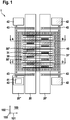
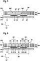
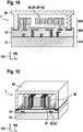
1 eine Schnittbildansicht eines Mikrostrukturbauelements zur Erläuterung der vorliegenden Erfindung, -
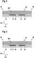
2 und3 Schnittbildansichten verschiedener Ausführungsformen einer Elektrode zur Erläuterung der vorliegenden Erfindung, -
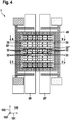
4 eine Draufsicht eines Mikrostrukturbauelements gemäß einer Ausführungsform der vorliegenden Erfindung, -
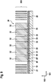
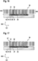
5 bis9 Schnittbildansichten verschiedener Ausführungsformen einer Elektrode gemäß der vorliegenden Erfindung, -
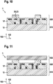
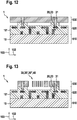
10 bis15 Schnittbildansichten eines Mikrostrukturbauelements gemäß einer Ausführungsform der vorliegenden Erfindung, -
16 bis17 Schnittbildansichten verschiedener Ausführungsformen einer Elektrode gemäß einer Ausführungsform der vorliegenden Erfindung, und -
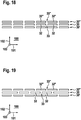
18 und19 Draufsichten verschiedener Ausführungsformen einer Anordnung der Strömungskanäle einer Elektrode gemäß der vorliegenden Erfindung.
-
1 a sectional view of a microstructure component to explain the present invention, -
2 and3 Sectional views of various embodiments of an electrode to explain the present invention, -
4th a top view of a microstructure component according to an embodiment of the present invention, -
5 to9 Sectional views of various embodiments of an electrode according to the present invention, -
10 to15th Sectional views of a microstructure component according to an embodiment of the present invention, -
16 to17th Sectional views of various embodiments of an electrode according to an embodiment of the present invention, and -
18th and19th Top views of various embodiments of an arrangement of the flow channels of an electrode according to the present invention.
Ausführungsform(en) der ErfindungEmbodiment (s) of the invention
In den verschiedenen Figuren sind gleiche Teile stets mit den gleichen Bezugszeichen versehen und werden daher in der Regel auch jeweils nur einmal benannt bzw. erwähnt.In the various figures, the same parts are always provided with the same reference numerals and are therefore usually only named or mentioned once.
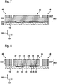
In
Die Inertialstruktur
In einem Zentralbereich weist die Inertialstruktur
In
In
In
In
In
In
In
Claims (12)
Priority Applications (2)
| Application Number | Priority Date | Filing Date | Title |
|---|---|---|---|
| DE102013208825.6A DE102013208825B4 (en) | 2013-05-14 | 2013-05-14 | Microstructure component and method for manufacturing a microstructure component |
| US14/120,386 US9229020B2 (en) | 2013-05-14 | 2014-05-14 | Micropatterned component and method for manufacturing a micropatterned component |
Applications Claiming Priority (1)
| Application Number | Priority Date | Filing Date | Title |
|---|---|---|---|
| DE102013208825.6A DE102013208825B4 (en) | 2013-05-14 | 2013-05-14 | Microstructure component and method for manufacturing a microstructure component |
Publications (2)
| Publication Number | Publication Date |
|---|---|
| DE102013208825A1 DE102013208825A1 (en) | 2014-11-20 |
| DE102013208825B4 true DE102013208825B4 (en) | 2021-05-20 |
Family
ID=51831291
Family Applications (1)
| Application Number | Title | Priority Date | Filing Date |
|---|---|---|---|
| DE102013208825.6A Active DE102013208825B4 (en) | 2013-05-14 | 2013-05-14 | Microstructure component and method for manufacturing a microstructure component |
Country Status (2)
| Country | Link |
|---|---|
| US (1) | US9229020B2 (en) |
| DE (1) | DE102013208825B4 (en) |
Families Citing this family (12)
| Publication number | Priority date | Publication date | Assignee | Title |
|---|---|---|---|---|
| DE102012210049A1 (en) * | 2012-06-14 | 2013-12-19 | Robert Bosch Gmbh | Hybrid integrated component and method for its production |
| US10273147B2 (en) | 2013-07-08 | 2019-04-30 | Motion Engine Inc. | MEMS components and method of wafer-level manufacturing thereof |
| JP6339669B2 (en) | 2013-07-08 | 2018-06-06 | モーション・エンジン・インコーポレーテッド | MEMS device and method of manufacturing |
| WO2015013827A1 (en) | 2013-08-02 | 2015-02-05 | Motion Engine Inc. | Mems motion sensor for sub-resonance angular rate sensing |
| WO2015103688A1 (en) | 2014-01-09 | 2015-07-16 | Motion Engine Inc. | Integrated mems system |
| US20170030788A1 (en) | 2014-04-10 | 2017-02-02 | Motion Engine Inc. | Mems pressure sensor |
| US11674803B2 (en) | 2014-06-02 | 2023-06-13 | Motion Engine, Inc. | Multi-mass MEMS motion sensor |
| US11287486B2 (en) | 2014-12-09 | 2022-03-29 | Motion Engine, Inc. | 3D MEMS magnetometer and associated methods |
| US10407299B2 (en) | 2015-01-15 | 2019-09-10 | Motion Engine Inc. | 3D MEMS device with hermetic cavity |
| DE102015222532A1 (en) * | 2015-11-16 | 2017-05-18 | Robert Bosch Gmbh | Micromechanical structure for an acceleration sensor |
| ITUA20162173A1 (en) | 2016-03-31 | 2017-10-01 | St Microelectronics Srl | ACCELEROMETRIC MEMS SENSOR HAVING HIGH ACCURACY AND REDUCED SENSITIVITY TOWARDS TEMPERATURE AND AGING |
| CN108801247B (en) * | 2018-06-04 | 2020-08-14 | 中北大学 | Low-temperature-drift resonant micro-accelerometer isosceles right-angle triangular array structure |
Citations (3)
| Publication number | Priority date | Publication date | Assignee | Title |
|---|---|---|---|---|
| US20030225362A1 (en) * | 2000-06-01 | 2003-12-04 | Currie John F. | Systems and methods for monitoring health and delivering drugs transdermally |
| US20050179099A1 (en) * | 2004-02-12 | 2005-08-18 | Markus Lutz | Integrated getter area for wafer level encapsulated microelectromechanical systems |
| DE102011007217A1 (en) * | 2010-04-12 | 2011-12-15 | Denso Corporation | A physical quantity detection device and method of manufacturing the same |
Family Cites Families (7)
| Publication number | Priority date | Publication date | Assignee | Title |
|---|---|---|---|---|
| US8227285B1 (en) * | 2008-06-25 | 2012-07-24 | MCube Inc. | Method and structure of monolithetically integrated inertial sensor using IC foundry-compatible processes |
| US9455354B2 (en) * | 2010-09-18 | 2016-09-27 | Fairchild Semiconductor Corporation | Micromachined 3-axis accelerometer with a single proof-mass |
| US9452924B2 (en) * | 2012-06-15 | 2016-09-27 | Taiwan Semiconductor Manufacturing Company, Ltd. | MEMS devices and fabrication methods thereof |
| US9174838B2 (en) * | 2012-12-10 | 2015-11-03 | MCube Inc. | Distributed MEMS devices time synchronization methods and system |
| DE102013217726B4 (en) * | 2013-09-05 | 2021-07-29 | Robert Bosch Gmbh | Micromechanical component for a capacitive sensor device and manufacturing method for a micromechanical component for a capacitive sensor device |
| US20150091911A1 (en) * | 2013-09-30 | 2015-04-02 | Pixtronix, Inc. | Movable mems element with stiction mitigating spring |
| US20150168146A1 (en) * | 2013-12-13 | 2015-06-18 | Sensors In Motion | Planar accelerometer with internal radial sensing and actuation |
-
2013
- 2013-05-14 DE DE102013208825.6A patent/DE102013208825B4/en active Active
-
2014
- 2014-05-14 US US14/120,386 patent/US9229020B2/en active Active
Patent Citations (3)
| Publication number | Priority date | Publication date | Assignee | Title |
|---|---|---|---|---|
| US20030225362A1 (en) * | 2000-06-01 | 2003-12-04 | Currie John F. | Systems and methods for monitoring health and delivering drugs transdermally |
| US20050179099A1 (en) * | 2004-02-12 | 2005-08-18 | Markus Lutz | Integrated getter area for wafer level encapsulated microelectromechanical systems |
| DE102011007217A1 (en) * | 2010-04-12 | 2011-12-15 | Denso Corporation | A physical quantity detection device and method of manufacturing the same |
Also Published As
| Publication number | Publication date |
|---|---|
| DE102013208825A1 (en) | 2014-11-20 |
| US9229020B2 (en) | 2016-01-05 |
| US20140339654A1 (en) | 2014-11-20 |
Similar Documents
| Publication | Publication Date | Title |
|---|---|---|
| DE102013208825B4 (en) | Microstructure component and method for manufacturing a microstructure component | |
| DE102012208032B4 (en) | Hybrid integrated component with MEMS component and ASIC component | |
| DE102012206854B4 (en) | Hybrid integrated component and process for its manufacture | |
| DE102012219550B4 (en) | Hybrid integrated component | |
| DE102006011545B4 (en) | Micromechanical combination component and corresponding manufacturing method | |
| DE102012200929B4 (en) | Micromechanical structure and method for manufacturing a micromechanical structure | |
| DE102013217726A1 (en) | Micromechanical component for a capacitive sensor device and method for producing a micromechanical component for a capacitive sensor device | |
| DE102012208033A1 (en) | Hybrid integrated component and method for its production | |
| DE102012217979A1 (en) | Hybrid integrated pressure sensor component | |
| DE102014215038B4 (en) | Micromechanical sensor and method for manufacturing a micromechanical sensor | |
| DE102013216901A1 (en) | Micromechanical component and method for producing a micromechanical component | |
| DE102012219465A1 (en) | Method for producing a cap for a MEMS component and hybrid integrated component with such a cap | |
| EP0494143B1 (en) | Device for measuring mechanical forces and dynamic effects | |
| DE102014202923A1 (en) | Sensor and method for producing a sensor | |
| DE102011011160B4 (en) | Micromechanical component and manufacturing process for a micromechanical component | |
| DE102010061782B4 (en) | Method for producing a micromechanical component | |
| DE102009026738A1 (en) | Micromechanical acceleration sensor and method for producing an acceleration sensor | |
| DE19530736B4 (en) | Acceleration sensor and method for manufacturing an acceleration sensor | |
| DE102006022379A1 (en) | Micromechanical pressure transducer for capacitive microelectromechanical system microphone, has substrate-sided cavity forming back volume for movable membrane, and resting at application-specific integrated circuit chip | |
| DE102013222836B4 (en) | 1Microelectromechanical component and corresponding manufacturing process | |
| WO2018041498A1 (en) | Micromechanical component comprising two membranes and method for producing a micromechanical component with two membranes | |
| DE102010062056B4 (en) | Micromechanical component | |
| DE102007050116B4 (en) | accelerometer | |
| DE102007013329B4 (en) | Method for producing a micromechanical component with a partial protective layer | |
| DE102024208643A1 (en) | Capacitive pressure sensor with a self-supporting sensing structure |
Legal Events
| Date | Code | Title | Description |
|---|---|---|---|
| R012 | Request for examination validly filed | ||
| R016 | Response to examination communication | ||
| R018 | Grant decision by examination section/examining division | ||
| R020 | Patent grant now final |