DE102013112721A1 - A method of driving an organic light emitting display device - Google Patents
A method of driving an organic light emitting display device Download PDFInfo
- Publication number
- DE102013112721A1 DE102013112721A1 DE102013112721.5A DE102013112721A DE102013112721A1 DE 102013112721 A1 DE102013112721 A1 DE 102013112721A1 DE 102013112721 A DE102013112721 A DE 102013112721A DE 102013112721 A1 DE102013112721 A1 DE 102013112721A1
- Authority
- DE
- Germany
- Prior art keywords
- scanned
- blocks
- data
- sequentially
- line
- Prior art date
- Legal status (The legal status is an assumption and is not a legal conclusion. Google has not performed a legal analysis and makes no representation as to the accuracy of the status listed.)
- Granted
Links
Images


Classifications
-
- G—PHYSICS
- G09—EDUCATION; CRYPTOGRAPHY; DISPLAY; ADVERTISING; SEALS
- G09G—ARRANGEMENTS OR CIRCUITS FOR CONTROL OF INDICATING DEVICES USING STATIC MEANS TO PRESENT VARIABLE INFORMATION
- G09G3/00—Control arrangements or circuits, of interest only in connection with visual indicators other than cathode-ray tubes
- G09G3/20—Control arrangements or circuits, of interest only in connection with visual indicators other than cathode-ray tubes for presentation of an assembly of a number of characters, e.g. a page, by composing the assembly by combination of individual elements arranged in a matrix no fixed position being assigned to or needed to be assigned to the individual characters or partial characters
- G09G3/22—Control arrangements or circuits, of interest only in connection with visual indicators other than cathode-ray tubes for presentation of an assembly of a number of characters, e.g. a page, by composing the assembly by combination of individual elements arranged in a matrix no fixed position being assigned to or needed to be assigned to the individual characters or partial characters using controlled light sources
- G09G3/30—Control arrangements or circuits, of interest only in connection with visual indicators other than cathode-ray tubes for presentation of an assembly of a number of characters, e.g. a page, by composing the assembly by combination of individual elements arranged in a matrix no fixed position being assigned to or needed to be assigned to the individual characters or partial characters using controlled light sources using electroluminescent panels
- G09G3/32—Control arrangements or circuits, of interest only in connection with visual indicators other than cathode-ray tubes for presentation of an assembly of a number of characters, e.g. a page, by composing the assembly by combination of individual elements arranged in a matrix no fixed position being assigned to or needed to be assigned to the individual characters or partial characters using controlled light sources using electroluminescent panels semiconductive, e.g. using light-emitting diodes [LED]
- G09G3/3208—Control arrangements or circuits, of interest only in connection with visual indicators other than cathode-ray tubes for presentation of an assembly of a number of characters, e.g. a page, by composing the assembly by combination of individual elements arranged in a matrix no fixed position being assigned to or needed to be assigned to the individual characters or partial characters using controlled light sources using electroluminescent panels semiconductive, e.g. using light-emitting diodes [LED] organic, e.g. using organic light-emitting diodes [OLED]
-
- G—PHYSICS
- G09—EDUCATION; CRYPTOGRAPHY; DISPLAY; ADVERTISING; SEALS
- G09G—ARRANGEMENTS OR CIRCUITS FOR CONTROL OF INDICATING DEVICES USING STATIC MEANS TO PRESENT VARIABLE INFORMATION
- G09G3/00—Control arrangements or circuits, of interest only in connection with visual indicators other than cathode-ray tubes
- G09G3/20—Control arrangements or circuits, of interest only in connection with visual indicators other than cathode-ray tubes for presentation of an assembly of a number of characters, e.g. a page, by composing the assembly by combination of individual elements arranged in a matrix no fixed position being assigned to or needed to be assigned to the individual characters or partial characters
- G09G3/22—Control arrangements or circuits, of interest only in connection with visual indicators other than cathode-ray tubes for presentation of an assembly of a number of characters, e.g. a page, by composing the assembly by combination of individual elements arranged in a matrix no fixed position being assigned to or needed to be assigned to the individual characters or partial characters using controlled light sources
- G09G3/30—Control arrangements or circuits, of interest only in connection with visual indicators other than cathode-ray tubes for presentation of an assembly of a number of characters, e.g. a page, by composing the assembly by combination of individual elements arranged in a matrix no fixed position being assigned to or needed to be assigned to the individual characters or partial characters using controlled light sources using electroluminescent panels
- G09G3/32—Control arrangements or circuits, of interest only in connection with visual indicators other than cathode-ray tubes for presentation of an assembly of a number of characters, e.g. a page, by composing the assembly by combination of individual elements arranged in a matrix no fixed position being assigned to or needed to be assigned to the individual characters or partial characters using controlled light sources using electroluminescent panels semiconductive, e.g. using light-emitting diodes [LED]
- G09G3/3208—Control arrangements or circuits, of interest only in connection with visual indicators other than cathode-ray tubes for presentation of an assembly of a number of characters, e.g. a page, by composing the assembly by combination of individual elements arranged in a matrix no fixed position being assigned to or needed to be assigned to the individual characters or partial characters using controlled light sources using electroluminescent panels semiconductive, e.g. using light-emitting diodes [LED] organic, e.g. using organic light-emitting diodes [OLED]
- G09G3/3225—Control arrangements or circuits, of interest only in connection with visual indicators other than cathode-ray tubes for presentation of an assembly of a number of characters, e.g. a page, by composing the assembly by combination of individual elements arranged in a matrix no fixed position being assigned to or needed to be assigned to the individual characters or partial characters using controlled light sources using electroluminescent panels semiconductive, e.g. using light-emitting diodes [LED] organic, e.g. using organic light-emitting diodes [OLED] using an active matrix
- G09G3/3233—Control arrangements or circuits, of interest only in connection with visual indicators other than cathode-ray tubes for presentation of an assembly of a number of characters, e.g. a page, by composing the assembly by combination of individual elements arranged in a matrix no fixed position being assigned to or needed to be assigned to the individual characters or partial characters using controlled light sources using electroluminescent panels semiconductive, e.g. using light-emitting diodes [LED] organic, e.g. using organic light-emitting diodes [OLED] using an active matrix with pixel circuitry controlling the current through the light-emitting element
-
- G—PHYSICS
- G09—EDUCATION; CRYPTOGRAPHY; DISPLAY; ADVERTISING; SEALS
- G09G—ARRANGEMENTS OR CIRCUITS FOR CONTROL OF INDICATING DEVICES USING STATIC MEANS TO PRESENT VARIABLE INFORMATION
- G09G2320/00—Control of display operating conditions
- G09G2320/02—Improving the quality of display appearance
- G09G2320/0233—Improving the luminance or brightness uniformity across the screen
-
- G—PHYSICS
- G09—EDUCATION; CRYPTOGRAPHY; DISPLAY; ADVERTISING; SEALS
- G09G—ARRANGEMENTS OR CIRCUITS FOR CONTROL OF INDICATING DEVICES USING STATIC MEANS TO PRESENT VARIABLE INFORMATION
- G09G2320/00—Control of display operating conditions
- G09G2320/02—Improving the quality of display appearance
- G09G2320/029—Improving the quality of display appearance by monitoring one or more pixels in the display panel, e.g. by monitoring a fixed reference pixel
- G09G2320/0295—Improving the quality of display appearance by monitoring one or more pixels in the display panel, e.g. by monitoring a fixed reference pixel by monitoring each display pixel
-
- G—PHYSICS
- G09—EDUCATION; CRYPTOGRAPHY; DISPLAY; ADVERTISING; SEALS
- G09G—ARRANGEMENTS OR CIRCUITS FOR CONTROL OF INDICATING DEVICES USING STATIC MEANS TO PRESENT VARIABLE INFORMATION
- G09G2320/00—Control of display operating conditions
- G09G2320/04—Maintaining the quality of display appearance
- G09G2320/043—Preventing or counteracting the effects of ageing
- G09G2320/045—Compensation of drifts in the characteristics of light emitting or modulating elements
Landscapes
- Engineering & Computer Science (AREA)
- Physics & Mathematics (AREA)
- Computer Hardware Design (AREA)
- General Physics & Mathematics (AREA)
- Theoretical Computer Science (AREA)
- Control Of El Displays (AREA)
- Electroluminescent Light Sources (AREA)
- Control Of Indicators Other Than Cathode Ray Tubes (AREA)
Abstract
Eine organische Licht emittierende Anzeigevorrichtung umfasst eine Anzeigetafel (100) mit einer Vielzahl von Pixeln (P), die mit einer Pixelschaltung zur Verfügung gestellt sind, um eine organische Licht emittierende Diode zu betreiben, und einer Treiberschaltung, um die Anzeigetafel (100) zu treiben, wobei 'n' horizontale Abtastleitungen in der Anzeigetafel (100) ausgebildet sind, und das Verfahren zum Treiben der Anzeigevorrichtung (100) umfasst: Teilen der 'n' horizontalen Abtastleitungen, die in der Anzeigetafel (100) ausgebildet sind, in eine Vielzahl von Blöcken; und sequenzielles oder nicht-sequenzielles Abtasten der Vielzahl der Blöcke über die Abtastleitungen, wobei die Vielzahl der Blöcke in einer Reihenfolge von der ersten bis zur letzten Abtastleitung durch ein sequenzielles oder nicht-sequenzielles Verfahren abgetastet werden.An organic light emitting display device comprises a display panel (100) having a plurality of pixels (P) provided with a pixel circuit to drive an organic light emitting diode and a drive circuit to drive the display panel (100) wherein 'n' horizontal scanning lines are formed in the display panel (100), and the method of driving the display device (100) comprises: dividing the 'n' horizontal scanning lines formed in the display panel (100) into a plurality of Blocks; and sequentially or non-sequentially scanning the plurality of blocks over the scan lines, wherein the plurality of blocks are scanned in an order from the first to the last scan lines by a sequential or non-sequential method.
Description
QUERVERWEIS ZU VERWANDTEN ANMELDUNGENCROSS-REFERENCE TO RELATED APPLICATIONS
Diese Anmeldung beansprucht das Prioritätsrecht der
HINTERGRUNDBACKGROUND
Gebiet der ErfindungField of the invention
Ausführungsformen betreffen eine organische Licht emittierende Anzeigevorrichtung, einschließlich eines Verfahrens zum Treiben einer organischen Licht emittierenden Anzeigevorrichtung, die/das verhindert, dass eine Abtastleitung von einem Echtzeitabtastprozess zum externen Kompensieren wahrgenommen wird, um dadurch eine Bildqualität zu verbessern.Embodiments relate to an organic light emitting display device, including a method of driving an organic light emitting display device, which prevents a scanning line from being perceived by a real time scanning process for external compensation, thereby improving image quality.
Diskussion des Standes der TechnikDiscussion of the Related Art
Gemäß
Der erste Schalt-TFT (ST1) kann von einem an eine Gateleitung GL gelieferten Scansignal (oder Gatetreibesignal) geschaltet werden. Wenn der erste Schalt-TFT (ST1) eingeschaltet wird, wird demgemäß eine an die Datenleitung DL gelieferte Datenspannung Vdata an den Treibetransistor TFT (DT) geliefert.The first switching TFT (ST1) can be switched by a scan signal (or gate drive signal) supplied to a gate line GL. Accordingly, when the first switching TFT (ST1) is turned on, a data voltage Vdata supplied to the data line DL is supplied to the driving transistor TFT (DT).
Der Treibe-TFT (DT) kann von der Datenspannung Vdata geschaltet werden, die von dem ersten Schalt-TFT (ST1) geliefert wird. Ein Datenstrom I_oled, der zur organischen Licht emittierenden Diode (OLED) fließt, kann von dem Treibe-TFT (DT) gesteuert werden.The driving TFT (DT) can be switched by the data voltage Vdata supplied from the first switching TFT (ST1). A data stream I_oled flowing to the organic light emitting diode (OLED) may be controlled by the driving TFT (DT).
Der Kondensator (Cst) kann zwischen Gate- und Sourceanschlüssen des Treibe-TFT (DT) geschaltet sein, wobei der Kondensator (Cst) eine Spannung speichert, die der Datenspannung Vdata entspricht, die an den Gateanschluss des Treibe-TFT (DT) geliefert wird und die den Treibe-TFT (DT) unter Verwendung der gespeicherten Spannung einschaltet.The capacitor (Cst) may be connected between gate and source of the driving TFT (DT), the capacitor (Cst) storing a voltage corresponding to the data voltage Vdata supplied to the gate of the driving TFT (DT) and turning on the drive TFT (DT) using the stored voltage.
Eine erste Treiberleistung VDD, die durch eine Leistungsleitung PL angelegt wird, kann an den Sourceanschluss des Treibe-TFT (DT) geliefert werden. Die organische Licht emittierende Diode OLED kann zwischen einer Kathodenleistungsquelle (VSS) und dem Sourceanschluss des Treibe-TFT (DT) elektrisch geschaltet sein, wobei die organische Licht emittierende Diode (OLED) ein Licht in Antwort auf den Datenstrom (I-oled) emittieren kann, der von dem Treibe-TFT (DT) geliefert wird.A first driving power VDD applied through a power line PL may be supplied to the source of the driving TFT (DT). The organic light emitting diode OLED may be electrically connected between a cathode power source (VSS) and the source of the driving TFT (DT), and the organic light emitting diode (OLED) may emit light in response to the data stream (I-oled) supplied by the drive TFT (DT).
Die organische Licht emittierende Diodenanzeigevorrichtung gemäß dem Stand der Technik kann durch Schalten des Treibe-TFT (DT) gemäß der Datenspannung (Vdata) eine Intensität des Datenstroms (I_oled) steuern, der von der ersten Treibeleistung (VDD) zu der organischen Licht emittierenden Diode (OLED) fließt, wodurch die organische Licht emittierende Diode (OLED) Licht emittiert und dadurch ein Bild anzeigt.The organic light emitting diode display device according to the prior art may control an intensity of the data current (I_oled) from the first driving power (VDD) to the organic light emitting diode (D) by switching the driving TFT (DT) according to the data voltage (Vdata). OLED) flows, whereby the organic light emitting diode (OLED) emits light and thereby displays an image.
Allerdings können bei der organischen Licht emittierenden Diodenanzeigevorrichtung gemäß dem Stand der Technik die Eigenschaften des Treibe-TFT (DT), beispielsweise die Schwellspannung (Vth) und die Driftbeweglichkeit, von jedem Pixel aufgrund von Ungleichmäßigkeiten in einem Herstellvorgang des TFT sich unterschiedlich darstellen. Demgemäß kann es, auch wenn die Datenspannung Vdata an alle Treiber-TFT (DT) identisch angelegt werden kann, schwierig sein, gleichmäßige Bildqualität aufgrund einer Abweichung des in der organischen Licht emittierenden Diode (OLED) fließenden Stroms zu erreichen.However, in the prior art organic light emitting diode display device, the characteristics of the driving TFT (DT), such as the threshold voltage (Vth) and the drift mobility, of each pixel may be different due to unevenness in a manufacturing process of the TFT. Accordingly, even if the data voltage Vdata can be applied to all driver TFTs (DT) identically, it may be difficult to achieve uniform image quality due to a deviation of the current flowing in the organic light emitting diode (OLED).
Um dieses Problem zu lösen, kann ein zweiter Schalt-TFT (ST2) bereitgestellt werden. Wenn der zweite Schalt-TFT (ST2) von einem an eine Abtastsignalleitung (SL) angelegten Abtastsignal geschaltet wird, wird der Datenstrom (I_oled), der an die organische Licht emittierende Diode (OLED) geliefert wird, an einen Analog-Digital-Wandler (ADC) einer integrierten Treiberschaltung (Treiber-IC) geliefert. In diesem Fall kann die Abtastsignalleitung (SL) entlang derselben Richtung wie die Gateleitung (GL) ausgebildet werden.To solve this problem, a second switching TFT (ST2) can be provided. When the second switching TFT (ST2) is switched by a scanning signal applied to a scanning signal line (SL), the data stream (I_oled) supplied to the organic light emitting diode (OLED) is sent to an analogue to digital converter ( ADC) of an integrated driver circuit (driver IC). In this case, the scanning signal line (SL) can be formed along the same direction as the gate line (GL).
Nach dem Abschließen eines Vorgangs zum Herstellen der Anzeigetafel können durch Variationen in den Eigenschaften der Treibe-TFTs (DT) von allen Pixeln Punkte oder Flecken auf einem Bildschirm hervorgerufen werden. Um die Punkte oder Flecken zu verhindern, ist es notwendig, die Schwellspannung (Vth) und Driftbeweglichkeit des Treibe-TFT (DT) von allen Pixeln vor dem Verkapseln eines Produkts zu messen und diese auszugleichen.After completing a process of manufacturing the display panel, variations in the characteristics of the driving TFTs (DT) of all the pixels may cause dots or spots on a screen. To prevent spots or spots, it is necessary to measure and balance the threshold voltage (Vth) and drift mobility of the driving TFT (DT) of all pixels before encapsulating a product.
Die
Gemäß
Beim Abtastmodus kann das Abtastsignal an eine oder mehrere Abtastleitungen von allen Abtastleitungen für eine Austastperiode zwischen einem (n)ten Bild und einem (n + 1)ten Bild (beispielsweise wenn bei 120 Hz betrieben, etwa 360 μs) geliefert werden, wodurch ein Echtzeitabtastvorgang durchgeführt wird.In the scanning mode, the scanning signal can be supplied to one or more scanning lines of all the scanning lines for a blanking period between a (n) th image and an (n + 1) th image (for example, when operated at 120 Hz, about 360 μs), thereby real-time sampling is carried out.
Der Echtzeitabtastvorgang kann die folgenden Schritte aufweisen.The real-time sampling process may include the following steps.
Als erstes kann eine Abtastvorladespannung (Vpre_s) an alle Pixel oder manche Pixel (P) angelegt werden, die den Abtastvorgang für die Austastzeit zwischen dem (n)ten Bild und dem (n + 1)ten Bild durchführt. Durch gezieltes Schalten des zweiten Schalt-TFT (ST2) in allen Pixeln oder manchen Pixeln kann eine in einer Referenzspannungsleitung (RL) geladene Spannung erfasst werden. Dann kann die erfasste Spannung in Kompensationsdaten entsprechend der Schwellspannung und Beweglichkeit des Treibe-TFT (DT) für jeden Pixel (P) gewandelt werden.First, a sample precharge voltage (Vpre_s) may be applied to all pixels or some pixels (P) which perform the sampling operation for the blanking time between the (n) th image and the (n + 1) th image. By selectively switching the second switching TFT (ST2) in all pixels or some pixels, a voltage charged in a reference voltage line (RL) can be detected. Then, the detected voltage can be converted into compensation data corresponding to the threshold voltage and the mobility of the driving TFT (DT) for each pixel (P).
Anschließend können die Pixel von jeder horizontalen Leitung während der Vielzahl der Austastzeiten nacheinander abgetastet werden, um dadurch die Schwellspannung und Driftbeweglichkeit der Treibe-TFTs (DT) für alle Pixel der Anzeigetafel abzutasten. Dann kann die an den Pixel angelegte Datenspannung (Vdata) durch Verwendung der Kompensationsspannung basierend auf der erfassten Schwellspannung/Driftbeweglichkeit kompensiert werden. In diesem Fall können die Kompensationsdaten basierend auf der Schwellspannung/Driftbeweglichkeit erzeugt werden, die durch das Abtasten erfasst wurde.Thereafter, the pixels of each horizontal line may be scanned sequentially during the plurality of blanking periods to thereby sample the threshold voltage and drift mobility of the driving TFTs (DT) for all the pixels of the display panel. Then, the data voltage (Vdata) applied to the pixels can be compensated by using the compensation voltage based on the detected threshold voltage / drift mobility. In this case, the compensation data may be generated based on the threshold voltage / drift mobility detected by the sampling.
Die
In der
ZUSAMMENFASSUNGSUMMARY
Demgemäß sind Ausführungsformen auf ein Verfahren einer organischen Licht emittierenden Anzeigevorrichtung gerichtet, das im Wesentlichen ein oder mehrere Probleme aufgrund der Beschränkungen und Nachteile des Standes der Technik überwindet.Accordingly, embodiments are directed to a method of an organic light emitting display device that substantially overcomes one or more problems due to the limitations and disadvantages of the prior art.
Ein Gesichtspunkt der Ausführungsformen ist es, ein Verfahren zum Treiben einer organischen Licht emittierenden Anzeigevorrichtung bereitzustellen, die fördert zu verhindern, dass eine Abtastleitung durch einen Echtzeitabtastvorgang für eine externe Kompensation wahrgenommen wird.One aspect of the embodiments is to provide a method of driving an organic light emitting display device that promotes to prevent a scan line from being sensed by a real time sampling operation for external compensation.
Ein anderer Aspekt der Ausführungsformen ist es, ein Verfahren zum Treiben einer organischen Licht emittierenden Anzeigevorrichtung bereitzustellen, die fördert zu verhindern, dass eine Bildqualität darunter leidet, dass ein Echtzeitabtastvorgang für eine externe Kompensation ausgeführt wird.Another aspect of the embodiments is to provide a method of driving an organic light emitting display device that promotes to prevent image quality from suffering a real time sampling operation for external compensation.
Zusätzliche Vorteile und Merkmale der Ausführungsformen werden teilweise in der Beschreibung ausgeführt, die hierauf folgt, und werden teilweise dem Fachmann offenkundig, während er das Folgende studiert, oder können durch Umsetzen der Ausführungsformen erlernt werden.Additional advantages and features of the embodiments will be set forth in part in the description which follows, and in part will become apparent to those skilled in the art, while studying the following, or may be learned by practice of the embodiments.
Die Aufgaben und andere Vorteile der Ausführungsformen können durch die Struktur, die insbesondere in der schriftlichen Beschreibung und den Ansprüchen dargelegt ist, sowie von den anhängenden Zeichnungen umgesetzt und erreicht werden.The objects and other advantages of the embodiments may be realized and attained by the structure particularly pointed out in the written description and claims hereof as well as the appended drawings.
Um diese und andere Vorteile in Übereinstimmung mit dem Zweck der Ausführungsformen zu erreichen, wie sie hierin breit beschrieben und ausgeführt sind, kann ein Verfahren zum Treiben einer organischen Licht emittierenden Anzeigevorrichtung, die eine Anzeigetafel mit einer Vielzahl von Pixeln, die mit einer Pixelschaltung zum Betreiben einer organischen Licht emittierenden Diode versehen sind, und eine Treibeschaltung zum Treiben der Anzeigetafel umfasst, aufweisen: Unterteilen von ”n” horizontalen Leitungen, die in der Anzeigetafel ausgebildet sind, in eine Vielzahl von Blöcken; und sequenzielles oder nicht-sequenzielles Abtasten der Vielzahl der Blöcke, wobei die Vielzahl der Blöcke in der Reihenfolge von der ersten Abtastleitung zu der letzten Abtastleitung durch sequenzielles oder nicht-sequenzielles Verfahren abgetastet werden.To achieve these and other advantages in accordance with the purpose of the embodiments as broadly described and embodied herein, a method of driving an organic light emitting display device comprising a display panel having a plurality of pixels operable with a pixel circuit may be provided an organic light emitting diode, and a drive circuit for driving the display panel, comprising: dividing "n" horizontal lines formed in the display panel into a plurality of blocks; and sequentially or non-sequentially scanning the plurality of blocks, wherein the plurality of blocks are scanned in the order from the first scanning line to the last scanning line by a sequential or non-sequential method.
Es soll verstanden werden, dass sowohl die vorstehende allgemeine Beschreibung als auch die folgende detaillierte Beschreibung exemplarisch und erklärend sind, und gedacht sind, eine weitere Erklärung der beanspruchten Ausführungsformen bereitzustellen.It should be understood that both the foregoing general description and the following detailed description are exemplary and explanatory, and are intended to provide further explanation of the claimed embodiments.
KURZE BESCHREIBUNG DER ZEICHNUNGEN BRIEF DESCRIPTION OF THE DRAWINGS
Die anhängenden Zeichnungen, die enthalten sind, um ein breiteres Verständnis der Ausführungsformen bereitzustellen, und hierin eingeschlossen sind und einen Teil der Anmeldung darstellen, veranschaulichen beispielhafte Ausführungsformen und dienen zusammen mit der Beschreibung, die Prinzipen der Ausführungsformen zu erklären. In den Zeichnungen:The accompanying drawings, which are included to provide a broader understanding of the embodiments, and are incorporated in and constitute a part of the specification, illustrate exemplary embodiments and, together with the description, serve to explain the principles of the embodiments. In the drawings:
DETAILLIERTE BESCHREIBUNGDETAILED DESCRIPTION
Nun wird im Detail auf die beispielhaften Ausführungsformen Bezug genommen, von denen Beispiele in den anhängenden Zeichnungen dargestellt sind. Dieselben oder ähnliche Bezugszeichen können in den Zeichnungen verwendet werden, um auf die gleichen oder ähnlichen Teile zu verweisen.Reference will now be made in detail to the exemplary embodiments, examples of which are illustrated in the accompanying drawings. The same or similar reference numerals may be used in the drawings to refer to the same or like parts.
Die Bezeichnung eines Ausdrucks in Singular soll verstanden werden, um den Ausdruck auch im Plural sowie im Singular zu umfassen, wenn keine spezifische Definition in dem Zusammenhang gegeben wird. Wenn Begriffe wie ”der erste” oder ”der zweite” verwendet werden, dient dies dazu, ein Element von anderen Elementen zu unterscheiden. Folglich wird der Schutzumfang der Ansprüche nicht von diesen Begriffen beschränkt.The term singular should be understood to include the term plural as well as singular if no specific definition is given in the context. Using terms like "the first" or "the second" is used to distinguish one element from other elements. Thus, the scope of the claims is not limited by these terms.
Es soll auch verstanden werden, dass solche Ausdrücke wie ”enthalten” oder ”haben” nicht die Existenz oder Möglichkeit von einem oder mehreren Merkmalen, Nummern, Schritte, Vorgänge, Elemente, Teile oder deren Kombination ausschließen.It should also be understood that such terms such as "contain" or "have" do not exclude the existence or possibility of one or more features, numbers, steps, acts, elements, parts, or combinations thereof.
Es soll verstanden werden, dass der Ausdruck ”mindestens eins” alle Kombinationen umfasst, die einen Bestandteil betreffen. Zum Beispiel ”mindestens eins unter einem ersten Element, einem zweiten Element und einem dritten Element” kann alle Kombinationen von zwei oder mehr Elementen umfassen, die aus dem ersten, zweiten und dritten Element ausgewählt sind, sowie jedes Einzelelement von den ersten, zweiten und dritten Elementen.It should be understood that the term "at least one" includes all combinations that pertain to an ingredient. For example, "at least one of a first element, a second element, and a third element" may include all combinations of two or more elements selected from the first, second, and third elements and each of the first, second, and third elements elements.
Im Folgenden wird ein Verfahren zum Treiber einer organischen Licht emittierenden Anzeigevorrichtung gemäß beispielhaften Ausführungsformen im Detail unter Bezugnahme auf die anhängenden Zeichnungen beschrieben.Hereinafter, a method of driving an organic light emitting display device according to exemplary embodiments will be described in detail with reference to the attached drawings.
Gemäß einer Position einer Schaltung zum Kompensieren einer Abweichung in den Eigenschaften eines Pixels kann es ein internes Kompensationsverfahren und ein externes Kompensationsverfahren geben. Bei dem internen Kompensationsverfahren kann eine Kompensationsschaltung zum Kompensieren der Abweichung in den Eigenschaften des Pixels innerhalb des Pixels angeordnet werden. Bei dem externen Kompensationsverfahren kann eine Kompensationsschaltung zum Kompensieren der Abweichung in den Eigenschaften des Pixels außerhalb des Pixels angeordnet werden. Hierin können die Ausführungsformen ein Verfahren zum Treiben einer organischen Licht emittierenden Anzeigevorrichtung unter Verwendung des externen Kompensationsverfahrens betreffen.According to a position of a circuit for compensating for a deviation in the characteristics of a pixel, there may be an internal compensation method and an external compensation method. In the internal compensation method, a compensation circuit for compensating for the deviation in the characteristics of the pixel within the pixel may be arranged. In the external compensation method, a compensation circuit for compensating for the deviation in the characteristics of the pixel outside the pixel may be arranged. Herein, the embodiments may relate to a method of driving an organic light-emitting display device using the external compensation method.
Die
Gemäß den
Der Tafeltreiber kann einen Datentreiber
Die Anzeigetafel
Jeder Pixel (P) kann ein roter, ein grüner, ein blauer oder ein weißer Pixel sein. Ein Einheitspixel zum Anzeigen eines Bildes kann benachbarte rote, grüne und blaue Pixel aufweisen. Gemäß einer anderen Ausführungsform kann ein Einheitspixel zum Anzeigen eines Bildes benachbarte rote, grüne, blaue und weiße Pixel aufweisen.Each pixel (P) can be a red, a green, a blue, or a white pixel. A unit pixel for displaying an image may include adjacent red, green and blue pixels. According to another embodiment, a unit pixel for displaying an image may have adjacent red, green, blue and white pixels.
Jeder Pixel (P) kann in einem Pixelbereich ausgebildet werden, der auf der Anzeigetafel
Die Vielzahl der Treiberleistungsleitungen (PL) können parallel mit den Gateleitungen (GL) ausgebildet werden, wobei die Treibeleistungsleitungen (PL) eine erste Treibespannung (VDD) an die Pixel (P) liefern können.The plurality of drive power lines (PL) may be formed in parallel with the gate lines (GL), and the drive power lines (PL) may supply a first drive voltage (VDD) to the pixels (P).
Die Vielzahl von Gateleitungen (GL) und die Vielzahl von Abtastsignalleitungen (SL) können entlang einer ersten Richtung (beispielsweise einer horizontalen Richtung) der Anzeigetafel
Die Vielzahl von Datenleitungen (DL) können entlang einer zweiten Richtung (beispielsweise einer vertikalen Richtung) der Anzeigetafel
Die Vielzahl der Referenzspannungsleitungen (RL) können jeweils parallel zu der Vielzahl von Datenleitungen (DL) bereitgestellt werden. Die Referenzspannungsleitungen (RL) können gezielt mit einer Anzeigereferenzspannung (Vrep_r) oder eine Abtastvorladungsspannung (Vpre_s) von dem Datentreiber
Wie in der
Die Pixelschaltung (PC) kann einen Kondensator (Cst) mit einer differenziellen Spannung (Vdata – Vref) zwischen der Datenspannung (Vdata) und einer Referenzspannung (Vref) laden. Auch kann die Pixelschaltung (PC) einen Datenstrom (I_oled) an eine organische Licht emittierende Diode (OLED) gemäß der geladenen Spannung des Kondensators (Cst) während einer Lichtemittierungsperiode liefern.The pixel circuit (PC) may charge a capacitor (Cst) having a differential voltage (Vdata-Vref) between the data voltage (Vdata) and a reference voltage (Vref). Also, the pixel circuit (PC) may provide a data stream (I_oled) to an organic light emitting diode (OLED) according to the charged voltage of the capacitor (Cst) during a light emitting period.
Die differenzielle Spannung (Vdata – Vref) zwischen der Datenspannung (Vdata) und der Referenzspannung (Vref) kann in den Kondensator (Cst) geladen werden, der zwischen Gate- und Sourceelektroden des Treibe-TFT (DT) geschaltet ist. Der Treibe-TFT (DT) kann von der Ladespannung des Kondensators (Cst) geschaltet werden. Die organische Licht emittierende Diode (OLED) kann Licht in Antwort auf den Datenstrom (I_oled) emittieren, der von einer ersten Treibeleistung (VDD) zu einer zweiten Treibeleistung (VSS) durch den Treibe-TFT (DT) fließt.The differential voltage (Vdata-Vref) between the data voltage (Vdata) and the reference voltage (Vref) can be charged into the capacitor (Cst) connected between gate and source electrodes of the driving TFT (DT). The driving TFT (DT) can be switched by the charging voltage of the capacitor (Cst). The organic light emitting diode (OLED) may emit light in response to the data stream (I_oled) flowing from a first driving power (VDD) to a second driving power (VSS) through the driving TFT (DT).
Die Pixelschaltung (PC) für jeden Pixel (P) kann einen ersten Schalt-TFT (ST1), einen zweiten Schalt-TFT (ST2), den Treibe-TFT (DT) und den Kondensator (Cst) aufweisen. In diesem Fall können die TFTs ST1, ST2 und DT n-Typ TFTs sein, beispielsweise ein Si-TFT, ein Poly-Si-TFT, ein Oxid-TFT, ein organischer TFT usw., sie sind jedoch nicht auf diese Typen beschränkt. Beispielsweise können die TFTs ST1, ST2 und DT p-Typ TFTs sein.The pixel circuit (PC) for each pixel (P) may include a first switching TFT (ST1), a second switching TFT (ST2), the driving TFT (DT) and the capacitor (Cst). In this case, the TFTs ST1, ST2 and DT may be n-type TFTs, for example, a Si-TFT, a poly-Si TFT, an oxide TFT, an organic TFT, etc., but they are not limited to these types. For example, the TFTs ST1, ST2 and DT may be p-type TFTs.
Der erste Schalt-TFT (St1) kann eine Gateelektrode, die mit der Gateleitung (GL) verbunden ist, eine Sourceelektrode (z. B. erste Elektrode), die mit der Datenleitung (DL) verbunden ist, und eine Drainelektrode (z. B. zweite Elektrode) aufweisen, die mit einem ersten Knoten n1 verbunden ist, der mit der Gateelektrode des Treibe-TFT (DT) verbunden ist.The first switching TFT (St1) may include a gate electrode connected to the gate line (GL), a source electrode (eg, first electrode) connected to the data line (DL), and a drain electrode (e.g. second electrode) connected to a first node n1 connected to the gate electrode of the driving TFT (DT).
Der erste Schalt-TFT (ST1) kann von dem Scansignal eines Gate-Ein-Spannungspegels eingeschaltet werden, der an die Gateleitung (GL) geliefert wird. Wenn der erste Schalt-TFT (ST1) eingeschaltet wird, kann die an die Datenleitung (DL) gelieferte Datenspannung (Vdata) an den ersten Knoten (n1) geliefert werden, also an die Gateelektrode des Treibe-TFT (DT). The first switching TFT (ST1) may be turned on by the scan signal of a gate-on voltage level supplied to the gate line (GL). When the first switching TFT (ST1) is turned on, the data voltage (Vdata) supplied to the data line (DL) may be supplied to the first node (n1), that is, the gate electrode of the driving TFT (DT).
Der zweite Schalt-TFT (ST2) kann eine Gateelektrode, die mit der Abtastsignalleitung (SL) verbunden ist, eine Sourceelektrode (erste Elektrode), die mit der Referenzspannungsleitung (RL) verbunden ist, und eine Drainelektrode (zweite Elektrode) aufweisen, die mit einem zweiten Knoten (n2) verbunden ist, der mit dem Treibe-TFT (DT) und mit der organischen Licht emittierenden Diode (OLED) verbunden ist.The second switching TFT (ST2) may have a gate electrode connected to the sense signal line (SL), a source electrode (first electrode) connected to the reference voltage line (RL), and a drain electrode (second electrode) connected to a second node (n2) connected to the driving TFT (DT) and to the organic light emitting diode (OLED).
Der zweite Schalt-TFT (ST2) kann von dem Abtastsignal eines Gate-Ein-Spannungspegels eingeschaltet werden, das von der Abtastsignalleitung (SL) geliefert wird. Wenn der zweite Schalt-TFT (ST2) eingeschaltet wird, kann die Abtastvorladespannung (Vpre_S) oder die Anzeigereferenzspannung (Vpre_r), die an die Referenzspannungsleitung (RL) geliefert wird, an den zweiten Knoten (n2) angelegt werden.The second switching TFT (ST2) may be turned on by the sampling signal of a gate-on voltage level supplied from the sampling signal line (SL). When the second switching TFT (ST2) is turned on, the sample precharge voltage (Vpre_S) or the display reference voltage (Vpre_r) supplied to the reference voltage line (RL) may be applied to the second node (n2).
Der Kondensator (Cst) kann zwischen der Gate- und Sourceelektrode des Treibe-TFT (DT) verbunden sein. Der Kondensator (Cst) kann zwischen dem ersten Knoten (n1) und dem zweiten Knoten (n2) verbunden sein. In diesem Fall kann die differenzielle Spannung zwischen den Spannungen, die an den ersten Knoten bzw. den zweiten Knoten (n1 bzw. n2) geliefert wird, in den Kondensator (Cst) geladen werden. Der Treibe-TFT (DT) kann von der Spannung geschaltet werden, die in dem Kondensator (Cst) gespeichert ist.The capacitor (Cst) may be connected between the gate and source electrodes of the driving TFT (DT). The capacitor (Cst) may be connected between the first node (n1) and the second node (n2). In this case, the differential voltage between the voltages supplied to the first node and the second node (n1 and n2, respectively) can be charged into the capacitor (Cst). The driving TFT (DT) can be switched by the voltage stored in the capacitor (Cst).
Die Gateelektrode des Treibe-TFT (DT) kann mit der Drainelektrode des ersten Schalt-TFT (ST1) und einer ersten Elektrode des Kondensators (Cst) gemeinsam verbunden sein. Auch kann die Drainelektrode des Treibe-TFT (DT) mit der Treibeleistungsleitung (PL) verbunden sein. Die Sourceelektrode des Treibe-TFT (DT) kann mit der Drainelektrode des zweiten Schalt-TFT (ST2), einer zweiten Elektrode des Kondensators (Cst) und einer Anode der organischen Licht emittierenden Diode (OLED) gemeinsam verbunden sein. Wenn der Treibe-TFT (DT) von der Spannung des Kondensators (Cst) zu jeder Licht emittierenden Periode eingeschaltet wird, kann ein Betrag des an die organische Licht emittierenden Diode (OLED) fließenden Stroms von der ersten Treibeleistung (VDD) gesteuert werden.The gate electrode of the driving TFT (DT) may be commonly connected to the drain electrode of the first switching TFT (ST1) and a first electrode of the capacitor (Cst). Also, the drain electrode of the driving TFT (DT) may be connected to the driving power line (PL). The source electrode of the driving TFT (DT) may be commonly connected to the drain electrode of the second switching TFT (ST2), a second electrode of the capacitor (Cst), and an anode of the organic light emitting diode (OLED). When the driving TFT (DT) is turned on by the voltage of the capacitor (Cst) at each light emitting period, an amount of the current flowing to the organic light emitting diode (OLED) can be controlled by the first driving power (VDD).
Die organische Licht emittierende Diode (OLED) kann von dem Datenstrom (I_oled) betrieben werden, der von der Pixelschaltung (PC) geliefert wird, also den Treibe-TFT (DT), um monochromatisches Licht mit einer dem Datenstrom (I_oled) entsprechenden Helligkeit zu emittieren.The organic light emitting diode (OLED) may be operated by the data stream (I_oled) provided by the pixel circuit (PC), ie, the driving TFT (DT), to supply monochromatic light having a brightness corresponding to the data stream (I_oled) emit.
Hier kann die organische Licht emittierende Diode (OLED) eine Anodenelektrode (nicht gezeigt) aufweisen, die mit dem zweiten Knoten (n2) der Pixelschaltung (PC), eine organische Schicht (nicht gezeigt), die auf der Anodenelektrode ausgebildet ist, und eine Kathodenelektrode (nicht gezeigt) aufweisen, die mit der zweiten Treibeleistung (VSS) verbunden ist und auf der organischen Schicht ausgebildet ist.Here, the organic light emitting diode (OLED) may include an anode electrode (not shown) connected to the second node (n2) of the pixel circuit (PC), an organic layer (not shown) formed on the anode electrode, and a cathode electrode (not shown) connected to the second driving power (VSS) and formed on the organic layer.
In diesem Fall kann die organische Schicht in einer Ablagerungsstruktur aus einer Löchertransportschicht/einer organischen Licht emittierenden Schicht/einer Elektronentransportschicht oder in einer Ablagerungsstruktur einer Löcherinjektionsschicht/einer Löchertransportschicht/einer organischen Licht emittierenden Schicht/einer Elektronentransportschicht/einer Elektroneninjektionsschicht ausgebildet sein. Darüber hinaus kann die organische Schicht eine funktionale Schicht zum Verbessern der Lichtemittierungseffizienz und/oder Lebensdauer der organischen Licht emittierenden Schicht aufweisen. Auch kann die zweite Treibeleistung (VSS) an die Kathodenelektrode der organischen Licht emittierenden Diode (OLED) durch eine zweite Treibeleistungsleitung (nicht gezeigt) geliefert werden, die in einer Linienform ausgebildet ist.In this case, the organic layer may be formed in a deposition structure of a hole transport layer / organic light emitting layer / an electron transport layer or in a deposition structure of a hole injection layer / hole transport layer / layer (s) / electron transport layer (s). In addition, the organic layer may have a functional layer for improving the light emitting efficiency and / or life of the organic light emitting layer. Also, the second driving power (VSS) may be supplied to the cathode electrode of the organic light emitting diode (OLED) through a second driving power line (not shown) formed in a line shape.
Der Gatetreiber
Für den Fall des Treibermodus kann der Gatetreiber
Während das Abtastsignal (Scan) einen Gate-Ein-Spannungspegel während der Datenladeperiode für jeden Pixel (P) aufweist, weist das Abtastsignal (scan) einen Gate-Aus-Spannungspegel während der Licht emittierenden Periode für jeden Pixel (P) auf. Der Gatetreiber
Im Falle des Abtastmodus kann der Gatetreiber
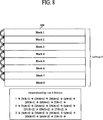
Bei einem Beispiel kann in dem Abtastmodus, wenn das Abtasten der Pixel sequenziell für eine horizontale Leitung nach der anderen durchgeführt wird, die Abtastleitung von einem Beobachter gesehen und wahrgenommen werden. Um dieses Problem zu überwinden, kann die gesamte Leitung in eine Vielzahl von Blöcke (beispielsweise vier Blöcke oder acht Blöcke) eingeteilt werden, und die unterteilten Blöcke können sequenziell oder nicht-sequenziell abgetastet werden.In one example, in the scan mode, when scanning the pixels sequentially for one horizontal line after another, the scan line may be seen and perceived by an observer. To overcome this problem, the entire line may be divided into a plurality of blocks (for example, four blocks or eight blocks), and the divided blocks may be scanned sequentially or non-sequentially.
Beispielsweise wird nach dem Abtasten der ersten horizontalen Leitung des ersten Blocks die erste horizontale Leitung des zweiten Blocks abgetastet, und dann wird die erste horizontale Leitung des dritten Blocks abgetastet, wodurch die Vielzahl der Blöcke in einer Sequenz abgetastet wird. Bei diesem Abtastverfahren können das Scansignal und das Abtastsignal an die Gateleitung (GL) und die Abtastsignalleitung (SL) von dem nicht-sequenziellen Verfahren (oder Zufallsverfahren) geliefert werden.For example, after scanning the first horizontal line of the first block, the first horizontal line of the second block is scanned, and then the first horizontal line of the third block is scanned, whereby the plurality of blocks are scanned in a sequence. In this scanning method, the scanning signal and the scanning signal can be supplied to the gate line (GL) and the scanning signal line (SL) by the non-sequential method (or random method).
Indessen kann, wenn die ”m” horizontalen Linien in jedem der Vielzahl der Blöcke ausgebildet sind, eine Abtastreihenfolge der ”m” horizontalen Linien in einem Block zufällig sein. Für den Fall des Abtastmodus können das Scansignal und das Abtastsignal an die Gateleitung (GL) und die Abtastsignalleitung (SL) durch das nicht-sequenzielle Verfahren geliefert werden.Meanwhile, when the "m" horizontal lines are formed in each of the plurality of blocks, a scanning order of the "m" horizontal lines in one block may be random. In the case of the scanning mode, the scanning signal and the scanning signal may be supplied to the gate line (GL) and the scanning signal line (SL) by the non-sequential method.
Der Gatetreiber
Der Gatetreiber
Beim Abtastmodus kann die Zeitsteuerung
Die Zeitsteuerung
Der Abtastmodus kann zu einer Initialisierungstreibezeit, einer Langzeittreibeendzeit oder eine Austastperiode eines Bildes zum Anzeigen eines Bildes auf der Anzeigetafel
Im Abtastmodus kann zu der Starttreibezeit der Anzeigetafel
Während der Vielzahl der Bilder kann der Vorgang zum Abtasten der Schwellspannung/Driftbeweglichkeit des Treibe-TFT (DT) wiederholt durchgeführt werden, wodurch die Schwellspannung/Driftbeweglichkeit des Treibe-TFT (DT) für alle Pixel (P) der Anzeigetafel
Beim Abtastmodus der Austastzeit kann die Zeitsteuerung
Gemäß dem oben beschriebenen Verfahren kann die Zeitsteuerung
Das Zeitsynchronisationssignal (TSS) kann ein vertikales Synchronisationssignal (Vsync), ein horizontales Synchronisationssignal (Hsync), ein Datenfreigabesignal (DE), ein Zeittakt (DCLK) usw. sein. Das Gatesteuersignal (GCS) kann ein Gatestartsignal und eine Vielzahl von Zeittaktsignalen umfassen. Das Datensteuersignal (DCS) kann ein Datenstartsignal, ein Datenverschiebesignal und ein Datenausgangssignal umfassen.The time synchronization signal (TSS) may be a vertical synchronization signal (Vsync), a horizontal synchronization signal (Hsync), a data enable signal (DE), a timing clock (DCLK), etc. The gate control signal (GCS) may include a gate start signal and a plurality of timing signals. The data control signal (DCS) may include a data start signal, a data shift signal, and a data output signal.
Beim Abtastmodus kann die Zeitsteuerung
Im Treibemodus kann die Zeitsteuerung
In diesem Fall können die an jeden Pixel (P) gelieferten Pixeldaten (DATA) einen Spannungspegel aufweisen, in dem sich eine Kompensationsspannung zum Kompensieren der Schwellspannung/Driftbeweglichkeit des Treibetransistors TFT (DT) für jeden Pixel (P) widerspiegelt.In this case, the pixel data (DATA) supplied to each pixel (P) may have a voltage level reflecting a compensation voltage for compensating the threshold voltage / drift mobility of the driving transistor TFT (DT) for each pixel (P).
Die Eingangsdaten (Idata) können rote, grüne und blaue Eingangsdaten umfassen, die an einen Einheitspixel geliefert werden sollen. Wenn der Einheitspixel rote, grüne und blaue Pixel umfasst, kann eine der Pixeldaten (DATA) rote, grüne oder blaue Daten sein. Indessen kann, wenn der Einheitspixel rote, grüne, blaue und weiße Pixel umfasst, eine der Pixeldaten (DATA) rote, grüne, blaue oder weiße Daten umfassen.The input data (Idata) may include red, green and blue input data to be provided to a unit pixel. If the unit pixel includes red, green and blue pixels, one of the pixel data (DATA) may be red, green or blue data. Meanwhile, when the unit pixel includes red, green, blue, and white pixels, one of the pixel data (DATA) may include red, green, blue, or white data.
Wie in der
Der Treibermodus zum Anzeigen eines Bildes kann betrieben werden, um die Datenladeperiode zum Laden jedes Pixels mit der Datenspannung und die Lichtemittierungsperiode zum Betreiben der organischen Licht emittierenden Diode (OLED) aufzuweisen. Auch kann der Abtastmodus betrieben werden, um eine Initialisierungsperiode zum Initialisieren von jedem Pixel, eine Abtastspannungsladungsperiode und eine Abtastperiode aufzuweisen.The driving mode for displaying an image may be operated to have the data charging period for charging each pixel with the data voltage and the light emitting period for operating the organic light emitting diode (OLED). Also, the scanning mode may be operated to have an initialization period for initializing each pixel, a scanning voltage charging period and a sampling period.
Der Datentreiber
Der Datenspannungserzeuger
Das Schieberegister kann ein Abfragesignal erzeugen, und der Zwischenspeicher kann die Pixeldaten (DATA) gemäß dem Abfragesignal zwischenspeichern. Der Grauwertspannungserzeuger kann eine Vielzahl von Grauwertspannungen unter Verwendung von Referenzgammaspannungen erzeugen, und der Digital-Analog-Wandler (DAC) kann die Grauwertspannung entsprechend zu dem zwischengespeicherten Pixel (DATA) unter der Vielzahl von Grauwertspannungen auswählen und die ausgewählte Grauwertspannung als die Datenspannung (Vdata) ausgeben. Dann kann das Ausgabeteil die Datenspannung (Vdata) an die Datenleitungen (DL) ausgeben.The shift register may generate an interrogation signal, and the latches may latch the pixel data (DATA) in accordance with the interrogation signal. The gray level voltage generator may generate a plurality of gray level voltages using reference gamma voltages, and the digital-to-analog converter (DAC) may select the gray level voltage corresponding to the buffered pixel (DATA) among the plurality of gray level voltages and select the selected gray level voltage as the data voltage (Vdata). output. Then, the output part can output the data voltage (Vdata) to the data lines (DL).
Der Schalter
Bei dem Treibemodus kann die Vielzahl der ersten Schalter
Im Abtastmodus können die Vielzahl von zweiten Schaltern
Wenn der Abtastdatenerzeuger
In diesem Fall kann die von der Referenzspannungsleitung (RL) abgetastete Spannung durch ein Verhältnis des an den Treibe-TFT (DT) fließenden Stroms gemäß einer Änderung der Zeit zu einer Kapazität der Referenzspannungsleitung (RL) bestimmt werden. In diesem Fall können die Abtastdaten die Daten sein, die der Schwellspannung/Driftbeweglichkeit des Treibe-TFT (DT) für jeden Pixel (P) entsprechen.In this case, the voltage sampled from the reference voltage line (RL) may be determined by a ratio of the current flowing to the driving TFT (DT) according to a change in the time to a capacitance of the reference voltage line (RL). In this case, the sampling data may be the data corresponding to the threshold voltage / drift mobility of the driving TFT (DT) for each pixel (P).
Die
In dem Treibemodus zum Anzeige eines Bildes kann ein Bild durch Liefern der Datenspannung (Vdata) gemäß den Videodaten von der ersten Datenleitung an die letzte Datenleitung für eine Zeitperiode von N Bildern angezeigt werden. In diesem Fall kann die Abtastleistungsleitung (SL) mit der Anzeigereferenzspannung (Vpre_r) versorgt werden.In the drive mode for displaying an image, an image may be displayed by supplying the data voltage (Vdata) according to the video data from the first data line to the last data line for a time period of N pictures. In this case, the sense power line (SL) can be supplied with the display reference voltage (Vpre_r).
Die Vielzahl von zweiten Schaltern
Nach dem Floaten der Referenzspannungsleitung (RL) durch den zweiten Schalter
Der Abtastdatenerzeuger
Die
Gemäß der
Um dieses Problem zu überwinden, können die 'n' horizontalen Leitungen der Anzeigetafel in eine Vielzahl von Blöcken unterteilt werden, beispielsweise in vier Blöcke, und dann können die Vielzahl der Blöcke in einer Sequenz abgetastet werden. Also können anstatt einem kontinuierlichen Abtasten der in demselben Block angeordneten horizontalen Leitungen, die horizontalen Leitungen mit verschiedenen Blöcken sequenziell oder nicht-sequenziell abgetastet werden.To overcome this problem, the 'n' horizontal lines of the display panel may be divided into a plurality of blocks, for example, four blocks, and then the plurality of blocks may be scanned in a sequence. Thus, instead of continuously scanning the horizontal lines arranged in the same block, the horizontal lines with different blocks may be scanned sequentially or non-sequentially.
Zum Beispiel kann nach dem Abtasten der ersten Abtastleitung des ersten Blocks die erste Abtastleitung des zweiten Blocks abgetastet werden. Anschließend kann die erste Abtastleitung des dritten Blocks abgetastet werden, und dann kann die erste Abtastleitung des vierten Blocks abgetastet werden.For example, after scanning the first scan line of the first block, the first scan line of the second block may be scanned. Subsequently, the first scanning line of the third block can be scanned, and then the first scanning line of the fourth block can be scanned.
Mit demselben Verfahren kann nach dem Abtasten der zweiten Abtastleitung des ersten Blocks, die zweite Abtastleitung des zweiten Blocks abgetastet werden. Danach kann nach dem Abtasten der zweiten Abtastleitung des dritten Blocks die zweite Abtastleitung des vierten Blocks abgetastet werden.With the same method, after scanning the second scanning line of the first block, the second scanning line of the second block can be scanned. Thereafter, after scanning the second scanning line of the third block, the second scanning line of the fourth block can be scanned.
Wenn die vier Blöcke nacheinander in der Reihenfolge von der ersten Abtastleitung zu der letzten Abtastleitung in jedem der vier Blöcke abgetastet werden, kann der Abtastvorgang aufgrund des Intervalls zwischen jedem der Blöcke diskontinuierlich sein. Somit ist es möglich, zu verhindern, dass die Abtastleitung des Bildschirms durch den Echtzeitabtastvorgang für die externe Kompensation wahrgenommen wird.When the four blocks are scanned one by one in the order from the first scanning line to the last scanning line in each of the four blocks, the scanning operation may be discontinuous due to the interval between each of the blocks. Thus, it is possible to prevent the scanning line of the screen from being detected by the external compensation real-time scanning operation.
Es kann unnötig sein, die Pixel in einer aufsteigenden Reihenfolge von dem ersten Block bis zu dem vierten Block abzutasten. Gemäß einem anderen Beispiel ist es möglich, die vier Blöcke nicht-sequenziell oder zufällig abzutasten.It may be unnecessary to scan the pixels in an ascending order from the first block to the fourth block. As another example, it is possible to sample the four blocks non-sequentially or randomly.
Gemäß der
Beispielsweise kann nach dem Abtasten der ersten Abtastleitung des ersten Blocks, die erste Abtastleitung des zweiten Blocks abgetastet werden. Dann kann nach dem Abtasten der ersten Abtastleitung des dritten Blocks, die erste Abtastleitung des vierten Blocks abgetastet werden. Anschließend kann nach dem Abtasten der ersten Abtastleitung des fünften Blocks, die erste Abtastleitung des sechsten Blocks abgetastet werden. Dann kann nach dem Abtasten der ersten Abtastleitung des siebten Blocks, die erste Abtastleitung des achten Blocks abgetastet werden.For example, after scanning the first scan line of the first block, the first scan line of the second block may be scanned. Then, after scanning the first scanning line of the third block, the first scanning line of the fourth block can be scanned. Subsequently, after the scanning of the first scanning line of the fifth block, the first Scanned scanning line of the sixth block. Then, after scanning the first scanning line of the seventh block, the first scanning line of the eighth block can be scanned.
Mit demselben Verfahren kann nach dem Abtasten der zweiten Abtastleitung des ersten Blocks, die zweite Abtastleitung des zweiten Blocks abgetastet werden. Dann kann nach dem Abtasten der zweiten Abtastleitung des dritten Blocks, die zweite Abtastleitung des vierten Blocks abgetastet werden. Anschließend kann nach dem Abtasten der zweiten Abtastleitung des fünften Blocks, die zweite Abtastleitung des sechsten Blocks abgetastet werden. Dann kann nach dem Abtasten der zweiten Abtastleitung des siebten Blocks, die zweite Abtastleitung des achten Blocks abgetastet werden.With the same method, after scanning the second scanning line of the first block, the second scanning line of the second block can be scanned. Then, after scanning the second scanning line of the third block, the second scanning line of the fourth block can be scanned. Subsequently, after scanning the second scanning line of the fifth block, the second scanning line of the sixth block may be scanned. Then, after scanning the second scanning line of the seventh block, the second scanning line of the eighth block can be scanned.
Wenn die acht Blöcke nacheinander in der Reihenfolge von der ersten Abtastleitung bis zur letzten Abtastleitung in jedem der acht Blöcke abgetastet werden, kann der Abtastvorgang diskontinuierlich aufgrund des Intervalls zwischen jedem der Blöcke sein. Somit ist es möglich zu verhindern, dass die Abtastleitung von dem Echtzeitabtastvorgang für die externe Kompensation wahrgenommen wird.When the eight blocks are sequentially scanned in the order from the first scanning line to the last scanning line in each of the eight blocks, the scanning operation may be discontinuous due to the interval between each of the blocks. Thus, it is possible to prevent the scanning line from being sensed by the external compensation real-time sampling process.
Es kann unnötig sein, die Pixel in einer aufsteigenden Reihenfolge von dem ersten Block bis zu dem achten Block abzutasten. Gemäß einem anderen Beispiel ist es möglich, die acht Blöcke nicht-sequenziell oder zufällig abzutasten.It may be unnecessary to scan the pixels in an ascending order from the first block to the eighth block. As another example, it is possible to sample the eight blocks non-sequentially or randomly.
Gemäß der
Beispielsweise werden die Vielzahl der Blöcke sequenziell oder nicht-sequenziell abgetastet. Wenn eine der 'm' horizontalen Leitungen, die in dem ersten Block zur Verfügung gestellt ist, in dem nicht-sequenziellen Verfahren während der ersten Bildperiode abgetastet werden kann, kann eine der 'm' horizontalen Leitungen, die in dem zweiten Block zur Verfügung gestellt ist, in dem nicht-sequenziellen Verfahren während der zweiten Bildperiode abgetastet werden.For example, the plurality of blocks are scanned sequentially or non-sequentially. If one of the 'm' horizontal lines provided in the first block can be sampled in the non-sequential process during the first frame period, one of the 'm' horizontal lines provided in the second block may be provided is sampled in the non-sequential process during the second frame period.
Anstatt dem Abtasten der horizontalen Leitungen, die in demselben Block angeordnet sind, können während aufeinanderfolgenden Bildperioden die horizontalen Leitungen, die in unterschiedlichen Blöcken zur Verfügung gestellt sind, abgetastet werden, um zu verhindern, dass die Abtastleitung durch den Echtzeitabtastvorgang wahrgenommen werden kann.Instead of scanning the horizontal lines arranged in the same block, during consecutive frame periods, the horizontal lines provided in different blocks may be scanned to prevent the scan line from being perceived by the real-time sampling process.
In diesem Fall können anstatt dem Abtasten von allen Pixeln, die in einer horizontalen Leitung bereitgestellt sind, während einem Bild die Vielzahl der Pixel, die auf einer horizontalen Leitung ausgebildet sind, während der Vielzahl der Bilder abgetastet werden.In this case, instead of scanning all the pixels provided in a horizontal line during one picture, the plurality of pixels formed on a horizontal line may be scanned during the plurality of pictures.
Wie in der
Wenn die Vielzahl der Pixel, die in einer horizontalen Leitung ausgebildet sind, unter der Vielzahl von Bildern verteilt werden und während diese abgetastet werden, ist es möglich, zu verhindern, dass die Datenleitung durch den Echtzeitabtastvorgang gesehen und wahrgenommen wird, aber Ausführungsformen sind nicht auf das Obige beschränkt. Wenn die Vielzahl der Pixel, die in einer horizontalen Leitung ausgebildet sind, unter der Vielzahl von Bildern verteilt werden und während diesen abgetastet werden, ist die Anzahl von Bildern nicht beschränkt, also kann die Anzahl der Bilder in Anbetracht der Eigenschaften der Anzeigetafel und der Abtastzeit nach Ermessen bestimmt werden.When the plurality of pixels formed in a horizontal line are distributed among the plurality of pictures and while they are being scanned, it is possible to prevent the data line from being seen and perceived by the real-time sampling, but embodiments are not the above is limited. When the plurality of pixels formed in a horizontal line are distributed among and scanned among the plurality of images, the number of images is not limited, so the number of images may be in consideration of the characteristics of the display panel and the sampling time be determined at its discretion.
Somit kann die Schwellspannung/Driftmobilität des Treibe-TFT (DT) für alle Pixel der Anzeigetafel alle durch die Austastperioden des Bildes erfasst werden, und dann kann die Datenspannung (Vdata), die an die Pixel (P) angelegt wird, durch die Verwendung der Kompensationsdaten basierend auf der erfassten Schwellspannung/Driftmobilität kompensiert werden. Somit kann die externe Kompensation mit hoher Effizienz ohne einem Sichtbarwerden der Abtastleitung durchgeführt werden, wodurch verhindert wird, dass eine Bildqualität durch den Echtzeitabtastvorgang für die externe Kompensation verschlechtert wird.Thus, the threshold voltage / drift mobility of the driving TFT (DT) for all the pixels of the display panel can all be detected by the blanking periods of the image, and then the data voltage (Vdata) applied to the pixels (P) can be obtained by using the Compensation data based on the detected threshold voltage / drift mobility can be compensated. Thus, the external compensation can be performed with high efficiency without the visibility of the scan line, thereby preventing image quality from being degraded by the real-time external compensation scan.
Gemäß dem Verfahren zum Treiben der organischen Licht emittierenden Anzeigevorrichtung der Ausführungsformen ist es möglich, zu verhindern, dass die Abtastleitung durch den Echtzeitabtastvorgang für die externe Kompensation wahrgenommen oder unterscheidbar wird, und somit wird verhindert, dass die Bildqualität sich verschlechtert, wenn der Echtzeitabtastvorgang für die externe Kompensation durchgeführt wird, wodurch eine hohe Treibezuverlässigkeit der Anzeigetafel erzeugt wird.According to the method of driving the organic light emitting display device of the embodiments, it is possible to prevent the scanning line from being perceived or discriminated by the external compensation real time sampling operation, and thus the image quality is prevented from deteriorating when the real time sampling operation for the external compensation is performed, whereby a high drive reliability of the display panel is generated.
Es wird dem Fachmann offenkundig, dass verschiedene Modifizierungen und Variationen bei den Ausführungsformen durchgeführt werden können, ohne von dem Geist und Schutzumfang der Erfindung abzuweichen. Somit ist es gedacht, dass die vorliegende Erfindung die Modifizierungen und Variationen der Erfindung umfasst, solange sie innerhalb des Schutzumfangs der anhängenden Ansprüche sowie deren Äquivalente liegt.It will be apparent to those skilled in the art that various modifications and variations can be made in the embodiments without departing from the spirit and scope of the invention. Thus, it is intended that the present invention covers the modifications and variations of the invention provided they come within the scope of the appended claims and their equivalents.
ZITATE ENTHALTEN IN DER BESCHREIBUNG QUOTES INCLUDE IN THE DESCRIPTION
Diese Liste der vom Anmelder aufgeführten Dokumente wurde automatisiert erzeugt und ist ausschließlich zur besseren Information des Lesers aufgenommen. Die Liste ist nicht Bestandteil der deutschen Patent- bzw. Gebrauchsmusteranmeldung. Das DPMA übernimmt keinerlei Haftung für etwaige Fehler oder Auslassungen.This list of the documents listed by the applicant has been generated automatically and is included solely for the better information of the reader. The list is not part of the German patent or utility model application. The DPMA assumes no liability for any errors or omissions.
Zitierte PatentliteraturCited patent literature
- KR 10-2012-0149827 [0001] KR 10-2012-0149827 [0001]
Claims (14)
Applications Claiming Priority (2)
| Application Number | Priority Date | Filing Date | Title |
|---|---|---|---|
| KR10-2012-0149827 | 2012-12-20 | ||
| KR1020120149827A KR101969436B1 (en) | 2012-12-20 | 2012-12-20 | Driving method for organic light emitting display |
Publications (2)
| Publication Number | Publication Date |
|---|---|
| DE102013112721A1 true DE102013112721A1 (en) | 2014-06-26 |
| DE102013112721B4 DE102013112721B4 (en) | 2021-03-25 |
Family
ID=50878850
Family Applications (1)
| Application Number | Title | Priority Date | Filing Date |
|---|---|---|---|
| DE102013112721.5A Active DE102013112721B4 (en) | 2012-12-20 | 2013-11-19 | A method of driving an organic light emitting display device |
Country Status (5)
| Country | Link |
|---|---|
| US (2) | US9805642B2 (en) |
| KR (1) | KR101969436B1 (en) |
| CN (1) | CN103886830B (en) |
| DE (1) | DE102013112721B4 (en) |
| TW (1) | TWI530929B (en) |
Cited By (1)
| Publication number | Priority date | Publication date | Assignee | Title |
|---|---|---|---|---|
| DE102017111958B4 (en) | 2016-05-31 | 2023-12-28 | Lg Display Co., Ltd. | ORGANIC LED DISPLAY AND METHOD FOR OPERATING THE SAME |
Families Citing this family (54)
| Publication number | Priority date | Publication date | Assignee | Title |
|---|---|---|---|---|
| KR20140066830A (en) * | 2012-11-22 | 2014-06-02 | 엘지디스플레이 주식회사 | Organic light emitting display device |
| KR102159390B1 (en) * | 2013-11-13 | 2020-09-24 | 삼성디스플레이 주식회사 | Organic light emitting display device and driving method thereof |
| KR102164157B1 (en) * | 2014-07-07 | 2020-10-13 | 엘지디스플레이 주식회사 | Display device |
| KR102122542B1 (en) * | 2014-07-10 | 2020-06-29 | 엘지디스플레이 주식회사 | Organic Light Emitting Display Device |
| KR102192522B1 (en) * | 2014-08-06 | 2020-12-18 | 엘지디스플레이 주식회사 | Organic light emitting display device |
| KR102160815B1 (en) * | 2014-09-01 | 2020-09-29 | 엘지디스플레이 주식회사 | Display device |
| KR102274740B1 (en) * | 2014-10-13 | 2021-07-08 | 삼성디스플레이 주식회사 | Display device |
| KR102229393B1 (en) * | 2014-10-13 | 2021-03-18 | 엘지디스플레이 주식회사 | Organic light emitting diode display device |
| KR102237026B1 (en) * | 2014-11-05 | 2021-04-06 | 주식회사 실리콘웍스 | Display device |
| KR102313360B1 (en) | 2014-11-10 | 2021-10-18 | 삼성디스플레이 주식회사 | Organic Light Emitting Display Device and Driving Method Thereof |
| KR102388912B1 (en) * | 2014-12-29 | 2022-04-21 | 엘지디스플레이 주식회사 | Organic light emitting diode display and drving method thereof |
| KR102377119B1 (en) * | 2014-12-30 | 2022-03-22 | 엘지디스플레이 주식회사 | Display device |
| KR101789602B1 (en) * | 2014-12-31 | 2017-10-26 | 엘지디스플레이 주식회사 | Organic light emitting display device and method for driving thereof |
| CN105023539B (en) * | 2015-07-10 | 2017-11-28 | 北京大学深圳研究生院 | Offset peripheral system, method and the display system of a kind of picture element matrix |
| KR102324660B1 (en) * | 2015-07-16 | 2021-11-10 | 엘지디스플레이 주식회사 | Method For Sensing Threshold Voltage Of Driving TFT included in Organic Light Emitting Display |
| CN105243996B (en) * | 2015-11-09 | 2018-01-30 | 深圳市华星光电技术有限公司 | Using the AMOLED drive circuit structures of external compensation |
| KR102630078B1 (en) * | 2015-12-30 | 2024-01-26 | 엘지디스플레이 주식회사 | Pixel, display device comprising the sme and driving method thereof |
| KR102576937B1 (en) * | 2015-12-31 | 2023-09-11 | 엘지디스플레이 주식회사 | Organic Light Emitting Diode display apparatus and method for performing off-real time sensing thereof |
| KR102470373B1 (en) * | 2016-04-15 | 2022-11-23 | 엘지디스플레이 주식회사 | Organic light emitting display device |
| KR102554493B1 (en) * | 2016-06-14 | 2023-07-13 | 주식회사 엘엑스세미콘 | Source driver and panel driving system |
| CN105913801B (en) * | 2016-06-20 | 2018-08-07 | 上海天马有机发光显示技术有限公司 | A kind of organic light emitting display panel and its driving method |
| KR102577493B1 (en) * | 2016-07-29 | 2023-09-11 | 엘지디스플레이 주식회사 | Organic light emitting device and its driving method |
| KR102522478B1 (en) * | 2016-11-25 | 2023-04-17 | 엘지디스플레이 주식회사 | Organic light emitting display device and method for drving the same |
| KR102617966B1 (en) * | 2016-12-28 | 2023-12-28 | 엘지디스플레이 주식회사 | Electroluminescent Display Device and Driving Method thereof |
| CN106652907B (en) * | 2017-01-05 | 2019-02-05 | 上海天马有机发光显示技术有限公司 | Organic light-emitting display panel, organic light-emitting display device and pixel compensation method |
| CN107068053B (en) * | 2017-02-21 | 2019-07-09 | 京东方科技集团股份有限公司 | Compensation data method and compensation device, the display device of OLED display |
| CN106920516B (en) * | 2017-05-12 | 2019-04-05 | 京东方科技集团股份有限公司 | Compensation method and device for OLED, display device |
| KR102316564B1 (en) * | 2017-05-29 | 2021-10-25 | 엘지디스플레이 주식회사 | OLED display device and compensation data processing method thereof |
| KR102503174B1 (en) * | 2017-07-27 | 2023-02-27 | 삼성디스플레이 주식회사 | Fingerprint sensor, display device including the same, and method for operating the fingerprint sensor |
| KR102420998B1 (en) * | 2017-08-04 | 2022-07-13 | 엘지디스플레이 주식회사 | Communication method and display device using the same |
| US10643543B2 (en) * | 2017-11-23 | 2020-05-05 | Novatek Microelectronics Corp. | Multi-sensing channels design for pixel compensation |
| US10818785B2 (en) * | 2017-12-04 | 2020-10-27 | Ecole Polytechnique Federale De Lausanne (Epfl) | Sensing device for sensing minor charge variations |
| US10762843B2 (en) * | 2018-03-28 | 2020-09-01 | Sharp Kabushiki Kaisha | Pixel circuit using direct charging and that performs light-emitting device compensation |
| CN108806567B (en) * | 2018-07-02 | 2021-03-23 | 京东方科技集团股份有限公司 | Display panel, detection method and detection module thereof, and display device |
| KR102582823B1 (en) * | 2018-07-05 | 2023-09-27 | 삼성디스플레이 주식회사 | Organic light emitting display device and method of driving the same |
| CN109935185B (en) * | 2018-07-18 | 2022-07-01 | 京东方科技集团股份有限公司 | Shifting register unit and driving method thereof, grid driving circuit and display device |
| US11361710B2 (en) | 2018-09-20 | 2022-06-14 | Boe Technology Group Co., Ltd. | Pixel circuit with a time-shared signal line, a pixel compensation method, and a display apparatus |
| KR102818264B1 (en) | 2018-10-08 | 2025-06-11 | 삼성디스플레이 주식회사 | Gate driver and display device including the gate driver |
| WO2020073227A1 (en) * | 2018-10-10 | 2020-04-16 | 深圳市柔宇科技有限公司 | Externally electrically compensated pixel circuit, drive method, and display screen |
| KR102589012B1 (en) * | 2018-11-06 | 2023-10-16 | 삼성디스플레이 주식회사 | Method of performing a sensing operation in an organic light emitting display device, and organic light emitting display device |
| CN109584801A (en) * | 2018-12-14 | 2019-04-05 | 云谷(固安)科技有限公司 | Pixel circuit, display panel, display device and driving method |
| KR102710287B1 (en) * | 2018-12-20 | 2024-09-25 | 엘지디스플레이 주식회사 | Electroluminescence display device including gate driver |
| KR20190016521A (en) | 2019-01-29 | 2019-02-18 | 이태자 | Deviate prevention and dust collecting device capable of removing the belt deviation of the conveyor device and dust attached to the belt surface |
| US11062648B2 (en) * | 2019-05-13 | 2021-07-13 | Novatek Microelectronics Corp. | Display device and method of sensing the same |
| US11107410B2 (en) * | 2019-08-15 | 2021-08-31 | Hefei Boe Joint Technology Co., Ltd. | Pixel circuit and method of controlling the same, display panel and display device |
| KR102709912B1 (en) * | 2019-11-14 | 2024-09-27 | 삼성디스플레이 주식회사 | Display device and driving method thereof |
| CN110930913B (en) * | 2019-12-10 | 2021-10-22 | 京东方科技集团股份有限公司 | Display compensation data, data detection method and device thereof, and display panel |
| CN111063302A (en) * | 2019-12-17 | 2020-04-24 | 深圳市华星光电半导体显示技术有限公司 | Pixel hybrid compensation circuit and pixel hybrid compensation method |
| CN111883062B (en) * | 2020-06-29 | 2021-10-22 | 北京大学深圳研究生院 | Compensation driving method, driving device and display device for pixel array |
| US11874997B2 (en) * | 2020-11-27 | 2024-01-16 | Sharp Kabushiki Kaisha | Display device equipped with touch panel and control method therefor |
| KR102899771B1 (en) * | 2021-04-30 | 2025-12-12 | 엘지디스플레이 주식회사 | Light Emitting Display Device and Driving Method of the same |
| US12073792B2 (en) * | 2021-05-26 | 2024-08-27 | Boe Technology Group Co., Ltd. | Data driving integrated circuit, display apparatus, and pixel compensation method |
| US12118906B2 (en) | 2021-05-28 | 2024-10-15 | Hefei Boe Joint Technology Co., Ltd. | Method for sensing display panel, and display panel |
| KR102764588B1 (en) | 2021-12-30 | 2025-02-07 | 엘지디스플레이 주식회사 | Gate driver and display device using the same |
Family Cites Families (27)
| Publication number | Priority date | Publication date | Assignee | Title |
|---|---|---|---|---|
| US5534892A (en) * | 1992-05-20 | 1996-07-09 | Sharp Kabushiki Kaisha | Display-integrated type tablet device having and idle time in one display image frame to detect coordinates and having different electrode densities |
| TW544650B (en) * | 2000-12-27 | 2003-08-01 | Matsushita Electric Industrial Co Ltd | Matrix-type display device and driving method thereof |
| EP1640958A2 (en) * | 2004-09-27 | 2006-03-29 | Idc, Llc | System with server based control of client device display features |
| US7907137B2 (en) * | 2005-03-31 | 2011-03-15 | Casio Computer Co., Ltd. | Display drive apparatus, display apparatus and drive control method thereof |
| CN104965621B (en) * | 2006-06-09 | 2018-06-12 | 苹果公司 | Touch screen LCD and its operating method |
| US8552989B2 (en) * | 2006-06-09 | 2013-10-08 | Apple Inc. | Integrated display and touch screen |
| KR100898675B1 (en) * | 2007-04-19 | 2009-05-22 | 삼성모바일디스플레이주식회사 | Organic electroluminescent display, multifunction keypad display using same and driving method thereof |
| KR100932205B1 (en) | 2008-03-31 | 2009-12-16 | 한양대학교 산학협력단 | A pixel circuit, a display device including the same, and a method of operating the pixel circuit |
| US8405582B2 (en) * | 2008-06-11 | 2013-03-26 | Samsung Display Co., Ltd. | Organic light emitting display and driving method thereof |
| KR20100034560A (en) * | 2008-09-24 | 2010-04-01 | 삼성전자주식회사 | Display device and driving method thereof |
| KR101329458B1 (en) * | 2008-10-07 | 2013-11-15 | 엘지디스플레이 주식회사 | Organic Light Emitting Diode Display |
| JP5456372B2 (en) | 2009-05-29 | 2014-03-26 | グローバル・オーエルイーディー・テクノロジー・リミテッド・ライアビリティ・カンパニー | Display device |
| KR101073297B1 (en) * | 2009-07-10 | 2011-10-12 | 삼성모바일디스플레이주식회사 | Organic Light Emitting Display and Driving Method Thereof |
| JP5275956B2 (en) | 2009-10-15 | 2013-08-28 | 株式会社ジャパンディスプレイウェスト | Information input device, information input program, and electronic device |
| KR101388286B1 (en) * | 2009-11-24 | 2014-04-22 | 엘지디스플레이 주식회사 | Organic Light Emitting Diode Display And Driving Method Thereof |
| US8542202B2 (en) * | 2009-12-31 | 2013-09-24 | Motorola Mobility Llc | Electronic device and method for determining a touch input applied to a capacitive touch panel system incorporated therein |
| KR101201722B1 (en) * | 2010-02-23 | 2012-11-15 | 삼성디스플레이 주식회사 | Organic light emitting display and driving method thereof |
| KR101065405B1 (en) | 2010-04-14 | 2011-09-16 | 삼성모바일디스플레이주식회사 | Display device and driving method |
| KR101097353B1 (en) * | 2010-05-07 | 2011-12-23 | 삼성모바일디스플레이주식회사 | A gate driving circuit and a organic electroluminescent display apparatus using the same |
| KR101223488B1 (en) | 2010-05-11 | 2013-01-17 | 삼성디스플레이 주식회사 | Organic Light Emitting Display and Driving Method Thereof |
| KR20110133281A (en) * | 2010-06-04 | 2011-12-12 | 삼성모바일디스플레이주식회사 | OLED display and driving method thereof |
| JP5722573B2 (en) * | 2010-08-24 | 2015-05-20 | 株式会社ジャパンディスプレイ | Display device with touch detection function |
| KR101761580B1 (en) * | 2010-09-08 | 2017-07-27 | 엘지디스플레이 주식회사 | Display device having touch sensor |
| CN103168324B (en) * | 2010-10-21 | 2015-08-05 | 夏普株式会社 | Display device and driving method thereof |
| US8804056B2 (en) * | 2010-12-22 | 2014-08-12 | Apple Inc. | Integrated touch screens |
| KR102040843B1 (en) * | 2011-01-04 | 2019-11-06 | 삼성디스플레이 주식회사 | Organic light emitting display and driving method thereof |
| KR101648571B1 (en) * | 2014-07-16 | 2016-08-18 | 엘지디스플레이 주식회사 | In-cell touch type display device |
-
2012
- 2012-12-20 KR KR1020120149827A patent/KR101969436B1/en active Active
-
2013
- 2013-11-19 DE DE102013112721.5A patent/DE102013112721B4/en active Active
- 2013-12-04 TW TW102144462A patent/TWI530929B/en active
- 2013-12-09 CN CN201310661411.0A patent/CN103886830B/en active Active
- 2013-12-17 US US14/108,356 patent/US9805642B2/en active Active
-
2017
- 2017-09-27 US US15/717,146 patent/US10896637B2/en active Active
Cited By (1)
| Publication number | Priority date | Publication date | Assignee | Title |
|---|---|---|---|---|
| DE102017111958B4 (en) | 2016-05-31 | 2023-12-28 | Lg Display Co., Ltd. | ORGANIC LED DISPLAY AND METHOD FOR OPERATING THE SAME |
Also Published As
| Publication number | Publication date |
|---|---|
| KR20140080243A (en) | 2014-06-30 |
| US20180018915A1 (en) | 2018-01-18 |
| US10896637B2 (en) | 2021-01-19 |
| TWI530929B (en) | 2016-04-21 |
| US20140176401A1 (en) | 2014-06-26 |
| US9805642B2 (en) | 2017-10-31 |
| KR101969436B1 (en) | 2019-04-16 |
| DE102013112721B4 (en) | 2021-03-25 |
| CN103886830A (en) | 2014-06-25 |
| CN103886830B (en) | 2016-08-24 |
| TW201426703A (en) | 2014-07-01 |
Similar Documents
| Publication | Publication Date | Title |
|---|---|---|
| DE102013112721B4 (en) | A method of driving an organic light emitting display device | |
| DE102020115386B4 (en) | Display device and control method therefor | |
| DE102020125417B4 (en) | DISPLAY DEVICE AND METHOD FOR CONTROLLING THE SAME | |
| DE102013110995B4 (en) | An organic light emitting display device and method for operating the same | |
| DE102010061736B4 (en) | Organic light-emitting diode display device and method for driving the same | |
| DE102015107326B4 (en) | Organic light-emitting diode display device and driving method therefor | |
| DE102020132136A1 (en) | Pixel drive circuit and electroluminescent display device containing it | |
| DE102006054510B4 (en) | Display with organic light-emitting diodes and method for its control | |
| DE102021131610A1 (en) | ORGANIC LIGHT EMITTING DISPLAY DEVICE | |
| DE102020120794A1 (en) | DISPLAY DEVICE AND CONTROL METHODS OF THE SAME | |
| DE102014118997A1 (en) | Organic light-emitting display device and method for driving the same | |
| DE102017128819A1 (en) | DISPLAY FIELD AND ELECTROLUMINESCENCE DISPLAY USING THEREOF | |
| DE102020103876A1 (en) | Display drive circuit and display device with the same | |
| DE102018217781A1 (en) | Pixel switching, display and method | |
| DE102016125941A1 (en) | Organic self-luminous display device and method for compensating the image quality of the organic self-luminous display device | |
| DE102017122687A1 (en) | Light-emitting display device and method for its control | |
| DE102019121211A1 (en) | Data driver circuit, control unit, display device and method for controlling it | |
| DE102021133258A1 (en) | display device | |
| DE102018219989A1 (en) | Pixel switching, display and method | |
| DE102019131961A1 (en) | PIXEL DETECTING DEVICE AND METHOD, DATA DRIVER AND ORGANIC LIGHT-EMITTING DISPLAY DEVICE | |
| DE102021133244A1 (en) | Gate drive circuit and electroluminescence display device using it | |
| DE102012112534A1 (en) | Light-emitting display device | |
| DE102020127610A1 (en) | LIGHT EMITTING DISPLAY DEVICE AND METHOD FOR CONTROLLING THE SAME | |
| DE102017130539A1 (en) | ORGANIC LIGHT EMITTING DISPLAY PANEL AND ORGANIC LIGHT EMITTING DISPLAY DEVICE WITH THE SAME | |
| DE102017125320A1 (en) | Data driver and display device using it |
Legal Events
| Date | Code | Title | Description |
|---|---|---|---|
| R012 | Request for examination validly filed | ||
| R016 | Response to examination communication | ||
| R018 | Grant decision by examination section/examining division | ||
| R020 | Patent grant now final |