DE102013103057A1 - Device for FinFETs - Google Patents
Device for FinFETs Download PDFInfo
- Publication number
- DE102013103057A1 DE102013103057A1 DE102013103057A DE102013103057A DE102013103057A1 DE 102013103057 A1 DE102013103057 A1 DE 102013103057A1 DE 102013103057 A DE102013103057 A DE 102013103057A DE 102013103057 A DE102013103057 A DE 102013103057A DE 102013103057 A1 DE102013103057 A1 DE 102013103057A1
- Authority
- DE
- Germany
- Prior art keywords
- fin
- stage
- drain
- channel
- source region
- Prior art date
- Legal status (The legal status is an assumption and is not a legal conclusion. Google has not performed a legal analysis and makes no representation as to the accuracy of the status listed.)
- Granted
Links
Images


Classifications
-
- H—ELECTRICITY
- H10—SEMICONDUCTOR DEVICES; ELECTRIC SOLID-STATE DEVICES NOT OTHERWISE PROVIDED FOR
- H10B—ELECTRONIC MEMORY DEVICES
- H10B10/00—Static random access memory [SRAM] devices
- H10B10/12—Static random access memory [SRAM] devices comprising a MOSFET load element
-
- H—ELECTRICITY
- H10—SEMICONDUCTOR DEVICES; ELECTRIC SOLID-STATE DEVICES NOT OTHERWISE PROVIDED FOR
- H10D—INORGANIC ELECTRIC SEMICONDUCTOR DEVICES
- H10D30/00—Field-effect transistors [FET]
- H10D30/01—Manufacture or treatment
- H10D30/021—Manufacture or treatment of FETs having insulated gates [IGFET]
- H10D30/024—Manufacture or treatment of FETs having insulated gates [IGFET] of fin field-effect transistors [FinFET]
- H10D30/0245—Manufacture or treatment of FETs having insulated gates [IGFET] of fin field-effect transistors [FinFET] by further thinning the channel after patterning the channel, e.g. using sacrificial oxidation on fins
-
- H—ELECTRICITY
- H10—SEMICONDUCTOR DEVICES; ELECTRIC SOLID-STATE DEVICES NOT OTHERWISE PROVIDED FOR
- H10D—INORGANIC ELECTRIC SEMICONDUCTOR DEVICES
- H10D30/00—Field-effect transistors [FET]
- H10D30/60—Insulated-gate field-effect transistors [IGFET]
- H10D30/62—Fin field-effect transistors [FinFET]
- H10D30/6212—Fin field-effect transistors [FinFET] having fin-shaped semiconductor bodies having non-rectangular cross-sections
-
- H—ELECTRICITY
- H10—SEMICONDUCTOR DEVICES; ELECTRIC SOLID-STATE DEVICES NOT OTHERWISE PROVIDED FOR
- H10D—INORGANIC ELECTRIC SEMICONDUCTOR DEVICES
- H10D84/00—Integrated devices formed in or on semiconductor substrates that comprise only semiconducting layers, e.g. on Si wafers or on GaAs-on-Si wafers
- H10D84/01—Manufacture or treatment
- H10D84/0123—Integrating together multiple components covered by H10D12/00 or H10D30/00, e.g. integrating multiple IGBTs
- H10D84/0126—Integrating together multiple components covered by H10D12/00 or H10D30/00, e.g. integrating multiple IGBTs the components including insulated gates, e.g. IGFETs
- H10D84/0158—Integrating together multiple components covered by H10D12/00 or H10D30/00, e.g. integrating multiple IGBTs the components including insulated gates, e.g. IGFETs the components including FinFETs
-
- H—ELECTRICITY
- H10—SEMICONDUCTOR DEVICES; ELECTRIC SOLID-STATE DEVICES NOT OTHERWISE PROVIDED FOR
- H10D—INORGANIC ELECTRIC SEMICONDUCTOR DEVICES
- H10D84/00—Integrated devices formed in or on semiconductor substrates that comprise only semiconducting layers, e.g. on Si wafers or on GaAs-on-Si wafers
- H10D84/01—Manufacture or treatment
- H10D84/02—Manufacture or treatment characterised by using material-based technologies
- H10D84/03—Manufacture or treatment characterised by using material-based technologies using Group IV technology, e.g. silicon technology or silicon-carbide [SiC] technology
- H10D84/038—Manufacture or treatment characterised by using material-based technologies using Group IV technology, e.g. silicon technology or silicon-carbide [SiC] technology using silicon technology, e.g. SiGe
-
- H—ELECTRICITY
- H10—SEMICONDUCTOR DEVICES; ELECTRIC SOLID-STATE DEVICES NOT OTHERWISE PROVIDED FOR
- H10D—INORGANIC ELECTRIC SEMICONDUCTOR DEVICES
- H10D84/00—Integrated devices formed in or on semiconductor substrates that comprise only semiconducting layers, e.g. on Si wafers or on GaAs-on-Si wafers
- H10D84/80—Integrated devices formed in or on semiconductor substrates that comprise only semiconducting layers, e.g. on Si wafers or on GaAs-on-Si wafers characterised by the integration of at least one component covered by groups H10D12/00 or H10D30/00, e.g. integration of IGFETs
- H10D84/82—Integrated devices formed in or on semiconductor substrates that comprise only semiconducting layers, e.g. on Si wafers or on GaAs-on-Si wafers characterised by the integration of at least one component covered by groups H10D12/00 or H10D30/00, e.g. integration of IGFETs of only field-effect components
- H10D84/83—Integrated devices formed in or on semiconductor substrates that comprise only semiconducting layers, e.g. on Si wafers or on GaAs-on-Si wafers characterised by the integration of at least one component covered by groups H10D12/00 or H10D30/00, e.g. integration of IGFETs of only field-effect components of only insulated-gate FETs [IGFET]
- H10D84/85—Complementary IGFETs, e.g. CMOS
- H10D84/853—Complementary IGFETs, e.g. CMOS comprising FinFETs
-
- H—ELECTRICITY
- H10—SEMICONDUCTOR DEVICES; ELECTRIC SOLID-STATE DEVICES NOT OTHERWISE PROVIDED FOR
- H10W—GENERIC PACKAGES, INTERCONNECTIONS, CONNECTORS OR OTHER CONSTRUCTIONAL DETAILS OF DEVICES COVERED BY CLASS H10
- H10W10/00—Isolation regions in semiconductor bodies between components of integrated devices
- H10W10/01—Manufacture or treatment
- H10W10/011—Manufacture or treatment of isolation regions comprising dielectric materials
- H10W10/014—Manufacture or treatment of isolation regions comprising dielectric materials using trench refilling with dielectric materials, e.g. shallow trench isolations
- H10W10/0145—Manufacture or treatment of isolation regions comprising dielectric materials using trench refilling with dielectric materials, e.g. shallow trench isolations of trenches having shapes other than rectangular or V-shape
-
- H—ELECTRICITY
- H10—SEMICONDUCTOR DEVICES; ELECTRIC SOLID-STATE DEVICES NOT OTHERWISE PROVIDED FOR
- H10W—GENERIC PACKAGES, INTERCONNECTIONS, CONNECTORS OR OTHER CONSTRUCTIONAL DETAILS OF DEVICES COVERED BY CLASS H10
- H10W10/00—Isolation regions in semiconductor bodies between components of integrated devices
- H10W10/10—Isolation regions comprising dielectric materials
- H10W10/17—Isolation regions comprising dielectric materials formed using trench refilling with dielectric materials, e.g. shallow trench isolations
Landscapes
- Metal-Oxide And Bipolar Metal-Oxide Semiconductor Integrated Circuits (AREA)
- Thin Film Transistor (AREA)
- Insulated Gate Type Field-Effect Transistor (AREA)
- Semiconductor Memories (AREA)
Abstract
Ein FinFET umfasst ein Isolationsgebiet, welches in einem Substrat gebildet ist, eine umgekehrt T-förmige Finne, welche in dem Substrat gebildet ist, wobei ein unterer Bereich der umgekehrt T-förmigen Finne von dem Isolationsgebiet eingeschlossen ist und ein oberer Bereich der umgekehrt T-förmigen Finne über eine obere Fläche des Isolationsgebiets hervorsteht. Der FinFET umfasst weiter eine Gate-Elektrode, welche die umgekehrt T-förmige Finne einhüllt.A FinFET comprises an isolation region formed in a substrate, an inverted T-shaped fin formed in the substrate, a lower region of the inverted T-shaped fin being enclosed by the isolation region, and an upper region of the inverted T- shaped fin protrudes over an upper surface of the isolation area. The FinFET further includes a gate electrode which envelops the inverted T-shaped fin.
Description
Einrichtung für FinFETsDevice for FinFETs
Hintergrundbackground
Die Halbleiterindustrie hat aufgrund kontinuierlicher Verbesserungen bei der Integrationsdichte verschiedener elektronischer Komponenten (z. B. Transistoren, Dioden, Widerständen, Kondensatoren, etc.) ein schnelles Wachstum erfahren. Zum großen Teil rührt diese Verbesserung bei der Integrationsdichte von wiederholten Reduzierungen bei der minimalen Größe von Merkmalen her, wodurch mehr Komponenten auf eine gegebene Fläche integriert werden können. Allerdings kann die verringerte Merkmalsgröße zu einem größeren Leckstrom führen. Während die Nachfrage nach immer kleineren elektronischen Vorrichtungen in letzter Zeit zugenommen hat, nahm das Bedürfnis nach dem Reduzieren des Leckstroms von Halbleitervorrichtungen zu.The semiconductor industry has experienced rapid growth due to continuous improvements in the integration density of various electronic components (eg, transistors, diodes, resistors, capacitors, etc.). To a large extent, this improvement is due to the integration density of repeated reductions in the minimum feature size, allowing more components to be integrated into a given area. However, the reduced feature size may result in a larger leakage current. As the demand for smaller and smaller electronic devices has recently increased, the need for reducing the leakage current of semiconductor devices has increased.
In einem komplementären Metalloxidhalbleiter-(complementary metal Oxide semiconductor – CMOS)-Feldeffekttransistor (FET) umfassen aktive Gebiete ein Drain, ein Source, ein Kanalgebiet, welches zwischen das Drain und das Source verbunden ist, und ein Gate auf dem Kanal, um den An- und Aus-Zustand des Kanalgebiets zu steuern. Wenn die Gate-Spannung größer als eine Schwellspannung ist, wird ein leitfähiger Kanal zwischen dem Drain und dem Source hergestellt. Im Ergebnis wird es ermöglicht, dass sich Elektronen oder Löcher zwischen dem Drain und dem Source bewegen. Andererseits ist der Kanal, wenn die Gate-Spannung kleiner als die Schwellspannung ist, im Idealfall abgeschnitten und es fließen keine Elektronen oder Löcher zwischen dem Drain und dem Source. Wenn die Halbleitervorrichtungen allerdings weiter schrumpfen, kann das Gate aufgrund des Kurzkanal-Leckeffekts das Kanalgebiet, insbesondere den Bereich des Kanalgebiets, welcher weit entfernt von dem Gate ist, nicht vollständig steuern. Nachdem Halbleitervorrichtungen in tiefe Sub-30-Nanometer-Dimensionen skaliert sind, kann die entsprechende kurze Kanallänge konventioneller planarer Transistoren in der Konsequenz zu einem Unvermögen des Gates führen, das Kanalgebiet im Wesentlichen auszuschalten.In a complementary metal oxide semiconductor (CMOS) field effect transistor (FET), active regions include a drain, a source, a channel region connected between the drain and the source, and a gate on the channel around the anode and the off state of the channel region. When the gate voltage is greater than a threshold voltage, a conductive channel is established between the drain and the source. As a result, electrons or holes are allowed to move between the drain and the source. On the other hand, if the gate voltage is less than the threshold voltage, the channel is ideally cut off and no electrons or holes flow between the drain and the source. However, as semiconductor devices continue to shrink, due to the short channel leakage effect, the gate can not fully control the channel region, particularly the region of the channel region that is far from the gate. As a result, after semiconductor devices are scaled to sub-30 nanometer deep depths, the corresponding short channel length of conventional planar transistors can result in the gate becoming unable to substantially turn off the channel region.
Während sich die Halbleitertechnologien weiterentwickeln, sind Finnen-Feldeffekttransistoren (fin field effect transistors – FinFETs) als eine effektive Alternative für ein weiteres Reduzieren des Leckstroms in Halbleitervorrichtungen hervorgetreten. In einem FinFET steht ein aktives Gebiet einschließlich dem Drain, dem Kanalgebiet und dem Source von der Oberfläche des Halbleitersubstrats, auf welchem sich der FinFET befindet, hervor. Das aktive Gebiet des FinFET, wie beispielsweise eine Finne, ist in einer Querschnittsansicht von rechteckiger Form. Zusätzlich hüllt die Gate-Struktur des FinFETs das aktive Gebiet auf drei Seiten wie ein auf den Kopf gestelltes U ein. Im Ergebnis wurde die Steuerung des Kanals durch die Gate-Struktur stärker. Der Kurzkanal-Leckeffekt konventioneller planarer Transistoren wurde verringert. Tatsächlich kann die Gate-Struktur, wenn der FinFET ausgeschaltet ist, den Kanal besser steuern, um den Leckstrom zu verringern.As semiconductor technologies evolve, fin field effect transistors (FinFETs) have emerged as an effective alternative for further reducing the leakage current in semiconductor devices. In a FinFET, an active region including the drain, the channel region, and the source protrudes from the surface of the semiconductor substrate on which the FinFET is located. The active region of the FinFET, such as a fin, is rectangular in cross-sectional view. In addition, the gate structure of the FinFET wraps the active area on three sides like an upside down U. As a result, the control of the channel by the gate structure became stronger. The short-channel leakage effect of conventional planar transistors has been reduced. In fact, with the FinFET turned off, the gate structure can better control the channel to reduce the leakage current.
Kurze Beschreibung der ZeichnungenBrief description of the drawings
Für ein vollständigeres Verständnis der vorliegenden Offenbarung und deren Vorteilen wird nun auf die folgenden Beschreibungen zusammen mit den beigefügten Zeichnungen Bezug genommen, in welchen:For a more complete understanding of the present disclosure and its advantages, reference is now made to the following descriptions taken in conjunction with the accompanying drawings, in which:
Entsprechende Zahlen und Symbole in den verschiedenen Figuren beziehen sich im Allgemeinen auf entsprechende Merkmale, wenn nichts anderes angegeben ist. Die Figuren sind gezeichnet, um die relevanten Aspekte der verschiedenen Ausführungsformen zu illustrieren, und sind nicht notwendigerweise maßstabsgerecht gezeichnet.Corresponding numbers and symbols in the various figures generally refer to corresponding features unless otherwise indicated. The figures are drawn to illustrate the relevant aspects of the various embodiments and are not necessarily drawn to scale.
Detaillierte Beschreibung veranschaulichender AusführungsformenDetailed Description of Illustrative Embodiments
Das Herstellen und Verwenden der vorliegenden Ausführungsformen sind unten im Detail beschrieben. Es sollte allerdings anerkannt werden, dass die vorliegende Offenbarung viele anwendbare erfinderische Konzepte bereitstellt, welche in einem breiten Spektrum spezifischer Zusammenhänge verkörpert sein können. Die beschriebenen spezifischen Ausführungsformen stellen nur veranschaulichend spezifische Möglichkeiten dar, die Ausführungsformen der Offenbarung herzustellen und zu verwenden, und beschränken den Umfang der Offenbarung nicht.The making and using of the present embodiments are described in detail below. It should be appreciated, however, that the present disclosure provides many applicable inventive concepts that may be embodied in a wide variety of specific contexts. The specific embodiments described are merely illustrative of specific ways to make and use the embodiments of the disclosure and do not limit the scope of the disclosure.
Die vorliegende Offenbarung wird mit Bezug auf Ausführungsformen in einem spezifischen Zusammenhang, einem Finnen-Feldeffekttransistor (FinFET) mit einem umgekehrt T-förmigen Kanalgebiet beschrieben. Die Ausführungsformen der Offenbarung können jedoch auch auf eine Vielfalt von Halbleitervorrichtungen angewandt werden. Hiernach werden verschiedene Ausführungsformen im Detail mit Bezugnahme auf die beigefügten Zeichnungen beschrieben.The present disclosure will be described with respect to embodiments in a specific context, a fin field effect transistor (FinFET) having an inverted T-shaped channel region. However, the embodiments of the disclosure may be applied to a variety of semiconductor devices. Hereinafter, various embodiments will be described in detail with reference to the accompanying drawings.
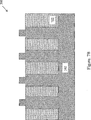
Jeder in
Die Breite der oberen Rechtecke ist als W1 bezeichnet und die Breite des unteren Rechtecks ist als W2 bezeichnet. Die tatsächlichen Dimensionen von W1 und W2 werden durch die Design-Regeln und die Skala des verwendeten Halbleiterprozesses bestimmt. Gemäß einer Ausführungsform kann das Verhältnis von W2 zu W1 größer als oder gleich 1,5 sein. Ein vorteilhaftes Merkmal dessen, ein breiteres unteres Rechteck zu haben, ist, dass der Quellwiderstand des FinFET verbessert wird, da die größere Breite des unteren Rechtecks dazu beiträgt, den Quellwiderstand zu verringern.The width of the upper rectangles is designated W1 and the width of the lower rectangle is designated W2. The actual dimensions of W1 and W2 are determined by the design rules and the scale of the semiconductor process used. In one embodiment, the ratio of W2 to W1 may be greater than or equal to 1.5. An advantageous feature of having a wider lower rectangle is that the source resistance of the FinFET is improved because the larger width of the lower rectangle helps to reduce the source resistance.
Um eine Transistor-Schwelleneinstellung, ein Anti-Durchgreifen (anti-punch through) und eine Wannenisolation zu verbessern, können der obere Bereich des oberen Rechtecks (z. B. Rechteck
Wie in
Die STI-Strukturen (z. B. das Isolationsgebiet
Ein vorteilhaftes Merkmal dessen, eine umgekehrt T-förmige Finne zu haben, ist, dass eine umgekehrt T-förmige Finne eine größere Angriffsfläche für ihre entsprechenden Kontaktstopfen bereitstellt. Im Ergebnis kann der Kontaktwiderstand verringert werden. Ein derart verringerter Kontaktwiderstand trägt dazu bei, die Geschwindigkeit und die Funktion des FinFET mit einer umgekehrt T-förmigen Finne zu verbessern.An advantageous feature of having an inverted T-shaped fin is that an inverted T-shaped fin provides a larger engagement surface for their respective contact plugs. As a result, the contact resistance can be reduced. Such a reduced contact resistance helps to improve the speed and function of the FinFET with an inverted T-shaped fin.
Es sollte angemerkt werden, dass die in
Nachdem die Maskenschicht
Während
Der Bildungsprozess des in
Das gestrichelte Rechteck
Wie in
Zusätzlich kann ein anderes Material, welches eine andere Gitterkonstante als das Kanalgebiet aufweist, eingesetzt werden, um das Drain-/Source-Gebiet (z. B. Drain-/Source-Gebiet
Ein vorteilhaftes Merkmal dessen, eine Gitterfehlanpassung zwischen dem Drain-/Source-Gebiet und denn Kanalgebiet zu haben, ist, dass die Gitterfehlanpassung zwischen dem Source-/Drain-Gebiet und dem Kanalgebiet dem Kanalgebiet eine Verspannung verleiht, wodurch die Trägerbeweglichkeit und die Gesamtleistung der Vorrichtung verbessert wird.An advantageous feature of having a lattice mismatch between the drain / source region and the channel region is that the lattice mismatch between the source / drain region and the channel region confers the channel region, thereby increasing carrier mobility and overall performance Device is improved.
Nachdem die Drain-/Source-Gebiete gebildet wurden, kann gemäß einer Ausführungsform ein optionaler Silizid-Prozess verwendet werden, um Silizidkontakte (nicht gezeigt) entlang der Drain-/Source-Gebiete zu bilden. Die Silizidkontakte können Nickel, Kobalt, Platin oder Erbium umfassen, um die Höhe der Schottky-Barriere des Kontaktes zu verringern. Allerdings können auch andere üblicherweise verwendete Materialien, wie beispielsweise Titan, Palladium usw. verwendet werden. Der Silizid-Prozess kann unter Verwendung geeigneter Techniken implementiert sein. Zum Beispiel kann die Silizidierung durchgeführt werden durch eine Blanket-Abscheidung einer geeigneten Metallschicht, gefolgt von einem Temper-Schritt, wodurch bewirkt wird, dass das Metall mit dem darunter liegenden freigelegten Silizium reagiert. Nicht reagiertes Metall wird dann durch eine geeignete Technik, wie beispielsweise einen selektiven Ätzprozess entfernt und ein zweites Tempern kann dann zur Silizidphaseneinstellung durchgeführt werden. Die Dicke der Silizidkontakte kann zwischen etwa 5 nm und etwa 50 nm sein.After the drain / source regions have been formed, according to one embodiment, an optional silicide process may be used to form silicide contacts (not shown) along the drain / source regions. The silicide contacts may include nickel, cobalt, platinum or erbium to reduce the height of the Schottky barrier of the contact. However, other commonly used materials such as titanium, palladium, etc. may also be used. The silicide process may be implemented using appropriate techniques. For example, the silicidation may be performed by blanket deposition of a suitable metal layer, followed by an annealing step, causing the metal to react with the underlying exposed silicon. Unreacted metal is then removed by a suitable technique, such as a selective etch process, and a second anneal can then be performed for silicide phase adjustment. The thickness of the silicide contacts may be between about 5 nm and about 50 nm.
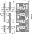
Die obere Stufe umfasst zwei Finnenlinien (z. B. Finnenlinien
Es sollte angemerkt werden, dass die Kombination von zwei verschiedenen Finnenstrukturen in einer Halbleitervorrichtung, wie in
Wie in
In einer (nicht gezeigten) SRAM-Anordnung, welche die 6T-SRAM-Zellen verwendet, sind die Zellen in Reihen und Spalten angeordnet. Die Spalten der SRAM-Anordnung sind durch Bit-Leitungspaare, nämlich eine erste Bit-Leitung BL und eine zweite Bit-Leitung BLB gebildet. Zusätzlich sind die Zellen der SRAM-Anordnung zwischen den entsprechenden Bit-Leitungspaaren angeordnet. Wie in
Wie in
Wie in denn Schaltungsdiagramm in
Wenn die Pass-Gate-Transistoren PG1 und PG2 inaktiv sind, wird die SRAM-Zelle
Während einer Schreiboperation werden die Bit-Leitungen BL und BLB auf entgegengesetzte logische Werte gemäß den neuen Daten, welche in die SRAM-Zelle
Nachdem die SRAM-Zelle
Während einer Schreiboperation werden sowohl BL als auch BLB der SRAM-Zelle
Während einer Leseoperation wird eine mit dem Speicherknoten, welcher eine logische „0” speichert, gekoppelte Bit-Leitung durch einen eingeschalteten Pass-Gate-Transistor PG1 und PG2 auf eine niedrigere Spannung entladen. Währenddessen bleibt die andere Bit-Leitung bei der vorgeladenen Spannung, da kein Entladepfad zwischen der anderen Bit-Leitung und dem Speicherknoten, welcher eine logische „1” speichert, vorhanden ist. Die Differenzspannung zwischen BL und BLB (ungefähr in einem Bereich von 50 bis 100 mV) wird durch einen (nicht gezeigten) Sense-Verstärker erfasst. Darüber hinaus verstärkt der Sense-Verstärker die Differenzspannung und berichtet den logischen Zustand der Speicherzelle über einen Datenpuffer.During a read operation, a bit line coupled to the storage node storing a logic "0" is discharged to a lower voltage by a turned-on pass gate transistor PG1 and PG2. Meanwhile, the other bit line remains at the precharged voltage because there is no discharge path between the other bit line and the storage node storing a logical "1". The difference voltage between BL and BLB (approximately in a range of 50 to 100 mV) is detected by a sense amplifier (not shown). In addition, the sense amplifier amplifies the differential voltage and reports the logic state of the memory cell via a data buffer.
Zwei vertikale gestrichelte Linien, welche die SRAM-Zelle schneiden, zeigen Grenzen zwischen einer p-Typ-Wanne in dem Substrat und einer n-Typ-Wanne in dem Substrat an, in welchen jeweilige Finnenlinien gebildet sind. Ein Fachmann erkennt leicht, dass ein Drain-/Source-Gebiet eines Transistors im Allgemeinen mit einem zu dem Dotiertyp der Wanne, in welchem das Drain-/Source-Gebiet gebildet ist, entgegengesetzten Dotiertyp dotiert ist. Zum Beispiel ist ein Source-/Drain-Gebiet im Allgemeinen p-Typ-dotiert, wenn die Wanne, in welcher der aktive Bereich gebildet ist, eine n-Typ-Wanne ist.Two vertical dashed lines intersecting the SRAM cell indicate boundaries between a p-type well in the substrate and an n-type well in the substrate in which respective fin lines are formed. One skilled in the art will readily recognize that a drain / source region of a transistor is generally doped with a dopant type opposite to the doping type of the well in which the drain / source region is formed. For example, a source / drain region is generally p-type doped when the well in which the active region is formed is an n-type well.
Wie in
Wie in
Verschiedene Kontakte werden eingesetzt, um Komponenten in der SRAM-Zelle zu koppeln. Ein Wortleitungskontakt WL (nicht gezeigt) kann an das Gate des Pass-Gate-Transistors PG1 gekoppelt sein und ein anderer Wortleitungskontakt WL (nicht gezeigt) ist mit dem Gate des Pass-Gate-Transistors PG2 gekoppelt. Ein Bit-Leitungskontakt BL ist mit dem Drain des Pass-Gate-Transistors PG1 gekoppelt und ein komplementärer Bit-Leitungskontakt BLB ist mit dem Drain des Pass-Gate-Transistors PG2 gekoppelt.Various contacts are used to couple components in the SRAM cell. A word line contact WL (not shown) may be coupled to the gate of the pass gate transistor PG1, and another word line contact WL (not shown) is coupled to the gate of the pass gate transistor PG2. A bit line contact BL is coupled to the drain of the pass gate transistor PG1, and a complementary bit line contact BLB is coupled to the drain of the pass gate transistor PG2.
Ein Leistungsquellenkontakt VCC ist mit dem Source des Pull-up-Transistors PU1 gekoppelt und ein anderer Leistungsquellenkontakt VCC ist mit dem Source des Pull-up-Transistors PU2 gekoppelt. Ein Massekontakt VSS ist mit dem Source des Pull-down-Transistors PD1 gekoppelt und ein anderer Massekontakt VSS ist mit dem Source des Pull-down-Transistors PD2 gekoppelt. Ein Speicherknotenkontakt SN koppelt das Source des Transistors PG1 und die Drains der Transistoren PD1 und PU1 zusammen. Ein anderer Speicherknotenkontakt SNB koppelt das Source des Transistors PG2 und die Drains der Transistoren PD2 und PU2 zusammen.A power source contact VCC is coupled to the source of the pull-up transistor PU1, and another power source contact VCC is coupled to the source of the pull-up transistor PU2. A ground contact VSS is coupled to the source of the pull-down transistor PD1 and another ground contact VSS is coupled to the source of the pull-down transistor PD2. A storage node contact SN couples the source of the transistor PG1 and the drains of the transistors PD1 and PU1 together. Another storage node contact SNB couples the source of transistor PG2 and the drains of transistors PD2 and PU2 together.
Die Finnen
Die Querschnittsansicht
Das gestrichelte Rechteck
Obwohl Ausführungsformen der vorliegenden Offenbarung und deren Vorteile im Detail beschrieben wurden, sollte verstanden werden, dass verschiedene Änderungen, Ersetzungen und Veränderungen hierin durchgeführt werden können, ohne von dem Umfang der Offenbarung, wie er durch die beigefügten Ansprüche definiert ist, abzuweichen.Although embodiments of the present disclosure and their advantages have been described in detail, it should be understood that various changes, substitutions and alterations can be made herein without departing from the scope of the disclosure as defined by the appended claims.
Darüber hinaus ist nicht beabsichtigt, dass der Umfang der vorliegenden Anmeldung durch die einzelnen Ausführungsformen des Prozesses, der Maschine, des Herstellens, der Zusammensetzung von Materie, Mitteln, Verfahren und Schritten, die in der Beschreibung beschrieben sind, beschränkt ist. Wie ein Fachmann ausgehend von der vorliegenden Offenbarung leicht anerkennen wird, können Prozesse, Maschinen, ein Herstellen, Zusammensetzungen von Materie, Mitteln, Verfahren oder Schritten, welche gegenwärtig existieren oder zu einem späteren Zeitpunkt entwickelt werden, und welche im Wesentlichen die gleiche Funktion erfüllen oder im Wesentlichen das gleiche Ergebnis wie die entsprechenden hierin beschriebenen Ausführungsformen erreichen, gemäß der vorliegenden Offenbarung verwendet werden. Demgemäß ist beabsichtigt, dass die beigefügten Ansprüche innerhalb ihres Umfangs derartige Prozesse, Maschinen, Herstellen, Zusammensetzungen von Materie, Mitteln, Verfahren und Schritten, umfassen.Furthermore, it is not intended that the scope of the present application be limited by the particular embodiments of the process, the machine, the making, the composition of matter, means, methods and steps described in the specification. As one of ordinary skill in the art will readily appreciate from the present disclosure, processes, machines, manufacturing, compositions of matter, means, methods, or steps that currently exist or may be developed at a later time, and which perform substantially the same function, or achieve substantially the same result as the corresponding embodiments described herein, may be used in accordance with the present disclosure. Accordingly, it is intended that the appended claims encompass within their scope such processes, machines, making, compositions of matter, means, methods, and steps.
Claims (20)
Applications Claiming Priority (2)
| Application Number | Priority Date | Filing Date | Title |
|---|---|---|---|
| US13/446,199 US9368388B2 (en) | 2012-04-13 | 2012-04-13 | Apparatus for FinFETs |
| US13/446,199 | 2012-04-13 |
Publications (2)
| Publication Number | Publication Date |
|---|---|
| DE102013103057A1 true DE102013103057A1 (en) | 2013-10-17 |
| DE102013103057B4 DE102013103057B4 (en) | 2023-04-06 |
Family
ID=49232312
Family Applications (1)
| Application Number | Title | Priority Date | Filing Date |
|---|---|---|---|
| DE102013103057.2A Active DE102013103057B4 (en) | 2012-04-13 | 2013-03-26 | Semiconductor device using FinFETs with two-level fins |
Country Status (4)
| Country | Link |
|---|---|
| US (2) | US9368388B2 (en) |
| KR (1) | KR101381096B1 (en) |
| CN (1) | CN103378135B (en) |
| DE (1) | DE102013103057B4 (en) |
Cited By (6)
| Publication number | Priority date | Publication date | Assignee | Title |
|---|---|---|---|---|
| DE102013108385B3 (en) * | 2013-07-17 | 2015-01-22 | Taiwan Semiconductor Manufacturing Company, Ltd. | Manufacturing method and semiconductor device with thermal adjustment of tension |
| US9006842B2 (en) | 2013-05-30 | 2015-04-14 | Taiwan Semiconductor Manufacturing Company, Ltd. | Tuning strain in semiconductor devices |
| US9224849B2 (en) | 2012-12-28 | 2015-12-29 | Taiwan Semiconductor Manufacturing Company, Ltd. | Transistors with wrapped-around gates and methods for forming the same |
| DE102014119642A1 (en) * | 2014-10-29 | 2016-05-04 | Taiwan Semiconductor Manufacturing Company, Ltd. | FINFETS WITH A SOURCE / DRAIN COVER |
| DE102016101112B4 (en) | 2015-09-04 | 2018-03-22 | Taiwan Semiconductor Manufacturing Co., Ltd. | FINFET COMPONENT AND METHOD FOR THE PRODUCTION THEREOF |
| US10164071B2 (en) | 2015-09-04 | 2018-12-25 | Taiwan Semiconductor Manufacturing Co., Ltd. | FinFET device and fabricating method thereof |
Families Citing this family (46)
| Publication number | Priority date | Publication date | Assignee | Title |
|---|---|---|---|---|
| US20140106529A1 (en) * | 2012-10-16 | 2014-04-17 | Stmicroelectronics (Crolles 2) Sas | Finfet device with silicided source-drain regions and method of making same using a two step anneal |
| US8697536B1 (en) | 2012-11-27 | 2014-04-15 | International Business Machines Corporation | Locally isolated protected bulk finfet semiconductor device |
| US8946063B2 (en) * | 2012-11-30 | 2015-02-03 | International Business Machines Corporation | Semiconductor device having SSOI substrate with relaxed tensile stress |
| GB2529953B (en) * | 2013-06-28 | 2020-04-01 | Intel Corp | Nanostructures and nanofeatures with Si (111) planes on Si (100) wafers for III-N epitaxy |
| US9293587B2 (en) | 2013-07-23 | 2016-03-22 | Globalfoundries Inc. | Forming embedded source and drain regions to prevent bottom leakage in a dielectrically isolated fin field effect transistor (FinFET) device |
| US9196613B2 (en) * | 2013-11-19 | 2015-11-24 | International Business Machines Corporation | Stress inducing contact metal in FinFET CMOS |
| KR102193493B1 (en) * | 2014-02-03 | 2020-12-21 | 삼성전자주식회사 | Semiconductor devices and methods of manufacturing the same |
| KR102158962B1 (en) * | 2014-05-08 | 2020-09-24 | 삼성전자 주식회사 | Semiconductor device and method for fabricating the same |
| KR102227128B1 (en) * | 2014-09-03 | 2021-03-12 | 삼성전자주식회사 | Semiconductor device and method for fabricating the same |
| KR102235614B1 (en) * | 2014-09-17 | 2021-04-02 | 삼성전자주식회사 | Integrated circuit device and method of manufacturing the same |
| KR102255174B1 (en) | 2014-10-10 | 2021-05-24 | 삼성전자주식회사 | Semiconductor device having active region and method of forming the same |
| KR102274750B1 (en) | 2015-01-27 | 2021-07-07 | 삼성전자주식회사 | Method for fabricating semiconductor device |
| US9502673B2 (en) * | 2015-03-31 | 2016-11-22 | International Business Machines Corporation | Transistor devices with tapered suspended vertical arrays of carbon nanotubes |
| KR102372167B1 (en) * | 2015-04-24 | 2022-03-07 | 삼성전자주식회사 | Semiconductor device |
| US9799730B2 (en) | 2015-05-28 | 2017-10-24 | International Business Machines Corporation | FINFETs with high quality source/drain structures |
| KR102449901B1 (en) | 2015-06-23 | 2022-09-30 | 삼성전자주식회사 | Integrated circuit device and method for manufacturing the same |
| US20170084616A1 (en) | 2015-09-18 | 2017-03-23 | Samsung Electronics Co., Ltd. | Semiconductor Devices Including FINFET Structures with Increased Gate Surface |
| US9922975B2 (en) | 2015-10-05 | 2018-03-20 | Taiwan Semiconductor Manufacturing Co., Ltd. | Integrated circuit having field-effect trasistors with dielectric fin sidewall structures and manufacturing method thereof |
| KR102427326B1 (en) | 2015-10-26 | 2022-08-01 | 삼성전자주식회사 | Semiconductor device and method for manufacturing the same |
| KR102366953B1 (en) | 2016-01-06 | 2022-02-23 | 삼성전자주식회사 | Semiconductor device and method of fabricating the same |
| US10290634B2 (en) * | 2016-01-20 | 2019-05-14 | Globalfoundries Inc. | Multiple threshold voltages using fin pitch and profile |
| JP6620034B2 (en) * | 2016-02-24 | 2019-12-11 | ルネサスエレクトロニクス株式会社 | Manufacturing method of semiconductor device |
| US9865504B2 (en) | 2016-03-04 | 2018-01-09 | Taiwan Semiconductor Manufacturing Company, Ltd. | Semiconductor device and manufacturing method thereof |
| US9799660B1 (en) * | 2016-05-11 | 2017-10-24 | Globalfoundries Inc. | Stable and reliable FinFET SRAM with improved beta ratio |
| US9640667B1 (en) * | 2016-05-17 | 2017-05-02 | International Business Machines Corporation | III-V vertical field effect transistors with tunable bandgap source/drain regions |
| CN107492549A (en) * | 2016-06-12 | 2017-12-19 | 中芯国际集成电路制造(上海)有限公司 | Transistor and forming method |
| US10269784B2 (en) | 2016-07-01 | 2019-04-23 | Taiwan Semiconductor Manufacturing Co., Ltd. | Integrated circuit layout and method of configuring the same |
| US9824921B1 (en) * | 2016-07-06 | 2017-11-21 | Globalfoundries Inc. | Method and apparatus for placing a gate contact inside a semiconductor active region having high-k dielectric gate caps |
| US9941278B2 (en) * | 2016-07-06 | 2018-04-10 | Globalfoundries Inc. | Method and apparatus for placing a gate contact inside an active region of a semiconductor |
| KR102483546B1 (en) | 2016-11-28 | 2023-01-02 | 삼성전자주식회사 | Semiconductor devices having a vertical channel |
| US10084066B2 (en) * | 2016-11-29 | 2018-09-25 | Taiwan Semiconductor Manufacturing Co., Ltd. | Semiconductor device and manufacturing method thereof |
| DE102017126881B4 (en) | 2016-12-15 | 2024-04-25 | Taiwan Semiconductor Manufacturing Co., Ltd. | FinFET structures and methods for their formation |
| US11476349B2 (en) * | 2016-12-15 | 2022-10-18 | Taiwan Semiconductor Manufacturing Company, Ltd. | FinFET structures and methods of forming the same |
| US10763280B2 (en) * | 2017-05-31 | 2020-09-01 | Taiwan Semiconductor Manufacturing Co., Ltd. | Hybrid FinFET structure |
| CN108987395B (en) * | 2017-05-31 | 2022-12-16 | 台湾积体电路制造股份有限公司 | Semiconductor device with a plurality of semiconductor chips |
| US10290639B2 (en) * | 2017-09-12 | 2019-05-14 | Globalfoundries Inc. | VNW SRAM with trinity cross-couple PD/PU contact and method for producing the same |
| US10510894B2 (en) * | 2017-11-30 | 2019-12-17 | Taiwan Semiconductor Manufacturing Co., Ltd. | Isolation structure having different distances to adjacent FinFET devices |
| US10319581B1 (en) * | 2017-11-30 | 2019-06-11 | Taiwan Semiconductor Manufacturing Co., Ltd. | Cut metal gate process for reducing transistor spacing |
| US10269932B1 (en) * | 2018-01-18 | 2019-04-23 | Globalfoundries Inc. | Asymmetric formation of epi semiconductor material in source/drain regions of FinFET devices |
| US10790184B2 (en) | 2018-09-28 | 2020-09-29 | Taiwan Semiconductor Manufacturing Co., Ltd. | Isolation with multi-step structure for FinFET device and method of forming the same |
| US11264268B2 (en) | 2018-11-29 | 2022-03-01 | Taiwan Semiconductor Mtaiwananufacturing Co., Ltd. | FinFET circuit devices with well isolation |
| US10964784B2 (en) * | 2019-04-18 | 2021-03-30 | Taiwan Semiconductor Manufacturing Co., Ltd. | Integrated circuit device and manufacturing method thereof |
| US11387365B2 (en) | 2020-04-01 | 2022-07-12 | Taiwan Semiconductor Manufacturing Co., Ltd. | Method of manufacturing a semiconductor device for recessed fin structure having rounded corners |
| KR102822858B1 (en) * | 2020-06-16 | 2025-06-20 | 삼성전자주식회사 | Semiconductor device |
| US12356608B2 (en) | 2021-09-17 | 2025-07-08 | Changxin Memory Technologies, Inc. | Semiconductor structure and manufacturing method thereof |
| CN116133398B (en) * | 2021-09-17 | 2025-07-25 | 长鑫存储技术有限公司 | Semiconductor structure and manufacturing method thereof |
Family Cites Families (26)
| Publication number | Priority date | Publication date | Assignee | Title |
|---|---|---|---|---|
| JP2005064500A (en) * | 2003-08-14 | 2005-03-10 | Samsung Electronics Co Ltd | Multi-structure silicon fin and manufacturing method |
| KR100496891B1 (en) * | 2003-08-14 | 2005-06-23 | 삼성전자주식회사 | Silicon fin for finfet and method for fabricating the same |
| KR100555518B1 (en) * | 2003-09-16 | 2006-03-03 | 삼성전자주식회사 | Double gate field effect transistor and its manufacturing method |
| US7385247B2 (en) * | 2004-01-17 | 2008-06-10 | Samsung Electronics Co., Ltd. | At least penta-sided-channel type of FinFET transistor |
| US7154118B2 (en) * | 2004-03-31 | 2006-12-26 | Intel Corporation | Bulk non-planar transistor having strained enhanced mobility and methods of fabrication |
| JPWO2006006438A1 (en) * | 2004-07-12 | 2008-04-24 | 日本電気株式会社 | Semiconductor device and manufacturing method thereof |
| KR100725951B1 (en) | 2005-08-23 | 2007-06-11 | 경북대학교 산학협력단 | CMOS element with well structure |
| KR100675290B1 (en) | 2005-11-24 | 2007-01-29 | 삼성전자주식회사 | Method for manufacturing semiconductor device having multi-channel field effect transistor and pin field effect transistor and related device |
| DE102006001680B3 (en) * | 2006-01-12 | 2007-08-09 | Infineon Technologies Ag | Manufacturing method for a FinFET transistor arrangement and corresponding FinFET transistor arrangement |
| US7745319B2 (en) * | 2006-08-22 | 2010-06-29 | Micron Technology, Inc. | System and method for fabricating a fin field effect transistor |
| US7880232B2 (en) * | 2006-11-01 | 2011-02-01 | Micron Technology, Inc. | Processes and apparatus having a semiconductor fin |
| JP2008300384A (en) * | 2007-05-29 | 2008-12-11 | Elpida Memory Inc | Semiconductor device and manufacturing method thereof |
| US8174073B2 (en) * | 2007-05-30 | 2012-05-08 | Taiwan Semiconductor Manufacturing Co., Ltd. | Integrated circuit structures with multiple FinFETs |
| TWI343633B (en) | 2007-08-29 | 2011-06-11 | Nanya Technology Corp | Method of forming a self-aligned finfet structure |
| US8058692B2 (en) | 2008-12-29 | 2011-11-15 | Taiwan Semiconductor Manufacturing Company, Ltd. | Multiple-gate transistors with reverse T-shaped fins |
| US8264021B2 (en) | 2009-10-01 | 2012-09-11 | Taiwan Semiconductor Manufacturing Company, Ltd. | Finfets and methods for forming the same |
| US8472227B2 (en) * | 2010-01-27 | 2013-06-25 | Taiwan Semiconductor Manufacturing Company, Ltd. | Integrated circuits and methods for forming the same |
| US8294212B2 (en) * | 2009-09-18 | 2012-10-23 | Taiwan Semiconductor Manufacturing Company, Ltd. | Methods and apparatus for SRAM bit cell with low standby current, low supply voltage and high speed |
| US8426923B2 (en) | 2009-12-02 | 2013-04-23 | Taiwan Semiconductor Manufacturing Company, Ltd. | Multiple-gate semiconductor device and method |
| US8263451B2 (en) | 2010-02-26 | 2012-09-11 | Taiwan Semiconductor Manufacturing Company, Ltd. | Epitaxy profile engineering for FinFETs |
| US8399931B2 (en) * | 2010-06-30 | 2013-03-19 | Taiwan Semiconductor Manufacturing Company, Ltd. | Layout for multiple-fin SRAM cell |
| US8582352B2 (en) * | 2011-12-06 | 2013-11-12 | Taiwan Semiconductor Manufacturing Company, Ltd. | Methods and apparatus for FinFET SRAM cells |
| US8987831B2 (en) * | 2012-01-12 | 2015-03-24 | Taiwan Semiconductor Manufacturing Company, Ltd. | SRAM cells and arrays |
| US20130200483A1 (en) * | 2012-02-08 | 2013-08-08 | United Microelectronics Corp. | Fin structure and method of forming the same |
| US8729634B2 (en) * | 2012-06-15 | 2014-05-20 | Taiwan Semiconductor Manufacturing Company, Ltd. | FinFET with high mobility and strain channel |
| US20150014808A1 (en) * | 2013-07-11 | 2015-01-15 | United Microelectronics Corp. | Semiconductor structure and fabrication method thereof |
-
2012
- 2012-04-13 US US13/446,199 patent/US9368388B2/en active Active
- 2012-06-11 KR KR1020120062144A patent/KR101381096B1/en active Active
- 2012-06-27 CN CN201210217511.XA patent/CN103378135B/en active Active
-
2013
- 2013-03-26 DE DE102013103057.2A patent/DE102013103057B4/en active Active
-
2016
- 2016-06-09 US US15/178,045 patent/US10068905B2/en active Active
Cited By (17)
| Publication number | Priority date | Publication date | Assignee | Title |
|---|---|---|---|---|
| US9224849B2 (en) | 2012-12-28 | 2015-12-29 | Taiwan Semiconductor Manufacturing Company, Ltd. | Transistors with wrapped-around gates and methods for forming the same |
| US9006842B2 (en) | 2013-05-30 | 2015-04-14 | Taiwan Semiconductor Manufacturing Company, Ltd. | Tuning strain in semiconductor devices |
| US9419098B2 (en) | 2013-05-30 | 2016-08-16 | Taiwan Semiconductor Manufacturing Company, Ltd. | Tuning strain in semiconductor devices |
| US9941404B2 (en) | 2013-05-30 | 2018-04-10 | Taiwan Semiconductor Manufacturing Company, Ltd. | Tuning strain in semiconductor devices |
| DE102013108385B3 (en) * | 2013-07-17 | 2015-01-22 | Taiwan Semiconductor Manufacturing Company, Ltd. | Manufacturing method and semiconductor device with thermal adjustment of tension |
| US9349850B2 (en) | 2013-07-17 | 2016-05-24 | Taiwan Semiconductor Manufacturing Company, Ltd. | Thermally tuning strain in semiconductor devices |
| US9871141B2 (en) | 2013-07-17 | 2018-01-16 | Taiwan Semiconductor Manufacturing Company, Ltd. | Thermally tuning strain in semiconductor devices |
| US9941406B2 (en) | 2014-08-05 | 2018-04-10 | Taiwan Semiconductor Manufacturing Company, Ltd. | FinFETs with source/drain cladding |
| DE102014119642A1 (en) * | 2014-10-29 | 2016-05-04 | Taiwan Semiconductor Manufacturing Company, Ltd. | FINFETS WITH A SOURCE / DRAIN COVER |
| DE102014119642B4 (en) * | 2014-10-29 | 2018-01-11 | Taiwan Semiconductor Manufacturing Company, Ltd. | FINFETS WITH A SOURCE / DRAIN COVER |
| US10269964B2 (en) | 2014-10-29 | 2019-04-23 | Taiwan Semiconductor Manufacturing Company | FinFETs with source/drain cladding |
| US10868186B2 (en) | 2014-10-29 | 2020-12-15 | Taiwan Semiconductor Manufacturing Company, Ltd. | FinFETs with source/drain cladding |
| US10707349B2 (en) | 2014-10-29 | 2020-07-07 | Taiwan Semiconductor Manufacturing Company, Ltd. | FinFETs with source/drain cladding |
| DE102016101112B4 (en) | 2015-09-04 | 2018-03-22 | Taiwan Semiconductor Manufacturing Co., Ltd. | FINFET COMPONENT AND METHOD FOR THE PRODUCTION THEREOF |
| US10326006B2 (en) | 2015-09-04 | 2019-06-18 | Taiwan Semiconductor Manufacturing Co., Ltd. | FinFET device and fabricating method thereof |
| US10164059B2 (en) | 2015-09-04 | 2018-12-25 | Taiwan Semiconductor Manufacturing Co., Ltd. | FinFET device and fabricating method thereof |
| US10164071B2 (en) | 2015-09-04 | 2018-12-25 | Taiwan Semiconductor Manufacturing Co., Ltd. | FinFET device and fabricating method thereof |
Also Published As
| Publication number | Publication date |
|---|---|
| KR101381096B1 (en) | 2014-04-02 |
| US10068905B2 (en) | 2018-09-04 |
| CN103378135A (en) | 2013-10-30 |
| CN103378135B (en) | 2017-04-12 |
| US9368388B2 (en) | 2016-06-14 |
| DE102013103057B4 (en) | 2023-04-06 |
| US20130270652A1 (en) | 2013-10-17 |
| KR20130116140A (en) | 2013-10-23 |
| US20160293604A1 (en) | 2016-10-06 |
Similar Documents
| Publication | Publication Date | Title |
|---|---|---|
| DE102013103057B4 (en) | Semiconductor device using FinFETs with two-level fins | |
| DE102012108290B4 (en) | Structure for FinFETs as well as system of SRAM cells and memory cell having such a structure | |
| DE102013105074B4 (en) | Integrated circuit that includes FinFETs with different fin profiles | |
| DE102013104983B4 (en) | Cell layout for SRAM FinFET transistors | |
| DE102018100001B4 (en) | Fin-based stripe cell structure | |
| DE102008001534B4 (en) | Transistor with reduced charge carrier mobility and associated methods and SRAM cell with such transistors | |
| DE102008045037B4 (en) | Static RAM cell structure and multiple contact scheme for connecting dual-channel transistors | |
| DE102005001134B4 (en) | Junction-contact structures in semiconductor devices, particularly SRAM devices, and methods of making same | |
| DE602004010859T2 (en) | Method for fabricating a nanoscale resistance crosspoint memory device and device | |
| DE102013101816B4 (en) | Device for SRAM cells | |
| DE112006002913B4 (en) | Memory cell, method for its production and memory cell matrix | |
| DE10338986B4 (en) | SRAM device | |
| DE112004001864T5 (en) | Method and apparatus for improving the stability of a 6-transistor CMOS SRAM cell | |
| DE102004037087A1 (en) | Self-biasing transistor structure and SRAM cells with fewer than six transistors | |
| DE102008011797A1 (en) | Circuit has static random access memory storage element with storage cell and cross coupled inverter based on multi-gate-field effect transistors | |
| DE102010025395A1 (en) | Memory cell layout | |
| DE102009035409A1 (en) | Leakage current control in field effect transistors based on an implantation species introduced locally at the STI edge | |
| DE102019117897B4 (en) | SEMICONDUCTOR DEVICE FOR LOGIC AND MEMORY CO-OPTIMIZATION AND CIRCUIT | |
| DE112006001771T5 (en) | SRAM devices using tensile strained stress layers | |
| DE102008030853A1 (en) | Three-dimensional transistor with a dual-channel configuration | |
| DE102013202739A1 (en) | SRAM integrated circuits with buried saddle-shaped FINFET and method of making same | |
| DE102024100989B4 (en) | INTEGRATION OF STORAGE CELL AND LOGIC CELL | |
| DE19860119C2 (en) | SRAM semiconductor memory device | |
| DE112009001286B4 (en) | Method of fabricating random access memory cells based on gated lateral thyristors (GLTRAM) | |
| DE102023129095A1 (en) | MULTI-PORT SRAM STRUCTURES WITH CELL SIZE OPTIMIZATION |
Legal Events
| Date | Code | Title | Description |
|---|---|---|---|
| R012 | Request for examination validly filed | ||
| R016 | Response to examination communication | ||
| R016 | Response to examination communication | ||
| R018 | Grant decision by examination section/examining division | ||
| R020 | Patent grant now final | ||
| R079 | Amendment of ipc main class |
Free format text: PREVIOUS MAIN CLASS: H01L0029780000 Ipc: H10D0030600000 |