CN2631038Y - Integrated Circuit Package Assembly in Bare Die Form - Google Patents
Integrated Circuit Package Assembly in Bare Die Form Download PDFInfo
- Publication number
- CN2631038Y CN2631038Y CN03206602.3U CN03206602U CN2631038Y CN 2631038 Y CN2631038 Y CN 2631038Y CN 03206602 U CN03206602 U CN 03206602U CN 2631038 Y CN2631038 Y CN 2631038Y
- Authority
- CN
- China
- Prior art keywords
- integrated circuit
- circuit package
- crystalline form
- clubfoot
- chip
- Prior art date
- Legal status (The legal status is an assumption and is not a legal conclusion. Google has not performed a legal analysis and makes no representation as to the accuracy of the status listed.)
- Expired - Lifetime
Links
Images


Classifications
-
- H—ELECTRICITY
- H10—SEMICONDUCTOR DEVICES; ELECTRIC SOLID-STATE DEVICES NOT OTHERWISE PROVIDED FOR
- H10W—GENERIC PACKAGES, INTERCONNECTIONS, CONNECTORS OR OTHER CONSTRUCTIONAL DETAILS OF DEVICES COVERED BY CLASS H10
- H10W72/00—Interconnections or connectors in packages
- H10W72/50—Bond wires
- H10W72/551—Materials of bond wires
- H10W72/552—Materials of bond wires comprising metals or metalloids, e.g. silver
- H10W72/5522—Materials of bond wires comprising metals or metalloids, e.g. silver comprising gold [Au]
-
- H—ELECTRICITY
- H10—SEMICONDUCTOR DEVICES; ELECTRIC SOLID-STATE DEVICES NOT OTHERWISE PROVIDED FOR
- H10W—GENERIC PACKAGES, INTERCONNECTIONS, CONNECTORS OR OTHER CONSTRUCTIONAL DETAILS OF DEVICES COVERED BY CLASS H10
- H10W72/00—Interconnections or connectors in packages
- H10W72/50—Bond wires
- H10W72/551—Materials of bond wires
- H10W72/552—Materials of bond wires comprising metals or metalloids, e.g. silver
- H10W72/5524—Materials of bond wires comprising metals or metalloids, e.g. silver comprising aluminium [Al]
-
- H—ELECTRICITY
- H10—SEMICONDUCTOR DEVICES; ELECTRIC SOLID-STATE DEVICES NOT OTHERWISE PROVIDED FOR
- H10W—GENERIC PACKAGES, INTERCONNECTIONS, CONNECTORS OR OTHER CONSTRUCTIONAL DETAILS OF DEVICES COVERED BY CLASS H10
- H10W72/00—Interconnections or connectors in packages
- H10W72/851—Dispositions of multiple connectors or interconnections
- H10W72/853—On the same surface
- H10W72/865—Die-attach connectors and bond wires
-
- H—ELECTRICITY
- H10—SEMICONDUCTOR DEVICES; ELECTRIC SOLID-STATE DEVICES NOT OTHERWISE PROVIDED FOR
- H10W—GENERIC PACKAGES, INTERCONNECTIONS, CONNECTORS OR OTHER CONSTRUCTIONAL DETAILS OF DEVICES COVERED BY CLASS H10
- H10W90/00—Package configurations
- H10W90/701—Package configurations characterised by the relative positions of pads or connectors relative to package parts
- H10W90/721—Package configurations characterised by the relative positions of pads or connectors relative to package parts of bump connectors
- H10W90/726—Package configurations characterised by the relative positions of pads or connectors relative to package parts of bump connectors between a chip and a stacked lead frame, conducting package substrate or heat sink
-
- H—ELECTRICITY
- H10—SEMICONDUCTOR DEVICES; ELECTRIC SOLID-STATE DEVICES NOT OTHERWISE PROVIDED FOR
- H10W—GENERIC PACKAGES, INTERCONNECTIONS, CONNECTORS OR OTHER CONSTRUCTIONAL DETAILS OF DEVICES COVERED BY CLASS H10
- H10W90/00—Package configurations
- H10W90/701—Package configurations characterised by the relative positions of pads or connectors relative to package parts
- H10W90/731—Package configurations characterised by the relative positions of pads or connectors relative to package parts of die-attach connectors
- H10W90/736—Package configurations characterised by the relative positions of pads or connectors relative to package parts of die-attach connectors between a chip and a stacked lead frame, conducting package substrate or heat sink
-
- H—ELECTRICITY
- H10—SEMICONDUCTOR DEVICES; ELECTRIC SOLID-STATE DEVICES NOT OTHERWISE PROVIDED FOR
- H10W—GENERIC PACKAGES, INTERCONNECTIONS, CONNECTORS OR OTHER CONSTRUCTIONAL DETAILS OF DEVICES COVERED BY CLASS H10
- H10W90/00—Package configurations
- H10W90/701—Package configurations characterised by the relative positions of pads or connectors relative to package parts
- H10W90/751—Package configurations characterised by the relative positions of pads or connectors relative to package parts of bond wires
- H10W90/756—Package configurations characterised by the relative positions of pads or connectors relative to package parts of bond wires between a chip and a stacked lead frame, conducting package substrate or heat sink
Landscapes
- Structures Or Materials For Encapsulating Or Coating Semiconductor Devices Or Solid State Devices (AREA)
Abstract
Description
技术领域technical field
本实用新型属于积体电路封装组件,特别是一种裸晶形态的积体电路封装组件。The utility model belongs to an integrated circuit packaging assembly, in particular to an integrated circuit packaging assembly in the form of a bare crystal.
背景技术Background technique
传统的积体电路封装组件中,常见以引线框架(lead frame)作为封装组件中晶片电性导接介质,利用引线框架完成积体电路封装组件除了应符合单向表面结合的要求外,在不增加外部印刷电路板表面结合面积状态下或条件下,于特定场合需要能垂直向堆叠结合(stack mounting)。In traditional integrated circuit packaging components, it is common to use lead frames as the electrical connection medium for chips in package components. The use of lead frames to complete integrated circuit packaging components should meet the requirements of unidirectional surface bonding. In the state or condition of increasing the bonding area on the surface of the external printed circuit board, it is necessary to be able to vertically stack the bonding (stack mounting) in a specific occasion.
如图1所示,习知的以引线框架作为导接介质且能垂直向堆叠结合的积体电路封装组件1包括正面11形成电极端12的晶片10、具有数个形成内接端21接脚20的引线框架、数金属焊线40及封装胶体30。As shown in FIG. 1 , a conventional integrated circuit package assembly 1 that uses a lead frame as a conductive medium and can be vertically stacked and combined includes a
引线框架数接脚20的内接端21黏设于晶片10的正面11;数金属焊线40电性连接于晶片10的电极端12及引线框架接脚20的内接端21,且以压模(molding)形成封装胶体30以密封晶片10及引线框架接脚20的内接端21,并使接脚20内接端21具有显露于封装胶体30第一表面31以作为第一向表面接触点的显露表面23,接脚20的延伸端22系由封装胶体30第一表面31侧边延伸出并弯折成J形脚,延伸端22系形成于封装胶体30的第二表面32,以作为第二向表面接触点。因此,数个积体电路封装组件1系能垂直向堆叠。然而,引线框架数个接脚20的延伸端22系由封装胶体30悬空伸出,在成形后,任何碰撞均可能使接脚20的延伸端22歪斜,导致表面接合不良,所以接脚20的厚度要足够厚,以减轻歪斜程度,如此,连带使得积体电路封装组件1厚度较大,不宜高密度堆叠。The
另一种习知积体电路封装组件,如美国专利第5,894,108号专利揭示了晶片背面裸露,以降低整体封装组件的厚度的设计,其晶片系显露于封装胶体外,但其接脚的稳固性不如前述传统结构的接脚稳固,易于脱落,且仅能作单向表面接合,无法堆叠利用,运用领域有限。Another conventional integrated circuit packaging component, such as US Patent No. 5,894,108, discloses a design in which the back of the chip is exposed to reduce the thickness of the overall package component. The chip is exposed outside the packaging compound, but the stability of the pins The pins are not as stable as the aforementioned traditional structures, are easy to fall off, and can only be used for one-way surface bonding, which cannot be stacked and used, and the application field is limited.
发明内容Contents of the invention
本实用新型的目的是提供一种表面接合对位效果好、可垂直向高密度堆叠、厚度薄的裸晶形态的积体电路封装组件。The purpose of the utility model is to provide an integrated circuit packaging assembly in the shape of bare crystal with good surface bonding alignment effect, vertically high-density stacking, and thin thickness.
本实用新型包括晶片、金属引线框架及绝缘封装胶体;晶片具有形成数个电极端的正面及对应的背面;金属引线框架包含数个弯脚,每一弯脚形成延伸端;绝缘封装胶体结合晶片及弯脚;封装胶体具有第一表面及第二表面;晶片的背面系显露于封装胶体第一、二表面中之一的表面而呈裸晶形态;封装胶体第一、二表面中之一的表面周边形成数个容设并限定弯脚延伸端的限位缺口槽。The utility model includes a chip, a metal lead frame and an insulating encapsulation colloid; the chip has a front surface and a corresponding back surface forming several electrode terminals; the metal lead frame includes several bent legs, each of which forms an extension end; the insulating encapsulation colloid is combined with the chip and bent feet; the encapsulation compound has a first surface and a second surface; the back of the chip is exposed on one of the first and second surfaces of the encapsulation compound and is in the form of a bare crystal; the encapsulation compound is one of the first and second surfaces A plurality of position-limiting notch slots are formed around the surface to accommodate and limit the extension ends of the curved legs.
其中:in:
封装胶体由第一表面至第二表面的厚度系不大于0.6cm。The thickness of the encapsulant from the first surface to the second surface is not greater than 0.6 cm.
封装胶体由第一表面至第二表面的厚度系不大于0.4cm。The thickness of the encapsulant from the first surface to the second surface is not greater than 0.4cm.
限位缺口槽的深度不大于相对应弯脚延伸端的厚度。The depth of the limiting notch groove is not greater than the thickness of the extension end of the corresponding bent leg.
限位缺口槽呈具有斜向放大侧壁的开口扩张状。The limiting notch groove is in the shape of an opening with an obliquely enlarged side wall.
每一弯脚具有对应延伸端的内接端,内接端具有显露于封装胶体第一表面的显露表面。Each bent leg has an inner end corresponding to the extension end, and the inner end has an exposed surface exposed on the first surface of the encapsulant.
弯脚内接端具有借以与晶片电极端电性导通的端部;端部系形成于与内接端显露表面不相同的平面而完全被封装胶体包覆。The inner connection end of the bent pin has an end portion for electrical conduction with the electrode end of the chip; the end portion is formed on a plane different from the exposed surface of the inner connection end, and is completely covered by encapsulation glue.
弯脚内接端的端部贴附于内置贴片。The end of the inner terminal of the bent leg is attached to the built-in patch.
弯脚内接端的端部与晶片的电极端之间以数条金属焊线连接。The end of the inner terminal of the bent leg is connected with the electrode terminal of the chip by several metal welding wires.
晶片电极端设有导电凸块以电性连接晶片电极端及弯脚。The electrode end of the chip is provided with a conductive bump to electrically connect the electrode end of the chip and the bent pin.
由于本实用新型包括晶片、金属引线框架及绝缘封装胶体;晶片具有形成数个电极端的正面及对应的背面;金属引线框架包含数个弯脚,每一弯脚形成延伸端;绝缘封装胶体结合晶片及弯脚;封装胶体具有第一表面及第二表面;晶片的背面系显露于封装胶体第一、二表面中之一的表面而呈裸晶形态;封装胶体第一、二表面中之一的表面周边形成数个容设并限定弯脚延伸端的限位缺口槽。借由晶片背面显露及封装胶体的限位缺槽口,使弯脚延伸端容设并限定于封装胶体的限位缺槽口,能构成可垂直向堆叠且整体呈超薄形态,在相同高度下可高密度垂直向堆叠更多个裸晶形态的积体电路封装组件;不仅表面接合对位效果好,而且可垂直向高密度堆叠、厚度薄,从而达到本实用新型的目的。Because the utility model includes a chip, a metal lead frame and an insulating packaging colloid; the chip has a front surface and a corresponding back surface forming several electrode terminals; the metal lead frame includes several bent legs, each of which forms an extension; the insulating packaging colloid combines Chip and bent pin; the encapsulation compound has a first surface and a second surface; the back side of the chip is exposed on one of the first and second surfaces of the encapsulation compound and is in the form of a bare crystal; one of the first and second surfaces of the encapsulation compound A plurality of position-limiting notch grooves are formed around the surface of the surface to accommodate and limit the extension ends of the bent legs. With the exposure of the back of the chip and the limiting notch of the encapsulant, the extension end of the bent leg can be accommodated and limited to the limit notch of the encapsulant, which can be vertically stacked and the overall shape is ultra-thin, at the same height High-density vertical stacking of more bare-chip integrated circuit package components is possible; not only the surface bonding and alignment effect is good, but also vertical high-density stacking and thin thickness are possible, thereby achieving the purpose of the utility model.
附图说明Description of drawings
图1、为习知的积体电路封装组件结构示意剖视图。FIG. 1 is a schematic cross-sectional view of the structure of a conventional integrated circuit package assembly.
图2、为本实用新型实施例一结构示意剖视图。Fig. 2 is a schematic cross-sectional view of the structure of Embodiment 1 of the present utility model.
图3、为本实用新型实施例一结构示意俯视图。Fig. 3 is a schematic top view of the first embodiment of the utility model.
图4、为本实用新型实施例一结构示意仰视图。Fig. 4 is a schematic bottom view of the first embodiment of the utility model.
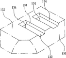
图5、为图2中A部局部放大图(显示缺口槽)。Fig. 5 is a partially enlarged view of part A in Fig. 2 (showing the notch groove).
图6、为数个本实用新型实施例一堆叠接合使用状态示意图。Fig. 6 is a schematic diagram of several embodiments of the present utility model-stacking and jointing use state.
图7、为本实用新型实施例一封装过程示意图。Fig. 7 is a schematic diagram of the encapsulation process of Embodiment 1 of the present utility model.
图8、为本实用新型实施例二结构示意剖视图。Fig. 8 is a schematic cross-sectional view of the second embodiment of the utility model.
具体实施方式Detailed ways
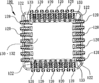
如图2、图3、图4所示,本实用新型裸晶形态的积体电路封装组件100包括晶片110、金属引线框架及绝缘封装胶体130。As shown in FIG. 2 , FIG. 3 , and FIG. 4 , the integrated
晶片110系选自微处理器、微控制器、各式记忆体、特殊应用积体电路或影像处理晶片,晶片110具有形成积体电路布局的正面111及对应的背面113。晶片110正面111系形成数个电极端(electrode)112,如平垫状焊垫(bondingpad)或凸起的凸块(bump),晶片110的电极端112系电性导接至引线框架。The
引线框架为铜、铁或合金等具有适当延展性的金属,其包含数个弯脚120,弯脚120呈U形,每一弯脚120区分为位于封装胶体130内、外的内接端121及延伸端122,内接端121具有显露于封装胶体130第一表面131的显露表面123,内接端121系以其端部124电性导通至晶片110的电极端112。如图2、图3所示,较佳系利用数条金线或铝线等金属焊线140连接于弯脚120内接端121的端部124与晶片110的电极端112之间,端部124系形成于与内接端121显露表面123不相同的平面,以使得端部124可完全被封装胶体130包覆而具有较佳稳固性,内接端121的显露表面123系显露于封装胶体130的第一表面131,可供第一向表面接合;如图2、图4所示,弯脚120的延伸端122系由封装胶体130的侧边延伸出并弯折至封装胶体130的第二表面132周边,以供第二向表面接合。The lead frame is a metal with proper ductility such as copper, iron or alloy, and it includes
封装胶体130系由热固性绝缘树脂以压模(molding)技术形成,封装胶体130系具有第一表面131及第二表面132。如图2、图3所示,晶片110的背面113系显露于封装胶体130的第一表面131而呈裸晶形态。弯脚120的内接端121显露表面123系形成于封装胶体130第一表面131周边,弯脚120的延伸端122系弯折至封装胶体130第二表面132周边。The
如图5、图7所示,封装胶体130第二表面132周边在压模时即形成数个限位缺口槽133,借由限位缺口槽133容设并限定弯脚120延伸端122,以达到弯脚120能准确对位表面接合的功效,更能达到垂直向高密度堆叠的运用,因此,可降低弯脚120所需要的结构强度,从而可将引线框架的厚度降低至约0.127cm,而习知的J形脚厚度要求为0.2cm,限位缺口槽133的深度以不大于相对应弯脚120延伸端120的厚度为较佳。如图5所示,限位缺口槽133呈具有斜向放大侧壁的开口扩张状,以有利于表面接合时,弯脚120延伸端122导引对位,也就是说,即使弯脚120的延伸端122有些许偏斜,在表面接合(surface mounting)时,弯脚120的延伸端122能被斜向侧壁正确导引修正至限位缺口槽133,在弯脚120密集排列设计下,弯脚120的延伸端122宽度应略窄于弯脚120内接端121的宽度。As shown in FIGS. 5 and 7 , several limiting
本实用新型裸晶形态的积体电路封装组件1借由晶片110背面113显露及呈U形弯脚120的设计,能构成可垂直向堆叠且整体呈超薄形态。The integrated circuit package assembly 1 in the form of bare crystal of the present invention can be vertically stacked and has an overall ultra-thin shape by virtue of the exposed
封装胶体130由第一表面131至第二表面132的厚度系不大于0.6cm,更可达到不大于0.4cm的程度。如此,如图6所示,在相同高度下可高密度垂直向堆叠更多个裸晶形态的积体电路封装组件100。此外,由于晶片110不被引线框架所承载,在封装后,晶片110如同“果冻”般固定于封装胶体130,使引线框架与晶片110无直接的结合关系,而是由封装胶体130结合晶片110及引线框架,可降低热应力对晶片110的影响。The thickness of the
如图7所示,本实用新型在制造过程中,晶片110背面113与引线框架系贴附于外置型胶带(external tape)150上,在电性连接晶片110与引线框架后,连同外置型胶带150一并置入压模模具,在形成封装胶体130时即成形限位缺口槽133,在撕离外置型胶带150后,便可将引线框架弯脚120的延伸端122弯折至封装胶体130的限位缺口槽133内,并使弯脚120的延伸端122以接触封装胶体130的第二表面132为较佳。As shown in Figure 7, in the manufacturing process of the present invention, the
实施例二Embodiment two
限位缺口槽133除了可形成于封装胶体130第二表面132外,亦可形成于封装胶体230的第一表面231以与晶片210的裸露的背面213位于同一表面上。In addition to being formed on the
如图8所示,本实用新型裸晶形态的积体电路封装组件200包括晶片210、金属引线框架及绝缘封装胶体230。As shown in FIG. 8 , the integrated
晶片210系选自微处理器、微控制器、各式记忆体、特殊应用积体电路或影像处理晶片,晶片210具有形成积体电路布局的正面211及对应的背面213。晶片210正面211系形成数个电极端(electrode)212。The
封装胶体230系由热固性绝缘树脂以压模(molding)技术形成,封装胶体230系具有第一表面231及第二表面232。The
引线框架为铜、铁或合金等具有适当延展性的金属,其包含数个弯脚220,弯脚220呈U形,每一弯脚220区分为位于封装胶体230内、外的内接端221及延伸端222。较佳地弯脚220内接端221系贴附有内置贴片(internal tape)242,弯脚220内接端221具有显露出封装胶体230第二表面232的显露表面223;弯脚220的延伸端222系由封装胶体230的侧边延伸出并弯折至封装胶体230的第一表面231周边的限位缺口槽233。The lead frame is a metal with proper ductility, such as copper, iron or alloy, which includes several
晶片210的背面213系显露于封装胶体230的第一表面231而呈裸晶形态;弯脚220的内接端221显露表面223系形成于封装胶体230第二表面232周边,弯脚220的延伸端222系弯折至封装胶体230第一表面231周边。弯脚220内接端221的端部224系形成于与内接端221显露表面223不相同的平面;晶片210电极端212利用覆晶(flip chip)或内引指接合(inner lead bonding)技术以导电凸块(bump)241与引线框架弯脚220内接端221的端部224电性连接。The
Claims (10)
Priority Applications (1)
| Application Number | Priority Date | Filing Date | Title |
|---|---|---|---|
| CN03206602.3U CN2631038Y (en) | 2003-07-29 | 2003-07-29 | Integrated Circuit Package Assembly in Bare Die Form |
Applications Claiming Priority (1)
| Application Number | Priority Date | Filing Date | Title |
|---|---|---|---|
| CN03206602.3U CN2631038Y (en) | 2003-07-29 | 2003-07-29 | Integrated Circuit Package Assembly in Bare Die Form |
Publications (1)
| Publication Number | Publication Date |
|---|---|
| CN2631038Y true CN2631038Y (en) | 2004-08-04 |
Family
ID=34288105
Family Applications (1)
| Application Number | Title | Priority Date | Filing Date |
|---|---|---|---|
| CN03206602.3U Expired - Lifetime CN2631038Y (en) | 2003-07-29 | 2003-07-29 | Integrated Circuit Package Assembly in Bare Die Form |
Country Status (1)
| Country | Link |
|---|---|
| CN (1) | CN2631038Y (en) |
Cited By (2)
| Publication number | Priority date | Publication date | Assignee | Title |
|---|---|---|---|---|
| CN101449375B (en) * | 2006-06-29 | 2012-01-18 | 英特尔公司 | Apparatus, system and method for wireless connection in integrated circuit package |
| CN101755336B (en) * | 2007-07-24 | 2013-08-28 | 美光科技公司 | Microelectronic die packages with metal leads, including metal leads for stacked die packages, and associated systems and methods |
-
2003
- 2003-07-29 CN CN03206602.3U patent/CN2631038Y/en not_active Expired - Lifetime
Cited By (2)
| Publication number | Priority date | Publication date | Assignee | Title |
|---|---|---|---|---|
| CN101449375B (en) * | 2006-06-29 | 2012-01-18 | 英特尔公司 | Apparatus, system and method for wireless connection in integrated circuit package |
| CN101755336B (en) * | 2007-07-24 | 2013-08-28 | 美光科技公司 | Microelectronic die packages with metal leads, including metal leads for stacked die packages, and associated systems and methods |
Similar Documents
| Publication | Publication Date | Title |
|---|---|---|
| US6841863B2 (en) | Ball grid array package with stacked center pad chips and method for manufacturing the same | |
| KR100226737B1 (en) | Semiconductor device stacked package | |
| US20100244278A1 (en) | Stacked multichip package | |
| TW200410386A (en) | Lead frame and method of producing the same, and resin-encapsulated semiconductor device and method of producing the same | |
| JP2001185651A (en) | Semiconductor device and method of manufacturing the same | |
| US6753599B2 (en) | Semiconductor package and mounting structure on substrate thereof and stack structure thereof | |
| JPH05283600A (en) | Semiconductor device and manufacture of the same | |
| JPH08186151A (en) | Semiconductor device and manufacturing method thereof | |
| CN101226586A (en) | Film packaging structure of fingerprint identifier | |
| JP2002217514A (en) | Multi-chip semiconductor device | |
| US20050224937A1 (en) | Exposed pad module integrated a passive device therein | |
| CN111009475B (en) | Packaging structure and packaging method of optical module | |
| CN2631038Y (en) | Integrated Circuit Package Assembly in Bare Die Form | |
| US20230275008A1 (en) | Semiconductor package with overlapping leads and die pad | |
| JPH1197570A (en) | Semiconductor device, method of manufacturing the same, and method of mounting semiconductor device | |
| CN1163960C (en) | ultra-thin package with high heat dissipation and manufacturing method thereof | |
| CN1197149C (en) | Encapsulation component with downturn spoiler structure | |
| JP2006066551A5 (en) | ||
| JP2000183275A (en) | Semiconductor device | |
| CN2376078Y (en) | Semiconductor Package Components | |
| KR100639700B1 (en) | Chip Scale Stacked Chip Packages | |
| CN101145549A (en) | Ball grid array packaging structure and packaging method thereof | |
| CN1362737A (en) | Semiconductor package with glue overflow prevention device | |
| CN2465328Y (en) | double sided chip package | |
| CN212182316U (en) | A carrier-free semiconductor stacked packaging structure |
Legal Events
| Date | Code | Title | Description |
|---|---|---|---|
| C14 | Grant of patent or utility model | ||
| GR01 | Patent grant | ||
| C17 | Cessation of patent right | ||
| CX01 | Expiry of patent term |
Expiration termination date: 20130729 Granted publication date: 20040804 |