具体实施方式Detailed ways
下面将结合本申请实施例中的附图,对本申请实施例中的技术方案进行清楚、完整地描述,显然,所描述的实施例仅仅是本申请一部分实施例,而不是全部的实施例。此外,在本申请中提及“实施例”或“实施方式”意味着,结合实施例或实施方式描述的特定特征、结构或特性可以包含在本申请的至少一个实施例中。在说明书中的各个位置出现该短语并不一定均是指相同的实施例,也不是与其它实施例互斥的独立的或备选的实施例。本领域技术人员显式地和隐式地理解的是,本申请所描述的实施例可以与其它实施例相结合。The technical solutions in the embodiments of the present application will be clearly and completely described below with reference to the drawings in the embodiments of the present application. Obviously, the described embodiments are only a part of the embodiments of the present application, but not all of the embodiments. Furthermore, reference in this application to an "embodiment" or an "implementation" means that a particular feature, structure, or characteristic described in connection with the example or implementation can be included in at least one embodiment of the application. The appearances of the phrase in various places in the specification are not necessarily all referring to the same embodiment, nor a separate or alternative embodiment that is mutually exclusive of other embodiments. It is explicitly and implicitly understood by those skilled in the art that the embodiments described in this application may be combined with other embodiments.
请参照图1,图1为本申请实施例提供的一种电子设备1000的结构示意图。所述电子设备1000包括天线系统800。所述天线系统800用于收发电磁波信号,以实现所述电子设备1000的通信功能。本申请对于所述天线系统800在所述电子设备1000上的位置不做具体的限定,图1只是一种示例。Please refer to FIG. 1 , which is a schematic structural diagram of an electronic device 1000 according to an embodiment of the present application. The electronic device 1000 includes an antenna system 800 . The antenna system 800 is used for sending and receiving electromagnetic wave signals, so as to realize the communication function of the electronic device 1000 . The present application does not specifically limit the position of the antenna system 800 on the electronic device 1000, and FIG. 1 is just an example.
所述电子设备1000包括不限于为智能眼镜、智能耳机、智能手表等智能可穿戴设备,手机,电话,电视,平板电脑,照相机,笔记本电脑,车载设备,基站、车载雷达,客户前置设备(Customer Premise Equipment,CPE)等能够收发电磁波信号的设备。本申请中以电子设备1000为智能可穿戴设备为例,例如智能眼镜,该智能眼镜形态上贴近传统眼镜,但具有独立操作系统的智能终端,集成了大量微型传感器和通讯模块,可支持访问语音助手、蓝牙连接、通知显示、通话、导航、拍照、提词器、图像和语音实时翻译等功能。其他的设备可参考本申请中的具体描述。The electronic device 1000 includes, but is not limited to, smart wearable devices such as smart glasses, smart earphones, and smart watches, mobile phones, telephones, TVs, tablet computers, cameras, notebook computers, in-vehicle devices, base stations, in-vehicle radars, customer pre-installed devices ( Customer Premise Equipment, CPE) and other equipment that can send and receive electromagnetic wave signals. In this application, the electronic device 1000 is taken as an example of a smart wearable device, such as smart glasses. The smart glasses are close to traditional glasses in form, but have an independent operating system as a smart terminal, which integrates a large number of micro sensors and communication modules, and can support access to voice Assistant, Bluetooth connectivity, notification display, calls, navigation, photo taking, teleprompter, real-time translation of images and voice, and more. For other devices, refer to the specific descriptions in this application.
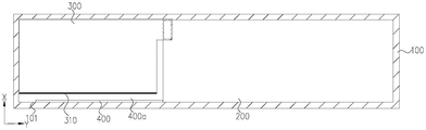
请参照图2,本申请实施例提供的一种电子设备1000至少包括壳体组件100、电路板组件200、电子组件300及天线组件400。Referring to FIG. 2 , an electronic device 1000 provided by an embodiment of the present application at least includes a housing component 100 , a circuit board component 200 , an electronic component 300 , and an antenna component 400 .
其中,壳体组件100包括但不限于为电子设备1000的外壳。该电子设备1000的外壳的至少部分的材质为非导电材质或者是对于电磁波的传输效率影响较小的材质。The housing assembly 100 includes, but is not limited to, a housing of the electronic device 1000 . The material of at least part of the casing of the electronic device 1000 is a non-conductive material or a material that has little effect on the transmission efficiency of electromagnetic waves.
壳体组件100具有壳体内腔,壳体内腔用于收容电路板组件200、电子组件300、天线组件400、摄像头组件、扬声器组件、麦克风组件、触摸板组件、显示屏组件等。The housing assembly 100 has a housing cavity for accommodating the circuit board assembly 200 , the electronic assembly 300 , the antenna assembly 400 , the camera assembly, the speaker assembly, the microphone assembly, the touch panel assembly, the display screen assembly, and the like.
所述电路板组件200设于所述壳体组件100内,即壳体组件100的壳体内腔中。可选的,电路板组件200为主板或者电路板组件200包括主板,主板亦可称为主机板、系统板、逻辑板等,主板上设有处理器等。可选的,主板为PCB多层板,包括多层介电层及设于介电层之间的金属导电层(例如铜箔层)。介电层用来保持线路及各层之间的绝缘性,俗称为基材。两层次以上的线路通过导电通孔彼此导通。金属导电层中至少一层作为电路板组件200的参考地层。本实施方式中,电路板组件200为硬质电路板,以设置射频芯片、板对板电连接器等。The circuit board assembly 200 is disposed in the casing assembly 100 , that is, in the casing cavity of the casing assembly 100 . Optionally, the circuit board assembly 200 is a motherboard or the circuit board assembly 200 includes a motherboard. The motherboard may also be referred to as a motherboard, a system board, a logic board, or the like, and a processor or the like is provided on the motherboard. Optionally, the main board is a multi-layer PCB, including multiple dielectric layers and a metal conductive layer (eg, a copper foil layer) disposed between the dielectric layers. The dielectric layer is used to maintain the insulation between the circuit and each layer, commonly known as the substrate. Lines on two or more levels are connected to each other through conductive vias. At least one of the metal conductive layers serves as a reference ground layer of the circuit board assembly 200 . In this embodiment, the circuit board assembly 200 is a rigid circuit board, and is provided with a radio frequency chip, a board-to-board electrical connector, and the like.
请参照图2,所述电子组件300设于所述壳体组件100内,即设于壳体组件100的壳体内腔中。所述电子组件300与所述电路板组件200相邻设置。所述电子组件300具有导电件310。所述导电件310用于电连接参考地。其中,所述导电件310所电连接的参考地包括但不限于为电路板组件200中的参考地层、或电子设备1000内部的其他参考地,例如,铝合金中框、其他电子器件的参考地等。具体的电连接方式包括但不限于通过板对板电连接、焊接、导电弹片等方式进行电连接。可选的,所述电子组件300包括但不限于为电池组件、摄像头组件、扬声器组件、麦克风组件、触摸板组件、显示屏组件等中的至少一者。Referring to FIG. 2 , the electronic component 300 is disposed in the casing assembly 100 , that is, disposed in the casing cavity of the casing assembly 100 . The electronic assembly 300 is disposed adjacent to the circuit board assembly 200 . The electronic component 300 has a conductive member 310 . The conductive member 310 is used for electrical connection to the reference ground. The reference ground to which the conductive member 310 is electrically connected includes, but is not limited to, the reference ground layer in the circuit board assembly 200 or other reference grounds inside the electronic device 1000 , for example, an aluminum alloy middle frame and reference grounds of other electronic devices Wait. Specific electrical connection methods include, but are not limited to, electrical connection through board-to-board electrical connection, welding, conductive elastic sheets, and the like. Optionally, the electronic assembly 300 includes, but is not limited to, at least one of a battery assembly, a camera assembly, a speaker assembly, a microphone assembly, a touch panel assembly, a display screen assembly, and the like.
本申请对于导电件310的形态不做具体的限定。导电件310的形态包括但不限于为嵌设的薄层状、表面的导电涂层、导电材质的支撑板、导电屏蔽罩等。本申请对于导电件310在电子组件300内的作用不做限定,可选的,导电件310包括但不限于为阻隔水、氧、遮光;或者,支撑作用;或者,防静电;或者,散热等。The present application does not specifically limit the form of the conductive member 310 . The form of the conductive member 310 includes, but is not limited to, an embedded thin layer, a conductive coating on the surface, a support plate made of conductive material, a conductive shield, and the like. The application does not limit the function of the conductive member 310 in the electronic assembly 300. Optionally, the conductive member 310 includes but is not limited to blocking water, oxygen, and shading; or, supporting; or, anti-static; or, heat dissipation, etc. .
举例而言,当所述电子组件300为电池组件时,电子组件300的导电件310为电池组件的铝塑膜中的铝层的一部分,或者为铝壳的一部分,用于阻隔水、氧、遮光等。当所述电子组件300为摄像头组件等设置导电材质的支撑罩时,电子组件300的导电件310为摄像头组件外周侧的导电材质的支撑罩的一部分,该支撑罩具有一定的刚性,用于防止外部的碰撞力或跌落应力传导至摄像头组件,影响摄像头组件内部的精密器件。For example, when the electronic component 300 is a battery component, the conductive member 310 of the electronic component 300 is a part of the aluminum layer in the aluminum-plastic film of the battery component, or a part of the aluminum shell for blocking water, oxygen, Shading, etc. When the electronic component 300 is a camera component and the like is provided with a support cover made of conductive material, the conductive member 310 of the electronic component 300 is a part of the support cover made of conductive material on the peripheral side of the camera component. The support cover has a certain rigidity to prevent External impact force or drop stress is transmitted to the camera assembly, affecting the precision components inside the camera assembly.
本申请中为了便于描述,以电子设备1000的电路板组件200的宽度方向定义为X轴方向,所述电子设备1000的电路板组件200的长度方向定义为Y轴方向,所述电子设备1000的电路板组件200的厚度方向定义为Z轴方向。其中,X轴方向、Y轴方向及Z轴方向两两垂直。其中,箭头所指示的方向为正向,箭头相反的方向为反向。In this application, for the convenience of description, the width direction of the circuit board assembly 200 of the electronic device 1000 is defined as the X-axis direction, and the length direction of the circuit board assembly 200 of the electronic device 1000 is defined as the Y-axis direction. The thickness direction of the circuit board assembly 200 is defined as the Z-axis direction. Among them, the X-axis direction, the Y-axis direction, and the Z-axis direction are perpendicular to each other. The direction indicated by the arrow is the forward direction, and the direction opposite to the arrow is the reverse direction.
可选的,所述电子组件300与电路板组件200沿Y轴方向排列。当然,在其他实施方式中,所述电子组件300与电路板组件200沿Y轴方向排列。壳体组件100在X-Y平面上围接于所述电路板组件200和电子组件300的周侧,壳体组件100还在Z轴方向上与电路板组件200、电子组件300相对设置。Optionally, the electronic assembly 300 and the circuit board assembly 200 are arranged along the Y-axis direction. Of course, in other embodiments, the electronic components 300 and the circuit board components 200 are arranged along the Y-axis direction. The housing assembly 100 surrounds the peripheral sides of the circuit board assembly 200 and the electronic assembly 300 on the X-Y plane, and the housing assembly 100 is also disposed opposite the circuit board assembly 200 and the electronic assembly 300 in the Z-axis direction.
请参照图2,所述导电件310与所述壳体组件100的预设内壁101相对且间隔设置。可选的,壳体组件100的预设内壁101为沿X轴正向朝向壳体内腔的内壁。换言之,所述电子组件300的朝向X轴反向的面与所述壳体组件100的预设内壁101相对且间隔设置。Referring to FIG. 2 , the conductive member 310 is opposite to and spaced apart from the predetermined inner wall 101 of the housing assembly 100 . Optionally, the predetermined inner wall 101 of the housing assembly 100 is an inner wall facing the inner cavity of the housing along the positive X-axis. In other words, the surface of the electronic component 300 opposite to the X axis is opposite to and spaced apart from the predetermined inner wall 101 of the housing component 100 .
所述天线组件400包括辐射体410。辐射体410设于所述导电件310与所述壳体组件100的预设内壁101之间。换言之,部分的天线组件400至少部分收容于所述电子组件300的朝向X轴反向的面与所述壳体组件100的预设内壁101之间。即电子组件300、部分的天线组件400、壳体组件100的预设内壁101依次沿X轴方向排列。如此,天线组件400未设于电路板组件200旁边,而是设于电子组件300与壳体组件100之间的间隙中。The antenna assembly 400 includes a radiator 410 . The radiator 410 is disposed between the conductive member 310 and the predetermined inner wall 101 of the housing assembly 100 . In other words, part of the antenna assembly 400 is at least partially accommodated between the surface of the electronic assembly 300 opposite to the X-axis and the predetermined inner wall 101 of the housing assembly 100 . That is, the electronic component 300 , a part of the antenna component 400 , and the predetermined inner wall 101 of the housing component 100 are sequentially arranged along the X-axis direction. In this way, the antenna assembly 400 is not disposed beside the circuit board assembly 200 , but is disposed in the gap between the electronic assembly 300 and the housing assembly 100 .
可选的,壳体组件100的预设内壁101的材质为非导电材质,以减小对于天线组件400所收发的电磁波信号的影响。当然,可选的,壳体组件100的全部可以为非导电材质,也可以是对应辐射体410的部分的材质为非导电材质,其他部分的材质为金属材质等。其中,非导电材质包括塑料材质、陶瓷材质、玻璃材质等。本实施例中,以壳体组件100的预设内壁101的材质为塑料材质为例。Optionally, the material of the predetermined inner wall 101 of the housing component 100 is a non-conductive material, so as to reduce the influence on the electromagnetic wave signal transmitted and received by the antenna component 400 . Of course, optionally, the entire housing assembly 100 may be made of a non-conductive material, or a part corresponding to the radiator 410 may be made of a non-conductive material, and the other parts may be made of a metal material or the like. The non-conductive materials include plastic materials, ceramic materials, glass materials, and the like. In this embodiment, the material of the predetermined inner wall 101 of the housing assembly 100 is taken as an example of a plastic material.
请参照图3,所述辐射体410与所述导电件310耦合。由于所述导电件310电连接参考地,故所述导电件310可作为天线组件400的地板,即天线地。辐射体410电连接馈源,及辐射体410与所述导电件310之间电磁耦合,形成天线回路。Referring to FIG. 3 , the radiator 410 is coupled with the conductive member 310 . Since the conductive member 310 is electrically connected to the reference ground, the conductive member 310 can serve as the floor of the antenna assembly 400 , that is, the antenna ground. The radiator 410 is electrically connected to the feed source, and the electromagnetic coupling between the radiator 410 and the conductive member 310 forms an antenna loop.
请参照图3,所述辐射体410电连接所述电路板组件200。可选的,所述电路板组件200上设有射频芯片(未标号)。所述射频芯片电连接天线组件400的馈电单元(后续会进行具体说明)。换言之,本申请所述的射频芯片、天线组件400、电子组件300的导电件310、及电路板组件200上的参考地层形成天线系统800。辐射体410在射频芯片的激励信号下收发电磁波信号。可选的,所述天线系统800的工作频段包括2.4GHz~2.5GHz。所述天线系统800所支持的信号类型包括但不限于为Wi-Fi信号、蓝牙信号等。Referring to FIG. 3 , the radiator 410 is electrically connected to the circuit board assembly 200 . Optionally, a radio frequency chip (not numbered) is provided on the circuit board assembly 200 . The radio frequency chip is electrically connected to the feeding unit of the antenna assembly 400 (which will be described in detail later). In other words, the radio frequency chip, the antenna assembly 400 , the conductive member 310 of the electronic assembly 300 , and the reference ground layer on the circuit board assembly 200 described in this application form the antenna system 800 . The radiator 410 transmits and receives electromagnetic wave signals under the excitation signal of the radio frequency chip. Optionally, the working frequency band of the antenna system 800 includes 2.4GHz-2.5GHz. Signal types supported by the antenna system 800 include, but are not limited to, Wi-Fi signals, Bluetooth signals, and the like.
本申请提供的电子设备1000,通过设计天线组件400的辐射体410位于电子组件300与壳体组件100的预设内壁101之间,将电子组件300的导电件310电连接参考地,及辐射体410与电子组件300的导电件310耦合;在位置设计上,通过将辐射体410设于电子组件300与壳体组件100之间的间隙中,辐射体410无需占据电路板组件200旁边的空间,如此壳体组件100可紧贴电路板组件200设置,以利于整体的小型化;在功能设计上,通过利用电子组件300自身的导电件310作为天线组件400的天线地,实现了电子组件300的导电件310的复用,利于实现天线的功能,以兼容天线性能和尺寸小型化。In the electronic device 1000 provided by the present application, by designing the radiator 410 of the antenna assembly 400 to be located between the electronic assembly 300 and the preset inner wall 101 of the housing assembly 100 , the conductive member 310 of the electronic assembly 300 is electrically connected to the reference ground and the radiator The radiator 410 is coupled with the conductive member 310 of the electronic component 300; in terms of position design, by arranging the radiator 410 in the gap between the electronic component 300 and the housing component 100, the radiator 410 does not need to occupy the space next to the circuit board component 200, In this way, the housing assembly 100 can be placed close to the circuit board assembly 200 to facilitate the overall miniaturization; in functional design, by using the conductive member 310 of the electronic assembly 300 itself as the antenna ground of the antenna assembly 400, the electronic assembly 300 is realized. The multiplexing of the conductive members 310 is beneficial to realize the function of the antenna, so as to be compatible with the performance and miniaturization of the antenna.
对于智能眼镜等可穿戴电子设备1000而言,由于电路板组件200、电子组件300一般安装于智能眼镜的镜腿上靠近于镜片的位置。镜腿的延伸方向为Y轴方向。而镜腿的截面空间极其有限,当电路板组件200安装于镜腿之后,由于电路板组件200需要设置一些芯片等,电路板组件200自身体积相对较大,为了减小镜腿局部截面尺寸,镜腿处的壳体组件100紧贴于电路板组件200的周侧设置,那么电路板组件200的周侧无多余的空间设置天线组件400。For the wearable electronic device 1000 such as smart glasses, the circuit board assembly 200 and the electronic assembly 300 are generally installed on the temples of the smart glasses at a position close to the lens. The extension direction of the temple is the Y-axis direction. The cross-sectional space of the temple is extremely limited. After the circuit board assembly 200 is installed on the temple, since the circuit board assembly 200 needs to be provided with some chips, etc., the circuit board assembly 200 itself is relatively large. In order to reduce the local cross-sectional size of the temple, The housing assembly 100 at the temple is disposed in close contact with the peripheral side of the circuit board assembly 200 , so there is no extra space on the peripheral side of the circuit board assembly 200 for the antenna assembly 400 to be disposed.
本申请中通过将天线组件400的辐射体410设于电子组件300与壳体组件100的内壁之间,使辐射体410无需占据电路板组件200周侧的空间,以实现镜腿的截面尺寸相对较小,同时,天线组件400还复用电子组件300自身的导电件310作为参考地,确保天线组件400即使远离电路板组件200的参考地层也能够形成天线回路,有效地进行天线信号收发。In this application, by disposing the radiator 410 of the antenna assembly 400 between the electronic assembly 300 and the inner wall of the housing assembly 100 , the radiator 410 does not need to occupy the space on the peripheral side of the circuit board assembly 200 , so that the cross-sectional dimensions of the temples are opposite to each other. At the same time, the antenna assembly 400 also reuses the conductive member 310 of the electronic assembly 300 itself as a reference ground to ensure that the antenna assembly 400 can form an antenna loop even if it is far away from the reference ground layer of the circuit board assembly 200 to effectively transmit and receive antenna signals.
可选的,请参照图4,所述电子组件300包括电池组件500。所述电池组件500的外壳包括金属体530。位于所述电池组件500的预设侧面501的所述金属体530形成所述导电件310。金属体530可为电池组件500的铝塑膜中的铝层的一部分,或者为铝壳的一部分,用于阻隔水、氧、遮光等。所述金属体530电连接所述电路板组件200的参考地层。Optionally, referring to FIG. 4 , the electronic assembly 300 includes a battery assembly 500 . The housing of the battery assembly 500 includes a metal body 530 . The metal body 530 located on the predetermined side surface 501 of the battery assembly 500 forms the conductive member 310 . The metal body 530 can be a part of the aluminum layer in the aluminum-plastic film of the battery assembly 500, or a part of the aluminum shell, and is used for blocking water, oxygen, light shielding, and the like. The metal body 530 is electrically connected to the reference ground layer of the circuit board assembly 200 .
通过将天线组件400的辐射体410设于电池组件500与壳体组件100的内壁之间,使天线组件400的辐射体410无需占据电路板组件200周侧的空间,壳体组件100可紧贴于电路板组件200设置,如此,实现壳体组件100在X-Z平面内的截面尺寸相对较小,同时,天线组件400还复用电池组件500外壳内原本用于阻隔水、氧、遮光等的金属体530作为参考地,确保天线组件400复用到电池组件500中的金属体530,即使远离电路板组件200的参考地层也能够形成天线回路,有效地进行天线信号收发。By arranging the radiator 410 of the antenna assembly 400 between the battery assembly 500 and the inner wall of the casing assembly 100 , the radiator 410 of the antenna assembly 400 does not need to occupy the space on the peripheral side of the circuit board assembly 200 , and the casing assembly 100 can be tightly attached It is arranged on the circuit board assembly 200, so that the cross-sectional size of the casing assembly 100 in the X-Z plane is relatively small, and at the same time, the antenna assembly 400 also reuses the metal originally used to block water, oxygen, shading, etc. in the casing of the battery assembly 500. The body 530 is used as a reference ground to ensure that the antenna assembly 400 is multiplexed to the metal body 530 in the battery assembly 500, and an antenna loop can be formed even if it is far away from the reference ground layer of the circuit board assembly 200, and antenna signals can be transmitted and received effectively.
当然,在其他实施方式中,电子组件300还可以为摄像头组件、麦克风组件、显示屏组件等,导电件310可以为摄像头组件的支撑罩、或麦克风组件的补强板、或显示屏组件背侧的支撑板等。以上的支撑罩、补强板、支撑板的材质皆为导电材质,通过电连接至电路板组件200的参考地层,以形成本申请中的天线组件400的参考地。以上的设计可以实现壳体组件100可紧贴于电路板组件200设置,如此,实现壳体组件100在X-Z平面内的截面尺寸相对较小,同时,天线组件400还复用摄像头组件原本用于抵抗外界冲击力的支撑罩、或复用麦克风组件原本用于提高柔性电路板的支撑强度的补强板、或复用显示屏组件背侧原本用于支撑显示屏组件内部的其他结构的支撑板作为参考地,确保天线组件400复用到上述电子组件300中的导电件310,即使远离电路板组件200的参考地层也能够形成天线回路,有效地进行天线信号收发。Of course, in other embodiments, the electronic assembly 300 may also be a camera assembly, a microphone assembly, a display screen assembly, etc., and the conductive member 310 may be a support cover of the camera assembly, or a reinforcing plate of the microphone assembly, or the back side of the display screen assembly support plate, etc. The above-mentioned supporting cover, reinforcing plate and supporting plate are all conductive materials, and are electrically connected to the reference ground layer of the circuit board assembly 200 to form the reference ground of the antenna assembly 400 in the present application. The above design can realize that the housing assembly 100 can be placed in close contact with the circuit board assembly 200, so that the cross-sectional size of the housing assembly 100 in the X-Z plane is relatively small, and at the same time, the antenna assembly 400 also reuses the camera assembly originally used for A support cover that resists external impact, or a reinforcing plate originally used to improve the support strength of the flexible circuit board by the multiplexed microphone assembly, or a support plate originally used to support other structures inside the display assembly on the backside of the multiplexed display assembly As a reference, it is ensured that the antenna assembly 400 is multiplexed with the conductive member 310 in the electronic assembly 300, so that an antenna loop can be formed even if it is far away from the reference ground layer of the circuit board assembly 200, and antenna signal transmission and reception can be effectively performed.
关于电池组件500的金属体530与电路板组件200的参考地层的电连接包括但不限于以下实施方式:The electrical connection between the metal body 530 of the battery assembly 500 and the reference ground layer of the circuit board assembly 200 includes but is not limited to the following embodiments:
请参照图5,所述电池组件500包括电池510及电连接所述电池510的第一电连接器520。电池510包括外壳(即上述的电池组件500的外壳)、保护电路及电芯。外壳用于封装电芯和保护板。电芯的极耳通过保护电路电连接至第一电连接器520。第一电连接器520设于外壳外。所述第一电连接器520电连接所述电池510的外壳内的金属体530。即第一电连接器520电连接所述导电件310。可选的,所述导电件310电连接于所述第一电连接器520的至少一个引脚,本申请定义该引脚为第一接地引脚521。Referring to FIG. 5 , the battery assembly 500 includes a battery 510 and a first electrical connector 520 electrically connected to the battery 510 . The battery 510 includes a casing (ie, the casing of the battery assembly 500 described above), a protection circuit and a battery cell. The case is used to encapsulate the cell and the protection board. The tabs of the battery cells are electrically connected to the first electrical connector 520 through the protection circuit. The first electrical connector 520 is disposed outside the casing. The first electrical connector 520 is electrically connected to the metal body 530 in the casing of the battery 510 . That is, the first electrical connector 520 is electrically connected to the conductive member 310 . Optionally, the conductive member 310 is electrically connected to at least one pin of the first electrical connector 520 , which is defined as the first ground pin 521 in the present application.
所述电路板组件200包括主板210及设于所述主板210上的第二电连接器220。所述第二电连接器220电连接所述参考地层222。可选的,第二电连接器220的至少一个引脚通过走线和导电过孔电连接主板210的参考地层222,本申请定义该引脚为第二接地引脚221。可选的,第一电连接器520和第二电连接器220为板对板电连接器,以便于电池组件500和电路板组件200单独制备及可拆卸组装。当然,在其他实施方式中,第一电连接器520和第二电连接器220还可以为分别插接接头与插接接口。The circuit board assembly 200 includes a main board 210 and a second electrical connector 220 disposed on the main board 210 . The second electrical connector 220 is electrically connected to the reference ground layer 222 . Optionally, at least one pin of the second electrical connector 220 is electrically connected to the reference ground layer 222 of the motherboard 210 through traces and conductive vias, and this pin is defined as the second ground pin 221 in this application. Optionally, the first electrical connector 520 and the second electrical connector 220 are board-to-board electrical connectors, so that the battery assembly 500 and the circuit board assembly 200 can be prepared separately and assembled detachably. Of course, in other embodiments, the first electrical connector 520 and the second electrical connector 220 may also be plug connectors and plug interfaces, respectively.
请参照图5,当第一电连接器520与第二电连接器220对接时,第一接地引脚521电连接第二接地引脚221。所述导电件310与所述参考地层222通过所述第一电连接器520和所述第二电连接器220电连接。即所述导电件310与所述参考地层222通过第一接地引脚521与第二接地引脚221的电连接而电连接。换言之,导电件310、第一接地引脚521、第二接地引脚221、电路板组件200的参考地层222依次电连接。Referring to FIG. 5 , when the first electrical connector 520 is docked with the second electrical connector 220 , the first ground pin 521 is electrically connected to the second ground pin 221 . The conductive member 310 is electrically connected to the reference ground layer 222 through the first electrical connector 520 and the second electrical connector 220 . That is, the conductive member 310 and the reference ground layer 222 are electrically connected through the electrical connection between the first ground pin 521 and the second ground pin 221 . In other words, the conductive member 310 , the first ground pin 521 , the second ground pin 221 , and the reference ground layer 222 of the circuit board assembly 200 are electrically connected in sequence.
本实施方式中,通过设置电池510的外壳内的金属体530接地,还可以有效地防止电池510内部的电化学反应收到外界的电流、静电等的影响,提高电池510的充放电效率和稳定性。In this embodiment, by setting the metal body 530 in the casing of the battery 510 to be grounded, the electrochemical reaction inside the battery 510 can also be effectively prevented from being affected by external current, static electricity, etc., and the charging and discharging efficiency and stability of the battery 510 can be improved. sex.
可选的,请参照图2,所述辐射体410与所述导电件310之间具有绝缘间隙400a。当辐射体410与所述导电件310沿X轴方向相对设置时,所述绝缘间隙400a在X轴方向上的尺寸大于或等于1mm。可选的,所述绝缘间隙400a在X轴方向上的尺寸小于1.5mm,例如所述绝缘间隙400a在X轴方向上的尺寸为1.06mm,但不限于此数据。可以理解的,该绝缘间隙400a可作为天线组件400的净空空间,以调节天线组件400具有适合的对地电容,减小电池组件500的导电件310对于天线组件400的辐射影响,提高天线系统800的天线效率。所述绝缘间隙400a在X轴方向上的尺寸大于或等于1mm,天线组件400具有相对较好的辐射效率。Optionally, please refer to FIG. 2 , there is an insulating gap 400 a between the radiator 410 and the conductive member 310 . When the radiator 410 and the conductive member 310 are disposed opposite to each other along the X-axis direction, the dimension of the insulating gap 400a in the X-axis direction is greater than or equal to 1 mm. Optionally, the size of the insulating gap 400a in the X-axis direction is less than 1.5 mm, for example, the size of the insulating gap 400a in the X-axis direction is 1.06 mm, but not limited to this data. It can be understood that the insulating gap 400a can be used as the clearance space of the antenna assembly 400 to adjust the antenna assembly 400 to have a suitable capacitance to ground, reduce the radiation effect of the conductive member 310 of the battery assembly 500 on the antenna assembly 400, and improve the antenna system 800. antenna efficiency. The dimension of the insulating gap 400a in the X-axis direction is greater than or equal to 1 mm, and the antenna assembly 400 has relatively good radiation efficiency.
以下结合附图对于天线组件400的辐射体410的成型方式进行具体的举例说明。In the following, a specific example will be given to illustrate the forming method of the radiator 410 of the antenna assembly 400 with reference to the accompanying drawings.
可选的,请参照图6,所述辐射体410所在面朝向所述壳体组件100的预设内壁101。可选的,辐射体410所在面大致平行或平行于所述壳体组件100的预设内壁101。Optionally, please refer to FIG. 6 , where the radiator 410 faces the predetermined inner wall 101 of the housing assembly 100 . Optionally, the surface where the radiator 410 is located is substantially parallel or parallel to the predetermined inner wall 101 of the housing assembly 100 .
举例而言,所述辐射体410的材质为金属材质。所述辐射体410所在面朝向所述壳体组件100的预设内壁101设置。For example, the material of the radiator 410 is a metal material. The surface where the radiator 410 is located faces the predetermined inner wall 101 of the housing assembly 100 .
本申请对于所述辐射体410的具体形状不做具体的限定。所述辐射体410的形状包括但不限于为直线、弯折线、曲线、局部加宽等。举例而言,所述辐射体410为直线型,所述辐射体410的长度方向为Y轴方向。所述辐射体410的长度尺寸接近1/4工作波长,所述工作波长为工作频段对应的介质波长。当所述天线组件400的工作频段为2.4GHz~2.5GHz时,所述辐射体410的长度尺寸接近23.4mm。本申请对于辐射体410的宽度(辐射体410的宽度方向为Z轴方向)不做具体的限定。理论上辐射体410的宽度越宽,辐射体410的容性匹配更强,以平衡辐射体410的感性匹配,因此,在电子设备1000所允许的范围内,设置辐射体410的宽度相对较大,例如,2.74mm,但不限于此数据。The present application does not specifically limit the specific shape of the radiator 410 . The shape of the radiator 410 includes, but is not limited to, a straight line, a bent line, a curved line, a local widening, and the like. For example, the radiator 410 is linear, and the length direction of the radiator 410 is the Y-axis direction. The length dimension of the radiator 410 is close to 1/4 of the working wavelength, and the working wavelength is the medium wavelength corresponding to the working frequency band. When the operating frequency band of the antenna assembly 400 is 2.4GHz-2.5GHz, the length dimension of the radiator 410 is close to 23.4mm. The present application does not specifically limit the width of the radiator 410 (the width direction of the radiator 410 is the Z-axis direction). In theory, the wider the width of the radiator 410 is, the stronger the capacitive matching of the radiator 410 is to balance the inductive matching of the radiator 410. Therefore, within the range allowed by the electronic device 1000, the width of the radiator 410 is relatively large. , for example, 2.74mm, but not limited to this data.
在第一种天线组件400的辐射体410的成型方式中,请参照图6,所述天线组件400还包括柔性承载板420。所述辐射体410成型于所述柔性承载板420。可选的,柔性承载板420设有多层柔性介电层,辐射体410为多层柔性介电层之间的导电层,例如铜箔层。柔性承载板420与辐射体410形成柔性印刷电路(FPC)天线。可选的,柔性印刷电路(FPC)天线的厚度为0.13mm,但不限于此数据。In the first method of forming the radiator 410 of the antenna assembly 400 , please refer to FIG. 6 , the antenna assembly 400 further includes a flexible carrier board 420 . The radiator 410 is formed on the flexible carrier board 420 . Optionally, the flexible carrier board 420 is provided with multiple flexible dielectric layers, and the radiator 410 is a conductive layer between the multiple flexible dielectric layers, such as a copper foil layer. The flexible carrier board 420 and the radiator 410 form a flexible printed circuit (FPC) antenna. Optionally, the thickness of the flexible printed circuit (FPC) antenna is 0.13mm, but not limited to this data.
在第二种天线组件400的辐射体410的成型方式中,请参照图7,所述辐射体410通过激光直接成型工艺、印刷直接成型工艺、柔性印刷技术、凹版印刷、旋涂和浸涂等工艺成型于所述壳体组件100的预设内壁101或其他支架表面。通过上述工艺将辐射体410直接集成在所述壳体组件100的预设内壁101或其他支架表面上,既可以减小天线的所需空间,并同时将总产品尺寸保持得较小,还可以适配具有异形曲折轮廓的三维结构。In the second molding method of the radiator 410 of the antenna assembly 400, please refer to FIG. 7, the radiator 410 is formed by laser direct molding process, printing direct molding process, flexographic printing technology, gravure printing, spin coating and dip coating, etc. The process is formed on the predetermined inner wall 101 of the housing assembly 100 or other support surfaces. Integrating the radiator 410 directly on the predetermined inner wall 101 of the housing assembly 100 or other support surfaces through the above process can not only reduce the space required for the antenna, but also keep the overall product size small, and also Fits three-dimensional structures with profiled zigzag profiles.
在第三种天线组件400的辐射体410的成型方式中,请参照图8,所述辐射体410自身具有一定的刚度,例如,辐射体410为金属片材,即金属片材天线。本实施方式提供的辐射体410无需设置承载板,可以批量生产,便于安装。In the third molding method of the radiator 410 of the antenna assembly 400, please refer to FIG. 8, the radiator 410 itself has a certain rigidity, for example, the radiator 410 is a metal sheet, that is, a metal sheet antenna. The radiator 410 provided in this embodiment does not need to be provided with a carrier plate, can be mass-produced, and is easy to install.
以下结合附图对于天线组件400的辐射体410的设置位置、设置方式进行具体的举例说明。Hereinafter, specific examples are given for the setting position and setting manner of the radiator 410 of the antenna assembly 400 with reference to the accompanying drawings.
可选的,所述天线组件400的辐射体410设于或贴合于所述壳体组件100的预设内壁101,并与所述壳体组件100的预设内壁101共形。Optionally, the radiator 410 of the antenna assembly 400 is disposed on or attached to the predetermined inner wall 101 of the housing assembly 100 , and conforms to the predetermined inner wall 101 of the housing assembly 100 .
可选的,天线组件400的辐射体410可通过粘接、直接成型等方式设于壳体组件100的预设内壁101上。其中,天线组件400的辐射体410包括但不限于为柔性印刷电路(FPC)天线、或通过激光直接成型工艺、印刷直接成型工艺、柔性印刷技术、凹版印刷、旋涂、浸涂等工艺成型的天线、金属片材天线等。Optionally, the radiator 410 of the antenna assembly 400 may be provided on the predetermined inner wall 101 of the housing assembly 100 by means of bonding, direct molding, or the like. Wherein, the radiator 410 of the antenna assembly 400 includes, but is not limited to, a flexible printed circuit (FPC) antenna, or an antenna formed by a laser direct molding process, a printing direct molding process, a flexographic printing technology, gravure printing, spin coating, dip coating, etc. Antennas, sheet metal antennas, etc.
所述天线组件400的辐射体410与所述壳体组件100的预设内壁101共形,是指天线组件400的辐射体410为极薄基材,其中,天线组件400的辐射体410会随着壳体组件100的预设内壁101的形状变化而变化,如此,天线组件400的辐射体410所占据的空间小,也能够利用壳体组件100的极窄空间,促进电子设备1000的小型化。The radiator 410 of the antenna assembly 400 is conformal to the predetermined inner wall 101 of the housing assembly 100 , which means that the radiator 410 of the antenna assembly 400 is an extremely thin substrate, wherein the radiator 410 of the antenna assembly 400 will follow the casing. The shape of the predetermined inner wall 101 of the body assembly 100 changes, so that the space occupied by the radiator 410 of the antenna assembly 400 is small, and the extremely narrow space of the housing assembly 100 can be utilized to promote the miniaturization of the electronic device 1000 .
本申请对于壳体组件100的预设内壁101的形状不做具体的限定。可选的,壳体组件100的预设内壁101的形状包括但不限于为平面状、弧面状或曲面状等。The present application does not specifically limit the shape of the predetermined inner wall 101 of the housing assembly 100 . Optionally, the shape of the predetermined inner wall 101 of the housing assembly 100 includes, but is not limited to, a plane shape, a curved surface shape, a curved surface shape, and the like.
通过将天线组件400的辐射体410设于或贴合于所述壳体组件100的预设内壁101上,如此,能够实现天线组件400的辐射体410与电池组件500之间的绝缘间隙400a最大,可以实现既满足天线系统800所需的净空空间,又实现电池组件500的预设侧面501与壳体组件100的预设内壁101之间的距离相对较小,进而实现电子设备1000的小型化。By arranging or attaching the radiator 410 of the antenna assembly 400 on the predetermined inner wall 101 of the housing assembly 100, in this way, the insulation gap 400a between the radiator 410 of the antenna assembly 400 and the battery assembly 500 can be maximized , the clearance space required by the antenna system 800 can be satisfied, and the distance between the preset side surface 501 of the battery assembly 500 and the preset inner wall 101 of the housing assembly 100 can be relatively small, thereby realizing the miniaturization of the electronic device 1000 .
当然,在其他实施方式中,所述天线组件400的辐射体410还可以设于所述壳体组件100的预设内壁101与电池组件500的预设内壁101之间的空间中。例如,天线组件400的辐射体410与电池组件500的预设侧面501之间形成第一绝缘间隙,天线组件400的辐射体410与壳体组件100的预设内壁101之间形成第二绝缘间隙。其中,第一绝缘间隙形成天线系统800的净空空间,第二绝缘间隙用于收容其他器件,或在电磁波的辐射路径上形成空气间隙,提高天线系统800的辐射性能。Of course, in other embodiments, the radiator 410 of the antenna assembly 400 may also be disposed in the space between the predetermined inner wall 101 of the housing assembly 100 and the predetermined inner wall 101 of the battery assembly 500 . For example, a first insulating gap is formed between the radiator 410 of the antenna assembly 400 and the preset side surface 501 of the battery assembly 500 , and a second insulating gap is formed between the radiator 410 of the antenna assembly 400 and the preset inner wall 101 of the housing assembly 100 . The first insulating gap forms a clear space for the antenna system 800 , and the second insulating gap is used for accommodating other devices, or forming an air gap on the radiation path of electromagnetic waves to improve the radiation performance of the antenna system 800 .
可选的,请参照图9,所述电子设备1000还包括介质支架700。所述介质支架700固定于壳体组件100。所述介质支架700设于所述绝缘间隙400a内,并支撑于所述辐射体410。所述介质支架700的介电常数较小而且很稳定,例如,2~3;所述介质支架700的介质损耗较小,例如,0.002左右,以减小天线信号在传输过程中的信号损耗。Optionally, please refer to FIG. 9 , the electronic device 1000 further includes a medium support 700 . The medium support 700 is fixed to the housing assembly 100 . The dielectric support 700 is disposed in the insulating gap 400 a and supported by the radiator 410 . The dielectric constant of the dielectric support 700 is small and stable, for example, 2-3; the dielectric loss of the dielectric support 700 is small, for example, about 0.002, so as to reduce the signal loss of the antenna signal during transmission.
本申请对于介质支架700的形状不做具体的限定。可选的,介质支架700的形状包括但不限于实心板状、网格状、多个支脚等。The present application does not specifically limit the shape of the medium support 700 . Optionally, the shape of the media support 700 includes, but is not limited to, a solid plate shape, a grid shape, a plurality of legs, and the like.
可选的,介质支架700在Z轴方向固定连接于壳体组件100,其固定连接的方式包括但不限于为一体成型、焊接、螺接、胶粘等方式。Optionally, the medium support 700 is fixedly connected to the housing assembly 100 in the Z-axis direction, and the fixed connection methods include, but are not limited to, integral molding, welding, screwing, gluing, and the like.
介质支架700朝向壳体组件100的预设内壁101的一侧支撑于辐射体410。可选的,辐射体410可通过粘接、直接成型等方式设于介质支架700上。辐射体410包括但不限于为柔性印刷电路(FPC)天线、或通过激光直接成型工艺、印刷直接成型工艺、柔性印刷技术、凹版印刷、旋涂、浸涂等工艺成型的天线、金属片材天线等。The side of the dielectric support 700 facing the predetermined inner wall 101 of the housing assembly 100 is supported on the radiator 410 . Optionally, the radiator 410 may be provided on the dielectric support 700 by means of bonding, direct molding, or the like. The radiator 410 includes, but is not limited to, a flexible printed circuit (FPC) antenna, or an antenna formed by a laser direct molding process, a printing direct molding process, a flexible printing technology, gravure printing, spin coating, dip coating and other processes, and a metal sheet antenna. Wait.
本实施例中,辐射体410与壳体组件100的预设内壁101可具有间隙或紧密贴合。In this embodiment, the radiator 410 and the predetermined inner wall 101 of the housing assembly 100 may have a gap or be closely attached.
可选的,介质支架700与电池组件500的预设侧面501之间可以紧密贴合或间隔设置。Optionally, the medium support 700 and the predetermined side surface 501 of the battery assembly 500 may be closely fitted or arranged at intervals.
本实施例通过设置介质支架700,通过将辐射体410通过粘接、直接成型等方式设于介质支架700上,再将介质支架700固定于壳体组件100上,可以提高辐射体410的安装效率,且防止辐射体410在安装于狭小缝隙内时受到破坏;此外,通过选择介电常数和介电损耗较小的介质支架700,以减小对于天线系统800的辐射效率的影响。In this embodiment, the dielectric support 700 is provided, the radiator 410 is disposed on the dielectric support 700 by bonding, direct molding, etc., and then the dielectric support 700 is fixed on the housing assembly 100, so that the installation efficiency of the radiator 410 can be improved. , and prevent the radiator 410 from being damaged when installed in a narrow gap; in addition, by selecting the dielectric support 700 with smaller dielectric constant and dielectric loss, the influence on the radiation efficiency of the antenna system 800 is reduced.
可选的,请参照图10,所述介质支架700与所述壳体组件100的预设内壁101为一体成型。Optionally, please refer to FIG. 10 , the medium support 700 is integrally formed with the predetermined inner wall 101 of the housing assembly 100 .
具体的,在加工所述壳体组件100时,通过注塑成型,将对应于电池组件500处的壳体组件100的内壁厚度大于对应于电路板组件200处的壳体组件100的内壁厚度。然后通过CNC工艺在对应于电池组件500处的壳体组件100的内壁处沿Y轴方向形成收容槽100a,该收容槽100a的至少一个开口朝向Z轴正向。该收容槽100a的X轴正向侧为介质支架700,该收容槽100a的X轴正向侧为壳体组件100的预设内壁101。该收容槽100a沿Y轴方向可贯穿或不贯穿。Specifically, when processing the case assembly 100 , through injection molding, the inner wall thickness of the case assembly 100 corresponding to the battery assembly 500 is greater than that of the case assembly 100 corresponding to the circuit board assembly 200 . Then, a receiving groove 100a is formed along the Y-axis direction at the inner wall of the case assembly 100 corresponding to the battery assembly 500 through a CNC process, and at least one opening of the receiving groove 100a faces the positive direction of the Z-axis. The positive side of the X-axis of the receiving groove 100 a is the medium support 700 , and the positive side of the X-axis of the receiving groove 100 a is the predetermined inner wall 101 of the housing assembly 100 . The receiving groove 100a may or may not penetrate along the Y-axis direction.
天线组件400的辐射体410可以为柔性印刷电路(FPC)天线,柔性印刷电路(FPC)天线的一端电连接于电路板组件200,所述柔性印刷电路(FPC)天线的一端收容于收容槽100a内。The radiator 410 of the antenna assembly 400 may be a flexible printed circuit (FPC) antenna, one end of the flexible printed circuit (FPC) antenna is electrically connected to the circuit board assembly 200, and one end of the flexible printed circuit (FPC) antenna is accommodated in the receiving slot 100a Inside.
通过在制备壳体组件100时,成型收容槽100a,以便于成型用于收容天线组件400的辐射体410的安装位,便于将天线组件400的辐射体410安装于壳体组件100的预设内壁101与电池组件500的预设侧面501之间。When the housing assembly 100 is prepared, the accommodating groove 100 a is formed so as to form the installation position for accommodating the radiator 410 of the antenna assembly 400 , so as to facilitate the installation of the radiator 410 of the antenna assembly 400 on the predetermined inner wall of the housing assembly 100 101 and the preset side surface 501 of the battery assembly 500 .
在其他实施方式中,所述介质支架700可以与所述壳体组件100的预设内壁101单独成型。例如介质支架700通过焊接、螺接、胶粘等方式固定连接于壳体组件100。所述辐射体410固定于所述介质支架700上,以随着所述介质支架700安装于壳体组件100内。In other embodiments, the media holder 700 may be formed separately from the predetermined inner wall 101 of the housing assembly 100 . For example, the dielectric support 700 is fixedly connected to the housing assembly 100 by welding, screwing, gluing, or the like. The radiator 410 is fixed on the dielectric support 700 to be installed in the housing assembly 100 along with the dielectric support 700 .
进一步地,请参照图11,所述介质支架700固定连接于所述壳体组件100。所述介质支架700背离所述辐射体410的一侧抵接于所述电池组件500的预设侧面501。换言之,所述介质支架700可以作为电池组件500的预设侧面501所在侧的定位墙。如此,介质支架700可实现同时定位电池组件500和辐射体410,提高电池组件500、介质支架700、天辐射体410在壳体内腔中的安装稳定性。Further, please refer to FIG. 11 , the medium support 700 is fixedly connected to the housing assembly 100 . The side of the dielectric support 700 facing away from the radiator 410 abuts against the predetermined side surface 501 of the battery assembly 500 . In other words, the medium support 700 may serve as a positioning wall on the side where the predetermined side surface 501 of the battery assembly 500 is located. In this way, the dielectric support 700 can simultaneously position the battery assembly 500 and the radiator 410 , thereby improving the installation stability of the battery assembly 500 , the dielectric support 700 , and the radiator 410 in the inner cavity of the housing.
请参照图12,所述电子设备1000还包括可压缩缓冲件600。所述可压缩缓冲件600设于所述电池组件500的预设侧面501与所述介质支架700之间。所述可压缩缓冲件600用于为电池组件500的安装提供一定的可活动空间。可选的,可压缩缓冲件600包括但不限于为弹性硅胶、泡棉等。当电池组件500安装于介质支架700朝向X正向所在侧时,可压缩缓冲件600被压缩,且可压缩缓冲件600还具有一定的可压缩余量。Referring to FIG. 12 , the electronic device 1000 further includes a compressible buffer 600 . The compressible buffer 600 is disposed between the predetermined side surface 501 of the battery assembly 500 and the medium support 700 . The compressible buffer 600 is used to provide a certain movable space for the installation of the battery assembly 500 . Optionally, the compressible buffer member 600 includes, but is not limited to, elastic silicone, foam, and the like. When the battery assembly 500 is installed on the side where the media support 700 faces the positive X direction, the compressible buffer member 600 is compressed, and the compressible buffer member 600 also has a certain compressibility margin.
可选的,请参照图13,所述导电件310包括沿所述电池组件500的厚度方向(Z轴方向)依次连接的第一弧形面311、中间侧面312及第二弧形面313。所述中间侧面312平行或大致平行于壳体组件100的预设内壁101。所述辐射体410与导电件310相对设置,包括但不限于以下的实施方式:第一种实施方式中,所述辐射体410与所述中间侧面312相对设置。可选的,所述中间侧面312为中间平直侧面,辐射体410与电池组件500的中间平直侧面相对设置。或者,第二种实施方式中,所述辐射体410的至少部分与所述第一弧形面311相对设置;或者,第三种实施方式中,所述辐射体410的至少部分与所述第二弧形面313相对设置。辐射体410还能够上移与第一弧形面311相对,或下移与第二弧形面313相对,以在不增加电池组件500的预设侧面501与壳体组件100的预设内壁101之间的距离的同时增加天线组件400的净空空间,进而增加天线系统800的天线性能。Optionally, please refer to FIG. 13 , the conductive member 310 includes a first arc-shaped surface 311 , a middle side surface 312 and a second arc-shaped surface 313 connected in sequence along the thickness direction (Z-axis direction) of the battery assembly 500 . The middle side surface 312 is parallel or substantially parallel to the predetermined inner wall 101 of the housing assembly 100 . The radiator 410 is disposed opposite to the conductive member 310 , including but not limited to the following embodiments: In the first embodiment, the radiator 410 is disposed opposite to the middle side surface 312 . Optionally, the middle side surface 312 is a middle flat side surface, and the radiator 410 is disposed opposite to the middle flat side surface of the battery assembly 500 . Alternatively, in the second embodiment, at least part of the radiator 410 is disposed opposite to the first arc-shaped surface 311 ; or, in the third embodiment, at least part of the radiator 410 is opposite to the first arc surface 311 ; The two arc-shaped surfaces 313 are opposite to each other. The radiator 410 can also be moved up to face the first arc-shaped surface 311 , or moved down to face the second arc-shaped face 313 , so as to not increase the preset side surface 501 of the battery assembly 500 and the preset inner wall 101 of the housing assembly 100 The distance between them increases the headroom of the antenna assembly 400 , thereby increasing the antenna performance of the antenna system 800 .
举例而言,所述电池组件500沿Z轴方向的厚度为6.7mm,所述中间侧面312沿Z轴方向的厚度为2.7mm。辐射体410沿Z轴方向的厚度为2.7mm。故可设置辐射体410与所述中间侧面312平行且正对,也可以设置辐射体410沿Z轴方向与所述中间侧面312相错开,辐射体410的一部分正对于所述中间侧面312,辐射体410的另一部分正对于电池组件500的第一弧形面311,或者,辐射体410的一部分正对于所述中间侧面312,辐射体410的另一部分正对于电池组件500的第二弧形面313。For example, the thickness of the battery assembly 500 along the Z-axis direction is 6.7 mm, and the thickness of the middle side surface 312 along the Z-axis direction is 2.7 mm. The thickness of the radiator 410 in the Z-axis direction is 2.7 mm. Therefore, the radiator 410 can be set to be parallel to the middle side surface 312 and face each other, or the radiator 410 can be set to be staggered from the middle side surface 312 along the Z-axis direction, and a part of the radiator 410 is facing the middle side surface 312. Another part of the body 410 is facing the first arc surface 311 of the battery assembly 500 , or, a part of the radiator 410 is facing the middle side surface 312 , and another part of the radiator 410 is facing the second arc surface of the battery assembly 500 313.
以下结合附图对于本申请实施例提供的电路板组件200、电池组件500及天线组件400的排布关系进行说明。The arrangement relationship of the circuit board assembly 200 , the battery assembly 500 , and the antenna assembly 400 provided by the embodiments of the present application will be described below with reference to the accompanying drawings.
请参照图14,所述电路板组件200与所述电池组件500沿第一方向排列。所述电池组件500与所述天线组件400的辐射体410沿第二方向排列。所述第二方向与所述第一方向垂直。其中,所述第一方向为Y轴方向。所述第二方向为X轴方向。Referring to FIG. 14 , the circuit board assembly 200 and the battery assembly 500 are arranged along a first direction. The battery assembly 500 and the radiator 410 of the antenna assembly 400 are arranged along the second direction. The second direction is perpendicular to the first direction. Wherein, the first direction is the Y-axis direction. The second direction is the X-axis direction.
进一步地,请参照图14,在X-Y平面内,壳体组件100包括相对设置的第一内壁110和第二内壁120。第一内壁110、第二内壁120皆沿Y轴方向延伸。所述第一内壁110的一部分和所述第二内壁120的一部分分别设于所述电路板组件200的相对两侧。第一内壁110的另一部分和第二内壁120的另一部分分别设于电池组件500的相对两侧。所述电池组件500的第三侧与所述电路板组件200的第三侧相邻设置。第一内壁110的另一部分即为上述的预设内壁101。天线组件400的辐射体410设于所述第一内壁110的另一部分与电路板组件200之间。Further, please refer to FIG. 14 , in the X-Y plane, the housing assembly 100 includes a first inner wall 110 and a second inner wall 120 which are disposed opposite to each other. The first inner wall 110 and the second inner wall 120 both extend along the Y-axis direction. A portion of the first inner wall 110 and a portion of the second inner wall 120 are respectively disposed on opposite sides of the circuit board assembly 200 . Another part of the first inner wall 110 and another part of the second inner wall 120 are respectively disposed on opposite sides of the battery assembly 500 . The third side of the battery assembly 500 is disposed adjacent to the third side of the circuit board assembly 200 . Another part of the first inner wall 110 is the above-mentioned predetermined inner wall 101 . The radiator 410 of the antenna assembly 400 is disposed between another part of the first inner wall 110 and the circuit board assembly 200 .
可选的,请参照图14,壳体组件100还包括连接在所述第一内壁110与所述第二内壁120之间的第三内壁130及第四内壁140,第三内壁130和第四内壁140皆沿X轴方向延伸。所述第三内壁130设于所述电路板组件200的第四侧。第四内壁140设于所述电池组件500的第四侧。当然,在其他的实施方式中,所述电路板组件200的第四侧、所述电池组件500的第四侧分别与其他的器件相邻,故未在所述电路板组件200的第四侧、所述电池组件500的第四侧设置第三内壁130和第四内壁140。Optionally, please refer to FIG. 14 , the housing assembly 100 further includes a third inner wall 130 and a fourth inner wall 140 connected between the first inner wall 110 and the second inner wall 120 , the third inner wall 130 and the fourth inner wall 140 The inner walls 140 all extend along the X-axis direction. The third inner wall 130 is disposed on the fourth side of the circuit board assembly 200 . The fourth inner wall 140 is disposed on the fourth side of the battery assembly 500 . Of course, in other embodiments, the fourth side of the circuit board assembly 200 and the fourth side of the battery assembly 500 are adjacent to other devices respectively, so they are not on the fourth side of the circuit board assembly 200 . . The fourth side of the battery assembly 500 is provided with a third inner wall 130 and a fourth inner wall 140 .
本实施例通过设计电路板组件200与电池组件500沿Y轴方向设置,且天线组件400的辐射体410设于电路板组件200沿X轴方向的一侧,如此,天线组件400的辐射体410无需占据电路板组件200X轴侧的空间,而是利用电池组件500X轴侧的空间,如此,壳体组件100的第一内壁110和第二内壁120可以紧贴电路板组件200设置,进而实现壳体组件100在X-Z平面内的截面尺寸相对较小,促进电子设备1000的小型化。In this embodiment, the circuit board assembly 200 and the battery assembly 500 are designed to be disposed along the Y-axis direction, and the radiator 410 of the antenna assembly 400 is disposed on one side of the circuit board assembly 200 along the X-axis direction. In this way, the radiator 410 of the antenna assembly 400 Instead of occupying the space on the 200X axis side of the circuit board assembly, the space on the 500X axis side of the battery assembly is used. In this way, the first inner wall 110 and the second inner wall 120 of the casing assembly 100 can be placed in close contact with the circuit board assembly 200, thereby realizing a casing The cross-sectional dimension of the body assembly 100 in the X-Z plane is relatively small, facilitating miniaturization of the electronic device 1000 .
以下以天线组件400的辐射体410为柔性印刷电路(FPC)天线为例对天线组件400的辐射体410与电路板组件200的连接方式进行举例说明。Hereinafter, the connection manner of the radiator 410 of the antenna assembly 400 and the circuit board assembly 200 will be illustrated by taking the radiator 410 of the antenna assembly 400 as an example of a flexible printed circuit (FPC) antenna.
可选的,请参照图15~图17,所述柔性承载板420包括相连接的连接部423及承载部421。所述连接部423沿所述第二方向延伸。所述连接部423用于承载电连接所述电路板组件200的馈电单元430。所述承载部421沿所述第一方向延伸。所述承载部421用于承载所述辐射体410。所述承载部421与所述壳体组件100的预设内壁101相对设置。Optionally, please refer to FIG. 15 to FIG. 17 , the flexible carrying board 420 includes a connecting portion 423 and a carrying portion 421 which are connected to each other. The connecting portion 423 extends along the second direction. The connecting portion 423 is used to carry the feeding unit 430 electrically connected to the circuit board assembly 200 . The bearing portion 421 extends along the first direction. The carrying portion 421 is used to carry the radiator 410 . The bearing portion 421 is disposed opposite to the predetermined inner wall 101 of the housing assembly 100 .
其中,第一方向为Y轴方向。第二方向为X轴方向。换言之,所述连接部423与所述承载部421的延伸方向不同。可选的,柔性承载板420可以为直线形的柔性板,将直线形的柔性板依次弯折呈沿X轴方向延伸的连接部423和沿Y轴方向延伸的承载部421。再可选的,柔性承载板420可以呈L型,其中,L型的柔性承载板420沿Y轴方向延伸的部分为承载部421,L型的柔性承载板420沿X轴方向延伸的部分为连接部423。The first direction is the Y-axis direction. The second direction is the X-axis direction. In other words, the extending directions of the connecting portion 423 and the bearing portion 421 are different. Optionally, the flexible bearing board 420 may be a linear flexible board, and the linear flexible board is sequentially bent to form a connecting portion 423 extending along the X-axis direction and a bearing portion 421 extending along the Y-axis direction. Alternatively, the flexible bearing board 420 may be in an L-shape, wherein the portion of the L-shaped flexible bearing board 420 extending along the Y-axis direction is the bearing portion 421 , and the portion of the L-shaped flexible bearing board 420 extending along the X-axis direction is the bearing portion 421 . Connection part 423 .
可选的,请参照图15,所述电路板组件200包括相背设置的第一承载面201和第二承载面202(第二承载面202位于第一承载面201的背面,用虚线指示),以及连接于所述第一承载面201和第二承载面202的第一周侧面203,所述第一承载面201朝向Z轴正向,第二承载面202朝向Z轴反向。第一周侧面203朝向Y轴反向,即朝向电池组件500所在侧。所述第一承载面201和第二承载面202皆用于承载电子器件。Optionally, please refer to FIG. 15 , the circuit board assembly 200 includes a first bearing surface 201 and a second bearing surface 202 arranged opposite to each other (the second bearing surface 202 is located on the back of the first bearing surface 201 , indicated by a dotted line) , and the first peripheral side surface 203 connected to the first bearing surface 201 and the second bearing surface 202 , the first bearing surface 201 faces the positive direction of the Z axis, and the second bearing surface 202 faces the reverse direction of the Z axis. The first circumferential side surface 203 is opposite to the Y axis, that is, toward the side where the battery assembly 500 is located. Both the first carrying surface 201 and the second carrying surface 202 are used for carrying electronic devices.
其中,所述连接部423与所述电路板组件200相对设置包括但不限于以下的实施方式:Wherein, the connection portion 423 is disposed opposite to the circuit board assembly 200 including but not limited to the following embodiments:
第一种实施方式中,请参照图15,所述连接部423与所述第二承载面202相对设置。具体的,第二承载面202上设有电连接射频芯片240的射频端口,所述连接部423上的馈电单元430与射频端口电连接。所述承载部421与所述壳体组件100的预设内壁101相对设置。柔性承载板420的承载部421及辐射体410设于所述收容槽100a内。柔性承载板420呈L型。连接部423从所述收容槽100a朝向Z轴正方向的开口伸出后弯折180°后朝向Z轴反向延伸,再弯折90°朝向X轴正向延伸,并与所述第二承载面202相对设置,实现馈电单元430与电路板组件200上的射频端口电连接及天线组件400占据的空间小。In the first embodiment, please refer to FIG. 15 , the connecting portion 423 is disposed opposite to the second bearing surface 202 . Specifically, the second bearing surface 202 is provided with a radio frequency port that is electrically connected to the radio frequency chip 240 , and the power feeding unit 430 on the connection portion 423 is electrically connected to the radio frequency port. The bearing portion 421 is disposed opposite to the predetermined inner wall 101 of the housing assembly 100 . The carrying portion 421 of the flexible carrying board 420 and the radiator 410 are disposed in the receiving groove 100a. The flexible carrier board 420 is L-shaped. The connecting portion 423 protrudes from the opening of the receiving groove 100a toward the positive direction of the Z-axis, bends 180°, then extends in the reverse direction of the Z-axis, and then bends 90° to extend toward the positive direction of the X-axis, and is connected with the second bearing. The surfaces 202 are disposed opposite to each other, so that the power feeding unit 430 is electrically connected to the radio frequency port on the circuit board assembly 200 and the space occupied by the antenna assembly 400 is small.
第二种实施方式中,请参照图16,所述连接部423与所述第一承载面201相对设置。具体的,第一承载面201上设有电连接射频芯片240的射频端口,所述连接部423上的馈电单元430与射频端口电连接。所述承载部421与所述壳体组件100的预设内壁101相对设置。柔性承载板420的承载部421及辐射体410设于所述收容槽100a内。柔性承载板420呈L型。连接部423从所述收容槽100a朝向Z轴正方向的开口伸出后弯折90°后与所述第一承载面201相对设置,实现馈电单元430与电路板组件200上的射频端口电连接及天线组件400占据的空间小。In the second embodiment, please refer to FIG. 16 , the connecting portion 423 is disposed opposite to the first bearing surface 201 . Specifically, the first bearing surface 201 is provided with a radio frequency port that is electrically connected to the radio frequency chip 240 , and the power feeding unit 430 on the connecting portion 423 is electrically connected to the radio frequency port. The bearing portion 421 is disposed opposite to the predetermined inner wall 101 of the housing assembly 100 . The carrying portion 421 of the flexible carrying board 420 and the radiator 410 are disposed in the receiving groove 100a. The flexible carrier board 420 is L-shaped. The connecting portion 423 protrudes from the opening of the receiving slot 100a toward the positive direction of the Z-axis, is bent at 90°, and is positioned opposite to the first bearing surface 201, so that the power feeding unit 430 is electrically connected to the RF port on the circuit board assembly 200. The connection and antenna assembly 400 takes up little space.
第三种实施方式中,请参照图17,所述连接部423与所述第一周侧面203相对设置。具体的,第一周侧面203上设有电连接射频芯片240的射频端口,所述连接部423上的馈电单元430与射频端口电连接。所述承载部421与所述壳体组件100的预设内壁101相对设置,所述收容槽100a可设有朝向Y轴正方向的开口,如此,实现柔性承载板420的承载部421及辐射体410设于所述收容槽100a内。柔性承载板420为直线型。连接部423从所述收容槽100a朝向Y轴正方向的开口伸出后弯折90°后与所述第一周侧面203相对设置,实现馈电单元430与电路板组件200上的射频端口电连接及天线组件400占据的空间小。In the third embodiment, please refer to FIG. 17 , the connecting portion 423 is disposed opposite to the first peripheral side surface 203 . Specifically, the first peripheral side surface 203 is provided with a radio frequency port electrically connected to the radio frequency chip 240 , and the power feeding unit 430 on the connecting portion 423 is electrically connected to the radio frequency port. The carrying portion 421 is disposed opposite to the predetermined inner wall 101 of the housing assembly 100 , and the receiving slot 100 a may be provided with an opening facing the positive direction of the Y-axis. In this way, the carrying portion 421 and the radiator of the flexible carrying board 420 are realized. 410 is disposed in the receiving groove 100a. The flexible carrier plate 420 is straight. The connecting portion 423 protrudes from the opening of the receiving slot 100a toward the positive direction of the Y-axis, is bent at 90°, and is positioned opposite to the first peripheral side surface 203, so that the power feeding unit 430 can be electrically connected to the RF port on the circuit board assembly 200. The connection and antenna assembly 400 takes up little space.
所述电路板组件200包括主板210及设于主板210上的射频芯片240、射频端口等电子器件。故上述所述电路板组件200的第一承载面201、第二承载面202、第一周侧面203也是主板210的第一承载面201、第二承载面202、第一周侧面203。The circuit board assembly 200 includes a main board 210 and electronic devices such as a radio frequency chip 240 and a radio frequency port disposed on the main board 210 . Therefore, the first bearing surface 201 , the second bearing surface 202 , and the first peripheral side surface 203 of the circuit board assembly 200 are also the first bearing surface 201 , the second bearing surface 202 , and the first peripheral side surface 203 of the motherboard 210 .
本实施方式中,请参照图15及图16,所述连接部423与所述主板210沿厚度方向相对设置。换言之,所述连接部423与所述主板210的第一承载面201或第二承载面202相对设置。In this embodiment, please refer to FIG. 15 and FIG. 16 , the connecting portion 423 and the main board 210 are disposed opposite to each other along the thickness direction. In other words, the connecting portion 423 is disposed opposite to the first bearing surface 201 or the second bearing surface 202 of the motherboard 210 .
进一步地,请参照图18及图19,所述连接部423与所述第二承载面202相对设置。所述承载部421从所述第一承载面201的朝向方向安装于所述壳体组件100的预设内壁101与所述电池组件500的预设侧面501之间。即收容槽100a的开口朝向与所述第一承载面201的朝向方向相同。所述承载部421与所述壳体组件100的预设内壁101相对设置。柔性承载板420的承载部421及辐射体410设于所述收容槽100a内。柔性承载板420呈L型。所述柔性承载板420还包括连接在所述连接部423与所述承载部421之间的弯折部422。弯折部422从所述收容槽100a朝向Z轴正方向的开口伸出后弯折180°后朝向Z轴反向延伸,再弯折90°,直至所述连接部423朝向X轴正向延伸,与所述第二承载面202相对设置,实现馈电单元430与电路板组件200上的射频端口电连接及天线组件400占据的空间小。Further, please refer to FIG. 18 and FIG. 19 , the connecting portion 423 is disposed opposite to the second bearing surface 202 . The bearing portion 421 is installed between the predetermined inner wall 101 of the housing assembly 100 and the predetermined side surface 501 of the battery assembly 500 from the facing direction of the first bearing surface 201 . That is, the opening direction of the receiving groove 100 a is the same as the direction of the first bearing surface 201 . The bearing portion 421 is disposed opposite to the predetermined inner wall 101 of the housing assembly 100 . The carrying portion 421 of the flexible carrying board 420 and the radiator 410 are disposed in the receiving groove 100a. The flexible carrier board 420 is L-shaped. The flexible carrying board 420 further includes a bending portion 422 connected between the connecting portion 423 and the carrying portion 421 . The bent portion 422 protrudes from the opening of the receiving groove 100a toward the positive direction of the Z-axis, bends 180°, then extends in the reverse direction of the Z-axis, and then bends 90° until the connecting portion 423 extends toward the positive direction of the X-axis , is disposed opposite to the second bearing surface 202 , so that the power feeding unit 430 is electrically connected to the radio frequency port on the circuit board assembly 200 and the space occupied by the antenna assembly 400 is small.
当所述壳体组件100的预设内壁101与所述电池组件500的预设侧面501之间设有用于支撑所述承载部421的介质支架700时,所述弯折部422沿所述主板210的侧面与所述介质支架700之间的间隙绕过所述介质支架700,并连接所述承载部421。When a medium support 700 for supporting the carrying portion 421 is provided between the predetermined inner wall 101 of the housing assembly 100 and the predetermined side surface 501 of the battery assembly 500 , the bent portion 422 is formed along the main board. The gap between the side surface of 210 and the media support 700 bypasses the media support 700 and is connected to the bearing portion 421 .
请参照图15及图16,所述天线组件400还包括至少一个馈电单元430。所述至少一个馈电单元430设于所述连接部423。所述馈电单元430电连接所述辐射体410与所述主板210上的射频端口;和/或,所述馈电单元430电连接所述辐射体410与所述主板210的参考地层222。Referring to FIG. 15 and FIG. 16 , the antenna assembly 400 further includes at least one feeding unit 430 . The at least one feeding unit 430 is provided on the connecting portion 423 . The feeding unit 430 is electrically connected to the radiator 410 and the radio frequency port on the mainboard 210 ; and/or the feeding unit 430 is electrically connected to the radiator 410 and the reference ground layer 222 of the mainboard 210 .
换言之,本申请中的天线组件400可以为单馈点方案,也可以用到双馈电点方案。单馈电点方案的辐射性能会略优于双馈电点方案约0.5dB。In other words, the antenna assembly 400 in the present application may be a single feed point scheme or a dual feed point scheme. The radiation performance of the single feed point scheme is slightly better than that of the double feed point scheme by about 0.5dB.
可选的,当馈电单元430的数量为一个时,所述馈电单元430电连接所述辐射体410与所述主板210上的射频端口。Optionally, when the number of feeding units 430 is one, the feeding unit 430 is electrically connected to the radiator 410 and the radio frequency port on the main board 210 .
当馈电单元430的数量为两个时,一个所述馈电单元430电连接所述辐射体410与所述主板210上的射频端口,另一个所述馈电单元430电连接所述辐射体410与所述主板210的参考地层222。When the number of feed units 430 is two, one of the feed units 430 is electrically connected to the radiator 410 and the radio frequency port on the motherboard 210 , and the other of the feed units 430 is electrically connected to the radiator 410 and the reference ground 222 of the motherboard 210 .
请参照图19,所述电路板组件200还包括至少一个导电弹片230。导电弹片230的数量与馈电单元430的数量相同。当导电弹片230的数量为一个时,所述导电弹片230的一端弹性抵接并电连接所述馈电单元430,所述导电弹片230的另一端固定于所述主板210并电连接所述主板210上的射频端口。通过馈电单元430与主板210上的导电弹片230压接,实现天线馈电。Referring to FIG. 19 , the circuit board assembly 200 further includes at least one conductive elastic piece 230 . The number of the conductive elastic pieces 230 is the same as the number of the feeding units 430 . When the number of conductive elastic sheets 230 is one, one end of the conductive elastic sheet 230 elastically abuts against and is electrically connected to the feeding unit 430, and the other end of the conductive elastic sheet 230 is fixed to the main board 210 and electrically connected to the main board RF port on 210. The antenna feeding is realized by crimping the feeding unit 430 with the conductive elastic sheet 230 on the main board 210 .
当导电弹片230的数量为两个时,一个所述导电弹片230的一端弹性抵接并电连接一个所述馈电单元430,一个所述导电弹片230的另一端固定于所述主板210并电连接所述主板210上的射频端口。另一个所述导电弹片230的一端弹性抵接并电连接另一个所述馈电单元430,另一个所述导电弹片230的另一端固定于所述主板210并电连接所述主板210的参考地层222。通过馈电单元430与主板210上的导电弹片230压接,实现天线馈电。When the number of conductive elastic sheets 230 is two, one end of one conductive elastic sheet 230 elastically abuts and electrically connects to one of the feeding units 430, and the other end of one conductive elastic sheet 230 is fixed to the main board 210 and electrically connected Connect to the radio frequency port on the motherboard 210 . One end of the other conductive elastic sheet 230 elastically contacts and is electrically connected to the other feeding unit 430 , and the other end of the other conductive elastic sheet 230 is fixed to the main board 210 and is electrically connected to the reference ground layer of the main board 210 . 222. The antenna feeding is realized by crimping the feeding unit 430 with the conductive elastic sheet 230 on the main board 210 .
请参照图19,所述天线组件400还包括补强板440。所述补强板440设于所述连接部423且位于背离所述馈电单元430的一侧。可选的,补强板440的材质为PI材料,补强板440的厚度约为0.3mm。补强板440为连接部423处提供一定的刚度,以保障馈电单元430与导电弹片230之间的连接可靠性。Referring to FIG. 19 , the antenna assembly 400 further includes a reinforcing plate 440 . The reinforcing plate 440 is disposed on the connecting portion 423 and is located on a side away from the power feeding unit 430 . Optionally, the material of the reinforcing plate 440 is PI material, and the thickness of the reinforcing plate 440 is about 0.3 mm. The reinforcing plate 440 provides a certain rigidity for the connecting portion 423 to ensure the reliability of the connection between the feeding unit 430 and the conductive elastic sheet 230 .
下表1是天线组件400收发Wi-Fi频段的空中下载技术测试(Over The Air,OTA)测试数据。OTA测试是整机辐射性能方面的测试。表1中,测试项802.11B的传导功率在15dBm左右,灵敏度在-85dBm左右。TRP全称为Total Radiated Power,即总辐射功率。是电子设备1000整机在空间三维球面上的射频辐射功率的积分值,反应了电子设备1000在所有方向上的发射特性。TIS(Total Isotropic Sensitivity):反映在整个辐射球面电子设备1000接收灵敏度指标的情况。它反映了电子设备1000整机的接收灵敏度情况,跟电子设备1000的传导灵敏度和天线的辐射性能有关。Table 1 below is the test data of the Over The Air (OTA) technology test for the antenna assembly 400 to transmit and receive the Wi-Fi frequency band. The OTA test is a test of the radiation performance of the whole machine. In Table 1, the conducted power of the test item 802.11B is about 15dBm, and the sensitivity is about -85dBm. The full name of TRP is Total Radiated Power, that is, the total radiated power. It is the integral value of the radio frequency radiation power of the electronic device 1000 on the three-dimensional spherical surface in space, and reflects the emission characteristics of the electronic device 1000 in all directions. TIS (Total Isotropic Sensitivity): reflects the condition of the receiving sensitivity index of the entire radiating spherical electronic device 1000 . It reflects the receiving sensitivity of the electronic device 1000 as a whole, and is related to the conduction sensitivity of the electronic device 1000 and the radiation performance of the antenna.
从表1中1信道、7信道、11信道的辐射功率分别为11dBm、11.2dBm、12.0dBm可以看出,整机的天线效率大于或等于-4dB,常规的可穿戴内置天线在wi-fi2.4G频段的天线效率性能平均在-5dB左右,故本申请的天线效率大于或等于-4dB,这反映了相较于常规更好的天线性能。其中,天线效率为辐射功率与传导功率之差。从7信道的灵敏度结果可以看出,全向接收灵敏度接近于-85dBm,说明本申请提供的电子设备1000的全向接收灵敏度相对较高。此外,当电子设备1000是具有显示屏的产品时,在亮屏和灭屏的情况下,电子设备1000皆能够保持相对较高的全向接收灵敏度。From Table 1, the radiated power of channel 1, channel 7, and channel 11 are 11dBm, 11.2dBm, and 12.0dBm, respectively. It can be seen that the antenna efficiency of the whole machine is greater than or equal to -4dB. The antenna efficiency performance of the 4G frequency band is about -5dB on average, so the antenna efficiency of the present application is greater than or equal to -4dB, which reflects better antenna performance than conventional ones. where the antenna efficiency is the difference between the radiated power and the conducted power. It can be seen from the sensitivity results of the 7 channels that the omnidirectional receiving sensitivity is close to -85dBm, indicating that the omnidirectional receiving sensitivity of the electronic device 1000 provided by the present application is relatively high. In addition, when the electronic device 1000 is a product with a display screen, the electronic device 1000 can maintain a relatively high omnidirectional receiving sensitivity in both on-screen and off-screen conditions.
表1Table 1
请参阅图20,图20是本申请提供的电子设备1000中天线系统800的S11曲线图。从曲线图可以看出,本申请提供的电子设备1000中天线系统800能够较好地覆盖2.4GHz~2.5GHz频段。Please refer to FIG. 20. FIG. 20 is an S11 graph of the antenna system 800 in the electronic device 1000 provided by the present application. It can be seen from the graph that the antenna system 800 in the electronic device 1000 provided by the present application can better cover the frequency band of 2.4GHz-2.5GHz.
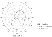
请参阅图21a至图21d,图21a至图21c是本申请提供的电子设备1000中天线系统800在2.4GHz分别在XY平面、XZ平面和ZY平面内的远场方向图。从各个结果图可以看出,天线系统800在2.4GHz在XY平面、ZY平面具有较好的信号覆盖广度。图21d是本申请提供的电子设备1000中天线系统800在2.4GHz的方向图,从方向图可以看出天线系统800在2.4GHz在XZ平面具有较高的增益。Please refer to FIGS. 21 a to 21 d . FIGS. 21 a to 21 c are far-field patterns of the antenna system 800 in the XY plane, the XZ plane and the ZY plane respectively at 2.4 GHz in the electronic device 1000 provided by the present application. It can be seen from each result graph that the antenna system 800 has good signal coverage in the XY plane and the ZY plane at 2.4 GHz. 21d is a directional diagram of the antenna system 800 at 2.4 GHz in the electronic device 1000 provided by the present application. It can be seen from the directional diagram that the antenna system 800 has a higher gain in the XZ plane at 2.4 GHz.
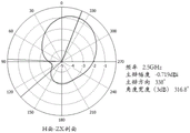
请参阅图22a至图22d,图22a至图22c是本申请提供的电子设备1000中天线系统800在2.45GHz分别在XY平面、XZ平面和ZY平面内的远场方向图。从各个结果图可以看出,天线系统800在2.45GHz在XY平面、ZY平面具有较好的信号覆盖广度。图22d是本申请提供的电子设备1000中天线系统800在2.45GHz的方向图,从方向图可以看出天线系统800在2.45GHz在XZ平面具有较高的增益。Please refer to FIGS. 22 a to 22 d . FIGS. 22 a to 22 c are far-field patterns of the antenna system 800 in the XY plane, the XZ plane and the ZY plane respectively at 2.45 GHz in the electronic device 1000 provided by the present application. It can be seen from each result graph that the antenna system 800 has good signal coverage in the XY plane and the ZY plane at 2.45 GHz. FIG. 22d is a directional diagram of the antenna system 800 at 2.45 GHz in the electronic device 1000 provided by the present application. It can be seen from the directional diagram that the antenna system 800 has a higher gain in the XZ plane at 2.45 GHz.
请参阅图23a至图23d,图23a至图23c是本申请提供的电子设备1000中天线系统800在2.5GHz分别在XY平面、XZ平面和ZY平面内的远场方向图。从各个结果图可以看出,天线系统800在2.5GHz在XY平面、ZY平面具有较好的信号覆盖广度。图23d是本申请提供的电子设备1000中天线系统800在2.5GHz的方向图,从方向图可以看出天线系统800在2.5GHz在XZ平面具有较高的增益。Please refer to FIGS. 23 a to 23 d . FIGS. 23 a to 23 c are far-field patterns of the antenna system 800 in the XY plane, the XZ plane and the ZY plane respectively at 2.5 GHz in the electronic device 1000 provided by the present application. It can be seen from each result graph that the antenna system 800 has good signal coverage in the XY plane and the ZY plane at 2.5 GHz. 23d is a directional diagram of the antenna system 800 at 2.5 GHz in the electronic device 1000 provided by the present application. It can be seen from the directional diagram that the antenna system 800 has a higher gain in the XZ plane at 2.5 GHz.
请参阅图24,图24是本申请提供的电子设备1000中天线系统800的效率图。从效率图可以看出,天线系统800在2.4GHz~2.5GHz的效率在-4dB左右,相较于常规的可穿戴内置天线在Wi-Fi 2.4G频段的天线效率性能平均在-5dB左右,故本申请的天线效率大于或等于-4dB,这反映了相较于常规更好的天线性能。Please refer to FIG. 24 , which is an efficiency diagram of the antenna system 800 in the electronic device 1000 provided by the present application. It can be seen from the efficiency diagram that the efficiency of the antenna system 800 at 2.4GHz to 2.5GHz is about -4dB. Compared with the conventional wearable built-in antenna, the antenna efficiency performance in the Wi-Fi 2.4G frequency band is about -5dB on average. The antenna efficiency of the present application is greater than or equal to -4dB, which reflects better antenna performance compared to conventional.
在相同外观尺寸限制条件下,采用本申请提供的小型共形天线方案,不占用主板210周边空间,复用电子设备1000中电池组件500与壳体组件100之间的本身空间,不会改变设备本身的外观尺寸,可以节省空间,帮助主板210布局更丰富的功能电路,主板210的布局可以做到优化;复用与电池组件500中的金属体530作为参考地,实现了元件的复用,节省主板210周侧的空间的同时能实现较优的天线性能。Under the same appearance and size constraints, the small conformal antenna solution provided by the present application does not occupy the surrounding space of the main board 210, reuses the space between the battery assembly 500 and the housing assembly 100 in the electronic device 1000, and does not change the device. The appearance size of itself can save space, help the main board 210 to layout more abundant functional circuits, and the layout of the main board 210 can be optimized; reuse and the metal body 530 in the battery assembly 500 as a reference ground, realize the reuse of components, While saving the space around the main board 210, better antenna performance can be achieved.
以上所述是本申请的部分实施方式,应当指出,对于本技术领域的普通技术人员来说,在不脱离本申请原理的前提下,还可以做出若干改进和润饰,这些改进和润饰也视为本申请的保护范围。The above are some embodiments of the present application. It should be pointed out that for those skilled in the art, without departing from the principles of the present application, several improvements and modifications can also be made, and these improvements and modifications may also be regarded as The protection scope of this application.