CN203455796U - Touch structure - Google Patents
Touch structure Download PDFInfo
- Publication number
- CN203455796U CN203455796U CN201320506757.9U CN201320506757U CN203455796U CN 203455796 U CN203455796 U CN 203455796U CN 201320506757 U CN201320506757 U CN 201320506757U CN 203455796 U CN203455796 U CN 203455796U
- Authority
- CN
- China
- Prior art keywords
- refraction layer
- touch
- layer
- low
- optical
- Prior art date
- Legal status (The legal status is an assumption and is not a legal conclusion. Google has not performed a legal analysis and makes no representation as to the accuracy of the status listed.)
- Expired - Fee Related
Links
- 230000003287 optical effect Effects 0.000 claims abstract description 40
- 239000000463 material Substances 0.000 claims description 12
- 229910004298 SiO 2 Inorganic materials 0.000 claims description 3
- 229910010413 TiO 2 Inorganic materials 0.000 claims description 3
- 230000002093 peripheral effect Effects 0.000 abstract description 6
- 239000010410 layer Substances 0.000 description 80
- 238000005530 etching Methods 0.000 description 11
- 238000010586 diagram Methods 0.000 description 10
- 238000002834 transmittance Methods 0.000 description 8
- 238000000034 method Methods 0.000 description 7
- 239000000758 substrate Substances 0.000 description 7
- 239000012790 adhesive layer Substances 0.000 description 4
- 239000004020 conductor Substances 0.000 description 4
- 239000003292 glue Substances 0.000 description 4
- 239000004973 liquid crystal related substance Substances 0.000 description 3
- 238000000059 patterning Methods 0.000 description 3
- 230000035515 penetration Effects 0.000 description 3
- 239000004372 Polyvinyl alcohol Substances 0.000 description 2
- 229910052751 metal Inorganic materials 0.000 description 2
- 239000002184 metal Substances 0.000 description 2
- 239000012994 photoredox catalyst Substances 0.000 description 2
- 229920002120 photoresistant polymer Polymers 0.000 description 2
- 229920003229 poly(methyl methacrylate) Polymers 0.000 description 2
- 239000004417 polycarbonate Substances 0.000 description 2
- 239000004926 polymethyl methacrylate Substances 0.000 description 2
- 229920002451 polyvinyl alcohol Polymers 0.000 description 2
- XLYOFNOQVPJJNP-UHFFFAOYSA-N water Substances O XLYOFNOQVPJJNP-UHFFFAOYSA-N 0.000 description 2
- 238000001039 wet etching Methods 0.000 description 2
- 229920002284 Cellulose triacetate Polymers 0.000 description 1
- 241000699666 Mus <mouse, genus> Species 0.000 description 1
- 241000699670 Mus sp. Species 0.000 description 1
- 239000004820 Pressure-sensitive adhesive Substances 0.000 description 1
- NNLVGZFZQQXQNW-ADJNRHBOSA-N [(2r,3r,4s,5r,6s)-4,5-diacetyloxy-3-[(2s,3r,4s,5r,6r)-3,4,5-triacetyloxy-6-(acetyloxymethyl)oxan-2-yl]oxy-6-[(2r,3r,4s,5r,6s)-4,5,6-triacetyloxy-2-(acetyloxymethyl)oxan-3-yl]oxyoxan-2-yl]methyl acetate Chemical compound O([C@@H]1O[C@@H]([C@H]([C@H](OC(C)=O)[C@H]1OC(C)=O)O[C@H]1[C@@H]([C@@H](OC(C)=O)[C@H](OC(C)=O)[C@@H](COC(C)=O)O1)OC(C)=O)COC(=O)C)[C@@H]1[C@@H](COC(C)=O)O[C@@H](OC(C)=O)[C@H](OC(C)=O)[C@H]1OC(C)=O NNLVGZFZQQXQNW-ADJNRHBOSA-N 0.000 description 1
- 239000000853 adhesive Substances 0.000 description 1
- 230000001070 adhesive effect Effects 0.000 description 1
- 230000009286 beneficial effect Effects 0.000 description 1
- 238000000576 coating method Methods 0.000 description 1
- 238000004891 communication Methods 0.000 description 1
- 239000002131 composite material Substances 0.000 description 1
- 238000001312 dry etching Methods 0.000 description 1
- 238000001035 drying Methods 0.000 description 1
- 230000000694 effects Effects 0.000 description 1
- 239000011521 glass Substances 0.000 description 1
- AMGQUBHHOARCQH-UHFFFAOYSA-N indium;oxotin Chemical compound [In].[Sn]=O AMGQUBHHOARCQH-UHFFFAOYSA-N 0.000 description 1
- 230000010354 integration Effects 0.000 description 1
- 238000004519 manufacturing process Methods 0.000 description 1
- 238000005259 measurement Methods 0.000 description 1
- 230000001681 protective effect Effects 0.000 description 1
- 239000011241 protective layer Substances 0.000 description 1
- 239000006058 strengthened glass Substances 0.000 description 1
- 230000000007 visual effect Effects 0.000 description 1
Images


Landscapes
- Position Input By Displaying (AREA)
Abstract
本实用新型的触控结构包含:显示单元、偏光板以及触控感测结构,偏光板设置于显示单元之上,具有至少一光学折射层,以及触控感测结构设置于光学折射层的一侧(可设置于其之下或其之上),触控感测结构更具有复数感测串列和复数周边线路分别电性连接。

The touch control structure of the utility model comprises: a display unit, a polarizing plate and a touch control sensing structure. The polarizing plate is arranged on the display unit and has at least one optical refractive layer. The touch control sensing structure is arranged on one side of the optical refractive layer (it can be arranged below or above the optical refractive layer). The touch control sensing structure further has a plurality of sensing series and a plurality of peripheral circuits which are electrically connected respectively.
Description
技术领域 technical field
本实用新型有关一种触控结构,尤指一种将复数光学折射层应用于触控结构,以提升穿透率。 The utility model relates to a touch control structure, in particular to a touch control structure in which multiple optical refraction layers are applied to improve the penetration rate.
背景技术 Background technique
在现今各式消费性电子产品的市场中,个人数字助理(PDA)、行动电话(mobile Phone)、笔记型电脑(notebook)及平板电脑(tablet PC)等可携式电子产品皆已广泛的使用触控式面板(touch panel)作为其资料沟通的界面工具。此外,由于目前电子产品的设计皆以轻、薄、短、小为方向,因此在产品上无足够空间容纳如键盘、鼠标等传统输入装置,尤其在讲求人性化设计的平板电脑需求的带动下,触控式面板已经一跃成为关键的零组件之一。而且触控式面板除了符合可作多层次选单设计要求外,亦能同时拥有键盘、鼠标等的功能及手写输入等人性化的操作方式,尤其将输入与输出整合在同一介面(荧幕)的特质,更是其它传统输入装置所不及之处。 In today's market of various consumer electronics products, portable electronic products such as personal digital assistants (PDAs), mobile phones (mobile phones), notebook computers (notebooks) and tablet computers (tablet PCs) have been widely used The touch panel is used as an interface tool for data communication. In addition, since the current design of electronic products is light, thin, short, and small, there is not enough space on the product to accommodate traditional input devices such as keyboards and mice, especially driven by the demand for tablet computers that emphasize humanized design. , The touch panel has become one of the key components. Moreover, the touch panel can not only meet the requirements of multi-level menu design, but also have the functions of keyboard, mouse and other humanized operation methods such as handwriting input, especially the integration of input and output on the same interface (screen). Features, which are beyond the reach of other traditional input devices.
目前触控面板制造过程中,图案化制程可分为干式制程与湿式制程。触控面板上的透明导电层主要是由铟锡氧化物(indium tin oxide, ITO)所组成,由于导电层的镀膜方式基本上为整个平面,因此,若要在已溅镀完成的基板上形成图案,需将导电层进行蚀刻。目前蚀刻的方式有两种,分别为湿式蚀刻与干式蚀刻,其中湿式蚀刻的图案化是由光罩所形成,采用两道蚀刻制程,其为金属层蚀刻以及导电层蚀刻。在制作透明感应电极图案化过程中,利用上光阻→曝光→显影→蚀刻→去光阻…等步骤,将透明导电层图案化形成透明感应电极于透明基材的表面。然而因为透明基材与透明导电层两者材料的光学折射率不同,容易产生视觉可见的透明导电图形痕迹或蚀刻痕迹而影响触控面板的外观,目前此一课题尚未有良好的解决之道。 In the current touch panel manufacturing process, the patterning process can be divided into a dry process and a wet process. The transparent conductive layer on the touch panel is mainly composed of indium tin oxide (ITO). Since the coating method of the conductive layer is basically the entire plane, if it is to be formed on a substrate that has been sputtered pattern, the conductive layer needs to be etched. There are currently two etching methods, namely wet etching and dry etching. The patterning of wet etching is formed by a photomask, and two etching processes are used, which are metal layer etching and conductive layer etching. In the patterning process of making the transparent sensing electrode, the transparent conductive layer is patterned to form the transparent sensing electrode on the surface of the transparent substrate by using steps such as applying photoresist→exposure→developing→etching→removing the photoresist. However, due to the difference in optical refractive index between the transparent substrate and the transparent conductive layer, it is easy to produce visible traces of transparent conductive patterns or etching traces and affect the appearance of the touch panel. At present, there is no good solution to this problem.
实用新型内容 Utility model content
本实用新型所解决的技术问题即在提供一种可据以改善或降低电极图形痕迹或蚀刻痕迹的触控结构。 The technical problem solved by the utility model is to provide a touch structure that can improve or reduce the traces of electrode patterns or etching traces.
本实用新型所采用的技术手段如下所述。 The technical means adopted in the utility model are as follows.
为达上揭目的,本实用新型的触控结构包含:显示单元、偏光板以及触控感测结构,偏光板设置于显示单元之上,具有至少一光学折射层,以及触控感测结构设置于光学折射层之下,触控感测结构更具有复数感测串列和复数周边线路分别电性连接。 To achieve the above disclosure, the touch structure of the present invention includes: a display unit, a polarizer and a touch sensing structure, the polarizer is arranged on the display unit, has at least one optical refraction layer, and the touch sensing structure is set Under the optical refraction layer, the touch sensing structure further has a plurality of sensing series and a plurality of peripheral circuits electrically connected respectively.
为达上述目的,所述触控结构,其中光学折射层更包括:至少一高折射层和至少一低折射层,高折射层设置于偏光板的一下表面,低折射层设置于高折射层之下。 To achieve the above purpose, the touch structure, wherein the optical refraction layer further includes: at least one high refraction layer and at least one low refraction layer, the high refraction layer is arranged on the lower surface of the polarizing plate, and the low refraction layer is arranged on the high refraction layer Down.
为达上述目的,所述触控结构,其中光学折射层更包括至少一高折射层和至少一低折射层,触控感测结构位于偏光板的一上表面,低折射层设置于触控感测结构之上,高折射层设置于低折射层之上。 To achieve the above purpose, the touch structure, wherein the optical refraction layer further includes at least one high refraction layer and at least one low refraction layer, the touch sensing structure is located on an upper surface of the polarizer, and the low refraction layer is arranged on the touch sensor On the measurement structure, the high refraction layer is disposed on the low refraction layer.
本实用新型并提供另种触控结构,其包含:显示单元、偏光板以及触控感测结构,偏光板设置于显示单元之上,具有至少一光学折射层,以及触控感测结构设置于光学折射层之上,触控感测结构更具有复数感测串列和复数周边线路分别电性连接。 The utility model also provides another touch structure, which includes: a display unit, a polarizing plate and a touch sensing structure, the polarizing plate is disposed on the display unit, has at least one optical refraction layer, and the touch sensing structure is disposed on On the optical refraction layer, the touch sensing structure further has a plurality of sensing series and a plurality of peripheral circuits electrically connected respectively.
为达上述目的,所述触控结构,其中光学折射层更包括至少一高折射层和至少一低折射层,每一高折射层和每一低折射层相互交错堆栈。 To achieve the above purpose, the touch structure, wherein the optical refraction layer further includes at least one high refraction layer and at least one low refraction layer, each high refraction layer and each low refraction layer are stacked alternately.
上述高折射层的折射率为1.6至2.4,低折射层的折射率为1.2至1.6。 The refractive index of the above-mentioned high refractive layer is 1.6 to 2.4, and the refractive index of the low refractive layer is 1.2 to 1.6.
为达上述目的,所述触控结构,其中高折射层材质可为ITO、TiO2或Nb2O5,低折射层材质可为MgF2、SiO2或MgO。 To achieve the above purpose, in the touch structure, the material of the high refraction layer can be ITO, TiO 2 or Nb 2 O 5 , and the material of the low refraction layer can be MgF 2 , SiO 2 or MgO.
本实用新型所产生的有益效果为:改善或降低电极图形痕迹或蚀刻痕迹。 The beneficial effects produced by the utility model are: improving or reducing traces of electrode patterns or etching traces.
附图说明 Description of drawings
图1所示为本实用新型中触控结构的第一实施例示意图。 FIG. 1 is a schematic diagram of the first embodiment of the touch structure in the present invention.
图2所示为本实用新型中触控结构的第二实施例示意图。 FIG. 2 is a schematic diagram of a second embodiment of the touch structure in the present invention.
图3所示为本实用新型中触控结构的第三实施例示意图。 FIG. 3 is a schematic diagram of a third embodiment of the touch structure in the present invention.
图4所示为本实用新型中触控结构的第四实施例示意图。 FIG. 4 is a schematic diagram of a fourth embodiment of the touch structure in the present invention.
图5所示为本实用新型中触控结构的第五实施例示意图。 FIG. 5 is a schematic diagram of a fifth embodiment of the touch structure in the present invention.
图号说明: Description of figure number:
偏光板110,210,310,410,510,610,710 Polarizer 110,210,310,410,510,610,710
复数光学折射层140
Plural
高折射层220,320,420,520,620,720
低折射层230,330,430,530,630,730 Low refractive layer230,330,430,530,630,730
触控感测结构111,211,311,411,511,611,711 Touch sensing structure111,211,311,411,511,611,711
显示单元112,212,312,412,512 Display unit 112,212,312,412,512
透明导电层613,713 Transparent conductive layer613,713
金属层614,714 Metal layers614,714
复数感测串列118,218,318,418,518,618,718 Complex sensing series 118,218,318,418,518,618,718
复数周边线路118,219,319,419,519,619,719 Multiple surrounding lines 118,219,319,419,519,619,719
黏着层115,215 Adhesive layer115,215
硬质透明基板216。
Hard
具体实施方式 Detailed ways
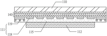
请参阅图1所示为本实用新型第一实施例的触控结构示意图。首先,本实用新型的触控结构包括显示单元112、偏光板110以及触控感测结构111;其中显示单元112例如可为液晶显示器(liquid crystal display,LCD)、有机发光二极管显示器(organic light emitting diode display,OLED display)、电泳显示器(electrophoretic display,EPD)、等离子显示器(Plasma Display Panel)或电子纸显示器(E-paper Display)等,然并不以此为限。
Please refer to FIG. 1 which is a schematic diagram of the touch structure of the first embodiment of the present invention. First, the touch control structure of the present invention includes a
偏光板110设置于显示单元112之上,藉由偏光板110极化偏光可控制显示效果,其中偏光板110的主要结构例如可为PET保护膜、PSA感压性黏着剂、TAC三醋酸纤维素、PVA聚乙烯醇与PET离型膜等,然并不以此为限。偏光板110并具有至少一光学折射层140。
The polarizing
触控感测结构111设置于至少一光学层140之下,其中触控感测结构可以为电容式触控结构,然并不以此为限。于本实施例中触控感测结构更具有复数感测串列118和复数周边线路119,复数感测串列118分别与复数周边线119路电性连接(图未示)。复数感测串列118由复数感测垫和复数桥接线串接所构成(图未示)。
The
偏光板110与显示单元112之间更包括黏着层115,黏着偏光板110与显示单元112。其中黏着层115的材质可为光学胶或水胶。其中,藉由至少一光学折射层140产生不同的光学特性,可使触控感测结构的复数感测串列118和复数周边线路119所形成的图形痕迹或蚀刻痕迹淡化,进而增加整体触控结构的穿透率。
An
请参阅图2所示为本实用新型第二实施例的触控结构示意图。其触控结构同样包括有显示单元212、偏光板210以及触控感测结构211;其中,光学折射层更包括至少一高折射层220和至少一低折射层230相互交错堆栈,于本实施例中具有一高折射层220,其折射率为1.6至2.4,材质例如可为ITO、TiO2或Nb2O5等物质,但并不设限于此,以及具有一低折射层230,其折射率为1.2至1.6,材质例如可为MgF2、SiO2或MgO等物质,但并不设限于此;其中,高折射层220设置于偏光板210的一下表面,低折射层230设置于高折射层220之下。触控感测结构211位于低折射层230之下,由于触控感测结构211具有复数感测串列218由透明导电材料所形成,其折射率为1.8~2.4,折射率较高,再搭配高折射层220和低折射层230的排列,形成高折射率/低折射率/高折射率的搭配,可使穿透度提升,并且使短波长穿透度提升,将有效改善触控面板的光学性质与外观。
Please refer to FIG. 2 which is a schematic diagram of the touch structure of the second embodiment of the present invention. Its touch control structure also includes a
并有一硬质透明基板216设置于偏光板210之上,硬质透明基板216的材质例如可为玻璃、强化玻璃、PC、PMMA或PC与PMMA的复合材,作为液晶面板外层的保护层(cover lens),其中,硬质透明基板216与偏光板210之间更包括以黏着层215相互黏贴,黏着层215的材质可为光学胶或水胶。
And a hard
请参阅图3所示为本实用新型第三实施例的触控结构示意图。其触控结构同样包括有显示单元312、偏光板310以及触控感测结构311;其中,光学折射层更包括至少一高折射层320和至少一低折射层330,而触控感测结构311位于偏光板310的一上表面,低折射层330设置于触控感测结构311之上,高折射层320设置于低折射层330之上。高折射层320与低折射层330的搭配不以此为限。由于触控感测结构211具有复数感测串列318由透明导电材料所形成,其折射率为1.8~2.4,折射率较高,再搭配高折射层320和低折射层330的排列,形成高折射率/低折射率/高折射率的搭配,可使穿透度提升,并且使短波长穿透度提升,将有效改善触控面板的光学性质与外观。
Please refer to FIG. 3 which is a schematic diagram of the touch structure of the third embodiment of the present invention. Its touch control structure also includes a display unit 312, a polarizer 310, and a touch sensing structure 311; wherein, the optical refraction layer further includes at least one high refraction layer 320 and at least one low refraction layer 330, and the touch sensing structure 311 Located on an upper surface of the polarizer 310 , the low refraction layer 330 is disposed on the touch sensing structure 311 , and the high refraction layer 320 is disposed on the low refraction layer 330 . The combination of the high refraction layer 320 and the low refraction layer 330 is not limited thereto. Since the
请参阅图4所示为本实用新型的第四实施例的触控结构示意图。本实用新型的触控结构同样包括显示单元412、偏光板410以及触控感测结构411;其中,触控感测结构411设置于光学折射层440之上;如图所示的实施例中,光学折射层包括至少一高折射层420和至少一低折射层430,高折射层420设置于偏光板410的一上表面,低折射层430设置于高折射层420之上。由于触控感测结构211具有复数感测串列318由透明导电材料所形成,其折射率为1.8~2.4,折射率较高,再搭配高折射层320和低折射层330的排列,形成高折射率/低折射率/高折射率的搭配,可使穿透度提升,并且使短波长穿透度提升,将有效改善触控面板的光学性质与外观。
Please refer to FIG. 4 , which is a schematic diagram of the touch structure of the fourth embodiment of the present invention. The touch control structure of the present invention also includes a
请参阅图5所示为本实用新型的第五实施例的触控结构示意图。本实用新型的触控结构同样包括显示单元512、偏光板510以及触控感测结构511;其中,光学折射层包括至少一高折射层520和至少一低折射层530,触控感测结构511位于偏光板510的一下表面,低折射层530设置于触控感测结构511之下,高折射层520设置于低折射层530之下。由于触控感测结构211具有复数感测串列318由透明导电材料所形成,其折射率为1.8~2.4,折射率较高,再搭配高折射层320和低折射层330的排列,形成高折射率/低折射率/高折射率的搭配,可使穿透度提升,并且使短波长穿透度提升,将有效改善触控面板的光学性质与外观。
Please refer to FIG. 5 which is a schematic diagram of the touch structure of the fifth embodiment of the present invention. The touch structure of the present utility model also includes a display unit 512, a polarizer 510, and a touch sensing structure 511; wherein, the optical refraction layer includes at least one high refraction layer 520 and at least one low refraction layer 530, and the touch sensing structure 511 Located on the lower surface of the polarizing plate 510 , the low refraction layer 530 is disposed under the touch sensing structure 511 , and the high refraction layer 520 is disposed under the low refraction layer 530 . Since the
本实用新型提供一种可据以改善或降低电极图形痕迹或蚀刻痕迹的技术手段。在偏光板表面先形成复数迭层组合的光学折射层,利用光学折射层的材料和厚度而产生不同的光学特性,使偏光板表面的透明导电图形痕迹或蚀刻痕迹淡化,进而增加整体触控结构的穿透率,并可提升整体触控面板的视觉外观。 The utility model provides a technical means which can improve or reduce electrode pattern traces or etching traces. On the surface of the polarizer, an optical refraction layer composed of multiple laminated layers is first formed, and the material and thickness of the optical refraction layer are used to produce different optical characteristics, so that the traces of transparent conductive patterns or etching marks on the surface of the polarizer are diluted, thereby increasing the overall touch structure. Penetration rate, and can improve the visual appearance of the overall touch panel.
Claims (9)
Priority Applications (1)
| Application Number | Priority Date | Filing Date | Title |
|---|---|---|---|
| CN201320506757.9U CN203455796U (en) | 2013-08-19 | 2013-08-19 | Touch structure |
Applications Claiming Priority (1)
| Application Number | Priority Date | Filing Date | Title |
|---|---|---|---|
| CN201320506757.9U CN203455796U (en) | 2013-08-19 | 2013-08-19 | Touch structure |
Publications (1)
| Publication Number | Publication Date |
|---|---|
| CN203455796U true CN203455796U (en) | 2014-02-26 |
Family
ID=50135657
Family Applications (1)
| Application Number | Title | Priority Date | Filing Date |
|---|---|---|---|
| CN201320506757.9U Expired - Fee Related CN203455796U (en) | 2013-08-19 | 2013-08-19 | Touch structure |
Country Status (1)
| Country | Link |
|---|---|
| CN (1) | CN203455796U (en) |
Cited By (3)
| Publication number | Priority date | Publication date | Assignee | Title |
|---|---|---|---|---|
| CN104423654A (en) * | 2013-08-19 | 2015-03-18 | 杰圣科技股份有限公司 | Touch control structure and manufacturing method thereof |
| CN105278710A (en) * | 2014-06-17 | 2016-01-27 | 恒颢科技股份有限公司 | Touch control display |
| CN105572937A (en) * | 2015-12-23 | 2016-05-11 | 联想(北京)有限公司 | Touch assembly and electronic equipment |
-
2013
- 2013-08-19 CN CN201320506757.9U patent/CN203455796U/en not_active Expired - Fee Related
Cited By (4)
| Publication number | Priority date | Publication date | Assignee | Title |
|---|---|---|---|---|
| CN104423654A (en) * | 2013-08-19 | 2015-03-18 | 杰圣科技股份有限公司 | Touch control structure and manufacturing method thereof |
| CN105278710A (en) * | 2014-06-17 | 2016-01-27 | 恒颢科技股份有限公司 | Touch control display |
| CN105278710B (en) * | 2014-06-17 | 2018-06-29 | 恒颢科技股份有限公司 | Touch control display |
| CN105572937A (en) * | 2015-12-23 | 2016-05-11 | 联想(北京)有限公司 | Touch assembly and electronic equipment |
Similar Documents
| Publication | Publication Date | Title |
|---|---|---|
| TWI525499B (en) | Touch display panel | |
| CN104765505B (en) | A kind of touch-control display panel, manufacturing method and display device | |
| US11360618B2 (en) | Method for manufacturing touch screen, display device | |
| TW201541324A (en) | Touch display panel | |
| CN207380686U (en) | Touch panel and apply its display device | |
| CN105702701A (en) | Piezoelectric touch organic light-emitting display panel and manufacturing method thereof, and organic light-emitting display | |
| TWI566155B (en) | Capacitive touch panel | |
| KR20140035276A (en) | Touch panel and manufacturing method thereof | |
| CN203982335U (en) | Touch control display apparatus | |
| CN203455796U (en) | Touch structure | |
| CN201218887Y (en) | Capacitive touch display panel | |
| CN203909741U (en) | Touch control display panel | |
| CN204009808U (en) | Touch control display apparatus | |
| CN203909742U (en) | Touch control display panel | |
| US20150136450A1 (en) | Touch panel and method of manufacturing the same | |
| TW201411231A (en) | Touch panel and manufacturing method | |
| CN203930729U (en) | Touch-control display panel | |
| TW201403176A (en) | Touch panel and manufacturing method | |
| TWI634470B (en) | Polarized capacitive touch panel and display of the same | |
| CN103914164A (en) | touch panel | |
| CN202394196U (en) | Touch control sensing device and electronic device | |
| TW201310290A (en) | Touch panel and method for fabricating the same, and display device comprising the same | |
| CN104281302A (en) | Touch structure and manufacturing method thereof | |
| CN203849705U (en) | Touch display structure | |
| TWI485596B (en) | Touch panel and manufacturing method |
Legal Events
| Date | Code | Title | Description |
|---|---|---|---|
| C14 | Grant of patent or utility model | ||
| GR01 | Patent grant | ||
| CF01 | Termination of patent right due to non-payment of annual fee | ||
| CF01 | Termination of patent right due to non-payment of annual fee |
Granted publication date: 20140226 Termination date: 20160819 |