The light-emitting diode assembly that is used for backlight module
Technical field
The utility model relates to a kind of light-emitting diode assembly, relates in particular to a kind of light-emitting diode assembly that is used for backlight module.
Background technology
Because light-emitting diode has characteristics such as energy-saving and environmental protection, is used for the backlight liquid crystal display module and also gradually adopts light-emitting diode as light source.Distinguish with respect to the position of light guide plate according to light source, backlight module can roughly be divided into two kinds of side entering type and straight-down negatives.
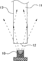
As shown in Figure 1, existing side entrance back module be with light-emitting diode 10 as light source, be arranged at 12 places, a wherein side of light guide plate 11 upper sides or lower side.Light-emitting diode 10 launches light in the light guide plate 11 via this side 12, and transmits in light guide plate 11.And under the trend of LCD slimming, its associated component also needs thinning thereupon.
Yet, the continuous thinning of light guide plate 11 but can cause its light inlet difficulty, as shown in Figure 2, because the light that light-emitting diode 10 itself is sent has an angle of divergence, after this light is injected this light guide plate 11 via the side 12 of light guide plate 11, the light of part wide-angle can outwards reflect from exiting surface 13, causes light guide plate 11 contiguous these light-emitting diode 10 places to form local bright, the uneven phenomenon of bright dipping that causes backlight module to produce.
The utility model content
A purpose of the present utility model is to provide a kind of light-emitting diode with asymmetric divergence of beam angle, can axially provide less divergence of beam angle in one, to solve the above-mentioned uneven phenomenon of backlight module bright dipping that causes.
For achieving the above object, the utility model provides a kind of light-emitting diode assembly that is used for backlight module, comprises:
One substrate;
A plurality of submounts are arranged on this substrate;
A plurality of luminescence chips are arranged at respectively on these a plurality of submounts; And
A plurality of package lens are arranged at respectively on these a plurality of luminescence chips, and respectively this package lens is a solid semielliptical shape, and have the lens minor axis of a lens major axis and vertical this lens major axis.
The above-mentioned light-emitting diode assembly that is used for backlight module, wherein, this substrate is a long strip type and has a substrate major axis, and parallel this substrate major axis of this lens major axis.
The above-mentioned light-emitting diode assembly that is used for backlight module, wherein, this luminescence chip is a cuboid, and the major axis of this cuboid is parallel to the lens major axis of this package lens.
The above-mentioned light-emitting diode assembly that is used for backlight module, wherein, this package lens is a silica gel material part.
The above-mentioned light-emitting diode assembly that is used for backlight module, wherein, the silica gel material part of this package lens for penetrating for the visible light of 400~780nm wave band.
The above-mentioned light-emitting diode assembly that is used for backlight module, wherein, the height of this package lens is at least 0.5mm.
The above-mentioned light-emitting diode assembly that is used for backlight module, wherein, the length of this lens major axis is greater than the length of this lens minor axis.
The above-mentioned light-emitting diode assembly that is used for backlight module wherein, also is provided with the fluorescent material of dispersion in this package lens.
Effect of the present utility model is, on this luminescence chip, so that asymmetric divergence of beam angle to be provided, solves the uneven phenomenon of above-mentioned bright dipping by the package lens that this semielliptical shape is provided.
Below in conjunction with the drawings and specific embodiments the utility model is described in detail, but not as to qualification of the present utility model.
Description of drawings
Fig. 1 is an existing use schematic diagram that is used for the light-emitting diode assembly of backlight module;
Fig. 2 is existing another use schematic diagram that is used for the light-emitting diode assembly of backlight module;
Fig. 3 is used for a schematic diagram of the light-emitting diode assembly of backlight module for the utility model;
Fig. 4 is used for a schematic top plan view of the light-emitting diode assembly of backlight module for the utility model;
Fig. 5 is used for a schematic side view of the light-emitting diode assembly of backlight module for the utility model;
Fig. 6 is used for another schematic side view of the light-emitting diode assembly of backlight module for the utility model.
Wherein, Reference numeral
Substrate 21 luminescence chips 22
Package lens 23 substrate major axis I
Lens major axis X lens minor axis Y
Height h section upper limb 231,232
Submounts 24 light guide plate 30
Side 31
Embodiment
Relevant technology contents of the present utility model and detailed description now cooperate graphic being described as follows:
As shown in Figure 3, a preferred embodiment that is used for the light-emitting diode assembly of backlight module of the present utility model, this light-emitting diode assembly that is used for backlight module mainly comprises a substrate 21, a plurality of submounts 24, a plurality of luminescence chip 22, and quantity is to package lens 23 that should a plurality of luminescence chips 22.It should be noted that, in the present embodiment, the quantity of luminescence chip 22 be with 11 be example explanation, yet during actual enforcement, the quantity of luminescence chip 22 gets final product at least one.
This substrate 21 is various rigid or soft printed circuit board (PCB)s, also can be the good aluminium base of radiating efficiency, has many circuit on it, and a plurality of contact (figure does not show) that supplies luminescence chip 22 to be electrically connected with circuit.In the present embodiment, this substrate 21 is a long strip type and has a substrate major axis I, does not limit with this during actual enforcement.
These a plurality of submounts 24 are arranged on this substrate 21, and this submounts 24 can be various rigid or soft printed circuit board (PCB)s, and it act as this luminescence chip 22 of carrying and package lens 23.These a plurality of submounts 24 have can be for the circuit of luminescence chip 23 electrical connections.These a plurality of submounts 24 can routing joint (wirebonding) or surface mount modes such as (surface mounting) be electrically connected with this substrate 21.
By these a plurality of submounts 24 one side carryings these a plurality of luminescence chips 22 and these a plurality of package lens 23, another side is electrically connected with this substrate 21, can be arbitrary therein luminescence chip 22 when losing efficacy, directly remove in the lump, and replace and go up identical assembly with it and with the submounts 24 of its below.Because with the process that submounts 24 removes on this substrate 21, it is easy to be many to compare the existing process that luminescence chip need be removed on substrate, so the practice can be improved the inconvenience that needed dismounting luminescence chip 22 when luminescence chip 22 lost efficacy.
These a plurality of luminescence chips 22 compartment of terrains are arranged on this submounts 24, and are electrically connected with this submounts 24.The mode visible die kind that is electrically connected adopts routing to engage (wire bonding) or chip bonding (flip-chip bonding).These a plurality of luminescence chips 22 are the light-emitting diode chip for backlight unit of semiconductor material, and its issued light look does not limit.Preferably, this luminescence chip 22 can be the cuboid shown in the figure, obtains bigger light-emitting area by the shape of cuboid, to obtain preferable luminous efficiency.
As shown in Figure 4, these a plurality of package lens 23 are arranged at respectively on these a plurality of luminescence chips 22 contiguously, coat these a plurality of luminescence chips 22 respectively.These a plurality of package lens 23 respectively are a solid semielliptical shape, and have the lens minor axis Y of a lens major axis X and vertical this lens major axis X.And, this substrate major axis of this lens major axis X almost parallel I, and the major axis of this luminescence chip 22 is roughly parallel to the lens major axis X of this package lens 23.This package lens 23 is made with transparent materials such as silica gel, and only this silica gel is required to be and can penetrates for the visible light of 400~780nm wave band.When practical application, the height h of this package lens 23 need be at least 0.5mm, and the length of this lens major axis X is greater than the length of this lens minor axis Y.In addition, this package lens 23 also can add fluorescent material, this package lens 23 is had be scattered in the fluorescent material in it, in order to 22 isolychns of this luminescence chip of absorption portion, and is converted into the light of another wavelength, reaches the effect of mixed light whereby.
As Fig. 5 and shown in Figure 6, because the length of this lens major axis X is greater than the length of this lens minor axis Y, therefore, this package lens 23 of Fig. 5 is along the curvature of the section upper limb 231 of its lens minor axis Y, is little than this package lens 23 of Fig. 6 along the curvature of the section upper limb 232 of its lens minor axis X.Because the light that the section upper limb 231 than small curve can make luminescence chip 22 be sent that has of Fig. 5 has the less angle of divergence, therefore, after light is injected this light guide plate 30 via the side 31 of light guide plate 30, be difficult for refraction outside light guide plate 30 and form local bright, can prevent effectively that the phenomenon of the bright dipping inequality of backlight module from taking place.
On the other hand, as shown in Figure 6, because the light that the section upper limb 232 than deep camber can make luminescence chip 22 be sent that has of Fig. 6 has the bigger angle of divergence, therefore, after light is injected this light guide plate 30 via the side 31 of light guide plate 30, but wide-angle ground spreads in light guide plate 30, also can effectively improve the uniformity of luminance of backlight module.
Certainly; the utility model also can have other various embodiments; under the situation that does not deviate from the utility model spirit and essence thereof; those of ordinary skill in the art work as can make various corresponding changes and distortion according to the utility model, but these corresponding changes and distortion all should belong to the protection range of the appended claim of the utility model.