CN1921079A - Method of manufacturing a wiring board - Google Patents
Method of manufacturing a wiring board Download PDFInfo
- Publication number
- CN1921079A CN1921079A CNA2006101099819A CN200610109981A CN1921079A CN 1921079 A CN1921079 A CN 1921079A CN A2006101099819 A CNA2006101099819 A CN A2006101099819A CN 200610109981 A CN200610109981 A CN 200610109981A CN 1921079 A CN1921079 A CN 1921079A
- Authority
- CN
- China
- Prior art keywords
- wiring
- layer
- insulating layer
- manufacturing
- solder resist
- Prior art date
- Legal status (The legal status is an assumption and is not a legal conclusion. Google has not performed a legal analysis and makes no representation as to the accuracy of the status listed.)
- Granted
Links
Images


Classifications
-
- H—ELECTRICITY
- H05—ELECTRIC TECHNIQUES NOT OTHERWISE PROVIDED FOR
- H05K—PRINTED CIRCUITS; CASINGS OR CONSTRUCTIONAL DETAILS OF ELECTRIC APPARATUS; MANUFACTURE OF ASSEMBLAGES OF ELECTRICAL COMPONENTS
- H05K3/00—Apparatus or processes for manufacturing printed circuits
- H05K3/22—Secondary treatment of printed circuits
- H05K3/24—Reinforcing of the conductive pattern
-
- H—ELECTRICITY
- H05—ELECTRIC TECHNIQUES NOT OTHERWISE PROVIDED FOR
- H05K—PRINTED CIRCUITS; CASINGS OR CONSTRUCTIONAL DETAILS OF ELECTRIC APPARATUS; MANUFACTURE OF ASSEMBLAGES OF ELECTRICAL COMPONENTS
- H05K1/00—Printed circuits
- H05K1/18—Printed circuits structurally associated with non-printed electric components
- H05K1/182—Printed circuits structurally associated with non-printed electric components associated with components mounted in printed circuit boards [PCB], e.g. insert-mounted components [IMC]
- H05K1/185—Printed circuits structurally associated with non-printed electric components associated with components mounted in printed circuit boards [PCB], e.g. insert-mounted components [IMC] associated with components encapsulated in the insulating substrate of the PCBs; associated with components incorporated in internal layers of multilayer circuit boards
- H05K1/186—Printed circuits structurally associated with non-printed electric components associated with components mounted in printed circuit boards [PCB], e.g. insert-mounted components [IMC] associated with components encapsulated in the insulating substrate of the PCBs; associated with components incorporated in internal layers of multilayer circuit boards manufactured by mounting on or connecting to patterned circuits before or during embedding
-
- H—ELECTRICITY
- H10—SEMICONDUCTOR DEVICES; ELECTRIC SOLID-STATE DEVICES NOT OTHERWISE PROVIDED FOR
- H10P—GENERIC PROCESSES OR APPARATUS FOR THE MANUFACTURE OR TREATMENT OF DEVICES COVERED BY CLASS H10
- H10P72/00—Handling or holding of wafers, substrates or devices during manufacture or treatment thereof
- H10P72/70—Handling or holding of wafers, substrates or devices during manufacture or treatment thereof for supporting or gripping
- H10P72/74—Handling or holding of wafers, substrates or devices during manufacture or treatment thereof for supporting or gripping using temporarily an auxiliary support
-
- H—ELECTRICITY
- H10—SEMICONDUCTOR DEVICES; ELECTRIC SOLID-STATE DEVICES NOT OTHERWISE PROVIDED FOR
- H10W—GENERIC PACKAGES, INTERCONNECTIONS, CONNECTORS OR OTHER CONSTRUCTIONAL DETAILS OF DEVICES COVERED BY CLASS H10
- H10W70/00—Package substrates; Interposers; Redistribution layers [RDL]
- H10W70/01—Manufacture or treatment
- H10W70/05—Manufacture or treatment of insulating or insulated package substrates, or of interposers, or of redistribution layers
-
- H—ELECTRICITY
- H10—SEMICONDUCTOR DEVICES; ELECTRIC SOLID-STATE DEVICES NOT OTHERWISE PROVIDED FOR
- H10W—GENERIC PACKAGES, INTERCONNECTIONS, CONNECTORS OR OTHER CONSTRUCTIONAL DETAILS OF DEVICES COVERED BY CLASS H10
- H10W70/00—Package substrates; Interposers; Redistribution layers [RDL]
- H10W70/60—Insulating or insulated package substrates; Interposers; Redistribution layers
- H10W70/611—Insulating or insulated package substrates; Interposers; Redistribution layers for connecting multiple chips together
- H10W70/614—Insulating or insulated package substrates; Interposers; Redistribution layers for connecting multiple chips together the multiple chips being integrally enclosed
-
- H—ELECTRICITY
- H10—SEMICONDUCTOR DEVICES; ELECTRIC SOLID-STATE DEVICES NOT OTHERWISE PROVIDED FOR
- H10W—GENERIC PACKAGES, INTERCONNECTIONS, CONNECTORS OR OTHER CONSTRUCTIONAL DETAILS OF DEVICES COVERED BY CLASS H10
- H10W74/00—Encapsulations, e.g. protective coatings
- H10W74/01—Manufacture or treatment
- H10W74/012—Manufacture or treatment of encapsulations on active surfaces of flip-chip devices, e.g. forming underfills
-
- H—ELECTRICITY
- H10—SEMICONDUCTOR DEVICES; ELECTRIC SOLID-STATE DEVICES NOT OTHERWISE PROVIDED FOR
- H10W—GENERIC PACKAGES, INTERCONNECTIONS, CONNECTORS OR OTHER CONSTRUCTIONAL DETAILS OF DEVICES COVERED BY CLASS H10
- H10W74/00—Encapsulations, e.g. protective coatings
- H10W74/10—Encapsulations, e.g. protective coatings characterised by their shape or disposition
- H10W74/15—Encapsulations, e.g. protective coatings characterised by their shape or disposition on active surfaces of flip-chip devices, e.g. underfills
-
- H—ELECTRICITY
- H05—ELECTRIC TECHNIQUES NOT OTHERWISE PROVIDED FOR
- H05K—PRINTED CIRCUITS; CASINGS OR CONSTRUCTIONAL DETAILS OF ELECTRIC APPARATUS; MANUFACTURE OF ASSEMBLAGES OF ELECTRICAL COMPONENTS
- H05K2201/00—Indexing scheme relating to printed circuits covered by H05K1/00
- H05K2201/10—Details of components or other objects attached to or integrated in a printed circuit board
- H05K2201/10613—Details of electrical connections of non-printed components, e.g. special leads
- H05K2201/10621—Components characterised by their electrical contacts
- H05K2201/10674—Flip chip
-
- H—ELECTRICITY
- H05—ELECTRIC TECHNIQUES NOT OTHERWISE PROVIDED FOR
- H05K—PRINTED CIRCUITS; CASINGS OR CONSTRUCTIONAL DETAILS OF ELECTRIC APPARATUS; MANUFACTURE OF ASSEMBLAGES OF ELECTRICAL COMPONENTS
- H05K3/00—Apparatus or processes for manufacturing printed circuits
- H05K3/10—Apparatus or processes for manufacturing printed circuits in which conductive material is applied to the insulating support in such a manner as to form the desired conductive pattern
- H05K3/20—Apparatus or processes for manufacturing printed circuits in which conductive material is applied to the insulating support in such a manner as to form the desired conductive pattern by affixing prefabricated conductor pattern
-
- H—ELECTRICITY
- H05—ELECTRIC TECHNIQUES NOT OTHERWISE PROVIDED FOR
- H05K—PRINTED CIRCUITS; CASINGS OR CONSTRUCTIONAL DETAILS OF ELECTRIC APPARATUS; MANUFACTURE OF ASSEMBLAGES OF ELECTRICAL COMPONENTS
- H05K3/00—Apparatus or processes for manufacturing printed circuits
- H05K3/46—Manufacturing multilayer circuits
- H05K3/4644—Manufacturing multilayer circuits by building the multilayer layer by layer, i.e. build-up multilayer circuits
-
- H—ELECTRICITY
- H05—ELECTRIC TECHNIQUES NOT OTHERWISE PROVIDED FOR
- H05K—PRINTED CIRCUITS; CASINGS OR CONSTRUCTIONAL DETAILS OF ELECTRIC APPARATUS; MANUFACTURE OF ASSEMBLAGES OF ELECTRICAL COMPONENTS
- H05K3/00—Apparatus or processes for manufacturing printed circuits
- H05K3/46—Manufacturing multilayer circuits
- H05K3/4688—Composite multilayer circuits, i.e. comprising insulating layers having different properties
-
- H—ELECTRICITY
- H10—SEMICONDUCTOR DEVICES; ELECTRIC SOLID-STATE DEVICES NOT OTHERWISE PROVIDED FOR
- H10P—GENERIC PROCESSES OR APPARATUS FOR THE MANUFACTURE OR TREATMENT OF DEVICES COVERED BY CLASS H10
- H10P72/00—Handling or holding of wafers, substrates or devices during manufacture or treatment thereof
- H10P72/70—Handling or holding of wafers, substrates or devices during manufacture or treatment thereof for supporting or gripping
- H10P72/74—Handling or holding of wafers, substrates or devices during manufacture or treatment thereof for supporting or gripping using temporarily an auxiliary support
- H10P72/7424—Handling or holding of wafers, substrates or devices during manufacture or treatment thereof for supporting or gripping using temporarily an auxiliary support used as a support during the manufacture of self-supporting substrates
-
- H—ELECTRICITY
- H10—SEMICONDUCTOR DEVICES; ELECTRIC SOLID-STATE DEVICES NOT OTHERWISE PROVIDED FOR
- H10W—GENERIC PACKAGES, INTERCONNECTIONS, CONNECTORS OR OTHER CONSTRUCTIONAL DETAILS OF DEVICES COVERED BY CLASS H10
- H10W70/00—Package substrates; Interposers; Redistribution layers [RDL]
- H10W70/01—Manufacture or treatment
- H10W70/05—Manufacture or treatment of insulating or insulated package substrates, or of interposers, or of redistribution layers
- H10W70/093—Connecting or disconnecting other interconnections thereto or therefrom, e.g. connecting bond wires or bumps
-
- H—ELECTRICITY
- H10—SEMICONDUCTOR DEVICES; ELECTRIC SOLID-STATE DEVICES NOT OTHERWISE PROVIDED FOR
- H10W—GENERIC PACKAGES, INTERCONNECTIONS, CONNECTORS OR OTHER CONSTRUCTIONAL DETAILS OF DEVICES COVERED BY CLASS H10
- H10W70/00—Package substrates; Interposers; Redistribution layers [RDL]
- H10W70/60—Insulating or insulated package substrates; Interposers; Redistribution layers
- H10W70/62—Insulating or insulated package substrates; Interposers; Redistribution layers characterised by their interconnections
- H10W70/63—Vias, e.g. via plugs
-
- H—ELECTRICITY
- H10—SEMICONDUCTOR DEVICES; ELECTRIC SOLID-STATE DEVICES NOT OTHERWISE PROVIDED FOR
- H10W—GENERIC PACKAGES, INTERCONNECTIONS, CONNECTORS OR OTHER CONSTRUCTIONAL DETAILS OF DEVICES COVERED BY CLASS H10
- H10W72/00—Interconnections or connectors in packages
- H10W72/01—Manufacture or treatment
- H10W72/012—Manufacture or treatment of bump connectors, dummy bumps or thermal bumps
- H10W72/01221—Manufacture or treatment of bump connectors, dummy bumps or thermal bumps using local deposition
- H10W72/01225—Manufacture or treatment of bump connectors, dummy bumps or thermal bumps using local deposition in solid form, e.g. by using a powder or by stud bumping
-
- H—ELECTRICITY
- H10—SEMICONDUCTOR DEVICES; ELECTRIC SOLID-STATE DEVICES NOT OTHERWISE PROVIDED FOR
- H10W—GENERIC PACKAGES, INTERCONNECTIONS, CONNECTORS OR OTHER CONSTRUCTIONAL DETAILS OF DEVICES COVERED BY CLASS H10
- H10W72/00—Interconnections or connectors in packages
- H10W72/071—Connecting or disconnecting
- H10W72/072—Connecting or disconnecting of bump connectors
- H10W72/07202—Connecting or disconnecting of bump connectors using auxiliary members
- H10W72/07204—Connecting or disconnecting of bump connectors using auxiliary members using temporary auxiliary members, e.g. sacrificial coatings
-
- H—ELECTRICITY
- H10—SEMICONDUCTOR DEVICES; ELECTRIC SOLID-STATE DEVICES NOT OTHERWISE PROVIDED FOR
- H10W—GENERIC PACKAGES, INTERCONNECTIONS, CONNECTORS OR OTHER CONSTRUCTIONAL DETAILS OF DEVICES COVERED BY CLASS H10
- H10W72/00—Interconnections or connectors in packages
- H10W72/071—Connecting or disconnecting
- H10W72/072—Connecting or disconnecting of bump connectors
- H10W72/07231—Techniques
- H10W72/07236—Soldering or alloying
-
- H—ELECTRICITY
- H10—SEMICONDUCTOR DEVICES; ELECTRIC SOLID-STATE DEVICES NOT OTHERWISE PROVIDED FOR
- H10W—GENERIC PACKAGES, INTERCONNECTIONS, CONNECTORS OR OTHER CONSTRUCTIONAL DETAILS OF DEVICES COVERED BY CLASS H10
- H10W72/00—Interconnections or connectors in packages
- H10W72/071—Connecting or disconnecting
- H10W72/073—Connecting or disconnecting of die-attach connectors
- H10W72/07302—Connecting or disconnecting of die-attach connectors using an auxiliary member
- H10W72/07304—Connecting or disconnecting of die-attach connectors using an auxiliary member the auxiliary member being temporary, e.g. a sacrificial coating
-
- H—ELECTRICITY
- H10—SEMICONDUCTOR DEVICES; ELECTRIC SOLID-STATE DEVICES NOT OTHERWISE PROVIDED FOR
- H10W—GENERIC PACKAGES, INTERCONNECTIONS, CONNECTORS OR OTHER CONSTRUCTIONAL DETAILS OF DEVICES COVERED BY CLASS H10
- H10W72/00—Interconnections or connectors in packages
- H10W72/071—Connecting or disconnecting
- H10W72/075—Connecting or disconnecting of bond wires
-
- H—ELECTRICITY
- H10—SEMICONDUCTOR DEVICES; ELECTRIC SOLID-STATE DEVICES NOT OTHERWISE PROVIDED FOR
- H10W—GENERIC PACKAGES, INTERCONNECTIONS, CONNECTORS OR OTHER CONSTRUCTIONAL DETAILS OF DEVICES COVERED BY CLASS H10
- H10W72/00—Interconnections or connectors in packages
- H10W72/071—Connecting or disconnecting
- H10W72/077—Connecting of TAB connectors
-
- H—ELECTRICITY
- H10—SEMICONDUCTOR DEVICES; ELECTRIC SOLID-STATE DEVICES NOT OTHERWISE PROVIDED FOR
- H10W—GENERIC PACKAGES, INTERCONNECTIONS, CONNECTORS OR OTHER CONSTRUCTIONAL DETAILS OF DEVICES COVERED BY CLASS H10
- H10W72/00—Interconnections or connectors in packages
- H10W72/20—Bump connectors, e.g. solder bumps or copper pillars; Dummy bumps; Thermal bumps
- H10W72/251—Materials
- H10W72/252—Materials comprising solid metals or solid metalloids, e.g. PbSn, Ag or Cu
-
- H—ELECTRICITY
- H10—SEMICONDUCTOR DEVICES; ELECTRIC SOLID-STATE DEVICES NOT OTHERWISE PROVIDED FOR
- H10W—GENERIC PACKAGES, INTERCONNECTIONS, CONNECTORS OR OTHER CONSTRUCTIONAL DETAILS OF DEVICES COVERED BY CLASS H10
- H10W72/00—Interconnections or connectors in packages
- H10W72/851—Dispositions of multiple connectors or interconnections
- H10W72/853—On the same surface
- H10W72/856—Bump connectors and die-attach connectors
-
- H—ELECTRICITY
- H10—SEMICONDUCTOR DEVICES; ELECTRIC SOLID-STATE DEVICES NOT OTHERWISE PROVIDED FOR
- H10W—GENERIC PACKAGES, INTERCONNECTIONS, CONNECTORS OR OTHER CONSTRUCTIONAL DETAILS OF DEVICES COVERED BY CLASS H10
- H10W90/00—Package configurations
- H10W90/701—Package configurations characterised by the relative positions of pads or connectors relative to package parts
- H10W90/721—Package configurations characterised by the relative positions of pads or connectors relative to package parts of bump connectors
- H10W90/724—Package configurations characterised by the relative positions of pads or connectors relative to package parts of bump connectors between a chip and a stacked insulating package substrate, interposer or RDL
-
- H—ELECTRICITY
- H10—SEMICONDUCTOR DEVICES; ELECTRIC SOLID-STATE DEVICES NOT OTHERWISE PROVIDED FOR
- H10W—GENERIC PACKAGES, INTERCONNECTIONS, CONNECTORS OR OTHER CONSTRUCTIONAL DETAILS OF DEVICES COVERED BY CLASS H10
- H10W90/00—Package configurations
- H10W90/701—Package configurations characterised by the relative positions of pads or connectors relative to package parts
- H10W90/731—Package configurations characterised by the relative positions of pads or connectors relative to package parts of die-attach connectors
- H10W90/734—Package configurations characterised by the relative positions of pads or connectors relative to package parts of die-attach connectors between a chip and a stacked insulating package substrate, interposer or RDL
-
- Y—GENERAL TAGGING OF NEW TECHNOLOGICAL DEVELOPMENTS; GENERAL TAGGING OF CROSS-SECTIONAL TECHNOLOGIES SPANNING OVER SEVERAL SECTIONS OF THE IPC; TECHNICAL SUBJECTS COVERED BY FORMER USPC CROSS-REFERENCE ART COLLECTIONS [XRACs] AND DIGESTS
- Y10—TECHNICAL SUBJECTS COVERED BY FORMER USPC
- Y10T—TECHNICAL SUBJECTS COVERED BY FORMER US CLASSIFICATION
- Y10T29/00—Metal working
- Y10T29/49—Method of mechanical manufacture
- Y10T29/49002—Electrical device making
- Y10T29/49117—Conductor or circuit manufacturing
- Y10T29/49124—On flat or curved insulated base, e.g., printed circuit, etc.
- Y10T29/49126—Assembling bases
-
- Y—GENERAL TAGGING OF NEW TECHNOLOGICAL DEVELOPMENTS; GENERAL TAGGING OF CROSS-SECTIONAL TECHNOLOGIES SPANNING OVER SEVERAL SECTIONS OF THE IPC; TECHNICAL SUBJECTS COVERED BY FORMER USPC CROSS-REFERENCE ART COLLECTIONS [XRACs] AND DIGESTS
- Y10—TECHNICAL SUBJECTS COVERED BY FORMER USPC
- Y10T—TECHNICAL SUBJECTS COVERED BY FORMER US CLASSIFICATION
- Y10T29/00—Metal working
- Y10T29/49—Method of mechanical manufacture
- Y10T29/49002—Electrical device making
- Y10T29/49117—Conductor or circuit manufacturing
- Y10T29/49124—On flat or curved insulated base, e.g., printed circuit, etc.
- Y10T29/49128—Assembling formed circuit to base
-
- Y—GENERAL TAGGING OF NEW TECHNOLOGICAL DEVELOPMENTS; GENERAL TAGGING OF CROSS-SECTIONAL TECHNOLOGIES SPANNING OVER SEVERAL SECTIONS OF THE IPC; TECHNICAL SUBJECTS COVERED BY FORMER USPC CROSS-REFERENCE ART COLLECTIONS [XRACs] AND DIGESTS
- Y10—TECHNICAL SUBJECTS COVERED BY FORMER USPC
- Y10T—TECHNICAL SUBJECTS COVERED BY FORMER US CLASSIFICATION
- Y10T29/00—Metal working
- Y10T29/49—Method of mechanical manufacture
- Y10T29/49002—Electrical device making
- Y10T29/49117—Conductor or circuit manufacturing
- Y10T29/49124—On flat or curved insulated base, e.g., printed circuit, etc.
- Y10T29/4913—Assembling to base an electrical component, e.g., capacitor, etc.
- Y10T29/49133—Assembling to base an electrical component, e.g., capacitor, etc. with component orienting
- Y10T29/49135—Assembling to base an electrical component, e.g., capacitor, etc. with component orienting and shaping, e.g., cutting or bending, etc.
-
- Y—GENERAL TAGGING OF NEW TECHNOLOGICAL DEVELOPMENTS; GENERAL TAGGING OF CROSS-SECTIONAL TECHNOLOGIES SPANNING OVER SEVERAL SECTIONS OF THE IPC; TECHNICAL SUBJECTS COVERED BY FORMER USPC CROSS-REFERENCE ART COLLECTIONS [XRACs] AND DIGESTS
- Y10—TECHNICAL SUBJECTS COVERED BY FORMER USPC
- Y10T—TECHNICAL SUBJECTS COVERED BY FORMER US CLASSIFICATION
- Y10T29/00—Metal working
- Y10T29/49—Method of mechanical manufacture
- Y10T29/49002—Electrical device making
- Y10T29/49117—Conductor or circuit manufacturing
- Y10T29/49124—On flat or curved insulated base, e.g., printed circuit, etc.
- Y10T29/49147—Assembling terminal to base
- Y10T29/49149—Assembling terminal to base by metal fusion bonding
-
- Y—GENERAL TAGGING OF NEW TECHNOLOGICAL DEVELOPMENTS; GENERAL TAGGING OF CROSS-SECTIONAL TECHNOLOGIES SPANNING OVER SEVERAL SECTIONS OF THE IPC; TECHNICAL SUBJECTS COVERED BY FORMER USPC CROSS-REFERENCE ART COLLECTIONS [XRACs] AND DIGESTS
- Y10—TECHNICAL SUBJECTS COVERED BY FORMER USPC
- Y10T—TECHNICAL SUBJECTS COVERED BY FORMER US CLASSIFICATION
- Y10T29/00—Metal working
- Y10T29/49—Method of mechanical manufacture
- Y10T29/49002—Electrical device making
- Y10T29/49117—Conductor or circuit manufacturing
- Y10T29/49124—On flat or curved insulated base, e.g., printed circuit, etc.
- Y10T29/49155—Manufacturing circuit on or in base
- Y10T29/49156—Manufacturing circuit on or in base with selective destruction of conductive paths
-
- Y—GENERAL TAGGING OF NEW TECHNOLOGICAL DEVELOPMENTS; GENERAL TAGGING OF CROSS-SECTIONAL TECHNOLOGIES SPANNING OVER SEVERAL SECTIONS OF THE IPC; TECHNICAL SUBJECTS COVERED BY FORMER USPC CROSS-REFERENCE ART COLLECTIONS [XRACs] AND DIGESTS
- Y10—TECHNICAL SUBJECTS COVERED BY FORMER USPC
- Y10T—TECHNICAL SUBJECTS COVERED BY FORMER US CLASSIFICATION
- Y10T29/00—Metal working
- Y10T29/53—Means to assemble or disassemble
- Y10T29/5313—Means to assemble electrical device
- Y10T29/53174—Means to fasten electrical component to wiring board, base, or substrate
Landscapes
- Engineering & Computer Science (AREA)
- Manufacturing & Machinery (AREA)
- Microelectronics & Electronic Packaging (AREA)
- Production Of Multi-Layered Print Wiring Board (AREA)
Abstract
本发明公开了一种配线基板的制造方法,所述配线基板包括嵌入有半导体芯片的绝缘层,所述方法包括:在支撑基板上形成其中嵌入有半导体芯片的绝缘层和配线,所述配线连接到所述半导体芯片上;去除所述支撑基板;以及在去除所述支撑基板之后,同时形成第一加强层和第二加强层,以便将所述绝缘层夹在所述第一加强层和所述第二加强层之间。
The invention discloses a method for manufacturing a wiring substrate including an insulating layer embedded with a semiconductor chip, the method comprising: forming the insulating layer embedded with the semiconductor chip and wiring on a supporting substrate, the the wiring is connected to the semiconductor chip; the supporting substrate is removed; and after removing the supporting substrate, a first reinforcement layer and a second reinforcement layer are simultaneously formed so as to sandwich the insulating layer between the first between the reinforcement layer and the second reinforcement layer.
Description
技术领域technical field
本发明涉及一种配线基板的制造方法,特别地,本发明涉及其中结合有半导体芯片的一种配线基板。The present invention relates to a method of manufacturing a wiring board, and in particular, the present invention relates to a wiring board in which a semiconductor chip is incorporated.
背景技术Background technique
现在,使用半导体器件(诸如半导体芯片等)的电子装置的性能日益提高,因此,存在这样的需求,即以更高密度将半导体芯片安装在基板上,使安装有该半导体芯片的基板小型化并减小尺寸。Now, the performance of electronic devices using semiconductor devices (such as semiconductor chips, etc.) is increasing, and therefore, there is a demand for mounting semiconductor chips on substrates at higher densities, miniaturizing the substrates on which the semiconductor chips are mounted, and Reduce the size.
这样,已经提出了其中置入半导体芯片的基板,即所谓的芯片内置式配线基板(例如参见JP-A-2004-327624)和设计为将半导体芯片置入基板的各种结构。这种芯片内置式配线基板具有连接到半导体芯片的配线,并包括在其上形成以将该配线基板连接到其他器件、母板等的连接部。Thus, substrates in which semiconductor chips are embedded, so-called chip-built-in wiring substrates (for example, see JP-A-2004-327624 ) and various structures designed to incorporate semiconductor chips in the substrates have been proposed. Such a chip-built-in wiring board has wiring connected to a semiconductor chip, and includes connection portions formed thereon to connect the wiring board to other devices, a motherboard, or the like.
然而,在提供具有薄型化设计和更高封装密度的芯片内置式配线基板的情况下,可能会出现配线基板翘曲的问题。为应对这种翘曲,需要这样的结构,即例如具有预定厚度的芯板等基板层压在嵌入有半导体芯片的层上,以有效抑制翘曲。在这种层压结构中,难以获得配线基板的薄型化设计和更高密度。However, in the case of providing a chip-built-in wiring substrate having a thinner design and higher packing density, a problem of warping of the wiring substrate may arise. To cope with such warpage, a structure is required in which a substrate such as a core board having a predetermined thickness is laminated on a layer in which a semiconductor chip is embedded to effectively suppress warpage. In such a laminated structure, it is difficult to achieve thinner design and higher density of the wiring board.
发明内容Contents of the invention
鉴于以上情形做出本发明,并且本发明提供一种解决以上问题的创新、有用的配线基板的制造方法。The present invention has been made in view of the above circumstances, and provides an innovative and useful manufacturing method of a wiring board that solves the above problems.
本发明实施例的目的在于:获得一种薄型化的芯片内置式配线基板,并且可以抑制该配线基板的翘曲。An object of the embodiments of the present invention is to obtain a thinned chip-embedded wiring substrate and to suppress warping of the wiring substrate.
在本发明的某些实施方案中,配线基板的制造方法包括:In some embodiments of the present invention, a method of manufacturing a wiring board includes:
在支撑基板上形成绝缘层和配线,在所述绝缘层中嵌入有半导体芯片,所述配线连接到所述半导体芯片上;forming an insulating layer in which a semiconductor chip is embedded and wiring connected to the semiconductor chip on a support substrate;
去除所述支撑基板;以及removing the support substrate; and
在去除所述支撑基板之后,同时形成第一加强层和第二加强层,以便将所述绝缘层夹在所述第一加强层和所述第二加强层之间。After removing the support substrate, a first reinforcement layer and a second reinforcement layer are simultaneously formed so as to sandwich the insulating layer therebetween.
根据本发明的方法,在形成嵌入有半导体芯片的绝缘层和连接到该半导体芯片的配线之后,去除支撑基板,接着同时形成第一和第二加强层,以便将不存在支撑基板的绝缘层等夹在第一加强层和第二加强层之间。通常,加强层在固化时会表现出较大收缩。然而,由于第一和第二加强层是同时形成以将绝缘层夹在它们之间的,所以固化时产生的收缩是从该绝缘层的上方和下方均匀施加的,这样便可以防止翘曲的发生。According to the method of the present invention, after forming the insulating layer embedded with the semiconductor chip and the wiring connected to the semiconductor chip, the supporting substrate is removed, followed by simultaneous formation of the first and second reinforcement layers so that the insulating layer of the supporting substrate will not be present. Sandwiched between the first reinforcement layer and the second reinforcement layer. Typically, reinforcement layers will exhibit significant shrinkage when cured. However, since the first and second reinforcement layers are formed at the same time to sandwich the insulating layer between them, shrinkage during curing is applied uniformly from above and below the insulating layer, thus preventing warpage. occur.
在配线基板的制造方法中,加强层由预浸渍材料制成。In the manufacturing method of the wiring board, the reinforcing layer is made of a prepreg material.
根据本发明的方法,使用预浸渍材料作为加强层。这使得易于形成加强层,并且提高了加强层的刚度。According to the method of the invention, prepreg material is used as reinforcement layer. This makes it easy to form the reinforcement layer, and improves the rigidity of the reinforcement layer.
所述配线基板的制造方法包括:The manufacturing method of the wiring board includes:
在所述支撑基板上形成所述绝缘层和所述配线之前,在所述支撑基板上形成停止层,其中,由所述停止层停止所述支撑基板的去除。A stopper layer is formed on the support substrate before the insulating layer and the wiring are formed on the support substrate, wherein removal of the support substrate is stopped by the stop layer.
根据本发明的方法,由停止层停止支撑基板的去除,从而防止支撑基板的去除对该停止层内侧的层产生影响。这样,使去除支撑基板过程中去除处理的控制变得容易,从而简化了配线基板的制造。According to the method of the present invention, the removal of the support substrate is stopped by the stop layer, thereby preventing the removal of the support substrate from affecting the layers inside the stop layer. In this way, the control of the removal process in removing the support substrate is facilitated, thereby simplifying the manufacture of the wiring substrate.
所述配线基板的制造方法包括:The manufacturing method of the wiring board includes:
在形成所述第一加强层和所述第二加强层之后,同时形成第一阻焊层和第二阻焊层,所述第一阻焊层层压在所述第一加强层上,所述第二阻焊层层压在所述第二加强层上,其中,在所述第一阻焊层和所述第二阻焊层中的每一个的配线位置处形成有开口。After the first reinforcement layer and the second reinforcement layer are formed, a first solder resist layer and a second solder resist layer are simultaneously formed, and the first solder resist layer is laminated on the first reinforcement layer, so The second solder resist layer is laminated on the second reinforcement layer, wherein an opening is formed at a wiring position of each of the first solder resist layer and the second solder resist layer.
所述配线基板的制造方法包括:The manufacturing method of the wiring board includes:
在形成所述第一阻焊层和所述第二阻焊层之后,同时在第一配线和第二配线上进行表面处理,所述第一配线和所述第二配线分别从在所述第一阻焊层中形成的所述开口和在所述第二阻焊层中形成的所述开口露出。After forming the first solder resist layer and the second solder resist layer, surface treatment is simultaneously performed on the first wiring and the second wiring, and the first wiring and the second wiring are respectively removed from The opening formed in the first solder resist layer and the opening formed in the second solder resist layer are exposed.
根据本发明的方法,可以同时形成这样的各层,即在绝缘层的顶面和底面形成的各层,从而简化了制造工艺,减少了制造所需的时间。According to the method of the present invention, such layers, that is, layers formed on the top and bottom surfaces of the insulating layer, can be formed simultaneously, thereby simplifying the manufacturing process and reducing the time required for manufacturing.
根据本发明的方法,可以提供抑制配线基板中翘曲的薄型化的芯片内置式配线基板。According to the method of the present invention, it is possible to provide a thinned chip-embedded wiring board in which warpage is suppressed.
附图说明Description of drawings
图1为通过根据本发明实施例的配线基板的制造方法制造的配线基板的示意横截面视图。1 is a schematic cross-sectional view of a wiring substrate manufactured by a method of manufacturing a wiring substrate according to an embodiment of the present invention.
图2为逐步示出根据本发明实施例的配线基板的制造方法的附图(1)。FIG. 2 is a drawing (1) showing step by step a manufacturing method of a wiring substrate according to an embodiment of the present invention.
图3为逐步示出根据本发明实施例的配线基板的制造方法的附图(2)。FIG. 3 is a drawing (2) showing step by step a manufacturing method of a wiring substrate according to an embodiment of the present invention.
图4为逐步示出根据本发明实施例的配线基板的制造方法的附图(3)。FIG. 4 is a drawing (3) showing step by step a manufacturing method of a wiring substrate according to an embodiment of the present invention.
图5为逐步示出根据本发明实施例的配线基板的制造方法的附图(4)。FIG. 5 is a drawing (4) showing step by step a manufacturing method of a wiring substrate according to an embodiment of the present invention.
图6为逐步示出根据本发明实施例的配线基板的制造方法的附图(5)。FIG. 6 is a drawing (5) showing step by step a manufacturing method of a wiring substrate according to an embodiment of the present invention.
图7为逐步示出根据本发明实施例的配线基板的制造方法的附图(6)。Fig. 7 is a drawing (6) showing step by step a manufacturing method of a wiring substrate according to an embodiment of the present invention.
图8为逐步示出根据本发明实施例的配线基板的制造方法的附图(7)。Fig. 8 is a drawing (7) showing step by step a manufacturing method of a wiring substrate according to an embodiment of the present invention.
图9为逐步示出根据本发明实施例的配线基板的制造方法的附图(8)。Fig. 9 is a drawing (8) showing step by step a manufacturing method of a wiring substrate according to an embodiment of the present invention.
图10为逐步示出根据本发明实施例的配线基板的制造方法的附图(9)。Fig. 10 is a drawing (9) showing step by step a manufacturing method of a wiring substrate according to an embodiment of the present invention.
图11为逐步示出根据本发明实施例的配线基板的制造方法的附图(10)。FIG. 11 is a drawing (10) showing step by step a manufacturing method of a wiring substrate according to an embodiment of the present invention.
图12为逐步示出根据本发明实施例的配线基板的制造方法的附图(11)。Fig. 12 is a drawing (11) showing step by step a manufacturing method of a wiring substrate according to an embodiment of the present invention.
图13为逐步示出根据本发明实施例的配线基板的制造方法的附图(12)。Fig. 13 is a drawing (12) showing step by step a manufacturing method of a wiring substrate according to an embodiment of the present invention.
图14为逐步示出根据本发明实施例的配线基板的制造方法的附图(13)。Fig. 14 is a drawing (13) showing step by step a method of manufacturing a wiring substrate according to an embodiment of the present invention.
图15为逐步示出根据本发明实施例的配线基板的制造方法的附图(14)。Fig. 15 is a drawing (14) showing step by step a manufacturing method of a wiring substrate according to an embodiment of the present invention.
图16为逐步示出根据本发明实施例的配线基板的制造方法的附图(15)。Fig. 16 is a drawing (15) showing step by step a manufacturing method of a wiring substrate according to an embodiment of the present invention.
图17为逐步示出根据本发明实施例的配线基板的制造方法的附图(16)。Fig. 17 is a drawing (16) showing step by step a manufacturing method of a wiring substrate according to an embodiment of the present invention.
图18为逐步示出根据本发明实施例的配线基板的制造方法的附图(17)。Fig. 18 is a drawing (17) showing step by step a manufacturing method of a wiring substrate according to an embodiment of the present invention.
图19为逐步示出根据本发明实施例的配线基板的制造方法的附图(18)。Fig. 19 is a drawing (18) showing step by step a method of manufacturing a wiring substrate according to an embodiment of the present invention.
图20为逐步示出根据本发明实施例的配线基板的制造方法的附图(19)。Fig. 20 is a drawing (19) showing step by step a manufacturing method of a wiring substrate according to an embodiment of the present invention.
图21为逐步示出根据本发明实施例的配线基板的制造方法的附图(20)。FIG. 21 is a drawing (20) showing step by step a manufacturing method of a wiring substrate according to an embodiment of the present invention.
具体实施方式Detailed ways
下面将参照附图说明本发明的优选实施例。Preferred embodiments of the present invention will be described below with reference to the accompanying drawings.
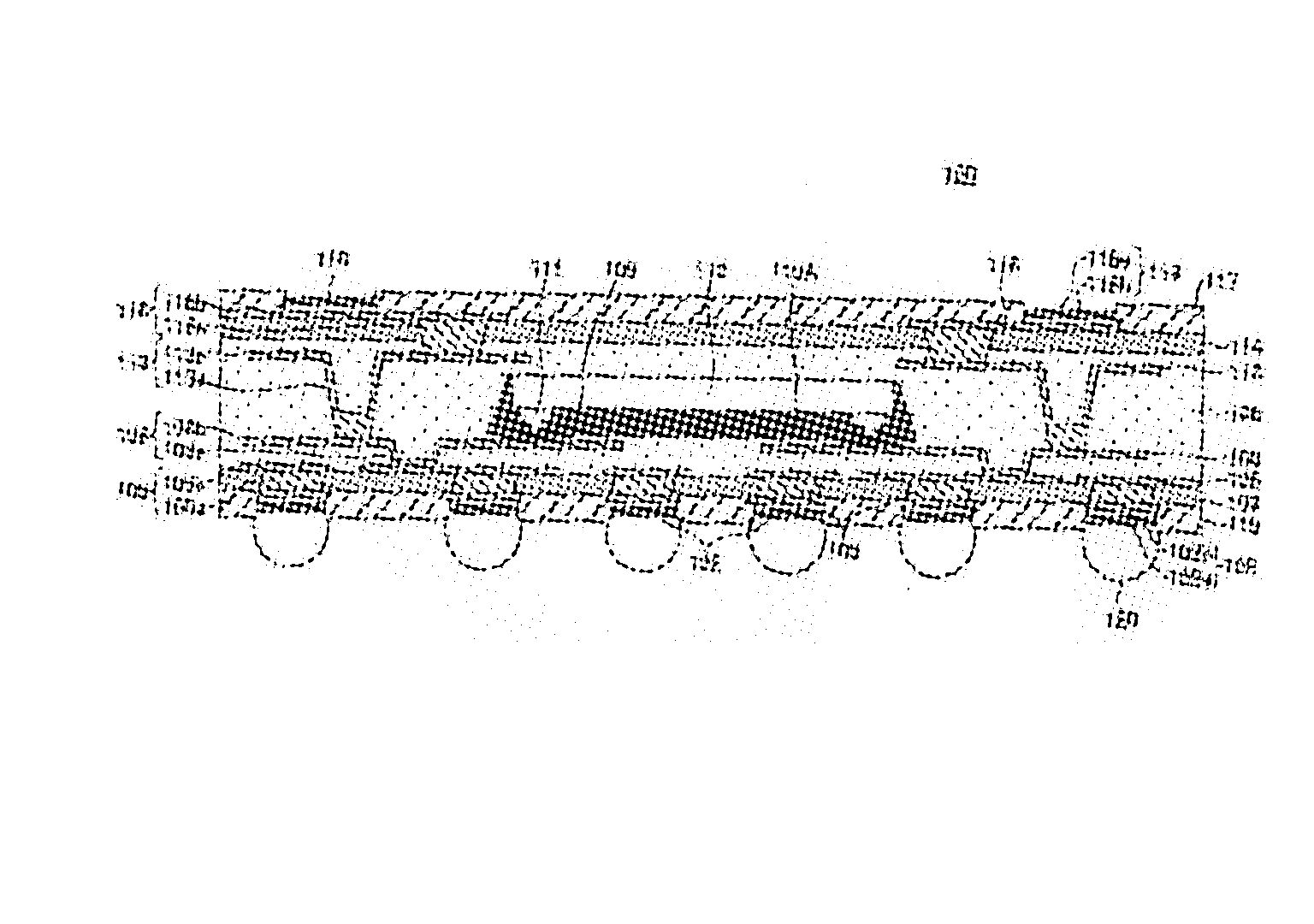
图1为通过本发明实施例的配线基板的制造方法制造的配线基板100的示意横截面视图。为了便于说明起见,在说明配线基板100的制造方法之前,首先说明配线基板100的结构。1 is a schematic cross-sectional view of a
如图1中所示,在本实施例中制造的配线基板100具有嵌入半导体芯片110的绝缘层106,该绝缘层包括例如环氧树脂等所谓增层树脂(buildup resin)材料。并且,相对于绝缘层106形成第一和第二加强层103、114。As shown in FIG. 1 , a
如图中所示,加强层103、114设置为从上部和底部将绝缘层106夹在它们之间。加强层103、114是用例如预浸渍材料等具有高刚度的材料形成的。绝缘层106由如前所述的挠性增层树脂材料构成。这样,通过设置用以将绝缘层106夹在其间的加强层103、114,绝缘层106通过加强层103、114而得以加强。As shown in the figure, the reinforcing
半导体芯片110连接到配线部(将在后面介绍),并通过该配线部连接到在阻焊层119中的开口中形成的电极102或阻焊层117中的开口中形成的电极118。电极102或118用于连接到例如母板、其他器件或连接器件等。The
在半导体芯片110的电极片(未示出)上,形成由例如金构成的柱形凸点111。柱形凸点111通过例如焊料连接部109连接到嵌入绝缘层106中的配线部108。从保护柱形凸点111和防止产生应力的观点出发,在半导体芯片110的下部形成底部填充层110A。On an electrode pad (not shown) of the
配线基板100具有配线部105、113、116以及配线部108。配线部105、108、113、116由例如铜构成。
配线部105包括导通塞105a和图案配线105b。导通塞105a形成在加强层103中形成的开口处。连接到导通塞105a的图案配线105b形成在加强层103上。The
配线部108形成在绝缘层106中。如图中所示,配线部108形成在配线部105的上方。配线部108包括在图案配线105b上形成的导通塞108a和连接到导通塞108a的图案配线108b。如前所述,半导体芯片110通过焊料连接部109和柱形凸点111连接到图案配线108b。The
配线部113形成在绝缘层106中。如图中所示,配线部113形成在配线部108的上方。配线部113电连接到配线部108。配线部113包括在图案配线108b上形成的导通塞113a和连接到导通塞113a的图案配线113b。The
如图中所示,在配线部113的上方形成配线部116。配线部116电连接到配线部113。配线部116包括在图案配线113b上形成的导通塞116a和连接到导通塞116a的图案配线116b。导通塞116a形成在加强层114中形成的开口处。图案配线116b形成在加强层114上。As shown in the drawing, a
在位于绝缘层106下方的阻焊层119中的开口处,形成连接到导通塞105a的电极102。在位于绝缘层106上方的阻焊层117的开口处,形成连接到导通塞116b的电极118。这样,配线基板100可以通过在顶部和底部的电极102、118提供到半导体芯片110的电连接。At the opening in the solder resist
阻焊层119、117是以覆盖加强层103和114的方式而形成的。在每个阻焊层119、117中,形成有用于形成电极102、118的开口。根据需要,在电极102上形成焊球120。也可以在电极118上形成焊球120。Solder resist
如此构造的配线基板100具有半导体芯片110和配线部105、108、113、116嵌入其中的绝缘层106,其中,一对加强层103、114将绝缘层106夹在它们之间。这样,即使当绝缘层106由挠性树脂材料制成时,也可以由具有高刚度的加强层103、114从两侧加强绝缘层106。这减少了配线基板100中的翘曲,可以给配线基板100提供高的平整度,并且可以应对精细设置的配线。
举例来说,优选的是用预浸渍材料形成加强层103、114。可以使用预浸渍材料作为用于形成多层配线基板(增层基板)的芯板材料。For example, it is preferred to form the reinforcing
举例来说,预浸渍材料具有用环氧树脂浸渍玻璃纤维的结构,并具有比一般增层树脂材料更高的热固化后刚度。例如,增层树脂材料的弹性模量(杨氏模量)为大约5GPa至8GPa,而预浸渍材料的弹性模量为20GPa或更高,这表明后者的刚度更高,从而可以减少配线基板中的翘曲。For example, prepregs have a structure in which glass fibers are impregnated with epoxy resin and have a higher post-heat cure stiffness than typical buildup resin materials. For example, the elastic modulus (Young's modulus) of the build-up resin material is about 5GPa to 8GPa, while the elastic modulus of the prepreg material is 20GPa or higher, which indicates that the latter is more rigid, which can reduce wiring. Warpage in the substrate.
用于加强层103、114的材料并不局限于预浸渍材料,而可以是具有高刚度的模制树脂。尽管优选的是在使用例如金属等导电材料的情况下,增加用以使配线部与加强层绝缘的结构,但是用于加强层103、114的材料可以是金属材料。可以基于允许配线基板100的薄型化设计的增层法,形成根据本实施例的配线基板100。The material used for the reinforcing
接下来,将参照图2至21,逐步说明配线基板的制造方法。Next, with reference to FIGS. 2 to 21 , a method of manufacturing the wiring board will be described step by step.
在图2中示出的工艺中,提供由例如铜等导电材料构成的200微米厚的支撑基板101。通过电镀法在支撑基板101上形成停止层121。停止层121为2至3微米厚的镍膜,并且是这样形成的:即,使用支撑基板101作为电极,通过电镀法在支撑基板101的顶面上形成该停止层。In the process shown in Figure 2, a 200 micron
在此时,对于上述电镀来说,是用支撑基板101作为通电路径。这样,支撑基板101优选为导电材料,或者更加优选为例如铜等低电阻材料。At this time, for the above-mentioned electroplating, the supporting
在图3中示出的工艺中,在形成停止层121的支撑基板101上形成图案配线105b。更确切地说,图案配线105b是这样形成的:即,通过光刻法形成抗蚀图案(未示出),将该抗蚀图案作为掩模,以通过电镀沉积铜,然后去除该抗蚀图案从而形成图案配线105b。In the process shown in FIG. 3 ,
接下来,在图4中示出的工艺中,在支撑基板101上形成绝缘层106,以便覆盖图案配线105b。绝缘层106由例如热固性环氧树脂等增层材料制成。用激光束在支撑基板101上形成的绝缘层106中形成导通孔106A,以便露出图案配线105b的一部分。Next, in the process shown in FIG. 4, an insulating
接下来,在图5中示出的工艺中,根据需要,在绝缘层106的表面上进行去污工艺,以去除导通孔中的残留物,并进行表面处理。接着,通过无电解电镀,在绝缘层106的表面和露出的图案配线105b的表面上形成由铜构成的种晶层(seed layer)107。Next, in the process shown in FIG. 5 , a desmear process is performed on the surface of the insulating
接下来,在图6中示出的工艺中,使用光刻法以形成抗蚀图案(未示出)。接下来,将抗蚀图案作为掩模,实施电解镀铜,从而在导通孔106A中形成导通塞108a,以及在绝缘层106上形成一体连接到导通塞108a的图案配线108b。导通塞108a和图案配线108b构成配线部108。当形成配线部108时,剥去抗蚀图案,并通过蚀刻去除露出的多余种晶层107。Next, in the process shown in FIG. 6, photolithography is used to form a resist pattern (not shown). Next, using the resist pattern as a mask, electrolytic copper plating is performed to form via
接下来,在图7中示出的工艺中,在绝缘层106上形成绝缘层106a,以便覆盖配线部108。绝缘层106a由例如热固性环氧树脂等的增层材料制成,即与绝缘层106的材料相同。这样,绝缘层106a和绝缘层106实质上成为一体。在图7中及以后示出的工艺中,假定绝缘层106包括绝缘层106a。Next, in the process shown in FIG. 7 , insulating layer 106 a is formed on insulating
接下来,在图8中示出的工艺中,通过使用激光束加工方法,在绝缘层106中形成开口106B,以便露出配线部108的一部分(导通塞108a)。接下来,根据需要,向绝缘层106施加去污工艺,以去除开口中的残留物,并进行表面处理。此后,如图9中所示,使用电镀法以在开口106B处形成焊料连接部109。Next, in the process shown in FIG. 8 , by using a laser beam processing method, an opening 106B is formed in the insulating
接下来,在图10中示出的工艺中,执行将半导体芯片110安装在绝缘层106上的工艺。半导体芯片110具有预先在其上形成的由金构成的柱形凸点111。在半导体芯片110上,柱形凸点111和焊料连接部109定位为互相对应,并通过倒装芯片法连接到配线部108(图案配线108b)上。在此时,在半导体芯片110和绝缘层106之间形成底部填充层110A。Next, in the process shown in FIG. 10 , a process of mounting the
接下来,在图11中示出的工艺中,在绝缘层106上形成绝缘层106b,以便覆盖半导体芯片110。绝缘层106b由例如热固性环氧树脂等的增层材料制成。绝缘层106b和绝缘层106实质上成为一体。在图11中及以后示出的工艺中,假定绝缘层106包括绝缘层106b。Next, in the process shown in FIG. 11 , an insulating
接下来,在图12中示出的工艺中,在绝缘层106中形成导通孔106C。导通孔106C是这样形成的:即,通过例如使用激光束加工方法,以露出图案配线108b的方式形成的。接下来,根据需要,在绝缘层106的表面上施加去污工艺,从而去除导通孔中的残留物,并进行表面处理。Next, in the process shown in FIG. 12 , via holes 106C are formed in insulating
接下来,通过无电解电镀法,在绝缘层106的表面上和图案配线108b的表面上形成由铜构成的种晶层112。种晶层112通过配线部108、图案配线105b和由镍构成的停止层121电连接到由铜构成的支撑基板101上。Next, the seed layer 112 made of copper is formed on the surface of the insulating
接下来,在图13中示出的工艺中,使用光刻法形成抗蚀图案(未示出)。接下来,将抗蚀图案作为掩模以实施电解镀铜,从而在导通孔106C中形成导通塞113a,以及在绝缘层106上形成连接到导通塞113a的图案配线113b。导通塞113a和图案配线113b构成配线部113。当形成配线部113时,剥去抗蚀图案,并通过蚀刻去除露出的多余种晶层。Next, in the process shown in FIG. 13, a resist pattern (not shown) is formed using photolithography. Next, electrolytic copper plating is performed using the resist pattern as a mask, thereby forming a via
接下来,在图14中示出的工艺中,在绝缘层106上形成由例如热固性环氧树脂构成的绝缘层(增层)106c,以便覆盖配线部108。绝缘层106c和绝缘层106实质上成为一体。在图14中及以后示出的工艺中,假定绝缘层106包括绝缘层106c。Next, in the process shown in FIG. 14 , an insulating layer (build-up layer) 106 c made of, for example, a thermosetting epoxy resin is formed on the insulating
在前述各个工艺中,进行在支撑基板101上层压绝缘层106、图案配线105b和配线部108、113的工艺。在此时,绝缘层106由具有较小弹性模量、并在其中装填有致密填料的树脂材料制成,该树脂材料不太可能在该绝缘层中产生翘曲。这样,在图2至14中示出的工艺中,不会发生问题性翘曲。In the aforementioned respective processes, a process of laminating the insulating
接下来,在图15中示出的工艺中,通过蚀刻去除支撑基板101。所使用的蚀刻液应该溶解支撑基板101(铜),而不应溶解停止层121的镍。这使得停止层121停止支撑基板101的去除,从而防止蚀刻液对停止层121内侧的层(即绝缘层106、图案配线105b和配线部108、113)产生影响。另外,使去除支撑基板101过程中的去除处理管理变得容易,从而简化了配线基板100的制造。当完成支撑基板101的去除时,用溶解镍而不会溶解铜的蚀刻液去除停止层121。Next, in the process shown in FIG. 15 , the supporting
去除支撑基板101,意味着没有任何部件支撑绝缘层106。当去除支撑基板101时,绝缘层106为大约200至300微米厚,这保证了承受处理的刚度。支撑基板101的缺少不会成为后面所述的图16中及以后示出的工艺的障碍。The removal of the
接下来,在图16中示出的工艺中,在绝缘层106的下方形成加强层103,同时在绝缘层106的上方形成加强层114。这样,加强层103和114将绝缘层106夹在它们之间。Next, in the process shown in FIG. 16 , reinforcing
这里,同时形成加强层103和114。这意味着同时进行加强层103和114的固化,以便从绝缘层106等的上方和下方均匀施加加强层103和114在固化时产生的收缩,从而防止配线基板可能的翘曲。此外,通过同时进行固化,加强层103的热历程和加强层114的热历程可以是相同的。Here, the reinforcement layers 103 and 114 are formed simultaneously. This means that the curing of the reinforcement layers 103 and 114 is performed simultaneously so that the shrinkage of the reinforcement layers 103 and 114 during curing is uniformly applied from above and below the insulating
在这种情况下,暂时将加强层103和114挤压并附着到绝缘层106上,然后进行固化。加强层103和114可以分别或同时附着到绝缘层106上。In this case, the reinforcing
通过例如在热量和压力下层压预浸渍材料来形成加强层103、114。预浸渍材料具有用如前所述的环氧树脂浸渍玻璃纤维的结构,并具有比一般增层树脂材料更高的热固化后刚度。例如,增层树脂材料的弹性模量(杨氏模量)为大约5GPa至8GPa,而预浸渍材料的弹性模量为20GPa或更高,这表明后者的刚度更高,从而可以减少配线基板中的翘曲。The reinforcement layers 103, 114 are formed by laminating prepreg materials, for example under heat and pressure. Prepregs have a structure in which glass fibers are impregnated with epoxy resin as described above, and have a higher stiffness after heat curing than general buildup resin materials. For example, the elastic modulus (Young's modulus) of the build-up resin material is about 5GPa to 8GPa, while the elastic modulus of the prepreg material is 20GPa or higher, which indicates that the latter is more rigid, which can reduce wiring. Warpage in the substrate.
接下来,在图17中示出的工艺中,通过使用激光束在加强层103中形成导通孔103A,以便露出图案配线105b。然后,通过使用激光束在加强层114和绝缘层106中形成导通孔114A,以便露出配线部113(图案配线113b)。其中,导通孔103A和114A是同时形成的。Next, in the process shown in FIG. 17 , a via
接下来,在图18中示出的工艺中,为了去除导通孔中的残留物并进行表面处理,根据需要,向加强层103的底面和加强层114的顶面施加去污工艺。然后,通过无电解电镀法,分别在加强层103的底面和加强层114的顶面(包括绝缘层106从导通孔114A露出的一部分)上形成由铜构成的种晶层104、115。其中,种晶层104和115是同时形成的。Next, in the process shown in FIG. 18 , a desmear process is applied to the bottom surface of the
接下来,在图19中示出的工艺中,使用光刻法在种晶层104和种晶层115中形成抗蚀图案(未示出)。接下来,将抗蚀图案作为掩模,以实施电解镀铜,从而在加强层103上形成导通塞105a,以便提供到图案配线105b的连接。导通塞105a和图案配线105b构成配线部105。Next, in the process shown in FIG. 19, a resist pattern (not shown) is formed in the
同时,将抗蚀图案作为掩模以实施电解镀铜从而形成导通塞116a,以便提供到从加强层114中形成的导通孔114A露出的图案配线113b的连接。在加强层114上形成图案配线116b,以提供到导通塞116a的连接。导通塞116a和图案配线116b构成配线部116。At the same time, electrolytic copper plating is performed using the resist pattern as a mask to form a via
在形成配线部105、116之后,剥去抗蚀图案,并通过蚀刻去除露出的多余种晶层104、115。After the
接下来,在图20中示出的工艺中,形成阻焊层119以覆盖加强层103,并且在阻焊层119中使配线部105(导通塞105a)露出的预定位置处形成开口119A。形成阻焊层117以便覆盖加强层114。在阻焊层117中使配线部116(图案配线116b)露出的预定位置处形成开口117A。其中,包括开口117A的阻焊层117和包括开口119A的阻焊层119是同时形成的。Next, in the process shown in FIG. 20 , a solder resist
接下来,在图21中示出的工艺中,在从开口117A露出的配线部116(图案配线116b)上形成包括例如金层118a和镍层118b的电极118。在从开口119A露出的配线部105(导通塞105a)上形成包括例如金层102a和镍层102b的电极102(表面处理)。其中,电极102和电极118是同时形成的。Next, in the process shown in FIG. 21 ,
此后,在电极102上形成焊球120,从而形成图1示出的配线基板100。Thereafter,
以上制造方法为使用无芯结构(去除支撑基板的结构)的增层法。此方法可以实现配线基板的薄型化、紧凑和轻质设计。加强层103、114的使用减少了配线基板中的翘曲。这使得形成包括超精细配线部的薄型化配线基板成为可能。The above manufacturing method is a build-up method using a coreless structure (a structure in which a support substrate is removed). This method enables thinning, compact and lightweight design of the wiring board. The use of the reinforcement layers 103, 114 reduces warpage in the wiring substrate. This makes it possible to form a thinned wiring board including ultrafine wiring portions.
在本实施例中,形成嵌入有半导体芯片110的配线部116和配线部105、108、113,然后去除支撑基板101。同时形成加强层103和114,以将其上未附着支撑基板101的绝缘层106夹在加强层103和114之间。通常,每个加强层103、114在固化时会表现出较大收缩。通过同时形成加强层103和114,以将绝缘层106、配线部116等夹在加强层103和114之间,这样,从绝缘层106、配线部116等的上方和下方均匀施加固化时产生的收缩,从而防止可能的翘曲。In the present embodiment, the
根据本实施例,在去除支撑基板101之后的工艺中,更具体来说,在图15至21中示出的工艺中,同时进行图中所示的在绝缘层106的顶面上的处理和底面上的处理。这样,在去除支撑基板101之后,同时在绝缘层106的顶面和底面形成各层,从而简化了制造工艺,并减少了制造所需的时间。According to the present embodiment, in the process after removing the supporting
虽然已经参照优选实施例对本发明进行了说明,但是本发明并不局限于这些具体实施例,而是在未背离权利要求书的情况下,可以对本发明做出变型和变更。Although the invention has been described with reference to preferred embodiments, the invention is not limited to these specific embodiments, but modifications and changes may be made to the invention without departing from the claims.
显然,对于所属领域的技术人员来说,在未背离本发明的要旨或保护范围的情况下,可以对本发明所述优选实施例做出各种修改和变型。因而,本发明旨在涵盖与所附的权利要求书及其等效内容所限定的保护范围一致的本发明的所有修改和变型。Obviously, those skilled in the art can make various modifications and variations to the preferred embodiments of the present invention without departing from the gist or protection scope of the present invention. Accordingly, it is intended that the present invention cover all modifications and variations of this invention coming within the scope of protection as defined by the appended claims and their equivalents.
本申请基于2005年8月26日提交的日本专利申请No.2005-246438,并要求该申请的外国优先权,其内容在此通过引用的方式并入本文。This application is based on and claims foreign priority from Japanese Patent Application No. 2005-246438 filed on August 26, 2005, the contents of which are hereby incorporated by reference.
Claims (5)
Applications Claiming Priority (3)
| Application Number | Priority Date | Filing Date | Title |
|---|---|---|---|
| JP2005-246438 | 2005-08-26 | ||
| JP2005246438 | 2005-08-26 | ||
| JP2005246438A JP2007059821A (en) | 2005-08-26 | 2005-08-26 | Wiring board manufacturing method |
Publications (2)
| Publication Number | Publication Date |
|---|---|
| CN1921079A true CN1921079A (en) | 2007-02-28 |
| CN1921079B CN1921079B (en) | 2010-07-28 |
Family
ID=37607615
Family Applications (1)
| Application Number | Title | Priority Date | Filing Date |
|---|---|---|---|
| CN2006101099819A Active CN1921079B (en) | 2005-08-26 | 2006-08-25 | Manufacturing method of wiring board |
Country Status (6)
| Country | Link |
|---|---|
| US (1) | US7937828B2 (en) |
| EP (1) | EP1758438A3 (en) |
| JP (1) | JP2007059821A (en) |
| KR (1) | KR20070024374A (en) |
| CN (1) | CN1921079B (en) |
| TW (1) | TW200717672A (en) |
Cited By (12)
| Publication number | Priority date | Publication date | Assignee | Title |
|---|---|---|---|---|
| CN101221908B (en) * | 2008-01-29 | 2010-10-13 | 日月光半导体制造股份有限公司 | Substrate process with bump and structure thereof |
| CN102067281A (en) * | 2008-04-25 | 2011-05-18 | 株式会社半导体能源研究所 | Semiconductor device and method for manufacturing the same |
| CN101515574B (en) * | 2008-02-18 | 2011-06-22 | 旭德科技股份有限公司 | Chip package carrier board, chip package body and manufacturing method thereof |
| US7999380B2 (en) | 2007-06-07 | 2011-08-16 | Advanced Semiconductor Engineering, Inc. | Process for manufacturing substrate with bumps and substrate structure |
| CN103107146A (en) * | 2011-10-04 | 2013-05-15 | 三星电子株式会社 | Semiconductor package and method of manufacturing the same |
| CN103383927A (en) * | 2012-05-03 | 2013-11-06 | 三星电子株式会社 | Semiconductor encapsulation and forming method thereof |
| CN104684254A (en) * | 2013-11-27 | 2015-06-03 | Tdk株式会社 | IC embedded substrate and method of manufacturing the same |
| CN106982508A (en) * | 2016-01-18 | 2017-07-25 | 三星电子株式会社 | Printed circuit board (PCB) and the semiconductor packages including the printed circuit board (PCB) |
| CN107104070A (en) * | 2016-02-19 | 2017-08-29 | 三星电子株式会社 | Support substrate and the method that semiconductor package part is manufactured using support substrate |
| CN107799281A (en) * | 2016-08-30 | 2018-03-13 | 三星电机株式会社 | Inductor and method for manufacturing inductor |
| TWI771273B (en) * | 2015-07-03 | 2022-07-21 | 日商安靠科技日本公司 | Semiconductor device and method for manufacturing same |
| CN115274468A (en) * | 2021-11-11 | 2022-11-01 | 天芯互联科技有限公司 | Chip packaging method and packaging mechanism |
Families Citing this family (48)
| Publication number | Priority date | Publication date | Assignee | Title |
|---|---|---|---|---|
| EP1970951A3 (en) * | 2007-03-13 | 2009-05-06 | Semiconductor Energy Laboratory Co., Ltd. | Semiconductor device and manufacturing method thereof |
| US7960210B2 (en) | 2007-04-23 | 2011-06-14 | Cufer Asset Ltd. L.L.C. | Ultra-thin chip packaging |
| EP2001047A1 (en) * | 2007-06-07 | 2008-12-10 | Semiconductor Energy Laboratory Co, Ltd. | Semiconductor device |
| EP2019425A1 (en) * | 2007-07-27 | 2009-01-28 | Semiconductor Energy Laboratory Co., Ltd. | Semiconductor device and method for manufacturing the same |
| KR101354372B1 (en) * | 2007-07-31 | 2014-01-23 | 삼성전자주식회사 | Reinforce for printed circuit board and integrated circuit package using the same |
| WO2009031482A1 (en) * | 2007-09-07 | 2009-03-12 | Semiconductor Energy Laboratory Co., Ltd. | Semiconductor device and method for manufacturing the same |
| JP5096855B2 (en) * | 2007-09-27 | 2012-12-12 | 新光電気工業株式会社 | Wiring board manufacturing method and wiring board |
| WO2009139282A1 (en) | 2008-05-12 | 2009-11-19 | Semiconductor Energy Laboratory Co., Ltd. | Semiconductor device and method for manufacturing semiconductor device |
| EP2297778A1 (en) * | 2008-05-23 | 2011-03-23 | Semiconductor Energy Laboratory Co, Ltd. | Semiconductor device |
| WO2009142310A1 (en) * | 2008-05-23 | 2009-11-26 | Semiconductor Energy Laboratory Co., Ltd. | Semiconductor device and method for manufacturing the same |
| JP5248412B2 (en) | 2008-06-06 | 2013-07-31 | 株式会社半導体エネルギー研究所 | Method for manufacturing semiconductor device |
| US8053253B2 (en) * | 2008-06-06 | 2011-11-08 | Semiconductor Energy Laboratory Co., Ltd. | Method for manufacturing semiconductor device |
| US8598719B2 (en) | 2008-06-12 | 2013-12-03 | Sumitomo Bakelite Company Limited | Semiconductor element mounting board |
| KR100996914B1 (en) * | 2008-06-19 | 2010-11-26 | 삼성전기주식회사 | Chip embedded printed circuit board and its manufacturing method |
| TWI475282B (en) | 2008-07-10 | 2015-03-01 | Semiconductor Energy Lab | Liquid crystal display device and method for manufacturing the same |
| KR101925772B1 (en) | 2008-07-10 | 2018-12-06 | 가부시키가이샤 한도오따이 에네루기 켄큐쇼 | Light emitting device and electronic device |
| TWI401000B (en) * | 2008-07-23 | 2013-07-01 | 日本電氣股份有限公司 | Coreless wiring board, semiconductor device and method of manufacturing same |
| JP5216716B2 (en) | 2008-08-20 | 2013-06-19 | 株式会社半導体エネルギー研究所 | Light emitting device and manufacturing method thereof |
| WO2010032602A1 (en) | 2008-09-18 | 2010-03-25 | Semiconductor Energy Laboratory Co., Ltd. | Semiconductor device |
| WO2010032611A1 (en) | 2008-09-19 | 2010-03-25 | Semiconductor Energy Laboratory Co., Ltd. | Semiconductor device and method for manufacturing the same |
| WO2010038599A1 (en) * | 2008-10-01 | 2010-04-08 | Semiconductor Energy Laboratory Co., Ltd. | Semiconductor device |
| JP5147678B2 (en) * | 2008-12-24 | 2013-02-20 | 新光電気工業株式会社 | Manufacturing method of fine wiring package |
| JP5339928B2 (en) * | 2009-01-15 | 2013-11-13 | 新光電気工業株式会社 | Wiring board and manufacturing method thereof |
| JPWO2010101167A1 (en) * | 2009-03-05 | 2012-09-10 | 日本電気株式会社 | Semiconductor device and manufacturing method thereof |
| KR20110039879A (en) * | 2009-10-12 | 2011-04-20 | 삼성전기주식회사 | Electronic component embedded printed circuit board and manufacturing method |
| WO2011089936A1 (en) * | 2010-01-22 | 2011-07-28 | 日本電気株式会社 | Substrate with built-in functional element, and wiring substrate |
| TWI420996B (en) * | 2010-07-30 | 2013-12-21 | Lg伊諾特股份有限公司 | Printed circuit board and method of manufacturing same |
| EP2448378A1 (en) * | 2010-10-26 | 2012-05-02 | ATOTECH Deutschland GmbH | Composite build-up materials for embedding of active components |
| JP2013211518A (en) * | 2012-02-28 | 2013-10-10 | Ngk Spark Plug Co Ltd | Multilayer wiring board and manufacturing method of the same |
| JP5981232B2 (en) * | 2012-06-06 | 2016-08-31 | 新光電気工業株式会社 | Semiconductor package, semiconductor device, and semiconductor package manufacturing method |
| JP6092555B2 (en) * | 2012-09-24 | 2017-03-08 | 新光電気工業株式会社 | Wiring board manufacturing method |
| JP6478309B2 (en) * | 2012-12-31 | 2019-03-06 | サムソン エレクトロ−メカニックス カンパニーリミテッド. | Multilayer substrate and method for manufacturing multilayer substrate |
| TWI509749B (en) * | 2013-05-20 | 2015-11-21 | 矽品精密工業股份有限公司 | Semiconductor package manufacturing method |
| KR102250997B1 (en) | 2014-05-02 | 2021-05-12 | 삼성전자주식회사 | Semiconductor package |
| US20150366081A1 (en) * | 2014-06-15 | 2015-12-17 | Unimicron Technology Corp. | Manufacturing method for circuit structure embedded with electronic device |
| US9704735B2 (en) * | 2014-08-19 | 2017-07-11 | Intel Corporation | Dual side solder resist layers for coreless packages and packages with an embedded interconnect bridge and their methods of fabrication |
| JP6358431B2 (en) | 2014-08-25 | 2018-07-18 | 新光電気工業株式会社 | Electronic component device and manufacturing method thereof |
| TWI623251B (en) * | 2014-08-29 | 2018-05-01 | 恆勁科技股份有限公司 | Intermediary substrate manufacturing method |
| JP2016054188A (en) * | 2014-09-03 | 2016-04-14 | 大日本印刷株式会社 | Component built-in wiring board, component built-in wiring board manufacturing method, and intermediate wiring layer for component built-in wiring board manufacturing |
| TWI582861B (en) * | 2014-09-12 | 2017-05-11 | 矽品精密工業股份有限公司 | Encapsulation structure of embedded component and its preparation method |
| US9941219B2 (en) | 2014-09-19 | 2018-04-10 | Intel Corporation | Control of warpage using ABF GC cavity for embedded die package |
| JP6451569B2 (en) * | 2015-09-14 | 2019-01-16 | 株式会社デンソー | Electronic equipment |
| US10276467B2 (en) * | 2016-03-25 | 2019-04-30 | Samsung Electro-Mechanics Co., Ltd. | Fan-out semiconductor package |
| KR101999625B1 (en) * | 2016-03-25 | 2019-07-17 | 삼성전자주식회사 | Fan-out semiconductor package |
| US9853011B2 (en) | 2016-03-29 | 2017-12-26 | Advanced Semiconductor Engineering, Inc. | Semiconductor package structure and method for manufacturing the same |
| US11432402B2 (en) * | 2018-10-11 | 2022-08-30 | Microchip Technology Caldicot Limited | Flipped-conductor-patch lamination for ultra fine-line substrate creation |
| JP7211757B2 (en) * | 2018-10-22 | 2023-01-24 | 新光電気工業株式会社 | wiring board |
| US10847400B2 (en) * | 2018-12-28 | 2020-11-24 | Applied Materials, Inc. | Adhesive-less substrate bonding to carrier plate |
Family Cites Families (16)
| Publication number | Priority date | Publication date | Assignee | Title |
|---|---|---|---|---|
| JPH09139560A (en) | 1995-11-14 | 1997-05-27 | Toshiba Corp | Circuit board device and manufacturing method thereof |
| JP3635219B2 (en) | 1999-03-11 | 2005-04-06 | 新光電気工業株式会社 | Multilayer substrate for semiconductor device and manufacturing method thereof |
| JP2002076637A (en) | 2000-08-29 | 2002-03-15 | Matsushita Electric Ind Co Ltd | Chip component built-in substrate and manufacturing method thereof |
| JP3760101B2 (en) * | 2001-02-13 | 2006-03-29 | 富士通株式会社 | Multilayer printed wiring board and manufacturing method thereof |
| TW558743B (en) * | 2001-08-22 | 2003-10-21 | Semiconductor Energy Lab | Peeling method and method of manufacturing semiconductor device |
| KR100516795B1 (en) * | 2001-10-31 | 2005-09-26 | 신꼬오덴기 고교 가부시키가이샤 | Method for manufacturing multilayer circuit board for semiconductor device |
| JP3492348B2 (en) * | 2001-12-26 | 2004-02-03 | 新光電気工業株式会社 | Method of manufacturing package for semiconductor device |
| TW200302685A (en) * | 2002-01-23 | 2003-08-01 | Matsushita Electric Industrial Co Ltd | Circuit component built-in module and method of manufacturing the same |
| JP2004079773A (en) * | 2002-08-19 | 2004-03-11 | Taiyo Yuden Co Ltd | Multilayer printed wiring substrate and its production method |
| US7394663B2 (en) | 2003-02-18 | 2008-07-01 | Matsushita Electric Industrial Co., Ltd. | Electronic component built-in module and method of manufacturing the same |
| JP2004327624A (en) | 2003-04-23 | 2004-11-18 | Shinko Electric Ind Co Ltd | Multi-layer circuit board with built-in components |
| JP4183708B2 (en) | 2003-07-04 | 2008-11-19 | 株式会社村田製作所 | Manufacturing method of component-embedded substrate |
| CN1577819A (en) * | 2003-07-09 | 2005-02-09 | 松下电器产业株式会社 | Circuit board with in-built electronic component and method for manufacturing the same |
| JP3904541B2 (en) * | 2003-09-26 | 2007-04-11 | 沖電気工業株式会社 | Manufacturing method of semiconductor device embedded substrate |
| US6974724B2 (en) * | 2004-04-28 | 2005-12-13 | Nokia Corporation | Shielded laminated structure with embedded chips |
| US20060085058A1 (en) * | 2004-10-20 | 2006-04-20 | Rosenthal Arthur L | System and method for delivering a biologically active material to a body lumen |
-
2005
- 2005-08-26 JP JP2005246438A patent/JP2007059821A/en active Pending
-
2006
- 2006-08-22 KR KR1020060079178A patent/KR20070024374A/en not_active Withdrawn
- 2006-08-25 TW TW095131357A patent/TW200717672A/en unknown
- 2006-08-25 CN CN2006101099819A patent/CN1921079B/en active Active
- 2006-08-25 EP EP06017783A patent/EP1758438A3/en not_active Withdrawn
- 2006-08-25 US US11/509,684 patent/US7937828B2/en active Active
Cited By (24)
| Publication number | Priority date | Publication date | Assignee | Title |
|---|---|---|---|---|
| US7999380B2 (en) | 2007-06-07 | 2011-08-16 | Advanced Semiconductor Engineering, Inc. | Process for manufacturing substrate with bumps and substrate structure |
| CN101221908B (en) * | 2008-01-29 | 2010-10-13 | 日月光半导体制造股份有限公司 | Substrate process with bump and structure thereof |
| CN101515574B (en) * | 2008-02-18 | 2011-06-22 | 旭德科技股份有限公司 | Chip package carrier board, chip package body and manufacturing method thereof |
| US8637932B2 (en) | 2008-04-25 | 2014-01-28 | Semiconductor Energy Laboratory Co., Ltd. | Semiconductor device and method for manufacturing the same |
| CN102067281A (en) * | 2008-04-25 | 2011-05-18 | 株式会社半导体能源研究所 | Semiconductor device and method for manufacturing the same |
| CN102067281B (en) * | 2008-04-25 | 2013-06-12 | 株式会社半导体能源研究所 | Semiconductor device and method for manufacturing the same |
| US9171808B2 (en) | 2008-04-25 | 2015-10-27 | Semiconductor Energy Laboratory Co., Ltd. | Semiconductor device and method for manufacturing the same |
| CN103107146A (en) * | 2011-10-04 | 2013-05-15 | 三星电子株式会社 | Semiconductor package and method of manufacturing the same |
| CN103107146B (en) * | 2011-10-04 | 2017-01-18 | 三星电子株式会社 | Semiconductor package and method of manufacturing the same |
| CN103383927A (en) * | 2012-05-03 | 2013-11-06 | 三星电子株式会社 | Semiconductor encapsulation and forming method thereof |
| CN104684254A (en) * | 2013-11-27 | 2015-06-03 | Tdk株式会社 | IC embedded substrate and method of manufacturing the same |
| CN104684254B (en) * | 2013-11-27 | 2017-12-19 | Tdk株式会社 | IC built-in substrates and its manufacture method |
| TWI771273B (en) * | 2015-07-03 | 2022-07-21 | 日商安靠科技日本公司 | Semiconductor device and method for manufacturing same |
| CN106982508A (en) * | 2016-01-18 | 2017-07-25 | 三星电子株式会社 | Printed circuit board (PCB) and the semiconductor packages including the printed circuit board (PCB) |
| US10672694B2 (en) | 2016-01-18 | 2020-06-02 | Samsung Electronics Co., Ltd. | Printed circuit board, semiconductor package including the printed circuit board, and method of manufacturing the printed circuit board |
| CN106982508B (en) * | 2016-01-18 | 2019-11-08 | 三星电子株式会社 | Printed circuit board and semiconductor package including the printed circuit board |
| CN107104070A (en) * | 2016-02-19 | 2017-08-29 | 三星电子株式会社 | Support substrate and the method that semiconductor package part is manufactured using support substrate |
| CN107104070B (en) * | 2016-02-19 | 2020-11-17 | 三星电子株式会社 | Supporting substrate and method of manufacturing semiconductor package using the same |
| US10763031B2 (en) | 2016-08-30 | 2020-09-01 | Samsung Electro-Mechanics Co., Ltd. | Method of manufacturing an inductor |
| CN112071586A (en) * | 2016-08-30 | 2020-12-11 | 三星电机株式会社 | Inductor and method of manufacturing the same |
| CN107799281A (en) * | 2016-08-30 | 2018-03-13 | 三星电机株式会社 | Inductor and method for manufacturing inductor |
| US11600430B2 (en) | 2016-08-30 | 2023-03-07 | Samsung Electro-Mechanics Co., Ltd. | Inductor including high-rigidity insulating layers |
| CN112071586B (en) * | 2016-08-30 | 2024-10-01 | 三星电机株式会社 | Inductor and method for manufacturing the same |
| CN115274468A (en) * | 2021-11-11 | 2022-11-01 | 天芯互联科技有限公司 | Chip packaging method and packaging mechanism |
Also Published As
| Publication number | Publication date |
|---|---|
| KR20070024374A (en) | 2007-03-02 |
| EP1758438A2 (en) | 2007-02-28 |
| JP2007059821A (en) | 2007-03-08 |
| US7937828B2 (en) | 2011-05-10 |
| EP1758438A3 (en) | 2009-02-25 |
| US20070044303A1 (en) | 2007-03-01 |
| CN1921079B (en) | 2010-07-28 |
| TW200717672A (en) | 2007-05-01 |
Similar Documents
| Publication | Publication Date | Title |
|---|---|---|
| CN1921079A (en) | Method of manufacturing a wiring board | |
| CN1929123A (en) | Multilayered wiring substrate and method of manufacturing the same | |
| CN100343965C (en) | Semiconductor device having conducting portion of upper and lower conductive layers, and method of fabricating the same | |
| JP5195422B2 (en) | Wiring board, mounting board, and electronic device | |
| CN1835661A (en) | Wiring board manufacturing method | |
| CN1882224B (en) | Wiring substrate and manufacturing method thereof | |
| CN1835654A (en) | Wiring board and method of manufacturing the same | |
| CN1481658A (en) | method for manufacturing multilayer circuit board for semiconductor device | |
| US20110010932A1 (en) | Wiring board, semiconductor device having wiring board, and method of manufacturing wiring board | |
| CN1649139A (en) | Semiconductor device and method of fabricating the same | |
| CN1619787A (en) | Semiconductor device | |
| CN1266752C (en) | Manufacturing method of circuit device | |
| CN1519920A (en) | Semiconductor device and method for manufacturing semiconductor device | |
| CN101076883A (en) | Structure and method for fabricating interconnection elements, including multilayer wiring boards for interconnection elements | |
| CN1723556A (en) | Semiconductor package having semiconductor constructing body and method of manufacturing the same | |
| CN1282983A (en) | Manufacturing method of semiconductor device | |
| CN1779971A (en) | Semiconductor device and method for producing the same | |
| CN1941339A (en) | Semiconductor IC-embedded substrate and method for manufacturing same | |
| CN1798479A (en) | Printed circuit board including embedded chips and method of fabricating the same | |
| CN1337145A (en) | Multi-layered printed wiring board and prodn. method thereof | |
| CN1191619C (en) | Circuit device and its producing method | |
| CN1672473A (en) | Method for manufacturing board with built-in device and board with built-in device, and method for manufacturing printed wiring board and printed wiring board | |
| CN1521842A (en) | Mounted body of electronic component and manufacturing method thereof | |
| CN1317759C (en) | Manufacturing method of printed circuit board, semiconductor package, base insulating film, and interconnection substrate | |
| CN1254856C (en) | Manufacturing method of circuit device |
Legal Events
| Date | Code | Title | Description |
|---|---|---|---|
| C06 | Publication | ||
| PB01 | Publication | ||
| C10 | Entry into substantive examination | ||
| SE01 | Entry into force of request for substantive examination | ||
| C14 | Grant of patent or utility model | ||
| GR01 | Patent grant |