CN1905135B - Plasma etching apparatus - Google Patents
Plasma etching apparatus Download PDFInfo
- Publication number
- CN1905135B CN1905135B CN2006101039752A CN200610103975A CN1905135B CN 1905135 B CN1905135 B CN 1905135B CN 2006101039752 A CN2006101039752 A CN 2006101039752A CN 200610103975 A CN200610103975 A CN 200610103975A CN 1905135 B CN1905135 B CN 1905135B
- Authority
- CN
- China
- Prior art keywords
- substrate
- chamber
- plasma
- etching apparatus
- shielding
- Prior art date
- Legal status (The legal status is an assumption and is not a legal conclusion. Google has not performed a legal analysis and makes no representation as to the accuracy of the status listed.)
- Active
Links
Images


Classifications
-
- H—ELECTRICITY
- H01—ELECTRIC ELEMENTS
- H01J—ELECTRIC DISCHARGE TUBES OR DISCHARGE LAMPS
- H01J37/00—Discharge tubes with provision for introducing objects or material to be exposed to the discharge, e.g. for the purpose of examination or processing thereof
- H01J37/32—Gas-filled discharge tubes
- H01J37/32009—Arrangements for generation of plasma specially adapted for examination or treatment of objects, e.g. plasma sources
- H01J37/32082—Radio frequency generated discharge
- H01J37/321—Radio frequency generated discharge the radio frequency energy being inductively coupled to the plasma
-
- H—ELECTRICITY
- H10—SEMICONDUCTOR DEVICES; ELECTRIC SOLID-STATE DEVICES NOT OTHERWISE PROVIDED FOR
- H10P—GENERIC PROCESSES OR APPARATUS FOR THE MANUFACTURE OR TREATMENT OF DEVICES COVERED BY CLASS H10
- H10P50/00—Etching of wafers, substrates or parts of devices
- H10P50/20—Dry etching; Plasma etching; Reactive-ion etching
- H10P50/24—Dry etching; Plasma etching; Reactive-ion etching of semiconductor materials
- H10P50/242—Dry etching; Plasma etching; Reactive-ion etching of semiconductor materials of Group IV materials
-
- H—ELECTRICITY
- H01—ELECTRIC ELEMENTS
- H01J—ELECTRIC DISCHARGE TUBES OR DISCHARGE LAMPS
- H01J37/00—Discharge tubes with provision for introducing objects or material to be exposed to the discharge, e.g. for the purpose of examination or processing thereof
- H01J37/32—Gas-filled discharge tubes
- H01J37/32431—Constructional details of the reactor
- H01J37/3244—Gas supply means
-
- H—ELECTRICITY
- H01—ELECTRIC ELEMENTS
- H01J—ELECTRIC DISCHARGE TUBES OR DISCHARGE LAMPS
- H01J37/00—Discharge tubes with provision for introducing objects or material to be exposed to the discharge, e.g. for the purpose of examination or processing thereof
- H01J37/32—Gas-filled discharge tubes
- H01J37/32431—Constructional details of the reactor
- H01J37/3244—Gas supply means
- H01J37/32449—Gas control, e.g. control of the gas flow
-
- H—ELECTRICITY
- H01—ELECTRIC ELEMENTS
- H01J—ELECTRIC DISCHARGE TUBES OR DISCHARGE LAMPS
- H01J37/00—Discharge tubes with provision for introducing objects or material to be exposed to the discharge, e.g. for the purpose of examination or processing thereof
- H01J37/32—Gas-filled discharge tubes
- H01J37/32431—Constructional details of the reactor
- H01J37/32623—Mechanical discharge control means
-
- H—ELECTRICITY
- H01—ELECTRIC ELEMENTS
- H01J—ELECTRIC DISCHARGE TUBES OR DISCHARGE LAMPS
- H01J37/00—Discharge tubes with provision for introducing objects or material to be exposed to the discharge, e.g. for the purpose of examination or processing thereof
- H01J37/32—Gas-filled discharge tubes
- H01J37/32431—Constructional details of the reactor
- H01J37/32697—Electrostatic control
- H01J37/32706—Polarising the substrate
Landscapes
- Physics & Mathematics (AREA)
- Engineering & Computer Science (AREA)
- Plasma & Fusion (AREA)
- Chemical & Material Sciences (AREA)
- Analytical Chemistry (AREA)
- Drying Of Semiconductors (AREA)
- Plasma Technology (AREA)
Abstract
Description
技术领域 technical field
本发明涉及一种等离子蚀刻设备,且更明确地说涉及一种使用电感耦合的等离子来去除衬底的边缘区域上的膜材料的等离子蚀刻设备。The present invention relates to a plasma etching apparatus, and more particularly to a plasma etching apparatus that uses inductively coupled plasma to remove film material on edge regions of a substrate.
背景技术 Background technique
通过多个薄膜沉积和蚀刻工艺将半导体装置和液晶显示器装置制造在衬底上。也就是说,将薄膜沉积在衬底上,且通过使用蚀刻掩膜的蚀刻工艺去除衬底中心处的薄膜的一部分,藉此形成具有期望的薄膜图案的装置。然而,由于沉积薄膜时薄膜形成在衬底的整个表面上方,而蚀刻工艺以衬底中心处的薄膜的一部分为目标,所以衬底的边缘区域中的薄膜部分仍然未去除。另外,在蚀刻工艺中,微粒或类似物可能聚集在衬底的边缘区域中。在执行后续工艺时不去除衬底的边缘区域中的薄膜或聚集的微粒的情况下,可能发生许多问题,例如,衬底可能扭曲,或可能不易实现衬底的对准。Semiconductor devices and liquid crystal display devices are fabricated on substrates through multiple thin film deposition and etching processes. That is, a thin film is deposited on a substrate, and a part of the thin film at the center of the substrate is removed by an etching process using an etching mask, thereby forming a device having a desired thin film pattern. However, since the film is deposited over the entire surface of the substrate while the etching process targets a portion of the film at the center of the substrate, the portion of the film in the edge region of the substrate remains unremoved. In addition, particles or the like may accumulate in the edge region of the substrate during the etching process. In case the thin film or accumulated particles in the edge region of the substrate are not removed when subsequent processes are performed, many problems may occur, for example, the substrate may be warped, or alignment of the substrate may not be easily achieved.
因此,为了执行衬底的边缘区域的蚀刻,已积极地进行了许多尝试来开发一种仅使衬底的边缘区域暴露且仅可蚀刻暴露的边缘区域的设备。Therefore, in order to perform etching of the edge region of the substrate, many attempts have been actively made to develop an apparatus which exposes only the edge region of the substrate and can etch only the exposed edge region.
可通过湿式或干式蚀刻工艺来去除衬底的边缘区域中的薄膜和微粒。在湿式蚀刻工艺的情况下,由于控制工艺的难度而难以仅在衬底的边缘区域中局部地去除薄膜和微粒。另外,使用各种化学物质导致生产成本增加并引起环境问题(例如,废水处理)。Films and particles in the edge region of the substrate can be removed by wet or dry etching processes. In the case of a wet etching process, it is difficult to locally remove films and particles only in the edge region of the substrate due to the difficulty of controlling the process. In addition, the use of various chemical substances leads to increased production costs and causes environmental problems (eg, waste water treatment).
另一方面,在干式蚀刻工艺的情况下,使用等离子来去除衬底的边缘区域中的薄膜或微粒。此工艺的优点在于,可解决湿式蚀刻工艺的上述问题。On the other hand, in the case of a dry etching process, plasma is used to remove thin films or particles in the edge region of the substrate. The advantage of this process is that it can solve the above-mentioned problems of the wet etching process.
此处,等离子表示包括离子、电子、原子团和类似物的离子化气体。在超高温、强电场或高频电磁场下产生等离子。明确地说,通过在直流或高频电磁场下激发的自由电子来实现通过辉光放电产生等离子。受到激发的自由电子与气体分子碰撞以产生例如离子、原子团和电子的活性基团(active group)。此活性基团物理上且化学上影响材料的表面,藉此改变表面特性。Here, plasma means an ionized gas including ions, electrons, atomic groups, and the like. Plasma is generated under ultra-high temperature, strong electric field or high-frequency electromagnetic field. Specifically, plasma generation by glow discharge is achieved by free electrons excited under a direct current or high frequency electromagnetic field. The excited free electrons collide with gas molecules to generate active groups such as ions, atomic groups and electrons. The reactive groups physically and chemically affect the surface of the material, thereby changing the surface properties.
在使用这种等离子的蚀刻设备中,辉光放电发生在容器内部,容器中的处理气体产生等离子,进而使用等离子来蚀刻被加工件(例如,衬底)。In an etching apparatus using such plasma, a glow discharge occurs inside a container, a process gas in the container generates plasma, and a workpiece (for example, a substrate) is etched using the plasma.
韩国专利公开案第10-0433008号中揭示了用于使用等离子来蚀刻衬底的边缘区域的常规等离子蚀刻设备。在此专利中,使台的直径小于晶片的直径。确定台与绝缘体之间的间隔,使其比阴极环与阳极环之间的间隔更加接近。阳极环安装在绝缘体的外周边处。观视环(view ring)同心地安装在阳极环的外周边上,观视环的边缘延伸以接近阴极环,从而观视环可屏蔽台的周围(除了与阴极环的外周边表面之间界定的预定间隙)。RF输出端子连接到阴极环。A conventional plasma etching apparatus for etching an edge region of a substrate using plasma is disclosed in Korean Patent Publication No. 10-0433008. In this patent, the diameter of the stage is made smaller than the diameter of the wafer. The spacing between the stage and the insulator is determined to be closer than the spacing between the cathode ring and the anode ring. The anode ring is mounted at the outer periphery of the insulator. A viewing ring (view ring) is mounted concentrically on the outer periphery of the anode ring, and the edge of the viewing ring extends to approach the cathode ring, so that the viewing ring shields the surroundings of the stage (except for those defined between the outer peripheral surface of the cathode ring). scheduled gap). The RF output terminal is connected to the cathode ring.
如上所述,阴极环和阳极环分别安装在直径小于晶片直径的台和绝缘体的外周边处,且通过在阴极环与阳极环之间进行放电来产生等离子。观视环安装在阴极环周围,使得等离子可到达晶片边缘的底部表面,藉此执行等离子蚀刻到达晶片边缘的底部表面。As described above, the cathode ring and the anode ring are respectively installed at the outer peripheries of the stage and the insulator having diameters smaller than the diameter of the wafer, and plasma is generated by discharging between the cathode ring and the anode ring. A sight ring is mounted around the cathode ring so that the plasma can reach the bottom surface of the wafer edge, whereby plasma etching is performed to reach the bottom surface of the wafer edge.
然而,由于用于蚀刻衬底的边缘区域的常规等离子蚀刻设备为电容耦合等离子(CCP)类型,其中通过在两个相反的电极之间进行放电来产生等离子,所以所述设备的缺点在于:由于等离子的较低密度而导致蚀刻速率低下。另外,由于电极附接到台和绝缘体的外周边,且在高压下产生等离子,所以问题在于:在使用常规设备来蚀刻晶片的边缘区域的情况下,等离子散布到晶片的中心区域,使得其中心区域处的图案可能受到影响或破坏。However, since conventional plasma etching equipment for etching the edge region of a substrate is of the capacitively coupled plasma (CCP) type, in which plasma is generated by a discharge between two opposite electrodes, said equipment has disadvantages in that: The lower density of the plasma results in a lower etch rate. In addition, since electrodes are attached to the outer periphery of the stage and the insulator, and plasma is generated under high pressure, there is a problem that, in the case of etching the edge region of the wafer using conventional equipment, the plasma spreads to the center region of the wafer, making its center Patterns at areas may be affected or destroyed.
另外,蚀刻工艺期间产生的气体无法从阴极环、阳极环和观视环界定的间隔顺利地排出。因此,问题在于:无法有效地去除蚀刻期间产生的微粒,且因此所述微粒可能聚集在衬底的较低部分处。In addition, gases generated during the etching process cannot be smoothly exhausted from the interval defined by the cathode ring, the anode ring, and the viewing ring. Therefore, there is a problem that particles generated during etching cannot be effectively removed, and thus the particles may accumulate at lower portions of the substrate.
发明内容 Contents of the invention
本发明的构思在于解决现有技术中的前述问题。本发明的目的在于提供一种等离子蚀刻设备,其中使用电感耦合的等离子来产生具有高密度的等离子,藉此改进蚀刻速率并在低处理压力下控制蚀刻工艺的轮廓。The idea of the present invention is to solve the aforementioned problems in the prior art. It is an object of the present invention to provide a plasma etching apparatus in which inductively coupled plasma is used to generate plasma with a high density, thereby improving the etching rate and controlling the profile of the etching process at low process pressure.
根据本发明的一方面,提供一种等离子蚀刻设备,其包括:一腔室;一衬底支撑件,其安置在所述腔室内部以支撑一衬底;一屏蔽,其安置在所述衬底的一中心部分上方并留有一间隙使得所述屏蔽与所述衬底的所述中心部分之间不产生等离子;一天线,其安置在所述腔室的一外壁上的一位置处以便将等离子产生电力施加到所述衬底的所述边缘部分与所述腔室的一内壁之间的一区域;和一偏压施加单元,其用于将偏压施加到所述衬底支撑件。According to an aspect of the present invention, there is provided a plasma etching apparatus comprising: a chamber; a substrate support disposed inside the chamber to support a substrate; a shield disposed on the substrate above a central portion of the bottom with a gap such that no plasma is generated between the shield and the central portion of the substrate; an antenna disposed on an outer wall of the chamber at a position to Plasma generating power is applied to a region between the edge portion of the substrate and an inner wall of the chamber; and a bias applying unit for applying a bias to the substrate support.
此处,所述衬底支撑件可具有与所述屏蔽相同的直径,并允许所述衬底的所述边缘部分的一底侧区域暴露。此时,所述衬底的所述边缘部分的暴露的顶侧和底侧区域优选地具有1到4毫米的宽度。Here, the substrate support may have the same diameter as the shield and allow a bottom side region of the edge portion of the substrate to be exposed. At this time, the exposed topside and bottomside regions of the edge portion of the substrate preferably have a width of 1 to 4 mm.
优选地,将一驱动单元安装在所述衬底支撑件下方以便提升或降低所述衬底支撑件。用于将一气帘气体喷射到所述屏蔽与所述衬底之间的一空间的一气帘气体通道,和一反应气体供应通道,和用于将一反应气体喷射到所述屏蔽的一侧表面与所述腔室的一内侧壁之间的一区域的一气体注射喷嘴可形成在所述屏蔽内。Preferably, a drive unit is mounted below the substrate support for lifting or lowering the substrate support. a curtain gas channel for injecting a curtain gas to a space between the shield and the substrate, and a reaction gas supply channel, and for injecting a reaction gas to one side surface of the shield A gas injection nozzle may be formed in the shield at a region between an inner side wall of the chamber.
所述天线优选地以一圆环条带的形状或以一螺旋形状安置在所述腔室的一内侧壁与所述屏蔽之间在所述腔室的一顶壁或底壁上的一区域中,或安置在所述腔室的一外侧壁上。The antenna is preferably arranged in the shape of a circular strip or in the shape of a helix in an area between an inner side wall of the chamber and the shield on a top or bottom wall of the chamber in, or placed on an outer wall of the chamber.
用于将一气帘气体喷射到所述屏蔽与所述衬底之间的一空间的一气帘气体通道可安装在所述屏蔽内部,且可安装一反应气体供应构件以便通过所述腔室的一外壁供应一反应气体。A curtain gas channel for injecting a curtain gas into a space between the shield and the substrate may be installed inside the shield, and a reactive gas supply member may be installed so as to pass through a chamber of the chamber. The outer wall supplies a reactive gas.
所述偏压施加单元和所述天线可使用一共同电源,一第一匹配电路可连接在所述共同电源与所述偏压施加单元之间,且一第二匹配电路可连接在所述共同电源与所述天线之间。The bias applying unit and the antenna may use a common power supply, a first matching circuit may be connected between the common power supply and the bias applying unit, and a second matching circuit may be connected between the common power supply and the bias applying unit. between the power supply and the antenna.
一绝缘材料优选地提供在安装有所述天线的所述腔室的一壁的一内表面上。An insulating material is preferably provided on an inner surface of a wall of the chamber in which the antenna is mounted.
附图说明 Description of drawings
从结合附图而给出的优选实施例的以下描述中将了解本发明的上述和其它目的、特征和优点,附图中:The above and other objects, features and advantages of the present invention will be understood from the following description of preferred embodiments given in conjunction with the accompanying drawings, in which:
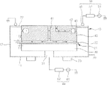
图1是概念上展示根据本发明的实施例的等离子蚀刻设备的截面图;1 is a cross-sectional view conceptually showing a plasma etching apparatus according to an embodiment of the present invention;
图2是根据实施例的等离子蚀刻设备的平面图;2 is a plan view of a plasma etching apparatus according to an embodiment;
图3到图5是概念上展示根据实施例的等离子蚀刻设备的修改版本的截面图;且3 to 5 are cross-sectional views conceptually showing modified versions of the plasma etching apparatus according to the embodiment; and
图6是图5的等离子蚀刻设备中屏蔽的后视图。FIG. 6 is a rear view of a shield in the plasma etching apparatus of FIG. 5. FIG.
具体实施方式 Detailed ways
下文中,将参看附图详细描述本发明的优选实施例。然而,本发明不限于所述实施例,而是可实施成不同的形式。这些实施例仅用于说明的目的,且用于使所属领域的技术人员完全理解本发明的范围。附图中,相似参考标号表示相似元件。Hereinafter, preferred embodiments of the present invention will be described in detail with reference to the accompanying drawings. However, the present invention is not limited to the embodiments, but may be implemented in various forms. These examples are for illustrative purposes only, and are used to fully understand the scope of the present invention to those skilled in the art. In the drawings, like reference numerals indicate like elements.
图1是概念上展示根据本发明的实施例的等离子蚀刻设备的截面图。图2是根据实施例的等离子蚀刻设备的平面图。FIG. 1 is a cross-sectional view conceptually showing a plasma etching apparatus according to an embodiment of the present invention. FIG. 2 is a plan view of a plasma etching apparatus according to an embodiment.
参看图1和图2,此实施例的等离子蚀刻设备包括腔室10、安放有衬底20的衬底支撑件30、用于防止在除了衬底20的边缘部分21以外的衬底20的顶部表面的区域中产生等离子的屏蔽40、用于在衬底20的边缘部分21处产生等离子的等离子产生单元50,和用于将偏压施加到衬底支撑件30的偏压施加单元60。Referring to FIGS. 1 and 2, the plasma etching apparatus of this embodiment includes a
此实施例的等离子蚀刻设备进一步包括用于排出可能在蚀刻工艺期间产生的气体和反应副产物(例如,微粒)的排出单元70。The plasma etching apparatus of this embodiment further includes an
另外,衬底入口/出口(未图示)形成在腔室的一侧。驱动单元31进一步提供在衬底支撑件30下方,从而提升或降低衬底支撑件30以便帮助装载或卸载衬底。附加的提升销(lift pin)可安装在衬底支撑件30内部。也就是说,在通过驱动单元31降低衬底支撑件30之后,穿过衬底入口/出口来装载衬底20。随后,再次提升衬底支撑件30,且接着将已装载的衬底20安放在衬底支撑件30上,藉此帮助装载衬底20。此外,可通过驱动单元31的提升操作来调节衬底20与屏蔽40之间的间隔。衬底支撑件30形成为呈圆环板的形状,其直径小于衬底20的直径。衬底20的底部的中心部分紧密接触衬底支撑件30。因此,衬底20的底部的边缘部分21由于衬底支撑件30的尺寸而暴露。衬底支撑件30具有与屏蔽40相同的直径,且因此边缘部分21同样暴露在衬底20的顶部和底部处。也就是说,由于衬底支撑件30的尺寸而暴露的边缘部分21的顶侧区域和底侧区域(图1中的T1)优选地具有距衬底20的外周边1到4毫米的宽度。因此,用于产生等离子的空间被提供在衬底20的边缘部分21与腔室10的内侧壁12之间。优选地,衬底支撑件30由导电材料形成,从而衬底支撑件30可接收外部偏压并将偏压电力施加到衬底20。尽管上文中衬底支撑件30和屏蔽40形成为具有相同直径,但其不限于此。例如,可形成衬底支撑件30使得其直径小于屏蔽40的直径。In addition, a substrate inlet/outlet (not shown) is formed on one side of the chamber. A driving
屏蔽40形成为呈圆环板或圆柱的形状,其直径小于衬底20的直径。屏蔽40经配置以屏蔽衬底20的顶部表面的中心部分处的将形成有图案的区域,并暴露衬底20的边缘部分21的顶侧区域。也就是说,使用不在等离子放电中恒定间隙内产生等离子的原则来配置屏蔽40,使得衬底20与屏蔽40之间的间隔是除了衬底20的边缘部分21的顶侧区域以外的区域中的恒定间隙。在衬底20的边缘部分21的顶侧区域与腔室10的内侧壁12之间提供用于产生等离子的空间。The
此处,衬底20的边缘部分的顶侧区域(图1中的T2)表示不形成用于构造装置的图案的区域,且具有从衬底20的外周边向内1到4毫米范围内的宽度。衬底20的边缘部分可以具有一确定的校准键。此处,优选地,衬底20与屏蔽40之间的间隔(图1的T3)在0.1到3毫米范围内。在衬底20与屏蔽40之间的间隔小于此范围的情况下,衬底20的顶部表面上的图案可能被破坏。在间隔大于此范围的情况下,等离子可能穿透到衬底20与屏蔽40之间的空间中,或可能产生在衬底20与屏蔽40之间的空间中。Here, the topside region (T2 in FIG. 1 ) of the edge portion of the
如图1所示,屏蔽40可与腔室10的顶壁13形成为整体或与腔室10的顶壁13分离。在屏蔽40与顶壁13分离的情况下,屏蔽40可垂直地移动,从而可容易地装载和卸载衬底20,且可便利地调节衬底20与屏蔽40之间的间隔。As shown in FIG. 1 , the
另外,可在屏蔽40内部形成复数个通道,从而可将外部气体供应到腔室10中。也就是说,如图1所示,用于在屏蔽40与衬底20之间喷射气帘气体的气帘气体通道41包含在屏蔽40中。通过穿过气帘气体通道将气帘气体喷射到屏蔽40与衬底20之间的空间中,可防止将形成在屏蔽40旁(即,在衬底20的边缘部分21处)的等离子引入到屏蔽40与衬底20之间的空间中。此外,屏蔽包含反应气体供应通道42和用于将反应气体供应到屏蔽40的一侧(即,供应到屏蔽40与腔室10的内侧壁12之间的区域)的气体注射喷嘴43。此时,反应气体的实例包含Ar、CF4、SF6、Cl2和类似物。可沿着圆环屏蔽40的圆周形成复数个气体注射喷嘴43。In addition, a plurality of passages may be formed inside the
如上所述,衬底20的边缘部分21暴露于由腔室10的内侧壁12与屏蔽40和衬底支撑件30的侧表面界定的空间。在衬底20的暴露的边缘部分21与腔室10的顶壁13、内侧壁12和底壁11之间维持足以产生等离子的空间。As described above, the
通过前述等离子产生单元50在衬底20的暴露的边缘部分21处产生等离子,藉此蚀刻衬底20的暴露的边缘部分。Plasma is generated at the exposed
为此,等离子产生单元50利用使用电感耦合的等离子(ICP)的设备。因此,等离子产生单元50包括用于产生高频电力的高频电力发生器51、用于高频电力的阻抗匹配的阻抗匹配装置52,和用于接收阻抗匹配的高频电力的天线53。For this, the
如图2所示,天线53形成在腔室10的内侧壁12与屏蔽40之间在腔室的顶壁13上呈圆环带的形状。天线53为在衬底20的暴露的边缘部分21处产生等离子供应电力。此时,天线53可形成为螺旋形状。与背景技术部分中已描述的电容耦合等离子的情况相比,在使用电感耦合的等离子的情况下,可在相对较宽的空间中产生具有高密度的等离子。因此,当离子与晶片碰撞时可改进离子的直线性,藉此改进蚀刻轮廓和蚀刻速率。As shown in FIG. 2 , the
优选地,安置有天线53的腔室10的顶壁13上的区域由绝缘材料22形成。因此,通过天线53向腔室10的内部施加高频电力而不产生损失,藉此在衬底20的边缘部分处产生等离子。另外,除了腔室10的顶壁13以外的腔室10的侧壁接地。Preferably, the area on the top wall 13 of the
将了解,绝缘材料22可能不与顶壁13形成为整体,而是可能仅插入到安置有天线53的顶壁13上的区域中。另外,如附图所示,可在顶壁13下面形成附加的绝缘材料22。此处,绝缘材料可包含陶瓷材料,但不限于此。It will be appreciated that the insulating
偏压施加单元60包括用于产生偏压电力的偏压电力发生器61,和用于匹配偏压电力的阻抗并将其传输到衬底支撑件30的阻抗匹配装置62。偏压施加单元60通过衬底支撑件30将阻抗匹配的偏压电力传输到衬底20,从而通过偏压加速等离子的离子能量以便使用等离子来改进蚀刻速率。The
下文将简要解释前述等离子蚀刻设备的操作。The operation of the aforementioned plasma etching apparatus will be briefly explained below.
将衬底20装载在放置在腔室10内部的衬底支撑件30上。调节屏蔽40与衬底20之间的距离达到不产生等离子的程度。随后,在将腔室10的内部压力维持在50毫托到2托的同时,通过屏蔽40供应反应气体和气帘气体。通过安置在腔室10的顶壁13上的天线53将阻抗匹配的等离子产生电力供应到腔室10中。因此,在衬底20的边缘部分21处(即,在腔室10的内侧壁12与屏蔽40和衬底支撑件30的侧表面之间)产生等离子。当从偏压施加单元60通过衬底支撑件30向衬底20施加偏压时,离子被加速,且加速的离子与衬底20的边缘部分21碰撞以执行蚀刻。蚀刻之后,通过安置在衬底支撑件30下方的排出单元70容易地排出所产生的微粒。此时,由于继续将气帘气体喷射到屏蔽40与衬底20之间的空间中,所以等离子不扩散到屏蔽40与衬底20之间的空间中。气帘气体的实例包含N2或其它惰性气体。The
在此实施例中,可使用附加的注射装置而不通过屏蔽40将反应气体供应到腔室10中。优选地,反应气体供应构件经构造以通过腔室的外壁供应反应气体。还将了解,反应气体供应构件(未图示)可安置在安装在腔室10的顶壁13上的绝缘材料22中。因此,由于反应气体供应构件安置在用来施加等离子产生电力的天线下方,所以可容易地产生等离子。In this embodiment, an additional injection device may be used to supply the reactive gas into the
另外,用于为等离子的产生供应电力的天线的配置、用于喷射气帘气体的流动通道的配置,和供应电力的方法可以各种方式实现,下文将参看附图对此进行描述。In addition, the configuration of the antenna for supplying power for generation of plasma, the configuration of the flow channel for ejecting the curtain gas, and the method of supplying power can be implemented in various ways, which will be described below with reference to the drawings.
图3到图5是是概念上展示根据本发明的实施例的等离子蚀刻设备的修改版本的截面图。图6是图5的等离子蚀刻设备中屏蔽的后视图。3 to 5 are cross-sectional views conceptually showing a modified version of the plasma etching apparatus according to the embodiment of the present invention. FIG. 6 is a rear view of a shield in the plasma etching apparatus of FIG. 5. FIG.
参看图3,天线53可配置成螺旋形状以缠绕在腔室10的外侧壁12周围。将等离子产生电力施加到安置在腔室10的外侧壁12上的天线53以便在腔室10内部产生等离子。此时,优选地,将绝缘材料22安装在腔室10的外侧壁12上。如附图中所示,可以一方式安装天线53使得单一的天线缠绕在腔室10的外侧壁12周围若干圈。或者,可配置一个或一个以上天线(每一天线形成为呈圆环条带的形状以便缠绕腔室10一圈),同时其彼此串联或并联连接。除了侧壁12以外的腔室10的其它部分接地。Referring to FIG. 3 , the
另外,参看图4,天线53可形成为呈圆环条带的形状,安装在腔室10的底壁11上。此时,天线53可形成为螺旋形状。等离子产生电源51将电力供应到安置在腔室10的底壁11上的天线53以便在腔室10内部产生等离子。此时,将绝缘材料22安装在腔室10的底壁11上。In addition, referring to FIG. 4 , the
此外,在天线53安置在腔室10的底壁11上的情况下,可通过腔室10的底壁11来供应反应气体。可将排出单元70安置在腔室10的顶壁上的区域处以便通过腔室10的顶壁排出微粒。In addition, in a case where the
另外,如图5和图6所示,气帘气体通道41形成在屏蔽40中以便将气帘气体喷射到屏蔽40与衬底20之间的空间中。如图6所示,气帘气体通道41包括形成在屏蔽40的中心处的第一气帘气体通道41a、形成在屏蔽40的边缘处的第二气帘气体通道41c,和形成在第一与第二气帘气体通道41a与41c之间的第三气帘气体通道41b。此处,第二与第三气帘气体通道41b与41c的喷射口形成为呈圆环条带的形状,使得可将气帘气体喷射在衬底20的整个中心部分上方。因此,可防止在衬底20的边缘部分21处产生的等离子扩散到衬底20的中心部分中。气帘气体通道41不限于上述气帘气体通道,而是可以各种方式形成,只要可防止等离子扩散到衬底的中心部分中。除了气帘气体通道以外,反应气体供应通道42和气体注射喷嘴43也可包括如上所述的复数个通道。In addition, as shown in FIGS. 5 and 6 , a
另外,单一的电力发生器80将电力供应到天线53以便在衬底20的边缘部分21与腔室的内侧壁之间产生等离子,并同时将电力供应到衬底支撑件30以便向其施加偏压。也就是说,第一匹配电路81和第二匹配电路82连接到单一的电力发生器80。第一匹配电路81连接到天线53,且第二匹配电路82连接到衬底支撑件30。以此方式,将从共同电力发生器80产生的电力通过第一匹配电路81施加到天线53以便产生等离子,且同样通过第二匹配电路82施加到衬底支撑件30以便将偏压施加到衬底支撑件30。In addition, a
如上所述,根据本发明,屏蔽和衬底支撑件防止在除了衬底的边缘部分以外的衬底的其它部分处产生等离子。使用电感耦合的等离子的放电来产生具有高密度的等离子,藉此去除残留在衬底的边缘部分处的薄膜和微粒。As described above, according to the present invention, the shield and the substrate support prevent plasma from being generated at portions of the substrate other than the edge portion of the substrate. The discharge of inductively coupled plasma is used to generate plasma with a high density, thereby removing thin films and particles remaining at the edge portion of the substrate.
另外,通过对电感耦合的等离子进行放电,可能改进衬底的边缘部分处的蚀刻速率并在低处理压力下适当地调节已蚀刻的轮廓。In addition, by discharging the inductively coupled plasma, it is possible to improve the etching rate at the edge portion of the substrate and properly adjust the etched profile at low process pressure.
此外,通过屏蔽将气帘气体喷射到衬底的顶部表面的中心区域,从而防止将等离子引入到衬底与屏蔽之间的空间中。In addition, the curtain gas is sprayed to the central region of the top surface of the substrate through the shield, thereby preventing the introduction of plasma into the space between the substrate and the shield.
Claims (8)
Applications Claiming Priority (3)
| Application Number | Priority Date | Filing Date | Title |
|---|---|---|---|
| KR10-2005-0069391 | 2005-07-29 | ||
| KR1020050069391A KR101149332B1 (en) | 2005-07-29 | 2005-07-29 | Etching apparatus using the plasma |
| KR1020050069391 | 2005-07-29 |
Publications (2)
| Publication Number | Publication Date |
|---|---|
| CN1905135A CN1905135A (en) | 2007-01-31 |
| CN1905135B true CN1905135B (en) | 2012-05-09 |
Family
ID=36954515
Family Applications (1)
| Application Number | Title | Priority Date | Filing Date |
|---|---|---|---|
| CN2006101039752A Active CN1905135B (en) | 2005-07-29 | 2006-07-28 | Plasma etching apparatus |
Country Status (6)
| Country | Link |
|---|---|
| US (2) | US7879187B2 (en) |
| EP (1) | EP1748465B1 (en) |
| JP (1) | JP4956080B2 (en) |
| KR (1) | KR101149332B1 (en) |
| CN (1) | CN1905135B (en) |
| TW (1) | TWI404138B (en) |
Families Citing this family (16)
| Publication number | Priority date | Publication date | Assignee | Title |
|---|---|---|---|---|
| KR100978754B1 (en) * | 2008-04-03 | 2010-08-30 | 주식회사 테스 | Plasma processing equipment |
| US8398778B2 (en) | 2007-01-26 | 2013-03-19 | Lam Research Corporation | Control of bevel etch film profile using plasma exclusion zone rings larger than the wafer diameter |
| WO2008114958A1 (en) | 2007-03-16 | 2008-09-25 | Sosul Co., Ltd. | Apparatus for plasma processing and method for plasma processing |
| US8980049B2 (en) | 2007-04-02 | 2015-03-17 | Charm Engineering Co., Ltd. | Apparatus for supporting substrate and plasma etching apparatus having the same |
| US7981307B2 (en) * | 2007-10-02 | 2011-07-19 | Lam Research Corporation | Method and apparatus for shaping gas profile near bevel edge |
| WO2013048013A1 (en) * | 2011-09-28 | 2013-04-04 | 한국기초과학지원연구원 | Non-contact type plasma ashing apparatus |
| KR101405066B1 (en) * | 2011-09-28 | 2014-06-13 | 한국기초과학지원연구원 | Non-contact plasma ashing apparatus |
| KR101415740B1 (en) * | 2012-10-04 | 2014-07-04 | 한국기초과학지원연구원 | Ashing apparatus using remote plasma source |
| KR20140140418A (en) * | 2013-05-29 | 2014-12-09 | 삼성디스플레이 주식회사 | Apparatus and Method for organic layer etching |
| EP3092324B1 (en) | 2014-01-09 | 2020-07-15 | United Technologies Corporation | Coating process using gas screen |
| US9885110B2 (en) | 2014-08-06 | 2018-02-06 | United Technologies Corporation | Pressure modulated coating |
| US11866816B2 (en) | 2016-07-06 | 2024-01-09 | Rtx Corporation | Apparatus for use in coating process |
| US20190119815A1 (en) * | 2017-10-24 | 2019-04-25 | Applied Materials, Inc. | Systems and processes for plasma filtering |
| KR20260049677A (en) * | 2019-04-11 | 2026-04-14 | 어플라이드 머티어리얼스, 인코포레이티드 | Plasma densification within a processing chamber |
| US10749248B1 (en) * | 2019-09-23 | 2020-08-18 | Qualcomm Incorporated | Antenna module placement and housing for reduced power density exposure |
| CN119495544A (en) * | 2023-08-21 | 2025-02-21 | 中微半导体设备(上海)股份有限公司 | Etching device, substrate processing system and device preparation method thereof |
Citations (1)
| Publication number | Priority date | Publication date | Assignee | Title |
|---|---|---|---|---|
| CN1481207A (en) * | 2002-09-04 | 2004-03-10 | ���ǵ�����ʽ���� | Inductively coupled plasma generator combined with double-layer coil antenna |
Family Cites Families (20)
| Publication number | Priority date | Publication date | Assignee | Title |
|---|---|---|---|---|
| US5384008A (en) * | 1993-06-18 | 1995-01-24 | Applied Materials, Inc. | Process and apparatus for full wafer deposition |
| JP3521587B2 (en) * | 1995-02-07 | 2004-04-19 | セイコーエプソン株式会社 | Method and apparatus for removing unnecessary substances from the periphery of substrate and coating method using the same |
| US5710486A (en) * | 1995-05-08 | 1998-01-20 | Applied Materials, Inc. | Inductively and multi-capacitively coupled plasma reactor |
| DE19622015A1 (en) * | 1996-05-31 | 1997-12-04 | Siemens Ag | Process for etching destruction zones on a semiconductor substrate edge and etching system |
| EP0840350A2 (en) | 1996-11-04 | 1998-05-06 | Applied Materials, Inc. | Plasma apparatus and process with filtering of plasma sheath-generated harmonics |
| US6149730A (en) * | 1997-10-08 | 2000-11-21 | Nec Corporation | Apparatus for forming films of a semiconductor device, a method of manufacturing a semiconductor device, and a method of forming thin films of a semiconductor |
| US6271129B1 (en) | 1997-12-03 | 2001-08-07 | Applied Materials, Inc. | Method for forming a gap filling refractory metal layer having reduced stress |
| US6335293B1 (en) | 1998-07-13 | 2002-01-01 | Mattson Technology, Inc. | Systems and methods for two-sided etch of a semiconductor substrate |
| US6492612B1 (en) * | 1998-12-28 | 2002-12-10 | Tokyo Electron Limited | Plasma apparatus and lower electrode thereof |
| US6261406B1 (en) * | 1999-01-11 | 2001-07-17 | Lsi Logic Corporation | Confinement device for use in dry etching of substrate surface and method of dry etching a wafer surface |
| US20020142612A1 (en) * | 2001-03-30 | 2002-10-03 | Han-Ming Wu | Shielding plate in plasma for uniformity improvement |
| KR100433008B1 (en) | 2001-04-18 | 2004-05-31 | (주)소슬 | plasma etching device |
| KR100428813B1 (en) * | 2001-09-18 | 2004-04-29 | 주성엔지니어링(주) | Plama generation apparatus and SiO2 thin film etching method using the same |
| DE10340147B4 (en) * | 2002-08-27 | 2014-04-10 | Kyocera Corp. | Dry etching and dry etching |
| JP3692133B2 (en) * | 2002-12-04 | 2005-09-07 | 積水化学工業株式会社 | Normal pressure plasma processing apparatus for wafer outer edge and processing method such as etching |
| JP3712125B2 (en) * | 2003-02-03 | 2005-11-02 | 東京応化工業株式会社 | Plasma processing equipment |
| JP4394073B2 (en) * | 2003-05-02 | 2010-01-06 | 東京エレクトロン株式会社 | Process gas introduction mechanism and plasma processing apparatus |
| US7615131B2 (en) * | 2003-05-12 | 2009-11-10 | Sosul Co., Ltd. | Plasma etching chamber and plasma etching system using same |
| US20060000802A1 (en) * | 2004-06-30 | 2006-01-05 | Ajay Kumar | Method and apparatus for photomask plasma etching |
| US7943007B2 (en) * | 2007-01-26 | 2011-05-17 | Lam Research Corporation | Configurable bevel etcher |
-
2005
- 2005-07-29 KR KR1020050069391A patent/KR101149332B1/en not_active Expired - Fee Related
-
2006
- 2006-07-26 JP JP2006203029A patent/JP4956080B2/en active Active
- 2006-07-27 US US11/460,557 patent/US7879187B2/en not_active Expired - Fee Related
- 2006-07-28 EP EP06118053.5A patent/EP1748465B1/en not_active Ceased
- 2006-07-28 TW TW095127843A patent/TWI404138B/en active
- 2006-07-28 CN CN2006101039752A patent/CN1905135B/en active Active
-
2010
- 2010-12-13 US US12/967,026 patent/US8177992B2/en active Active
Patent Citations (1)
| Publication number | Priority date | Publication date | Assignee | Title |
|---|---|---|---|---|
| CN1481207A (en) * | 2002-09-04 | 2004-03-10 | ���ǵ�����ʽ���� | Inductively coupled plasma generator combined with double-layer coil antenna |
Also Published As
| Publication number | Publication date |
|---|---|
| KR20070014601A (en) | 2007-02-01 |
| EP1748465B1 (en) | 2015-04-15 |
| KR101149332B1 (en) | 2012-05-23 |
| TWI404138B (en) | 2013-08-01 |
| JP2007043148A (en) | 2007-02-15 |
| TW200721299A (en) | 2007-06-01 |
| CN1905135A (en) | 2007-01-31 |
| KR101149332B9 (en) | 2025-01-10 |
| US7879187B2 (en) | 2011-02-01 |
| US8177992B2 (en) | 2012-05-15 |
| EP1748465A3 (en) | 2009-10-14 |
| US20110079581A1 (en) | 2011-04-07 |
| JP4956080B2 (en) | 2012-06-20 |
| US20070029044A1 (en) | 2007-02-08 |
| EP1748465A2 (en) | 2007-01-31 |
Similar Documents
| Publication | Publication Date | Title |
|---|---|---|
| US8177992B2 (en) | Plasma etching apparatus | |
| JP5179730B2 (en) | Plasma etching equipment | |
| TWI404165B (en) | Substrate supporting device and plasma etching device comprising the same | |
| US8261691B2 (en) | Plasma processing apparatus | |
| KR101124938B1 (en) | Plasma processing apparatus | |
| CN102473634B (en) | Plasma processing device and plasma processing method | |
| US10418224B2 (en) | Plasma etching method | |
| JP2007043149A5 (en) | ||
| TWI502619B (en) | Electrode for plasma processing apparatus, plasma processing apparatus, and method for generating plasma using plasma processing apparatus | |
| US20110263130A1 (en) | Methods for rf pulsing of a narrow gap capacitively coupled reactor | |
| KR101411171B1 (en) | Plasma processing apparatus | |
| KR101423554B1 (en) | Plasma etching apparatus and wafer etching method using the same | |
| KR101146132B1 (en) | Plasma processing apparatus | |
| KR20070058760A (en) | Low Pressure Plasma Generator | |
| KR100725614B1 (en) | Plasma processing apparatus | |
| KR20080020722A (en) | Plasma processing apparatus and substrate processing method using the same | |
| JP2016134460A (en) | Plasma processing device and plasma processing method |
Legal Events
| Date | Code | Title | Description |
|---|---|---|---|
| C06 | Publication | ||
| PB01 | Publication | ||
| C10 | Entry into substantive examination | ||
| SE01 | Entry into force of request for substantive examination | ||
| C14 | Grant of patent or utility model | ||
| GR01 | Patent grant |