CN1893105A - Light emitting device, method of manufacturing the same, and electronic apparatus - Google Patents
Light emitting device, method of manufacturing the same, and electronic apparatus Download PDFInfo
- Publication number
- CN1893105A CN1893105A CN 200610088799 CN200610088799A CN1893105A CN 1893105 A CN1893105 A CN 1893105A CN 200610088799 CN200610088799 CN 200610088799 CN 200610088799 A CN200610088799 A CN 200610088799A CN 1893105 A CN1893105 A CN 1893105A
- Authority
- CN
- China
- Prior art keywords
- electrode
- organic
- substrate
- layer
- film
- Prior art date
- Legal status (The legal status is an assumption and is not a legal conclusion. Google has not performed a legal analysis and makes no representation as to the accuracy of the status listed.)
- Pending
Links
Images


Landscapes
- Electroluminescent Light Sources (AREA)
Abstract
To provide an organic EL device having a structure where a plurality of light emitting elements are connected in series to one another and manufactured by using an ink jet method; and to provide its manufacturing method. This organic EL device is provided with: a first substrate S1 with a plurality of organic EL elements 61, 62 and 63 formed in each of a plurality of pixels; and a second substrate on which driving TFTs 123 are formed corresponding to the pixels and connected to the first substrate S1 through a conductive connection member 30. Electrodes 23a, 23b and 23c provided for the organic EL elements 61, 62 and 63, respectively, are separated by a reversely tapered resist layer 48; a transparent electrode 50a of each organic EL element 61 is electrically connected to the electrode 23b of the organic EL element 62; and a transparent electrode 50b of each organic EL element 62 is electrically connected to the electrode 23c of the organic EL element 63. Thereby, the organic EL elements 61, 62 and 63 formed in an each pixel are connected in series to one another.
Description
Technical field
The present invention relates to light-emitting device, its manufacture method and the electronic equipment of organic El device etc.
Background technology
As the self-emission device that does not need grade backlight, the organic El device that possesses organic electroluminescent (below be called organic EL) element is in recent years gazed at.Organic EL is that to possess organic EL layer between relative pair of electrodes be the element that light-emitting component constitutes, and carries out the colored organic El device that shows and possesses the light-emitting component that has with red (R), green (G), blueness (B) corresponding emission wavelength frequency band of all kinds.After applying voltage between relative pair of electrodes, injected electrons and hole be combination again in luminescent film, makes this luminescent film luminous thus.The luminescent film that forms in such organic El device uses the film less than 1 μ m degree to form usually.In addition, organic El device because luminescent film self is luminous, thus need in existing liquid crystal indicator, not use especially backlight.Therefore, organic El device have can thickness do so as thin as a wafer advantage.
But, for organic El device, it is maximized, but the distribution length of power line etc. increase along with the maximization of organic El device, voltage descends and becomes remarkable.Therefore, organic El device maximizes, near the then remarkable more reduction of the brightness the central authorities of luminous zone.As solution to this problem, in the patent documentation 1 below, proposed in a pixel, to be provided with the suggestion of the parts of the adjacent a plurality of light-emitting components of series connection.Be located on the light-emitting component and apply voltage V[V] time flow through electric current I [A] in this light-emitting component, can obtain L[cd/m
2] luminosity.Now, getting in the structure of the individual this light-emitting component of series connection n (n is the integer more than 2 or 2) and applying voltage is nV[V] time, for the average luminescence brightness that makes each light-emitting component is L[cd/m
2], can make in each light-emitting component and flow through I/n[A] electric current.Because can be electric current from I[A for obtaining identical luminosity] be reduced to I/n[A], so the voltage drop Δ V that is caused by wiring resistance R also becomes 1/n, its result can suppress near the reduction of the brightness the central authorities of luminous zone.
As the method for the organic El device of making above structure, as disclosed in the following patent documentation 2, enumerated the method that negative electrode formation is carried out in the formation of using mask to carry out the formation of luminescent film of organic EL and the luminescent film that continues.In addition, as disclosed in the following patent documentation 3, enumerated and formed next door, formed the luminescent film of organic EL and the method for negative electrode by evaporation with contrary cone-shaped.
[patent documentation 1] spy opens the 2000-89691 communique
[patent documentation 2] spy opens the 2004-71570 communique
[patent documentation 3] spy opens the 2002-313572 communique
Summary of the invention
But, in recent years, watching attentively use ink-jet method on substrate, be coated with the formation material of the luminescent film that comprises organic EL aqueous body, make the method for this liquid dryer formation luminescent film.This ink-jet method is expected to not only in the formation of the luminescent film of organic EL, and also is used when forming various fine structure.By using this ink-jet method, with comparison under the situation of using mask formation fine structure, because do not need the mask of high price sometimes, so have the advantage of the cost degradation that can realize organic El device.In addition, form fine structure because can only only spray necessary material, so can realize the saving of resource in the position of necessity.
Organic El device with disclosed structure in the above-mentioned patent documentation 1, can use disclosed technology manufacturing in the above-mentioned patent documentation 2,3, can not be but exist only by one of manufacturing process (for example forming process of the luminescent film of organic EL) simple substitute is brought into play the such problem of organic El device of expectation function for the ink-jet method manufacturing.
One of effect of the present invention that describes in detail below is used to address the above problem.
Light-emitting device of the present invention, comprise a plurality of first electrodes, a plurality of second electrode, a plurality of luminescent film, it is characterized in that, each of described a plurality of luminescent film is configured between one first electrode and one second electrode in a plurality of second electrode in described a plurality of first electrode, and described one first electrode is electrically connected with second electrode adjacent to described one second electrode in described a plurality of second electrodes.
In above-mentioned light-emitting device, also can pass through insulating element described a plurality of first electrodes disconnected from each other, by insulating element described a plurality of second electrodes disconnected from each other, by insulating element described a plurality of luminescent film disconnected from each other.
In above-mentioned light-emitting device, also can separate described a plurality of second electrodes by first insulating element with first cone-shaped.
In above-mentioned light-emitting device, second insulating element that joins, has the cone-shaped opposite with described first cone-shaped with described first insulating element can be set also.
Above-mentioned light-emitting device can use in the display part of electronic equipment etc.
The manufacture method of light-emitting device of the present invention is characterised in that, comprise: first operation that forms a plurality of first electrodes on first substrate, form second operation of first insulating element of described a plurality of first electrodes disconnected from each other, on described first insulating element, form the 3rd operation of second insulating element with the opposite cone-shaped of the cone-shaped that has with described first insulating element, on described a plurality of first electrodes, spray the aqueous body of the formation material that comprises luminescent film by drop ejection method, above each of described a plurality of first electrodes, form the 4th operation of luminescent film, with formation material by evaporation second electrode, in disconnected from each other, form the 5th operation of second electrode that is connected with one first electrode at least in described a plurality of first electrode by described second insulating element.
For addressing the above problem, organic El device of the present invention is the organic El device with a plurality of pixels, it is characterized in that having: a plurality of first electrodes that separate by the next door in described pixel; The a plurality of illuminating parts that form by drop ejection method on each top of described a plurality of first electrodes; A plurality of second electrodes that separating component that form on each top of described a plurality of illuminating parts, by contrary cone-shaped separates have first substrate of a plurality of light-emitting components that connect adjacent described first electrode and described second electrode and connect in described pixel; Second substrate of luminous a plurality of driving elements with having corresponding described light-emitting component that be provided with, that corresponding described pixel is had with each of described pixel.
According to the present invention, because have each a plurality of light-emitting components of a plurality of pixels of series connection, so can be reduced to the electric current that flows through each light-emitting component the part of the light-emitting component that in pixel, is provided with, its result can suppress near the brightness reduction the viewing area central authorities that cause because voltage descends.In addition, because can reduce electric current,, can realize that consequently height becomes more meticulous so the distribution of supply power can be run business into particular one.
In addition, organic El device of the present invention is characterised in that each of described a plurality of pixels has 2 to 4 described light-emitting components.
Because along with the number increase of the light-emitting component of each pixel setting can reduce electric current, so the viewpoint that reduces from brightness it seems that how better the number of the light-emitting component that is provided with the pixel is.But, the number of the light-emitting component of each pixel setting increases, causes that aperture opening ratio reduces along with increasing the next door number.Therefore, consider the viewpoint both sides that viewpoint that brightness reduces and aperture opening ratio reduce, the number of wishing the light-emitting component in the pixel for more than or equal to two smaller or equal to four.
In addition, organic El device of the present invention is characterised in that described illuminating part comprises hole transmission layer and luminescent film forms.
According to the present invention,,, also can improve injection rate by hole transmission layer so supposition worsens to the hole of the luminescent film that forms by drop ejection method injection rate because illuminating part comprises hole transmission layer and luminescent film forms.
In addition, organic El device of the present invention wishes that the described second substrate dual-purpose seals the hermetic sealing substrate of described first substrate.
In addition, organic El device of the present invention, the described driving element that hope is provided with on described second substrate in the light-emitting component that is provided with in the described pixel of correspondence, is connected by described second electrode of conductive connecting member with the light-emitting component of the end that is positioned at described pixel.
In addition, organic El device of the present invention is characterised in that, described driving element is the part of a plurality of elements that form on the substrate of regulation is transferred on described second substrate selectively and is set at element on described second substrate.
For addressing the above problem, the manufacture method of organic El device of the present invention is the manufacture method with organic El device of a plurality of pixels, it is characterized in that, has: first operation that forms a plurality of first electrodes in the described pixel on first substrate; At least between described first electrode, form second operation in the next door of separating described first electrode in the described pixel; On described next door, form the 3rd operation of the separating component of contrary cone-shaped; On described first electrode, spray the aqueous body of the formation material that comprises luminescent film by drop ejection method, and form the 4th operation of luminescent film on each top of described first electrode; The formation material of evaporation second electrode on described first substrate by the time disconnected from each other, forms the 5th operation that is connected with second electrode of described first electrode that forms on the position adjacent by described separating component; The second substrate corresponding setting with each of described pixel of configuration, that have the luminous a plurality of driving elements of described light-emitting component that corresponding described pixel is had makes the 6th operation with the described light-emitting component electrical connection of each corresponding described pixel of described driving element.
According to the present invention, because in each pixel of a plurality of pixels, form a plurality of light-emitting components of series connection, so can be reduced to the electric current that flows through each light-emitting component the part of the light-emitting component that in pixel, is provided with, its result can suppress near the reduction of the brightness the viewing area central authorities that cause because voltage descends.In addition, because can reduce electric current,, can realize that consequently height becomes more meticulous so the distribution of supply power can be run business into particular one.Have again,,, can save resource so can not waste the formation material that uses luminescent film because form luminescent film by drop ejection method.
In addition, the manufacture method of organic El device of the present invention is characterised in that, in each pixel of a plurality of pixels, to form described light-emitting component in 2 to 4 the scope.
Because along with the number increase of the light-emitting component of each pixel setting can reduce electric current, so how better the number of the light-emitting component that is provided with from the viewpoint pixel that brightness reduces is.But, the number of the light-emitting component of each pixel setting increases, causes that aperture opening ratio reduces along with increasing the next door number.Therefore, consider the viewpoint both sides that viewpoint that brightness reduces and aperture opening ratio reduce, preferred, the number of the light-emitting component in the pixel for more than or equal to 2 smaller or equal to 4.
In addition, the manufacture method of organic El device of the present invention is characterised in that, is included in the top of described luminescent film or the 6th operation that hole transmission layer is formed at the bottom.
According to the present invention,,, also can improve injection rate by hole transmission layer so supposition worsens to the hole of the luminescent film that forms by drop ejection method injection rate because form hole transmission layer in the top or the bottom of luminescent film.
In addition, the manufacture method of organic El device of the present invention, described the 6th operation is preferred: dispose described second substrate for described first substrate, make the described second substrate dual-purpose seal the hermetic sealing substrate of described first substrate.
In addition, the manufacture method of organic El device of the present invention, wish that described the 6th operation is preferred: fall the described driving element that on described second substrate, is provided with, in the light-emitting component that in the described pixel of correspondence, is provided with, be connected by described second electrode of conductive connecting member with the light-emitting component of the end that is positioned at described pixel.
Perhaps, the manufacture method of organic El device of the present invention is characterised in that, be included in and form the 8th operation of a plurality of described driving elements on the substrate of regulation and fall that a part at the described a plurality of driving elements that form on the substrate of described regulation is transferred on described second substrate selectively and described driving element is arranged on the 9th operation on described second substrate.
Electronic equipment of the present invention is characterised in that to have above-mentioned any one described organic El device or have the organic El device of making by the manufacture method of above-mentioned any one described organic El device.
According to such structure, can provide electronic equipment with good display characteristic.
Description of drawings
Fig. 1 is the ideograph of expression according to the distribution structure of the organic El device of an embodiment of the invention.
Fig. 2 is the plane graph of pattern ground expression according to the structure of the organic El device 1 of an embodiment of the invention.
Fig. 3 is the plane perspective view according to the organic El device 1 of an embodiment of the invention.
Fig. 4 amplifies the plane perspective view of expression according to the pixel region X of an embodiment of the invention.
Fig. 5 is the sectional view along the A-B line among Fig. 4.
Fig. 6 is the process chart of expression formation according to an example of the manufacturing process of the second substrate S2 of the part of the organic El device of an embodiment of the invention.
Fig. 7 is the process chart of expression formation according to an example of the manufacturing process of the second substrate S2 of the part of the organic El device of an embodiment of the invention.
Fig. 8 is the process chart of expression formation according to an example of the manufacturing process of the first substrate S1 of the part of the organic El device of an embodiment of the invention.
Fig. 9 is the process chart of expression formation according to an example of the manufacturing process of the first substrate S1 of the part of the organic El device of an embodiment of the invention.
Figure 10 amplifies the plane perspective view of expression according to the pixel region X of another embodiment of the present invention.
Figure 11 is the sectional view along the A-B line among Figure 10.
Figure 12 is the process chart of expression according to an example of the manufacture method of the organic El device of another embodiment of the present invention.
Figure 13 is the process chart of expression according to an example of the manufacture method of the organic El device of another embodiment of the present invention.
Figure 14 is the process chart of expression according to an example of the manufacture method of the organic El device of another embodiment of the present invention.
Figure 15 is the figure of the example of expression electronic equipment of the present invention.
Among the figure:
The 1-organic El device
23a, 23b, 23c-electrode (the 2nd electrode)
25-lyophily key-course (next door)
The 30-conductive connecting member
50-common electrode (the 1st electrode)
50a, 50b-transparency electrode (first electrode)
61,62,63-organic EL (light-emitting component)
70a, 70b, 70c-luminescent film (illuminating part)
123-drives with TFT (driving element)
The organic cofferdam layer of 221-(next door)
S1-first substrate
S2-second substrate
X-pixel region (pixel)
Embodiment
Describe organic El device, its manufacture method and electronic equipment with reference to the accompanying drawings in detail according to an embodiment of the invention.In addition, following Shuo Ming execution mode is represented not limit the mode of a part of the present invention the present invention, and can change arbitrarily in the scope of technological thought of the present invention.In addition, in each figure shown below, because get the size that to discern each layer or each parts degree in the drawings, so the engineer's scale difference of each layer or each parts.
[organic El device]
Fig. 1 is the ideograph of expression according to the distribution structure of the organic El device of an embodiment of the invention.Organic El device 1 shown in Figure 1, it is the device that uses the active matrix mode of thin-film transistor (TFT) as switch element, have by multi-strip scanning line 101, to many signal line 102 of extending with the direction of each scan line 101 quadrature and the distribution structure of forming with many power lines 103 of each holding wire 102 extension in parallel, near formation pixel region X each intersection point of scan line 101 and holding wire 102.
On holding wire 102, be connected with possess shift register, the data line drive circuit 100 of level shifter, video line and analog switch.In addition, on scan line 101, be connected with the scan line drive circuit 80 that possesses shift register and level shifter.
In each pixel region X, be provided with: the switch of supplying with sweep signal via scan line 101 to gate electrode with TFT112, keep the picture element signal supplied with from holding wire 102 with TFT112 via this switch maintenance electric capacity 113, to gate electrode supply with by the driving of the picture element signal that keeps electric capacity 113 to keep with TFT123, when being electrically connected with power line 103 with TFT123 via this drivings from the pixel electrode (electrode) 23 of power line 103 inflow drive currents and a plurality of organic ELs 61,62,63 that between this pixel electrode 23 and common electrode 50, dispose.
A plurality of organic ELs 61,62,63 series connection of configuration between pixel electrode 23 and common electrode 50, each all is independent luminous light-emitting component.Why adopting the structure that possesses a plurality of light-emitting components in each pixel region X, is because follow the distribution of maximization power line 103 of organic El device 1 elongated, for preventing because the cause that the luminosity of each pixel region X that the increase that voltage descends produces reduces.In addition, because can reduce to flow through the electric current of power line 103, so, can realize that also height becomes more meticulous by power line 103 is run business into particular one.
If the number of the organic EL that is provided with in pixel region X is n, then in the present embodiment, and compare under the situation that an organic EL is set in pixel region X, on power line 103, apply n voltage doubly.Thus, the electric current that can make the almost constant handle of luminosity of a pixel region X flow through power line 103 is taken as 1/n, and its result can prevent the reduction of the luminosity of each pixel region X of causing because voltage descends.
In addition, in the present embodiment, illustrate the structure that three organic ELs 61,62,63 are set in pixel region X, but can consider the performance of wishing etc. and the suitable number that is set in the organic EL that is provided with among the pixel region X.But the increase along with the number of the organic EL that is provided with in each pixel can cause the reduction of aperture opening ratio.Therefore, the both sides that consider the viewpoint of brightness reduction and the viewpoint that aperture opening ratio reduces wish that the number of the organic EL in the pixel is in 2 to 4 scope.
Fig. 2 is the plane graph of pattern ground expression according to the structure of the organic El device 1 of an embodiment of the invention.As shown in Figure 2, the organic El device 1 of present embodiment possesses: the pixel electrode that have the substrate 20 of the electrical insulating property of light transmission, is connected with switch with TFT (not shown) in the pixel electrode district (not shown) that forms with the matrix shape configuration on the substrate 20, the power line 103 that in configuration around the pixel electrode district, is connected, be arranged in overlooking in the pixel electrode district at least and see the pixel portions 3 that is roughly rectangle (single-point of figure rule frame) with each pixel electrode.In addition, the pixel portions 3 in the present embodiment, zoning are the real viewing area 4 (the double dot dash line frame among the figure in) of middle body and fabricate (dummy) district 5 (zones between single-point line and the double dot dash line) in configuration around the real viewing area 4.
In real viewing area 4, viewing area R, G, the B that has pixel electrode respectively in the drawings the H direction and the V direction on be configured regularly.In addition, each of these viewing areas R, G, B forms pixel region X shown in Figure 1.In addition, the both sides in Fig. 2 of real viewing area 4, configuration scan line drive circuit 8,80.This scan line drive circuit 8,80 is positioned at the lower layer side setting of fabricating district 5.In addition, the upper side configuration inspection circuit 90 in Fig. 2 of real viewing area 4, this check circuit 90 is provided with in the lower layer side configuration of fabricating district 5.This check circuit 90 is the circuit that are used to check the running-active status of organic El device 1, constitute: for example have inspection message output block (not shown), can carry out in making the way or the quality of the display unit when dispatching from the factory, the inspection of defective to outside outgoing inspection result.
The driving voltage of scan line drive circuit 80 and check circuit 90 applies via not shown voltage conductive part from the power supply unit of stipulating.In addition, to the drive control signal and the driving voltage of these scan line drive circuits 80 and check circuit 90, send and apply via not shown signal conduction portion from the master driver of the regulation of the action control of carrying out this organic El device 1 etc.In addition, the drive control signal under so-called this kind situation is the command signal of the related master driver of control from scan line drive circuit 80 and check circuit 90 output signals the time.
Fig. 3 is the plane perspective view according to the organic El device 1 of an embodiment of the invention.In addition, in Fig. 3, be the relation of clear and definite and Fig. 2, merge diagram pixel portions 3, real viewing area 4 and viewing area R, G, B.As shown in Figure 3, the face side at organic El device 1 is provided with transparent common electrode 50.This common electrode 50 for example by formation such as ITO, is gone up formation at the back side of the substrate 20 with light transmission (rear side of organic El device 1).
With real viewing area 4 corresponding central parts in, the H direction of common electrode 50 in figure extended, and forms a plurality of band shapes of arranging with the interval (arrangement pitch of viewing area) of regulation on the V direction in the drawings.Specifically, the organic El device 1 of present embodiment as shown in Figure 1, because a plurality of organic El devices of series connection are set, forms shape shown in Figure 3 to common electrode 50 in pixel region X.In addition, at the central portion of common electrode 50, forming transparency electrode 50a, the 50b (with reference to Fig. 5) that the part formation in addition of banded part is made up of the material identical with common electrode, but insulating with these transparency electrodes 50a, 50b.
Fig. 4 is the plane perspective view of amplifying remarked pixel district X.Among this external Fig. 4, amplify two adjacent pixel region X on the H direction that is illustrated among Fig. 2, omit switch shown in Figure 1 diagram with TFT112, maintenance electric capacity 113, driving TFT123, scan line 101, holding wire 102 and power line 103.As shown in Figure 4, in pixel region X, be formed with the organic EL 61,62,63 that Fig. 1 represents.
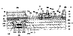
The electrode 23b of the transparency electrode 50a of organic EL 61 and organic EL 62 contacts and is electrically connected in the position of giving symbol P1.In addition, the electrode 23c of the transparency electrode 50b of organic EL 62 and organic EL 62 contacts and is electrically connected in the position of giving symbol P2.Like this, between electrode 23a that is equivalent to pixel electrode shown in Figure 1 23 and common electrode 50, be in series with organic EL 61,62,63.
Then, be described in more detail the cross section structure of pixel region X with reference to Fig. 5.Fig. 5 is the sectional view along the A-B line among Fig. 4.As shown in Figure 5, the organic El device 1 of present embodiment comprises: be formed with organic EL 61,62,63 the first substrate S1, be formed with make the luminous driving of these organic ELs 61,62,63 with the second substrate S2 of TFT123 etc., be electrically connected the conductive connecting member 30 of the first substrate S1 and the second substrate S2.As this conductive connecting member 30, for example can use silver-colored conductive paste.In addition, in the second substrate S2,, be formed with switch shown in Figure 1 and use TFT112 and keep electric capacity 113 except that driving with the TFT123, and scan line 101, holding wire 102 and power line 103.The structure of the second substrate S2 and the first substrate S1 is described below successively.
[second substrate]
The driving of the second substrate S2 forms on substrate 21 with TFT123 etc.As this substrate 21, can adopt transparent, translucent or opaque material.As transparent or translucent substrate, for example can enumerate glass, quartz, resin (plastics, plastic film) etc., especially preferably use glass substrate.In addition, the organic El device 1 of present embodiment, because be the light that sends that obtains from each pixel region X, launch the organic El device of (topemission) type from the so-called top that the opposition side with the second substrate S2 side that is formed with driving usefulness TFT123 takes out, so also can adopt opaque substrate.
On this substrate 21, be formed with to comprise and be used to drive the drive circuit portion of the driving of pixel electrode 23 (electrode 23a) with TFT123 etc.About the structure of this drive circuit portion, lifting driving is that example describes with TFT123.On the surface of substrate 21, be formed with SiO as substrate
2Substrate protective layer (omitting diagram) for main body is formed with silicon layer 241 on it.On the surface of this silicon layer 241, be formed with and comprise SiO
2And any at least gate insulator 282 among the SiN.
In addition, in above-mentioned silicon layer 241, clamping grid insulating barrier 282 and with gate electrode 242 overlapping areas as channel region 241a.In addition, this gate electrode 242 is parts of not shown scan line 101.On the other hand, covering silicon layer 241 and forming on the surface of gate insulator 282 of gate electrode 242, be formed with SiO
2First interlayer insulating film 283 for main body.
In addition, the source side at channel region 241a in silicon layer 241 is provided with source area 241S, on the other hand, in the drain side of channel region 241a drain region 241D is set.In addition, preferably when the source side of channel region 241a forms low concentration source area and high concentration source area, drain side at channel region 241a forms low concentration drain region and high concentration drain region, and makes so-called LDD (Lightly Doped Drain) structure.
Among these, source area 241S is connected with source electrode 243 via passing the contact hole 243a of gate insulator 282 with 283 perforates of first interlayer insulating film.This source electrode 243 constitutes as the part of above-mentioned power line 103 (with reference to Fig. 1, extend to the vertical direction of paper the position of the source electrode 243 in Fig. 5).On the other hand, drain region 241D is via the contact hole 244a that passes gate insulator 282 and 283 perforates of first interlayer insulating film, and by the drain electrode of forming with one deck with source electrode 243 244.
The upper strata that is formed with first interlayer insulating film 283 of source electrode 243 and drain electrode 244 is covered by for example second interlayer insulating film 284 based on the resinous principle of acrylic series.This second interlayer insulating film 284 also can use the dielectric film material in addition of acrylic series, for example SiN, SiO
2Deng.On the surface of this second interlayer insulating film 284, be formed with electrode 245, this electrode 245 is connected with drain electrode 244 via the contact hole C1 that is provided with on second interlayer insulating film 284.Be that electrode 245 is connected with the drain region 241D of silicon layer 241 via drain electrode 244.
In addition, across electrode 245 and 284 whole formation of second interlayer insulating film for example by SiO
2The insulating barrier of forming 285.Assigned position on the distribution 245 on this insulating barrier 285 is formed with peristome 285a, and this peristome 285a is as the welding disk that is used to connect conductive connecting member 30.From at not shown base protective film above explanation, that form on the top of substrate 21 to second interlayer insulating film, 284 forming circuit portions 11.In addition, the switch that is provided with in drive circuit portion also adopts with TFT112 and drives the identical structure with TFT123.In addition, the TFT that in scan line drive circuit 80 and check circuit 90, comprises (drive circuit TFT), promptly for example in these drive circuits, be formed in the N channel-type of the inverter that comprises in the shift register or the TFT of P channel-type, except that not with electrode 23a is connected this point, take and drive identical structure with TFT123.
[first substrate]
The organic EL 61,62,63 of the first substrate S1 forms on substrate 20.As this substrate 20, can adopt transparent or semitransparent material.For example can enumerate glass, quartz, resin (plastics, plastic film) etc., especially preferably use glass substrate.In addition, organic EL 61,62,63 forms on the first substrate S1 certainly, but because organic El device 1 is the organic El device of so-called top emission type, so as shown in Figure 5, the first substrate S1 installs substrate 20 as upside (display surface side).In the following description, as shown in Figure 5, the position relation of each inscape under the state of upside configuration, installation base plate 20 is described.
This substrate 20 times (following) is by transparency electrode 50a, 50b and common electrode 50, for example with SiO
2Lyophily material etc. insulating properties is covered by the lyophily key-course 25 of main body with by organic cofferdam layer 221 that the organic material of insulating properties such as propylene or polyimides is formed.In addition, in the present embodiment " lyophily " of so-called lyophily key-course 25, mean at least and compare the lyophily height with the material of the propylene that constitutes organic cofferdam layer 221, polyimides etc.
On lyophily key-course 25, form a plurality of peristome 25a, 25b.Peristome 25a forms on the position that should form organic EL 61,62,63.In addition, peristome 25b in Fig. 4, give the link position between the electrode 23b of the transparency electrode 50a of the organic EL 61 that symbol P1 represents and organic EL 62 and give the transparency electrode 50b of the organic EL 62 that symbol P2 represents and the electrode 23c of organic EL 63 between link position form.In addition, on the border of the viewing area of all kinds (pixel region) that comprises organic EL 61,62,63, the not shown BM (black matrix) of crome metal film forming is formed between organic cofferdam layer 221 and lyophily key-course 25 by sputtering method etc.
And, below transparency electrode 50a, 50b and common electrode 50, luminescent film 70a, 70b, 70c are set respectively.In addition, these luminescent film 70a, 70b, 70c use the luminescent film of sending various coloured light by each viewing area R, G shown in Figure 2, B.As the material that is used to form luminescent film 70a, 70b, 70c, can use the known luminescent material that can send fluorescence or phosphorescence.
Specifically, (gather) fluorenes dielectric (PF), (gathering) to benzene phenylene vinylidene dielectric (PPV), polyphenylene dielectric (PP), poly-to suitable uses such as benzene phenylene dielectric (PPP), Polyvinyl carbazole (PVK), polythiophene dielectric, polymethyl-benzene base silane polysilanes such as (PMPS) series.In addition, in these macromolecular materials, also can be perylene series pigment, cumarin series pigment, the contour molecular series material of rhodamine series pigment, rubrene, perylene, 9, low molecular materials such as 10-diphenylanthrancene, tetraphenylbutadiene, Nile red, coumarin 6, quinoline a word used for translation ketone use as alloy.In addition, replace above-mentioned macromolecular material, also can use known low molecular material at present.
In addition, as required, also can form hole injection layer or hole transmission layer as carrier injection layer or carrier blocking layers at (between luminescent film 70a, 70b, 70c and transparency electrode 50a, 50b and the common electrode 50) on such luminescent film 70a, 70b, the 70c, under form electron injecting layer or electron transfer layer.Under the situation that forms hole transmission layer or hole injection layer, form material as it, for example use polythiophene dielectric, polypyrrole dielectric etc. or their adulterate body etc.Specifically, can use 3, the dispersion liquid of 4-polyethylene dioxythiophene/polystyrene sulfone acid (PEDOT/PSS), promptly 3, the 4-polyethylene dioxythiophene is distributed to as in the polystyrene sulfone acid that disperses media, and then makes it be distributed to dispersion liquid in the water etc.
In addition, thus above-mentioned transparency electrode 50a, 50b and common electrode 50 in this example because be that the top emission type forms with transparent conductive material.Suitable as transparent conductive material with ITO ten minutes, but beyond this, for example can use indium oxide zinc oxide series amorphous nesa coating (Indium Zinc Oxide:IZO/IZO (registered trade mark)) (going out light Xing product company makes) etc., in addition, use ITO in the present embodiment.
Form the resist layer 48 of contrary cone-shaped in the bottom of organic cofferdam layer 221.But in pixel region, at the peristome 25a that forms on the position of the luminescent film that should become organic EL 63 and the bottom of giving the organic cofferdam layer 221 that forms between the peristome 25b that link position that symbol P2 represents forms or not resist layer 48.Equally, at the peristome 25a that forms on the position of the luminescent film that should become organic EL 62 and the bottom of giving the organic cofferdam layer 221 that forms between the peristome 25b that link position that symbol P1 represents forms or not resist layer 48.
Resist layer 48 be used for electricity separate to form the part of organic EL 61 electrode 23a, form organic EL 62 a part electrode 23b and form the electrode 23c of a part of organic EL 63 in, from the resist layer that other conductive layers 23d electricity separates, for example can use resist to form them.The details aftermentioned, because electrode 23a, 23b, 23c and conductive layer 23d form with same operation by sputtering method etc., suppose the resist layer 48 that does not have contrary cone-shaped, then because can not electric separate mesh electrode 23a, 23b, 23c and conductive layer 23d, so form resist layer 48.
Promptly, by further for spaced-apart electrode 23a, 23b, 23c and 23d is provided with and organic cofferdam layer 221 of being provided with in the mode of joining with electrode 23a, 23b, 23c and 23d below, setting has the resist layer 48 of the cone-shaped opposite with the cone-shaped of organic cofferdam layer 221, can form electrode 23a, 23b, 23c and 23d with same operation, can positively electricly mutually separate electrode 23a, 23b, 23c and the 23d that forms with this same operation simultaneously.
In addition, because at the peristome 25a that forms on the position of the luminescent film that should become organic EL 63 and the bottom of giving the organic cofferdam layer 221 that forms between the peristome 25b that link position that symbol P2 represents forms or not resist layer 48, cross this organic cofferdam layer 221 and form so form the electrode 23c of the part of organic EL 63 up to the below of the transparency electrode 50b of a part that forms organic EL 62.Because form peristome 25b on the link position that symbol P2 represents giving, in this peristome 25b, also form electrode 23c, so the transparency electrode 50b of the part of the electrode 23c of the part of formation organic EL 63 and formation organic EL 62 becomes conducting state.
Equally, because at the peristome 25a that forms on the position of the luminescent film that should become organic EL 62 and the bottom of giving the organic cofferdam layer 221 that forms between the peristome 25b that link position that symbol P1 represents forms or not resist layer 48, cross this organic cofferdam layer 221 and form so form the electrode 23b of the part of organic EL 62 up to the below of the transparency electrode 50a of a part that forms organic EL 61.Because form peristome 25b on the link position that symbol P1 represents giving, in this peristome 25b, also form electrode 23b, so the transparency electrode 50a of the part of the electrode 23b of the part of formation organic EL 62 and formation organic EL 61 becomes conducting state.In addition, above-mentioned resist layer 48 plays pad when the bonding first substrate S1 and the second substrate S2.
In these electrodes 23a, 23b, 23c, electrode 23a is connected with conductive connecting member 30.As shown in Figure 5, disposing the second substrate S2 makes organic EL 61,62,63, the second substrate S2 dual-purposes that cover the last formation of the first substrate S1 be sealed in the hermetic sealing substrate that the first substrate S1 goes up the organic EL 61,62,63 that forms.In addition, though the diagram of omission, but the sealing resin that the surrounding edge portion coating of (form organic EL 61,62,63 etc. faces) is formed by thermosetting resin or ultraviolet hardening resin etc. at the back side of substrate 20, by the sealing resin on the first substrate S1 in conjunction with the second substrate S2.
In above structure, after driving shown in Figure 5 becomes conducting state with TFT123, use the channel region 241a of TFT123 to drain electrode 244 inflow currents via driving from source electrode 243.This electric current is via supplying to the electrode 23a that forms at distribution 245 that forms on the second substrate S2 and conductive connecting member 30 on the first substrate S1, and then supplies to the luminescent film 70a of organic EL 61 from electrode 23a.Therefore in luminescent film 70a, send and the current level that flows through or the light of the corresponding brightness of the magnitude of current.
The electric current that flows into luminescent film 70a flows into luminescent film 70b via the electrode 23b of transparency electrode 50a and organic EL 62, sends light with the corresponding brightness of flowing through of electric current by luminescent film 70b thus.The electric current that flows into luminescent film 70b flows into luminescent film 70c via the electrode 23c of transparency electrode 50b and organic EL 63, sends light with the corresponding brightness of flowing through of electric current at luminescent film 70c thus.The electric current that flows into luminescent film 70c is recovered to not shown power supply via transparency electrode 50.Like this, in the present embodiment,, be controlled at the luminous non-luminous of the interior organic EL 61,62,63 of connecting of this pixel region by the driving TFT123 that in pixel region, is provided with.
[manufacture method of organic El device]
The following describes the manufacture method of organic El device with said structure.As mentioned above, the organic El device 1 of present embodiment is because be the structure of the bonding first substrate S1 and the second substrate S2, so manufacturing process is divided into the manufacturing process of the second substrate S2, the manufacturing process of the first substrate S1 and the bonding process between the first substrate S1 and the second substrate S2 substantially.These operations are described below successively.
[manufacturing process of the second substrate S2]
Fig. 6 and Fig. 7 are the process chart of expression formation according to an example of the manufacturing process of the second substrate S2 of the part of the organic El device of an embodiment of the invention.At first, on substrate 21, form with SiO
2Substrate protective layer for main body.The formation of this substrate protective layer can be silane and oxygen (O
2) undertaken by PE-CVD as reacting gas.In addition, also can in reacting gas, use tetraethoxysilane (TEOS:Si (OC
2H
5)
4) and ozone gas (O
3).In addition, replace PE-CVD also can adopt AP-CVD or LP-CVD etc.
Then, on the surface of substrate protective layer, form the silicon fiml that forms by polysilicon (p-Si).Its concrete step is at first to form amorphous silicon (a-Si) film on the whole surface of substrate protective layer.The formation of a-Si film can be carried out as reacting gas silane by PE-CVD etc.Then, to a-Si film irradiation excimer laser (wavelength 308nm), heating fusion a-Si.By making its cooling and crystallization again, can form p-Si at low temperatures.
Then use photoetching technique the p-Si film figure to be formed the graphics shape of regulation.Thus, shown in Fig. 6 (a), on substrate 21, form the silicon layer 241 of the island of forming by p-Si.The formation of silicon layer 241 shown in Fig. 6 (b), is squeezed into boron (B) ion etc. after finishing in silicon layer 241.Then shown in Fig. 6 (c), on the surface of silicon layer 241, form gate insulator 282.The formation of gate insulating film carries out the surface heat oxidation of silicon layer 241 by substrate 21 being placed high-temperature oxidation environment gas.In addition, also can be by formation silicon oxide films such as LP-CVD outside this.
Then as Fig. 6 (d) shown in, the gate electrode 242 that formation is made up of p-Si etc. on the surface of gate insulator 282.Its concrete step is at first to form the p-Si film on the whole surface of gate insulator 282.Then, then form gate electrode 242 on the surface of gate insulator 282 if using photoetching technique that the p-Si film is carried out pattern forms.Then, on silicon layer 241, form source area 241S and drain region 241D.Specifically, gate electrode 242 as mask, is squeezed into high concentration phosphorus (P) ion in silicon layer 241.In addition, after squeezing into high concentration P ion, carry out annealing in process, recover the crystallinity of silicon.Then, on the part that imports high concentration P ion, form source area 241S and drain region 241D, on the part that does not import high concentration P ion, form channel region 241a.
Then as Fig. 6 (e) shown in, first interlayer insulating film 283 that formation is made up of silica etc. is with cover gate insulating barrier 282 and gate electrode 242.The formation of silicon oxide film can be undertaken by PE-CVD etc.Then, above the source area 241S of silicon layer 241, form contact hole 243a, above the 241D of drain region, form contact hole 244a (with reference to Fig. 6 (f)) simultaneously.The formation of contact hole 243a, 244a can be used photoetching technique and dry-etching to wait and carry out.In this dry-etching, adopt reactive ion etching, preferably in corrosive agent, use CF
4Deng.
After above operation finishes,, form source electrode 243 and the drain electrode 244 (with reference to Fig. 7 (a)) formed by metal materials such as Al or Cu on the surface of first interlayer insulating film 283.This source electrode 243 and drain electrode 244, the resist that pattern is formed be as mask, waits and form by carrying out sputtering method.At this moment, also fill metal material in the inside of contact hole 243a, 244a.
Then, form second interlayer insulating film of forming by silica etc. 284, to cover first interlayer insulating film 283 and source electrode 243 and drain electrode 244.The formation of silicon oxide film, with the situation of first interlayer insulating film 283 in the same manner, can be undertaken by PE-CVD etc.Then, above drain electrode 244, form contact hole C1.The formation of contact hole C1, with the situation of first interlayer insulating film 283 in the same manner, can use photoetching technique and dry-etching to wait to carry out.Form circuit part 11 by above-mentioned steps.
After above operation finishes, on the surface of second interlayer insulating film 284, form distribution 245.Its concrete step is at first on all surfaces of second interlayer insulating film 284, to form the metal film of for example being made up of metal materials such as Al or Cu.The formation of this metal film is undertaken by vacuum vapour deposition or sputtering method etc.At this moment, also fill the formation material of metal film in the inside of contact hole C1.Then use photoetching technique and dry corrosion etc., figure processing metal film.Thus, on the surface of second interlayer insulating film 284, form distribution 245 (with reference to Fig. 7 (c)).
Then on second interlayer insulating film 284 and distribution 245, form insulating barrier 285.Its concrete step is at first on the whole surface of second interlayer insulating film 284 and distribution 245, to form for example by SiO
2The dielectric film of forming.The formation of this dielectric film is undertaken by sputtering method etc.Then use photoetching technique and dry-etching etc., pattern forms dielectric film, at the assigned position formation peristome 285a of distribution 245.Thus, the assigned position that is formed on distribution 245 is formed with the insulating barrier 285 (with reference to Fig. 7 (d)) of peristome 285a.
[manufacturing process of the first substrate S1]
Fig. 8 and Figure 13 are the process chart of expression formation according to an example of the manufacturing process of the first substrate S1 of the part of the organic El device of an embodiment of the invention.At first, on substrate 20, form transparency electrode 50a, 50b and the common electrode of forming by ITO etc. 50.Its concrete steps are at first to form the ITO film on the whole surface of substrate 20.The formation of ITO film is undertaken by vacuum vapour deposition etc.Vacuum vapour deposition is to heat the sintered body of ITO in a vacuum, evaporation ITO, the technology of separating out on the surface of substrate 20.Then, use photoetching technique and dry-etching etc. and pattern formation ITO film.Thus, on the surface of substrate 20, form transparency electrode 50a, 50b and common electrode 50 (with reference to Fig. 8 (a)).
Then remove transparency electrode 50a, the 50b that should form luminescent film 70a, 70b, 70c and the top of common electrode 50, on substrate 20, form for example with SiO
2Deng the lyophily key-course 25 that is main body.Its concrete steps are at first to form for example with SiO on the whole surface of substrate 20 and transparency electrode 50a, 50b and common electrode 50
2Deng the lyophily material is the lyophily film of main body.The formation of this lyophily film can be undertaken by PE-CVD etc. silane etc. as reacting gas.
In addition, in the moment that forms lyophily key-course 25, also can implement oxygen plasma treatment and fluoro plasma and handle.Thus, the lyophily that lyophily key-course 25 is strengthened for polar liquid.
Then use photoetching technique or dry-etching technology etc., form peristome 25a in the position that should form luminescent film 70a, 70b, 70c.In addition, in the position (giving the position that symbol P1 represents) of the link position of the electrode 23b of transparency electrode 50a that should become organic EL 61 and organic EL 62 and the position (giving the position that symbol P1 represents) of link position that should become the electrode 23c of the transparency electrode 50b of organic EL 62 and organic EL 63 form peristome 25b (with reference to Fig. 8 (b))., should become pixel region interregional, form not shown BM thereafter.Specifically, for the above-mentioned convex shaped part of lyophily key-course 25, use crome metal to carry out film forming with sputtering method.
Then, shown in Fig. 8 (c), the assigned position on lyophily key-course 25 forms organic cofferdam layer 221.As the concrete formation method of organic cofferdam layer 221, for example will in molten coal, dissolve the solution of the resist of allyl resin or polyimide resin etc., be coated with the formation organic horizon by various rubbing methods such as method of spin coating, dip coated methods.In addition, the constituent material of organic horizon, the preferred employing is insoluble to the solvent that uses and is easy to the material that pattern forms by etching etc. when aftermentioned forms luminescent film 70a, 70b, 70c.Then, form organic horizon by using photoetching technique, etching technique pattern, the assigned position on lyophily key-course 25 forms organic cofferdam layer 221.
Then, shown in Fig. 8 (d), on the assigned position on organic cofferdam layer 221, form resist layer 48 with cone-shaped opposite with the cone-shaped of organic cofferdam layer 221.As the concrete formation method of resist layer 48, will in molten coal, dissolve the solution of resist, be coated with by various rubbing methods such as method of spin coating, dip coated methods and form the protective agent layer.In addition, the constituent material of resist layer also can be to be insoluble to the solvent that uses and the corrosive agent (not dissolving the corrosive agent of organic cofferdam layer 221) that uses by in the etching of then carrying out the time is easy to the material that pattern forms when aftermentioned forms luminescent film 70a, 70b, 70c.After forming resist layer, use the pattern of above-mentioned corrosive agent to form, on the assigned position on organic cofferdam layer 221, form the resist layer 48 of opposite cone-shaped thus.
In addition, at the peristome 25a that forms on the position of the luminescent film that should become organic EL 63 with giving on the organic cofferdam layer 221 that forms between the peristome 25b that link position that symbol P2 represents forms and do not form resist layer 48.Equally, at the peristome 25a that forms on the position of the luminescent film that should become organic EL 62 with giving on the organic cofferdam layer 221 that forms between the peristome 25b that link position that symbol P1 represents forms and do not form resist layer 48.
Above operation is carried out plasma treatment by oxygen plasma or fluoro plasma etc. for the surface of transparency electrode 50a, 50b, lyophily key-course 25, common electrode 50, organic substance cofferdam layer 221 and resist layer 48 after finishing.The purpose of plasma treatment is that the activate of carrying out the surface of transparency electrode 50a, 50b and common electrode 50 is handled and the lyophily lyophoby processing on the surface of transparency electrode 50a, 50b, common electrode 50 and organic substance cofferdam layer 221.Particularly the activate on the surface of transparency electrode 50a, 50b and common electrode 50 is with the main purpose that is adjusted into of the cleaning on the surface of transparency electrode 50a, 50b and common electrode 50 and work function.
At first, as the pre-treatment of plasma treatment, substrate 20 is preheated set point of temperature.So-called set point of temperature is about for example 70 ℃~80 ℃.Then turn to purpose and carry out first plasma treatment with the lyophily on the surface of the activate on the surface of transparency electrode 50a, 50b and common electrode 50 and transparency electrode 50a, 50b and common electrode 50 and organic substance cofferdam layer 221.In first plasma treatment, under atmospheric pressure or carry out under the vacuum oxygen as the plasma treatment (O that handles gas
2Plasma treatment).By this first plasma treatment, clean the electrode surface of transparency electrode 50a, 50b and common electrode 50, carry out the adjustment of work function.In addition, on the surface of the electrode surface of transparency electrode 50a, 50b and common electrode 50 and organic substance cofferdam layer 221, import hydroxy, give lyophily especially for polar liquid.
Then, the anti-liquefaction with the surface of organic substance cofferdam layer 221 is that purpose is carried out second plasma treatment.In second plasma treatment, under atmospheric pressure or under the vacuum carry out CF
4As the plasma treatment (CF that handles gas
4Plasma treatment).In addition, as handling gas, be not limited to CF
4Gas also can use the gas of other fluorocarbon series.By second plasma treatment, on organic substance cofferdam layer 221 importing fluorine-based, give lyophobicity, in addition, constitute the organic substances such as polyimide resin of organic substance cofferdam layer 221, fluoridize easily by the fluorocarbon of irradiation plasmoid.In addition, in the present embodiment, because as CF
4O is carried out in the pre-treatment of plasma treatment
2Plasma treatment is so can more easily make organic substance cofferdam layer 221 fluoridize.At last, the substrate after the plasma treatment 20 is cooled to the management temperature of subsequent processing.
After above operation finishes, on the surface of transparency electrode 50a, the 50b of the inside of peristome 25a and common electrode 50, form luminescent film 70a, 70b, 70c (with reference to figure (13 (a)).In addition, before forming this luminescent film 70a, 70b, 70c, wish on the surface separately of transparency electrode 50a, 50b and common electrode 50, to form hole injection/transport layer, on the surface of these hole injection/transport layers, form luminescent film 70a, 70b, 70c.The formation operation of this luminescent film 70a, 70b, 70c (further, the formation operation of hole injection/transport layer) is preferably carried out at the environmental gas that does not have moisture and oxygen.For example in inert gas environment gases such as nitrogen or argon gas, carry out.Illustrate the situation that after forming hole injection/transport layer, forms luminescent film 70a, 70b, 70c below.
The formation of hole injection layer or hole transmission layer and luminescent film 70a, 70b, 70c, the drop that comprises the aqueous body of formation material separately by each ejection to transparency electrode 50a, 50b and common electrode 50 carries out.For droplet ejection apparatus is used in the ejection of carrying out aqueous body.Use this droplet ejection apparatus at first on each surface of transparency electrode 50a, 50b and common electrode 50, to form hole injection layer or hole transmission layer.Specifically, will in the molten coal of polarity, dissolve the drop of aqueous body of the formation material of hole injection layer or hole transmission layer, be ejected into the surface of transparency electrode 50a, 50b and common electrode 50.The aqueous body of ejection is diffused into the inner peripheral surface of peristome 25a along each moistened surface of the transparency electrode 50a, the 50b that are carrying out the lyophily processing and common electrode 50.
Then carry out by the dried that heats or rayed causes, make the molten coal evaporation of the polarity that comprises aqueous body.On transparency electrode 50a, 50b and common electrode 50, the evaporation rate of the molten coal of polarity is even substantially, and the formation material of hole injection layer or hole transmission layer evenly concentrates.By above processing, on the electrode surface of transparency electrode 50a, 50b and common electrode 50, form the hole injection layer or the hole transmission layer of uniform thickness.In addition, by based on the ejection processing once of droplet ejection apparatus and dried and can not obtain also can repeatedly repeating above-mentioned ejection processing and dried under the situation of the hole injection layer of desirable thickness or hole transmission layer.
Then, on the surface of hole injection layer or hole transmission layer, form luminescent film 70a, 70b, 70c.In addition, carry out the surface nature transformation for hole injection layer or hole transmission layer before this.The formation of luminescent film 70a, 70b, 70c is undertaken by the surface of using above-mentioned droplet ejection apparatus will dissolve the formation material of luminescent film 70a, 70b, 70c in nonpolar molten coal the drop of aqueous body to be ejected into hole injection/transport layer.The aqueous body of ejection, along the surface of hole injection/transport layer up to the side of organic cofferdam layer 221 the wetting stratiform that diffuses into.In addition, because implement the lyophoby processing on organic substance cofferdam layer 221 and on the side, so in a pixel region X, the aqueous body that for example is used to form luminescent film 70a can not crossed in the formation zone of organic substance cofferdam layer 221 inflow luminescent film 70b, in addition, lowered the possibility of crossing organic substance cofferdam layer 221 other pixel regions of inflow X to the liquid of a pixel region X ejection.
Then and the situation of hole injection/transport layer in the same manner, the aqueous body of dried (and heat treatment) ejection, form luminescent film 70a, 70b, 70c.Like this, in each pixel region X, form luminescent film 70a, 70b, the 70c of red (R), green (G) and blue (B).In addition, in the present embodiment, form luminescent film 70a, 70b, 70c, but also can use vapour deposition method to form luminescent film 70a, 70b, 70c by low molecular material by macromolecular material.
After above operation finishes, form electrode 23a, form electrode 23b, form electrode 23c (with reference to Figure 13 (b)) on the top of luminescent film 70c on the top of luminescent film 70b on the top of luminescent film 70a.Specifically, they are stacked by vapour deposition method according to the order of LiF and Al, form stacked film (LiF/Al).This stacked film, because in luminescent film 70a, 70b, 70c and formation above the resist layer 48, but resist layer 48 is contrary cone-shapeds, is insulated so the stacked film that forms is gone up at stacked film that forms on the next door layer and the position (at luminescent film 70a, 70b, 70c) beyond that.Thus, form electrode 23a, form electrode 23b, form electrode 23c on the top of luminescent film 70c on the top of luminescent film 70b on the top of luminescent film 70a.In addition, though the stacked film on the resist layer 48 becomes conductive layer 23d, this conductive layer 23d is not used in the driving of organic EL.
But, the electrode 23c that forms on the top of luminescent film 70c, be formed: cross at the peristome 25a that forms luminescent film 70c and giving the organic cofferdam layer 221 that forms between the peristome 25b that forms on the link position that symbol P2 represents, and the part of covering transparent electrode 50b.Shown in Fig. 9 (b), electrode 23c is because be formed: be filled in the peristome 25b that forms on transparency electrode 50b, so be electrically connected the electrode 23c of a part that forms organic EL 63 and the transparency electrode 50b of a part that forms organic EL 62.
In addition, the electrode 23b that forms on the top of luminescent film 70b is formed: cross at the peristome 25a that forms luminescent film 70b and giving organic cofferdam layer 221 of forming between the peristome 25b that forms on the link position that symbol P1 represents and the part of covering transparent electrode 50a.Shown in Fig. 9 (b), electrode 23b is because be formed: be filled in the peristome 25b that forms on transparency electrode 50a, be electrically connected with the transparency electrode 50a of a part that forms organic EL 61 so form the electrode 23b of the part of organic EL 62.Thus, between electrode 23a (pixel electrode 23 shown in Figure 1) and common electrode 50, form the organic EL 61,62,63 of series connection.
In addition, electrode 23a, 23b, 23c can form with the MgAg film, or also can use their stacked film of sequential cascade (LiF/Ca/Al) according to LiF and Ca and Al to form.The SiO of anti-oxidation also can be set on the electrode 23a, the 23b that form like this, 23c (and then, conductive layer 23d) in addition,
2, SiN etc. protective layer.
[bonding process of the first substrate S1 and the second substrate S2]
At last, the first substrate S1 and the second substrate S2 of manufacturing process's manufacturing of the above explanation of bonding process make organic El device 1.In this operation, at first, among the peristome 285a that on the second substrate S2, forms, the conductive connecting member 30 that configuration is for example formed by silver-colored conductive paste.In addition, also can be configured in this conductive connecting member 30 on the electrode 23a.Then, seal the back side (forming the faces of electrode 23a, 23b, 23c etc.) of the substrate 20 that the first substrate S1 has by the second substrate S2.
Specifically, the sealing resin formed by thermosetting resin or ultraviolet hardening resin etc. of the surrounding edge portion coating on the surface of the substrate 21 that has at the second substrate S2 by the differential orchestration.Then on the sealing resin, make the first substrate S1 contraposition and stacked, heat or ultraviolet irradiation.At this moment, so that the back side of substrate 20 disposes the first substrate S1 towards the mode of the second substrate S2 side.Thus, by sealing resin, make the first substrate S1 and second substrate S2 combination and the formation sealing.In addition, sealing process preferably carries out in inert gas environment gases such as nitrogen or argon gas, helium etc.This is because as carrying out in atmosphere, then producing on electrode 23a, 23b, the 23c etc. under the situation of defectives such as pin hole, worries that moisture or oxygen etc. from this defect part intrusion electrode 23a, 23b, 23c etc., make electrode 23a, 23b, 23c etc. be subjected to oxidation.
In organic El device and manufacture method thereof according to an embodiment of the invention of above explanation, on the second substrate S2, form and drive with elements such as TFT123, but also can with in preformed element transfer printing on other the substrate for transfering on second substrate, driving is set with elements such as TFT123 on second substrate.Under the situation of using this kind method, at first on substrate for transfering, form peel ply, form a plurality of elements at an upper portion thereof.At this moment, the portion of terminal of element with the face of peel ply opposition side on form element under the state that exposes.
Then, the substrate for transfering that forms a plurality of elements is configured to, answers face that the portion of terminal of the element of transfer printing exposes structure, for example use conductive adhesive to be bonded on the second substrate S2 towards the second substrate S2.Then, for example use the peel ply of laser radiation substrate for transfering, substrate for transfering bonding on the second substrate S2 is peeled off from the second substrate S2.Then, by substrate for transfering is broken away from from the second substrate S2, part or all of element is transferred on the second substrate S2.In addition, also can use this method that element is arranged on the first substrate S1 side.
Figure 10 amplifies the plane perspective view that expression relates to the pixel region X of another execution mode formation, in addition, in Figure 10, amplify illustrate with Fig. 2 in two adjacent pixel region X of H direction, omit the diagram of scan line 101 shown in Figure 1, holding wire 102 and power line 103.As shown in figure 10, in pixel region X, be formed with: contain switch shown in Figure 1 is used TFT123 with TFT112, maintenance electric capacity 113 and driving the DE of drive circuit portion; With two organic ELs 61,62.
The first pixel electrode 23a of DE of drive circuit portion that is provided with in pixel region X and organic EL 61 is electrically connected via contact hole C1.In addition, the second pixel electrode 23b of the electrode 50a of organic EL 61 and organic EL 62 contacts and is electrically connected in the position of giving symbol P1.Like this, between DE of drive circuit portion and common electrode 50, be in series with organic EL 61,62.
Describe the cross section structure of pixel region X more in detail below with reference to Figure 11.Figure 11 is the sectional view along the A-B line among Figure 10.As shown in figure 11, DE of drive circuit portion and organic EL 61,62 shown in Figure 10 form on substrate 20.In addition, in Figure 11, only express driving TFT123 about the DE of drive circuit portion.The organic El device 1 of present embodiment is the organic El device that goes out the so-called bottom emission type of the light that sends that obtains from each pixel region X from substrate 20 side-draws.Therefore, as substrate 20, adopt transparent or translucent goods.For example can enumerate glass, quartz, resin (plastics, plastic film), glass substrate is particularly suitable for using.
On this substrate 20, be formed with to comprise and be used to drive the drive circuit portion DE of the driving of pixel electrode 23 (the first pixel electrode 23a) with TFT123 etc.About the structure of the DE of this drive circuit portion, be the example explanation to drive with TFT123.On the surface of substrate 20, form with SiO as substrate
2Substrate protective layer (omitting diagram) for main body forms silicon layer 241 on it.On the surface of this silicon layer 241, form and comprise SiO
2And any at least gate insulator 282 among the SiN.
In addition, in above-mentioned silicon layer 241, clamping grid insulating barrier 282 and with gate electrode 242 overlapping areas as channel region 241a.In addition, this gate electrode 242 is parts of not shown scan line 101.On the other hand, on the surface of the gate insulator 282 that covers silicon layer 241, formation gate electrode 242, be formed with SiO
2First interlayer insulating film 283 for main body.
In addition, in silicon layer 241, source area 241S is set, on the other hand, drain region 241D is set in the drain side of channel region 241a in the source side of channel region 241a.In addition, preferably the source side at channel region 241a forms low concentration source area and high concentration source area, simultaneously, in drain side formation low concentration drain region and the high concentration drain region of channel region 241a, and make so-called LDD (Lightly Doped Drain) structure.
Among these, source area 241S is connected with source electrode 243 via passing the contact hole 243a of gate insulator 282 with 283 perforates of first interlayer insulating film.This source electrode 243 constitutes as the part of said power 103 (with reference to Fig. 1, extend to the paper vertical direction position at source electrode 243 in Figure 11).On the other hand, drain region 241D is via the contact hole 244a that passes gate insulator 282 and 283 perforates of first interlayer insulating film, and by being connected with drain electrode 244 that source electrode 243 is formed with one deck.
The upper strata that forms first interlayer insulating film 283 of source electrode 243 and drain electrode 244 covers by for example second interlayer insulating film 284 based on the resinous principle of propylene series.This second interlayer insulating film 284 also can use the dielectric film material in addition of propylene series, for example SiN, SiO
2Deng.On the surface of this second interlayer insulating film 284, the first pixel electrode 23a (pixel electrode 23) and the second pixel electrode 23b that formation is made up of ITO, the first pixel electrode 23a is connected with drain electrode 244 via the contact hole C1 that is provided with on second interlayer insulating film 284.Promptly the first pixel electrode 23a (pixel electrode 23) is connected with the drain region 241D of silicon layer 241 via drain electrode 244.
The not shown base protective film that forms from the top at the substrate 20 of above explanation is to second interlayer insulating film, 284 forming circuit portions 11.In addition, same structure is also taked and drive with TFT123 to the switch that is provided with on the DE of drive circuit portion with TFT112.In addition, the TFT that in scan line drive circuit 80 and check circuit 90, comprises (drive circuit TFT), promptly for example in these drive circuits, be formed in the N channel-type of the inverter that comprises in the shift register or the TFT of P channel-type, except not with this point that electrode 23 is connected, take and drive identical structure with TFT123.
Form the surface of second interlayer insulating film 284 of the first pixel electrode 23a (pixel electrode 23) and the second pixel electrode 23b, by the first pixel electrode 23a (pixel electrode 23) and the second pixel electrode 23b, for example with SiO
2Deng the lyophily material be the lyophily key-course 25 of main body and cover by organic cofferdam layer 221 that propylene or polyimides etc. is formed.In addition, in the present embodiment " lyophily " of lyophily key-course 25, mean at least its lyophily height of material than the propylene that constitutes organic cofferdam layer 221, polyimides etc.
In lyophily key-course 25, form a plurality of peristome 25a, 25b.Peristome 25a forms on the position that should form organic EL 61,62.In addition, the link position given in Figure 10 between the second pixel electrode 23b of the electrode 50a of the organic EL 61 that symbol P1 represents and organic EL 62 of peristome 25b forms.In addition, on the border of the viewing area of all kinds (pixel region) that comprises organic EL 61,62, the not shown BM (black matrix) of crome metal film forming is formed between organic cofferdam layer 221 and lyophily key-course 25 by sputtering method etc.
Then, above the first pixel electrode 23a and the second pixel electrode 23b, luminescent layer 70a, 70b are set respectively.In addition, these luminescent layers 70a, 70b are used for sending various coloured light in each district of viewing area R shown in Figure 2, G, B.As the material that is used to form luminescent layer 70a, 70b, can use the known luminescent material of putting down in writing above that can send fluorescence or phosphorescence.
In addition, in the above-described embodiment, use drop ejection method only to form luminescent film 70a, 70b, 70c (and then hole injection/transport layer), but also can use drop ejection method to form transparency electrode 50a, 50b and common electrode 50 and then lyophily key-course 25.
For using drop ejection method to form transparency electrode 50a, 50b and common electrode 50, use the organic acid that for example comprises indium and tin as aqueous body from droplet ejection apparatus.On the substrate 20 shown in Fig. 8 (a), use droplet ejection apparatus only to spray aqueous body in the position that should form transparency electrode 50a, 50b and common electrode 50.
Then, behind the solvent that uses the viscosity control of evaporation (for example under the temperature about 100 ℃) at the aqueous body that sprays from droplet ejection apparatus, carry out the first following heat treatment and second heat treatment successively.In first heat treatment, in 250 ℃~450 ℃ air or in the oxygen atmosphere gas, carry out 30 minutes to 60 minutes heat treatment, form indium oxide and tin oxide.In second heat treatment, in 200 ℃~400 ℃ environmental gas that contain hydrogen or reproducibility environmental gas, reduce processing by 30 minutes to 60 minutes heat treatment.By carrying out this first heat treatment and second heat treatment, form the hybrid films (ITO film) of indium oxide and tin oxide.
Use the formation of the lyophily key-course 25 of drop ejection method, for example can realize by using the self-organization monomolecular film.For forming the self-organization monomolecular film,, for example can use to be dissolved in organic solvent such as carrene, chloroform and as the solution about 0.1~10mM at least a in organo-silicon compound and the mercaptan compound as aqueous body from droplet ejection apparatus.
At first, after forming transparency electrode 50a, 50b and common electrode 50 on the substrate 20 shown in Fig. 8 (a), use droplet ejection apparatus to spray aqueous body at the assigned position of substrate 20.In addition, compatibility for the lyophily key-course 25 of the self-organization monomolecular film that forms, if than substrate 20 and transparency electrode 50a, 50b and common electrode 50 height, then spray aqueous body in the position that should form lyophily key-course 25, as low, then the position beyond in the position that should form lyophily key-course 25 sprays aqueous body.By the ejection of this aqueous body, form the self-organization monomolecular film at the top of substrate 20 and transparency electrode 50a, 50b and common electrode 50 assigned position.In addition, under the situation of the self-organization monomolecular film that can not form desirable shape, can use corrosion-resisting pattern to form the self-organization monomolecular film of desirable shape by drop ejection method.
Then, for example, the solution of material of the constitute that comprises lyophily key-course 25 supplies on the substrate 20, insulating material (solution) selectively on the part and part in addition thereof attached to formation self-organization monomolecular film by being nebulized.Thus, form the dielectric film have with the corresponding shape of shape of self-organization monomolecular film.In addition, for vaporific supply solution, can realize by using above-mentioned droplet ejection apparatus ejection insulating material.As then forming lyophily key-course 25 to the dry at a certain temperature certain hour of dielectric film that forms by above operation.
The following describes the manufacture method of Figure 10 and the organic El device that relates to another embodiment of the present invention shown in Figure 11.
Figure 12~Figure 14 is illustrated on second interlayer insulating film of being made up of silica etc. 284 that forms in the mode that covers first interlayer insulating film 283 and source electrode 243 and drain electrode 244 and forms the later operation of contact hole C1.
Then, on the surface of second interlayer insulating film 284, form the first pixel electrode 23a and the second pixel electrode 23b that forms by ITO etc.Its concrete step is at first to form the ITO film on the whole surface of second interlayer insulating film 284.The formation of ITO film is undertaken by vacuum vapour deposition etc.Vacuum vapour deposition is that the sintered body that heats ITO in a vacuum makes ITO evaporation, the method that it is separated out on the surface of second interlayer insulating film 284.At this moment, also fill ITO in the inside of contact hole C1.Then use photoetching technique and dry-etching etc., pattern forms the ITO film.Thus, on the surface of second interlayer insulating film 284, form the first pixel electrode 23a and the second pixel electrode 23b (with reference to Figure 12 (b)).
Then remove the first pixel electrode 23a that should be formed with luminescent layer 70a, 70b and the top of the second pixel electrode 23b, on second interlayer insulating film 284 and the situation of last execution mode be identically formed for example with SiO
2Deng the lyophily key-course 25 that is main body.
Then use photoetching technique or dry-etching technology etc. to form peristome in the position that should form luminescent layer 70a, 70b, the link position of while at the second pixel electrode 23b of electrode 50a that should become organic EL 61 and organic EL 62 forms peristome 25b (with reference to Figure 12 (c)).The zone that should become pixel region between, form not shown BM thereafter.Specifically, for the above-mentioned convex shaped part of above-mentioned lyophily key-course 25, use crome metal to pass through sputtering film-forming.
Then, shown in Figure 13 (a), the assigned position on lyophily key-course 25 forms organic cofferdam layer 221.As the concrete formation method of organic cofferdam layer 221, for example will in molten coal, dissolve the solution of the resist of acrylic resin or polyimide resin etc., be coated with by various rubbing methods such as method of spin coating, dip coated methods and form organic horizon.In addition, the constituent material of organic horizon preferably is insoluble to the solvent that uses and is easy to the material that pattern forms by etching etc. when forming luminescent layer 70a described later, 70b.Then, form organic horizon by using photoetching technique, etching technique pattern, the assigned position on lyophily key-course 25 forms organic cofferdam layer 221.
Then, shown in Figure 13 (b), on the assigned position on organic cofferdam layer 221, form the resist layer 48 of contrary cone-shaped.As the concrete formation method of resist layer 48, will in molten coal, dissolve the solution of resist, be coated with by various rubbing methods such as method of spin coating, dip coated methods and form resist layer.In addition, the constituent material of resist layer preferably is insoluble to the solvent that uses when forming luminescent film 70a described later, 70b, 70c and the corrosive agent (not dissolving the corrosive agent of organic cofferdam layer 221) that uses by in the etching of then carrying out the time is easy to carry out the material that pattern forms.After forming resist layer, use the pattern of above-mentioned corrosive agent to form, on the assigned position on organic cofferdam layer 221, form resist layer 48 thus with the opposite cone-shaped of the cone-shaped that has with organic cofferdam layer 221.In addition, on the organic cofferdam layer 221 that forms between peristome 25a that forms on the position of the luminescent layer that should become organic EL 61 and the 25b, do not form resist layer 48.
After above operation finishes, the surface of the plasma treatment first pixel electrode 23a, the second pixel electrode 23b and organic substance cofferdam layer 221.The purpose of plasma treatment is that the surface activation that carries out the first pixel electrode 23a, the second pixel electrode 23b is handled and the lyophily lyophoby processing on the surface of the first pixel electrode 23a, the second pixel electrode 23b and organic substance cofferdam layer 221.The activate on the surface of the first pixel electrode 23a and the second pixel electrode 23b is especially with the main purpose that is adjusted into of the cleaning on the surface of the first pixel electrode 23a and the second pixel electrode 23b and work function.
At first, as the pre-treatment of plasma treatment, substrate 20 is preheated set point of temperature.So-called set point of temperature is about for example 70 ℃~80 ℃.Then turn to purpose and carry out first plasma treatment with the lyophily on the surface of the activate on the surface of the first pixel electrode 23a and the second pixel electrode 23b and the first pixel electrode 23a, the second pixel electrode 23b and organic substance cofferdam layer 221.In first plasma treatment, under atmospheric pressure or carry out under the vacuum oxygen as the plasma treatment (O that handles gas
2Plasma treatment).By this first plasma treatment, clean the electrode surface of the first pixel electrode 23a and the second pixel electrode 23b, carry out the adjustment of work function.In addition, on the surface of the electrode surface of the first pixel electrode 23a and the second pixel electrode 23b and organic substance cofferdam layer 221, import hydroxy, give lyophily.
Then, turn to purpose with the lyophoby on the surface of organic substance cofferdam layer 221 and carry out second plasma treatment.In second plasma treatment, under atmospheric pressure or under the vacuum carry out CF
4As the plasma treatment (CF that handles gas
4Plasma treatment).In addition, as handling gas, be not limited to CF
4Gas also can use the gas of other fluorocarbon series.By this second plasma treatment, on organic substance cofferdam layer 221 importing fluorine-based, give lyophobicity.In addition, constitute the organic substances such as polyimide resin of organic substance cofferdam layer 221, it is fluoridized easily by the fluorocarbon that shines plasmoid.In addition, in the present embodiment, because as CF
4O is carried out in the pre-treatment of plasma treatment
2Plasma treatment is so can more easily make organic substance cofferdam layer 221 fluoridize.At last, the substrate after the plasma treatment 20 is cooled to the management temperature of subsequent processing.
After above operation finishes, on the surface of the first pixel electrode 23a of the inside of peristome 25a and the second pixel electrode 23b, form luminescent layer 70a, 70b (with reference to figure (14 (a)).In addition, before forming this luminescent layer 70a, 70b, wish on the surface separately of the first pixel electrode 23a and the second pixel electrode 23b, to form hole injection/transport layer, on the surface of these hole injection/transport layers, form luminescent layer 70a, 70b.The formation operation of this luminescent layer 70a, 70b (and then, the formation operation of hole injection/transport layer) preferably carry out at the environmental gas that does not have moisture and oxygen.For example in inert gas environment gases such as nitrogen or argon gas, carry out.Illustrate the situation that after forming hole injection/transport layer, forms luminescent layer 70a, 70b below.
The formation of hole injection layer or hole transmission layer and luminescent layer 70a, 70b, the drop that comprises the aqueous body of formation material separately by each ejection to the first pixel electrode 23a and the second pixel electrode 23b carries out.For droplet ejection apparatus is used in the ejection of carrying out aqueous body.Use this droplet ejection apparatus at first on each the surface of the first pixel electrode 23a and the second pixel electrode 23b, to form hole injection/transport layer.Specifically, will in the molten coal of polarity, dissolve the drop of aqueous body of the formation material of hole injection/transport layer, be ejected into the surface of the first pixel electrode 23a and the second pixel electrode 23b.The aqueous body of ejection is along each surface and the wetting inner peripheral surface that is diffused into peristome 23a of the first pixel electrode 23a that is carrying out the lyophily processing and the second pixel electrode 23b.
Then carry out by heating or light-struck dried, make the molten coal evaporation of the polarity that comprises aqueous body.On the first pixel electrode 23a and the second pixel electrode 23b, the evaporation rate of the molten coal of polarity is even substantially, and the formation material of hole injection/transport layer evenly concentrates.By above processing, on the electrode surface of the first pixel electrode 23a and the second pixel electrode 23b, form the hole injection/transport layer of uniform thickness.In addition, under the situation of the hole injection/transport layer of the thickness that can not obtain wishing, also can repeatedly repeat above-mentioned ejection processing and dried by ejection processing once and dried based on droplet ejection apparatus.
Then, on the surface of hole injection/transport layer, form luminescent layer 70a, 70b.In addition, carry out the surface nature transformation for hole injection/transport layer before this.Above-mentioned droplet ejection apparatus is used in the formation of luminescent layer 70a, 70b, and the drop of the aqueous body of the formation material by will dissolving luminescent layer 70a, 70b in nonpolar molten coal is ejected into the surface of hole injection/transport layer to carry out.The aqueous body of ejection, along the surface of hole injection/transport layer up to the side of organic cofferdam layer 221 the wetting stratiform that diffuses into.In addition, because implement the lyophoby processing on organic substance cofferdam layer 221 and on the side, so in a pixel region X, the aqueous body that for example is used to form luminescent layer 70a can not crossed in the formation zone of organic substance cofferdam layer 221 inflow luminescent layer 70b, in addition, lowered the possibility of crossing organic substance cofferdam layer 221 other pixel regions of inflow X to the liquid of a pixel region X ejection.
Then and the situation of hole injection/transport layer in the same manner, the aqueous body that sprayed of dried (and heat treatment), form luminescent layer 70a, 70b.Like this, in each pixel region X, form luminescent layer 70a, the 70b of red (R), green (G) and blue (B).In addition, in the present embodiment, form luminescent layer 70a, 70b, but also can use vapour deposition method to form luminescent layer 70a, 70b by low molecular material by macromolecular material.For the luminescent layer of blueness, on this point of the life-span of luminescent layer length, hang down molecular material has more good than macromolecular material material especially.Therefore, the luminescent layer for blueness preferably forms by low molecular material.
After above operation finishes, form electrode 50a, form electrode 50 (with reference to Figure 14 (b)) on the top of luminescent layer 70b on the top of luminescent layer 70a.Specifically, they are stacked by vapour deposition method according to the order of LiF and Al, form stacked film (LiF/Al).This stacked film, because in luminescent layer 70a, 70b and formation above the resist layer 48, but resist layer 48 is contrary cone-shapeds, is insulated so the stacked film that forms is gone up at stacked film that forms on the next door layer and the position (at luminescent layer 70a, 70b) beyond that.Thus, on luminescent layer 70a, form electrode 50a, on luminescent layer 70b, form common electrode 50.In addition, though the stacked film on the resist layer 48 becomes conductive layer 50b, this conductive layer 50b is not used in the driving of organic EL.
But the electrode 50 in that the top of luminescent film 70a forms is formed: cross the organic cofferdam layer 221 that forms between peristome 25a that forms luminescent layer 70a and peristome 25b, and cover the part on the second pixel electrode 23b.Shown in Figure 14 (b), electrode 50a, be formed: be filled into the second pixel electrode 23b and go up in the peristome 25b that forms, so be electrically connected the electrode 50a of a part that forms organic EL 61 and the second pixel electrode 23b of a part that forms organic EL 62.Thus, between first pixel electrode 23a (pixel electrode 23 shown in Figure 1) and common electrode 50, form the organic EL 61,62 of series connection.
In addition, electrode 50a and common electrode 50 can form with the MgAg film, also can use their stacked film of sequential cascade (LiF/Ca/Al) according to LiF and Ca and Al to form.The SiO of anti-oxidation also can be set on the electrode 50a that forms like this and common electrode 50 (and then, conductive layer 50d) in addition,
2, SiN etc. protective layer.
At last, come the back side (forming the face of common electrode 50 grades) of hermetic sealing substrate 20 by not shown hermetic sealing substrate.Specifically, the sealing resin that forms by thermosetting resin or ultraviolet hardening resin by the surrounding edge portion coating at the back side of substrate 20 such as differential orchestration.Then stacked hermetic sealing substrate on the sealing resin heats or ultraviolet irradiation etc.Thus, via sealing resin make substrate 20 and hermetic sealing substrate in conjunction with and form sealing.In addition, sealing process preferably carries out in inert gas environment gases such as nitrogen or argon gas, helium etc.This be because as in atmosphere, carry out, then under the situation that produces defectives such as pin hole on common electrode 50 grades, worry that moisture or oxygen etc. from this defect part is invaded common electrode 50 etc., make common electrode 50 grades be subjected to oxidation.
In addition, in the above-mentioned organic El device and manufacture method thereof that relates to embodiment of the present invention, use drop ejection method only to be formed with luminescent layer 70a, 70b (and then hole injection/transport layer), but also can use drop ejection method to form the first pixel electrode 23a and the second pixel electrode 23b and then lyophily key-course 25.
For using drop ejection method to form the first pixel electrode 23a and the second pixel electrode 23b, use the organic acid that for example comprises indium and tin as aqueous body from droplet ejection apparatus.When forming second interlayer insulating film 284 shown in Figure 12 (a), after forming contact hole C1 on second interlayer insulating film 284, use droplet ejection apparatus only on second interlayer insulating film 284, should form the aqueous body of ejection in the position of the first pixel electrode 23a and the second pixel electrode 23b and the contact hole C1.
Then, behind the solvent that uses the viscosity control of evaporation (for example under the temperature about 100 ℃) at the aqueous body that sprays from droplet ejection apparatus, carry out the first following heat treatment and second heat treatment successively.In first heat treatment, in 250 ℃~450 ℃ air or in the oxygen atmosphere gas, carry out 30 minutes to 60 minutes heat treatment, form indium oxide and tin oxide.In second heat treatment, in 200 ℃~400 ℃ environmental gas that contain hydrogen or reproducibility environmental gas, reduce processing by 30 minutes to 60 minutes heat treatment.By carrying out this first heat treatment and second heat treatment, form the hybrid films (ITO film) of indium oxide and tin oxide.
Use the formation of the lyophily key-course 25 of drop ejection method, for example can realize by using the self-organization monomolecular film.For forming the self-organization monomolecular film,, for example can use at least a solution of organic solvents such as carrene, chloroform about that is dissolved in organo-silicon compound and the mercaptan compound as 0.1~10mM as aqueous body from droplet ejection apparatus.
At first, after forming the first pixel electrode 23a and the second pixel electrode 23b on second interlayer dielectric 284 shown in Figure 12 (b), use the assigned position of droplet ejection apparatus on substrate 20 to spray aqueous body.In addition, compatibility for the lyophily key-course 25 of the self-organization monomolecular film that forms, if than substrate 20 (second interlayer dielectric 284 and the first pixel electrode 23a and the second pixel electrode 23b) height, then spray aqueous body in the position that should form lyophily key-course 25, as low, then the position beyond in the position that should form lyophily key-course 25 sprays aqueous body.By the ejection of this aqueous body, form the self-organization monomolecular film at the top of second interlayer dielectric 284 and the first pixel electrode 23a and second pixel electrode 23b assigned position.In addition, under the situation of the self-organization monomolecular film that can not form desirable shape, can use corrosion-resisting pattern to form the self-organization monomolecular film of desirable shape by drop ejection method.
Then, for example by the solution of material of the constitute that comprises lyophily key-course 25 is formed on the vaporific supplying substrate 20, insulating material (solution) selectively attached on the part and part in addition thereof that form the self-organization monomolecular film.Thus, form the dielectric film have with the corresponding shape of shape of self-organization monomolecular film.In addition, for vaporific supply solution, can realize by using above-mentioned droplet ejection apparatus ejection insulating material.As then forming lyophily key-course 25 to the dry at a certain temperature certain hour of dielectric film that forms by above operation.
[electronic equipment]
The following describes electronic equipment of the present invention.Electronic equipment of the present invention is the equipment that has above-mentioned organic El device 1 as display part.Can enumerate equipment shown in Figure 15 specifically.Figure 15 is the figure of the example of expression electronic equipment of the present invention.Figure 15 (a) is the stereogram of an example of expression portable phone.In Figure 15 (a), portable phone 1000 has the display part 1001 that uses above-mentioned organic El device 1.Figure 15 (b) is the stereogram of an example of expression Wristwatch-type electronic equipment.In Figure 15 (b), table 1100 has the display part 1101 that uses above-mentioned organic El device 1.Figure 15 (c) is the stereogram of an example of portable information processing devices such as expression word processor, personal computer.In Figure 15 (c), information processor 1200 has input part 1201 such as keyboard, uses display part 1206, the information processor body (framework) 1204 of above-mentioned organic El device 1.Various electronic equipments shown in Figure 15 (a)~(c) are because possess the display part 1001,1101,1206 with above-mentioned organic El device 1, so the electronic equipment with superperformance can be provided.
In addition, the organic El device 1 of present embodiment beyond above-mentioned electronic equipment, goes in the various electronic equipments such as portable information terminals such as reader, game machine, e-book, Electronic Paper.In addition, organic El device 1 also goes in the various electronic equipments such as video camera, digital camera, automobile navigation apparatus, car stereo system, operation panel, personal computer, printer, scanner, TV, video machines.
Claims (6)
1. light-emitting device comprises:
A plurality of first electrodes;
A plurality of second electrodes; With
A plurality of luminescent film,
Each of described a plurality of luminescent film is configured between one of them second electrode of one of them first electrodes of described a plurality of first electrodes and a plurality of second electrodes,
Second electrode of described one the second electrode institute adjacency in described one first electrode and described a plurality of second electrodes is electrically connected.
2. light-emitting device according to claim 1 is characterized in that,
Described a plurality of first electrode is separated by insulating element mutually,
Described a plurality of second electrode is separated by insulating element mutually,
Described a plurality of luminescent film is separated by insulating element mutually.
3. light-emitting device according to claim 1 is characterized in that,
Described a plurality of second electrode is separated by first insulating element with first cone-shaped.
4. light-emitting device according to claim 3 is characterized in that,
Be provided with second insulating element, it is connected with described the 1st insulating element, and has and the opposite cone-shaped of described the 1st cone-shaped.
5. the manufacture method of a light-emitting device comprises:
First operation forms a plurality of first electrodes on first substrate;
Second operation forms the 1st insulating element that described a plurality of first electrodes are separated from each other;
The 3rd operation forms second insulating element with cone-shaped opposite with the cone-shaped that is had with described first insulating element on described first insulating element;
The 4th operation, by drop ejection method, the aqueous body that will comprise the formation material of luminescent film is sprayed onto on described a plurality of first electrode, described a plurality of first electrodes each above form luminescent film; With
The 5th operation is carried out evaporation by the formation material to second electrode, thereby forms be separated from each other by described second insulating element and second electrode that be connected with one of them first electrode of described a plurality of first electrodes.
6. an electronic instrument possesses according to each described light-emitting device in the claim 1~4.
Applications Claiming Priority (3)
| Application Number | Priority Date | Filing Date | Title |
|---|---|---|---|
| JP2005102552 | 2005-03-31 | ||
| JP2005102552 | 2005-03-31 | ||
| JP2005102553 | 2005-03-31 |
Publications (1)
| Publication Number | Publication Date |
|---|---|
| CN1893105A true CN1893105A (en) | 2007-01-10 |
Family
ID=37597751
Family Applications (1)
| Application Number | Title | Priority Date | Filing Date |
|---|---|---|---|
| CN 200610088799 Pending CN1893105A (en) | 2005-03-31 | 2006-03-31 | Light emitting device, method of manufacturing the same, and electronic apparatus |
Country Status (1)
| Country | Link |
|---|---|
| CN (1) | CN1893105A (en) |
Cited By (4)
| Publication number | Priority date | Publication date | Assignee | Title |
|---|---|---|---|---|
| CN102106016A (en) * | 2008-09-19 | 2011-06-22 | 夏普株式会社 | Substrate having thin film, organic electroluminescence display device, color filter substrate and method for manufacturing substrate having thin film |
| CN101652862B (en) * | 2007-04-04 | 2012-05-30 | 剑桥显示技术有限公司 | Active matrix optical device |
| US9041026B2 (en) | 2010-12-28 | 2015-05-26 | Semiconductor Energy Laboratory Co., Ltd. | Light-emitting unit, light-emitting device, lighting device, and method for manufacturing light-emitting unit |
| US9905632B2 (en) | 2010-12-28 | 2018-02-27 | Semiconductor Energy Laboratory Co., Ltd. | Light-emitting unit, light-emitting device, and lighting device |
-
2006
- 2006-03-31 CN CN 200610088799 patent/CN1893105A/en active Pending
Cited By (5)
| Publication number | Priority date | Publication date | Assignee | Title |
|---|---|---|---|---|
| CN101652862B (en) * | 2007-04-04 | 2012-05-30 | 剑桥显示技术有限公司 | Active matrix optical device |
| CN102106016A (en) * | 2008-09-19 | 2011-06-22 | 夏普株式会社 | Substrate having thin film, organic electroluminescence display device, color filter substrate and method for manufacturing substrate having thin film |
| CN102106016B (en) * | 2008-09-19 | 2013-05-08 | 夏普株式会社 | Substrate having thin film, organic electroluminescence display device, color filter substrate and method for manufacturing substrate having thin film |
| US9041026B2 (en) | 2010-12-28 | 2015-05-26 | Semiconductor Energy Laboratory Co., Ltd. | Light-emitting unit, light-emitting device, lighting device, and method for manufacturing light-emitting unit |
| US9905632B2 (en) | 2010-12-28 | 2018-02-27 | Semiconductor Energy Laboratory Co., Ltd. | Light-emitting unit, light-emitting device, and lighting device |
Similar Documents
| Publication | Publication Date | Title |
|---|---|---|
| CN2627785Y (en) | Electrooptic device and electronic equipment | |
| CN1209662C (en) | Display device and electronic apparatus | |
| CN1267871C (en) | Display device | |
| CN100339939C (en) | Semiconductor device and manufacture thereof, electro-optic apparatus and electronic machine | |
| CN1311522A (en) | Display device and manufacturing method thereof | |
| CN1173315C (en) | Matrix display element and method for manufacturing the same | |
| CN1317770C (en) | Device making method and apparatus, device and electronic machine thereof | |
| CN100350633C (en) | Luminous device and its producing method | |
| CN1251166C (en) | Luminous device and electronic machine | |
| CN1449229A (en) | Light emitting device and method of manufacturing the same | |
| CN1444427A (en) | Light emitting device and manufacturing method thereof | |
| CN1428869A (en) | Light-emitting device, method of manufacturing light-emitting device, and manufacturing equipment thereof | |
| CN1505446A (en) | Electroluminescence display device, manufacturing method thereof, and electronic instrument | |
| CN1542708A (en) | Method for manufacturing electro-optical device, and electronic apparatus | |
| CN1855515A (en) | Semiconductor device and manufacturing method thereof | |
| CN101044627A (en) | Semiconductor device | |
| CN1822738A (en) | Electrooptic device, method for producing the same, and electronic apparatus | |
| CN1684559A (en) | Light emitting device, manufacturing method thereof, and electronic device | |
| CN1289151A (en) | EL display device and method for manufacturing same | |
| CN1703938A (en) | Light-emitting device, manufacturing method thereof, electro-optical device, and electronic instrument | |
| CN1666580A (en) | Organic electroluminescence display and its manufacturing method | |
| CN1925138A (en) | Organic EL element manufacturing method, organic EL element and organic EL panel | |
| CN1638558A (en) | Display device and manufacturing method thereof | |
| CN1184521C (en) | Manufacturing method of display panel | |
| CN1658714A (en) | Organic electroluminescence device, manufacturing method thereof, and electronic device |
Legal Events
| Date | Code | Title | Description |
|---|---|---|---|
| C06 | Publication | ||
| PB01 | Publication | ||
| C10 | Entry into substantive examination | ||
| SE01 | Entry into force of request for substantive examination | ||
| C02 | Deemed withdrawal of patent application after publication (patent law 2001) | ||
| WD01 | Invention patent application deemed withdrawn after publication |