CN1716574A - Method for manufacturing semiconductor components on SOI wafers - Google Patents
Method for manufacturing semiconductor components on SOI wafers Download PDFInfo
- Publication number
- CN1716574A CN1716574A CNA2004100880402A CN200410088040A CN1716574A CN 1716574 A CN1716574 A CN 1716574A CN A2004100880402 A CNA2004100880402 A CN A2004100880402A CN 200410088040 A CN200410088040 A CN 200410088040A CN 1716574 A CN1716574 A CN 1716574A
- Authority
- CN
- China
- Prior art keywords
- insulating barrier
- layer
- insulating
- active regions
- soi
- Prior art date
- Legal status (The legal status is an assumption and is not a legal conclusion. Google has not performed a legal analysis and makes no representation as to the accuracy of the status listed.)
- Granted
Links
Images


Classifications
-
- H—ELECTRICITY
- H10—SEMICONDUCTOR DEVICES; ELECTRIC SOLID-STATE DEVICES NOT OTHERWISE PROVIDED FOR
- H10D—INORGANIC ELECTRIC SEMICONDUCTOR DEVICES
- H10D30/00—Field-effect transistors [FET]
- H10D30/01—Manufacture or treatment
- H10D30/021—Manufacture or treatment of FETs having insulated gates [IGFET]
- H10D30/031—Manufacture or treatment of FETs having insulated gates [IGFET] of thin-film transistors [TFT]
- H10D30/0321—Manufacture or treatment of FETs having insulated gates [IGFET] of thin-film transistors [TFT] comprising silicon, e.g. amorphous silicon or polysilicon
- H10D30/0323—Manufacture or treatment of FETs having insulated gates [IGFET] of thin-film transistors [TFT] comprising silicon, e.g. amorphous silicon or polysilicon comprising monocrystalline silicon
-
- H—ELECTRICITY
- H10—SEMICONDUCTOR DEVICES; ELECTRIC SOLID-STATE DEVICES NOT OTHERWISE PROVIDED FOR
- H10D—INORGANIC ELECTRIC SEMICONDUCTOR DEVICES
- H10D30/00—Field-effect transistors [FET]
- H10D30/60—Insulated-gate field-effect transistors [IGFET]
- H10D30/67—Thin-film transistors [TFT]
- H10D30/6729—Thin-film transistors [TFT] characterised by the electrodes
- H10D30/6737—Thin-film transistors [TFT] characterised by the electrodes characterised by the electrode materials
-
- H—ELECTRICITY
- H10—SEMICONDUCTOR DEVICES; ELECTRIC SOLID-STATE DEVICES NOT OTHERWISE PROVIDED FOR
- H10D—INORGANIC ELECTRIC SEMICONDUCTOR DEVICES
- H10D30/00—Field-effect transistors [FET]
- H10D30/60—Insulated-gate field-effect transistors [IGFET]
- H10D30/67—Thin-film transistors [TFT]
- H10D30/674—Thin-film transistors [TFT] characterised by the active materials
- H10D30/6741—Group IV materials, e.g. germanium or silicon carbide
- H10D30/6743—Silicon
-
- H—ELECTRICITY
- H10—SEMICONDUCTOR DEVICES; ELECTRIC SOLID-STATE DEVICES NOT OTHERWISE PROVIDED FOR
- H10D—INORGANIC ELECTRIC SEMICONDUCTOR DEVICES
- H10D30/00—Field-effect transistors [FET]
- H10D30/60—Insulated-gate field-effect transistors [IGFET]
- H10D30/67—Thin-film transistors [TFT]
- H10D30/674—Thin-film transistors [TFT] characterised by the active materials
- H10D30/6741—Group IV materials, e.g. germanium or silicon carbide
- H10D30/6748—Group IV materials, e.g. germanium or silicon carbide having a multilayer structure or superlattice structure
-
- H—ELECTRICITY
- H10—SEMICONDUCTOR DEVICES; ELECTRIC SOLID-STATE DEVICES NOT OTHERWISE PROVIDED FOR
- H10D—INORGANIC ELECTRIC SEMICONDUCTOR DEVICES
- H10D30/00—Field-effect transistors [FET]
- H10D30/60—Insulated-gate field-effect transistors [IGFET]
- H10D30/791—Arrangements for exerting mechanical stress on the crystal lattice of the channel regions
-
- H—ELECTRICITY
- H10—SEMICONDUCTOR DEVICES; ELECTRIC SOLID-STATE DEVICES NOT OTHERWISE PROVIDED FOR
- H10D—INORGANIC ELECTRIC SEMICONDUCTOR DEVICES
- H10D86/00—Integrated devices formed in or on insulating or conducting substrates, e.g. formed in silicon-on-insulator [SOI] substrates or on stainless steel or glass substrates
- H10D86/01—Manufacture or treatment
-
- H—ELECTRICITY
- H10—SEMICONDUCTOR DEVICES; ELECTRIC SOLID-STATE DEVICES NOT OTHERWISE PROVIDED FOR
- H10D—INORGANIC ELECTRIC SEMICONDUCTOR DEVICES
- H10D86/00—Integrated devices formed in or on insulating or conducting substrates, e.g. formed in silicon-on-insulator [SOI] substrates or on stainless steel or glass substrates
- H10D86/201—Integrated devices formed in or on insulating or conducting substrates, e.g. formed in silicon-on-insulator [SOI] substrates or on stainless steel or glass substrates the substrates comprising an insulating layer on a semiconductor body, e.g. SOI
-
- H—ELECTRICITY
- H10—SEMICONDUCTOR DEVICES; ELECTRIC SOLID-STATE DEVICES NOT OTHERWISE PROVIDED FOR
- H10P—GENERIC PROCESSES OR APPARATUS FOR THE MANUFACTURE OR TREATMENT OF DEVICES COVERED BY CLASS H10
- H10P70/00—Cleaning of wafers, substrates or parts of devices
- H10P70/10—Cleaning before device manufacture, i.e. Begin-Of-Line process
- H10P70/12—Cleaning before device manufacture, i.e. Begin-Of-Line process by dry cleaning only
-
- H—ELECTRICITY
- H10—SEMICONDUCTOR DEVICES; ELECTRIC SOLID-STATE DEVICES NOT OTHERWISE PROVIDED FOR
- H10P—GENERIC PROCESSES OR APPARATUS FOR THE MANUFACTURE OR TREATMENT OF DEVICES COVERED BY CLASS H10
- H10P70/00—Cleaning of wafers, substrates or parts of devices
- H10P70/10—Cleaning before device manufacture, i.e. Begin-Of-Line process
- H10P70/15—Cleaning before device manufacture, i.e. Begin-Of-Line process by wet cleaning only
Landscapes
- Internal Circuitry In Semiconductor Integrated Circuit Devices (AREA)
- Thin Film Transistor (AREA)
Abstract
Description
技术领域technical field
本发明涉及一种半导体组件的制程,特别是涉及使用SOI(silicon oninsulator)晶圆来制造金氧半场效晶体管(MOSFETs)的制程。The invention relates to a manufacturing process of semiconductor components, in particular to a manufacturing process of using SOI (silicon oninsulator) wafers to manufacture metal oxide field-effect transistors (MOSFETs).
背景技术Background technique
随着半导体工业的快速发展,缩减组件的特征尺寸来增加积集度及减少芯片尺寸大小已成为渴望的需求。当组件尺寸越小,需要越好的电性隔离效果。With the rapid development of the semiconductor industry, reducing the feature size of components to increase integration and reduce chip size has become a desired demand. When the size of the component is smaller, the better the electrical isolation effect is required.
SOI晶圆的结构分为三层,最底层为底材,最上层为用来制造半导体组件的磊晶层,并在中间夹有一层深埋绝缘层。其中磊晶层的材料可为硅、硅锗(SiGe)或应变硅(strained silicon)。以此种结构的SOI晶圆来制造半导体组件可有效解决漏电(leakage)与闭锁(latch-up)现象等电性问题,并允许在晶圆上做更高积集度的电路设计。在深次微米技术(deep sub-microntechnology)中,使用SOI晶圆制造出来的金氧半场效晶体管(MOSFETs),便被应用在要求低耗能、低漏电、高运算速度的产品上。这些特性对于90纳米或更先进的技术极具吸引力。但在SOI晶圆上进行半导体组件制造时,会因部分制程使SOI晶圆产生如导电物质残留等问题,造成漏电或减低电性绝缘效果。The structure of the SOI wafer is divided into three layers, the bottom layer is the substrate, the top layer is the epitaxial layer used to manufacture semiconductor components, and there is a deep buried insulating layer in the middle. The material of the epitaxial layer can be silicon, silicon germanium (SiGe) or strained silicon (strained silicon). Using SOI wafers with this structure to manufacture semiconductor components can effectively solve electrical problems such as leakage and latch-up phenomena, and allow higher-integrated circuit designs on the wafer. In deep sub-micron technology (deep sub-microntechnology), metal oxide semiconductor field effect transistors (MOSFETs) manufactured using SOI wafers are used in products that require low power consumption, low leakage, and high computing speed. These properties are very attractive for 90nm and beyond technologies. However, when semiconductor components are manufactured on SOI wafers, problems such as conductive material residues will occur on SOI wafers due to some processes, resulting in leakage or reducing the electrical insulation effect.
此处以使用SOI基材来制作金氧半场效晶体管为例,说明传统SOI晶圆的半导体制程可能发生的问题。请参考图1A,先对磊晶层进行微影蚀刻步骤以定义出主动区106,并暴露出位于相邻主动区之间的深埋绝缘层104。使得每个晶体管都将在各自的主动区106上制造,完全与相邻的晶体管与主体底材102隔绝。Here, the use of SOI substrates to fabricate metal oxide semiconductor field effect transistors is taken as an example to illustrate the problems that may occur in the semiconductor manufacturing process of traditional SOI wafers. Referring to FIG. 1A , the epitaxial layer is first subjected to a lithographic etching step to define the
图1A中,暴露出的深埋绝缘层104容易在后续任何等向性蚀刻制程中,如使用氢氟酸浸泡(wet dip step(HF))来清洗晶圆时,因化学蚀刻剂对深埋绝缘层的横向蚀刻作用,而使得主动区106的侧壁下方产生底切(undercut)108现象。In FIG. 1A, the exposed deep-buried
若使用上述有底切108的SOI晶圆来进行后续标准制程,如回火、移除牺牲氧化层、基材掺杂、形成闸介电层、多晶硅导电层布图等,底切108将对后续沉积导电性物质并微影蚀刻的结果产生不良影响。例如当沉积一层导电层110于基材上,其材料可为多晶硅或金属硅化合物等,随后对导电层110进行微影蚀刻的步骤,则可能得到如图1B所绘示的结构剖面图的结果。在主动区下方的底切108处会存留导电残留物112,而让半导体组件产生漏电或其它电性问题。If the above-mentioned SOI wafer with
因此,在深埋绝缘层104被后续所沉积的材料完全覆盖以前,相邻主动区106之间所暴露出的深埋绝缘层104易受含有化学药剂的湿式蚀刻或湿式清洗等制程损害而产生底切问题。随后又会因底切而影响SOI晶圆的电性绝缘能力,造成组件的电性问题,如短路或漏电等等。故需一种改良制程,其在以SOI晶圆来制造半导体组件的过程中,能有效防止主动区下方发生底切现象,且此改良方法可简易地安插至现有的标准制程中。Therefore, before the deep-buried insulating
发明内容Contents of the invention
本发明的目的在于提供一种半导体组件的制造方法,其能避免在SOI晶圆上制造半导体组件的过程中进行各项清洗或湿蚀刻步骤时在主动区侧壁下方产生底切。The object of the present invention is to provide a method for manufacturing a semiconductor component, which can avoid undercuts under the sidewalls of the active region during various cleaning or wet etching steps in the process of manufacturing the semiconductor component on the SOI wafer.
本发明的另一目的在于解决传统制程中在主动区侧壁下方的底切处产生导电物残留的问题。Another object of the present invention is to solve the problem of conductive material remaining at the undercut under the sidewall of the active region in the conventional process.
根据上述目的,本发明提出一种SOI晶圆的半导体组件的制造方法。According to the above purpose, the present invention proposes a method for manufacturing a semiconductor component of an SOI wafer.
本发明包含下述步骤:提供一SOI晶圆,此SOI晶圆的结构分为三层,最底层为底材,最上层为用来制造半导体组件的磊晶层,并在中间夹有一层深埋绝缘层;利用在磊晶层上沉积一层罩幕层,并图案化此罩幕层来保护预定义的主动区域;再根据此图案化的罩幕层来非等向性蚀刻磊晶层以定义出主动区,并暴露出部分的深埋绝缘层;随后在主动区与深埋绝缘层的暴露面上形成一层绝缘层,并非等向性蚀刻此绝缘层以在各主动区侧壁上形成绝缘间隙壁。此绝缘间隙壁用来改善后续湿式蚀刻或湿式清洗步骤对暴露出来的深埋绝缘层的侧向蚀刻速度,以避免在各主动区侧壁下方的该深埋绝缘层中形成底切缺口。The present invention comprises the following steps: provide an SOI wafer, the structure of this SOI wafer is divided into three layers, the lowest layer is the substrate, the uppermost layer is the epitaxial layer used to manufacture semiconductor components, and there is a layer deep in the middle Buried insulating layer; deposit a mask layer on the epitaxial layer and pattern the mask layer to protect the predefined active area; then anisotropically etch the epitaxial layer according to the patterned mask layer to define the active region and expose part of the deep-buried insulating layer; then an insulating layer is formed on the exposed surface of the active region and the deeply buried insulating layer, and the insulating layer is not isotropically etched so that the sidewalls of each active region An insulating spacer is formed on it. The insulating spacers are used to improve the lateral etching speed of the exposed deep-buried insulating layer in subsequent wet etching or wet cleaning steps, so as to avoid forming undercut gaps in the deep-buried insulating layer under the sidewalls of the active regions.
根据上述目的,本发明提出一种SOI组件的整合制程。According to the above purpose, the present invention proposes an integrated manufacturing process of SOI components.
本发明包含下述步骤:提供一SOI晶圆,此SOI晶圆的结构分为三层,最底层为底材,最上层为用来制造半导体组件的磊晶层,并在中间夹有一层深埋绝缘层;随后沉积一层罩幕层在SOI晶圆上,并图案化此罩幕层;根据图案化的罩幕层来图案化该磊晶层以定义出主动区,并暴露出部分的深埋绝缘层与主动区侧壁;沉积一层绝缘层覆盖在主动区与深埋绝缘层的暴露面上,并对此绝缘层执行非等向蚀刻步骤以在主动区侧壁上形成绝缘间隙壁。The present invention comprises the following steps: provide an SOI wafer, the structure of this SOI wafer is divided into three layers, the lowest layer is the substrate, the uppermost layer is the epitaxial layer used to manufacture semiconductor components, and there is a layer deep in the middle Buried insulating layer; then depositing a mask layer on the SOI wafer, and patterning the mask layer; patterning the epitaxial layer according to the patterned mask layer to define the active region, and expose part of the Buried insulating layer and active region sidewalls; depositing an insulating layer over the exposed surfaces of the active region and deeply buried insulating layer, and performing an anisotropic etching step on the insulating layer to form insulating gaps on the active region sidewalls wall.
根据上述目的,本发明提出一种微电子组件,其具有底材、深埋绝缘层与主动区。其中深埋绝缘层位于底材上方,而主动区位于深埋绝缘层上方。并且主动区侧壁上具有绝缘间隙壁。以及在主动区上方具有半导体组件。According to the above objectives, the present invention provides a microelectronic component, which has a substrate, a deep-buried insulating layer and an active region. The deep-buried insulating layer is located above the substrate, and the active region is located above the deeply buried insulating layer. And there is an insulating spacer on the side wall of the active area. And having a semiconductor component over the active area.
本发明的优点在于借着在主动区侧壁上形成一道间隙壁,以改善后续各种等向性蚀刻或化学液/气体浸泡步骤对暴露出来的深埋绝缘层产生侧向蚀刻。进而避免在主动区的侧壁下方形成底切缺口。The advantage of the present invention is that by forming a spacer on the sidewall of the active region, the subsequent various isotropic etching or chemical liquid/gas soaking steps can improve the lateral etching of the exposed deep-buried insulating layer. This avoids the formation of undercut notches below the sidewalls of the active region.
本发明的另一优点在于避免导电物残留在底切处而影响电性阻绝效果。Another advantage of the present invention is to avoid conductive material remaining in the undercut and affecting the electrical isolation effect.
附图说明Description of drawings
图1A绘示现有制程的SOI晶圆的剖面图,说明传统制程步骤会在SOI晶圆的主动区下方产生底切现象。FIG. 1A shows a cross-sectional view of an SOI wafer in a conventional process, illustrating that conventional process steps may produce an undercut phenomenon under the active region of the SOI wafer.
图1B绘示现有制程的SOI晶圆的剖面图,说明传统制程会在主动区下方的底切位置产生导电物残留。FIG. 1B shows a cross-sectional view of an SOI wafer in a conventional process, illustrating that the conventional process will generate conductive residues at the undercut position under the active region.
图2A至图2D绘示本发明一较佳实施例的制造流程剖面图。2A to 2D are cross-sectional views of a manufacturing process of a preferred embodiment of the present invention.
图3绘示本发明另一较佳实施例的剖面图。FIG. 3 shows a cross-sectional view of another preferred embodiment of the present invention.
图4A至图4B绘示本发明的又一较佳实施例的制造流程剖面图,用来表示本发明的制造方法的变化应用。4A to FIG. 4B are sectional views of the manufacturing process of another preferred embodiment of the present invention, which are used to represent the variation application of the manufacturing method of the present invention.
图5A至图5C绘示本发明的次一较佳实施例的制造流程剖面图,用来表示本发明的制造方法的变化应用。5A to FIG. 5C are cross-sectional views of the manufacturing process of the next preferred embodiment of the present invention, which are used to represent the variation application of the manufacturing method of the present invention.
图6A至图6C绘示本发明的再次一较佳实施例的制造流程剖面图,用来表示本发明的制造方法的变化应用。6A to FIG. 6C are cross-sectional views of the manufacturing process of yet another preferred embodiment of the present invention, which are used to represent variations of the manufacturing method of the present invention.
图7绘示一流程图,用来说明本发明方法应用于传统制程中的整合制程。FIG. 7 is a flow chart illustrating the application of the method of the present invention to an integrated process in a conventional process.
具体实施方式Detailed ways
下述的较佳实施例用来帮助了解本发明的各种特点与制造方法。The following preferred embodiments are used to help understand various features and manufacturing methods of the present invention.
实施例一Embodiment one
请参照图2A至图2D,其绘示本发明一较佳实施例的制造流程剖面图,用来说明本发明制造方法的特征及其优点。请参考图2A,本发明提供一SOI晶圆,此晶圆具有三层结构,分别为最底层的底材202,最上层的磊晶层200,以及在两层中间夹有一层深埋绝缘层204a。磊晶层的材料可以是各种半导体材料,例如硅、硅锗、应变硅或上述材料的任意组合,且厚度范围可介于100至1000之间。Please refer to FIG. 2A to FIG. 2D , which illustrate a cross-sectional view of the manufacturing process of a preferred embodiment of the present invention, which are used to illustrate the features and advantages of the manufacturing method of the present invention. Please refer to FIG. 2A, the present invention provides an SOI wafer, which has a three-layer structure, which is the
请参考图2B,以现有的微影及蚀刻技术在磊晶层200上定义出主动区206,并暴露出位于相邻主动区之间的深埋绝缘层204a。例如,可如现有技术,先沉积一层罩幕层在磊晶层上,并图案化此罩幕层以保护预定义的主动区域,在根据图案化的罩幕层来非等向性蚀刻磊晶层以定义出主动区。完成主动区的定义后,可使用如化学气相沉积法(CVD)或其它现有方法来形成一层绝缘层210a覆盖在主动区206与深埋绝缘层204a的暴露面上。绝缘层210a的厚度可介于100至1500之间。Referring to FIG. 2B , an
请参考图2C,在完成绝缘层的沉积动作之后,对此绝缘层210a进行非等向性蚀刻,便可在主动区206的侧壁上产生绝缘间隙壁210b。并可视后续制程需要的间隙壁厚度来调整绝缘层的沉积厚度。上述用来制造绝缘间隙壁210b的绝缘层210a的材料可以是各种介电材料,例如氧化物、氮化物或上述材料的任意组合。绝缘层材料可视后续的湿式清洗或湿式蚀刻步骤对主动区侧壁以及侧壁下方的深埋绝缘层的侧向蚀刻速度来做不同选择。Referring to FIG. 2C , after the deposition of the insulating layer is completed, the insulating
请参考图2D,完成间隙壁210b后,便可进行如离子掺杂来调整半导体组件如MOSFET的临界电压,或是防止接面击穿效应(punch-through-effect)等标准制程。并使用湿式清洗或湿式蚀刻来除去主动区上的牺牲氧化层或原生氧化物。当晶圆经过湿式蚀刻或湿式清洗等步骤时,例如氢氟酸(HF)、磷酸(H3PO4)或水等清洗步骤,深埋绝缘层204a会受到化学药剂的蚀刻,而成为图2D所示的深埋绝缘层204b。间隙壁210b受化学药剂的侧向蚀刻而变薄,成为图2D中的间隙壁210c。但因间隙壁210c保护主动区206与深埋绝缘层204a的界面,且可视间隙壁材料的不同来调整蚀刻剂或湿式清洗的化学药剂对间隙壁与深埋绝缘层的侧向蚀刻速度,进而预防主动区206侧壁下方因深埋绝缘层204a的蚀刻速度较间隙壁210a快而产生底切现象。Referring to FIG. 2D , after the spacer 210 b is completed, standard processes such as ion doping to adjust the threshold voltage of semiconductor devices such as MOSFETs or prevent junction punch-through-effects can be performed. And wet cleaning or wet etching is used to remove the sacrificial oxide layer or native oxide on the active area. When the wafer undergoes steps such as wet etching or wet cleaning, such as cleaning steps such as hydrofluoric acid (HF), phosphoric acid (H3PO4) or water, the deep-buried insulating
完成上述间隙壁的制作后,便可用湿式清洗来除去主动区表面上的原生氧化物。并且可如传统程序以热氧化法(thermal oxidation)于主动区206的表面上形成新的闸介电层212。随后在基材上沉积第一导电物214,例如多晶硅,再于第一导电物214上沉积第二导电物216,此第二导电物可以是WSix、TiSl2、MoSi2与CoSi2等金属硅化物。经过微影技术与干蚀刻此第一导电物214与第二导电物216,便可在主动区上制作闸极。由于改良制程在主动区206的侧壁形成具有保护作用的间隙壁210c,使得在主动区206的侧壁下方不会产生底切现象,因此也不会有导电物残留于底切处的问题发生。After the fabrication of the above-mentioned spacer is completed, the native oxide on the surface of the active region can be removed by wet cleaning. And a new gate dielectric layer 212 can be formed on the surface of the
实施例二Embodiment two
可根据第一较佳实施例加以变化出第二较佳实施例。请参考图3,其为第二较佳实施例完成并经过湿式清洗或湿式蚀刻后的结构。制造过程在沉积用来制作间隙壁310的绝缘层之前,先在主动区306的表面上制造一层牺牲氧化层318作为保护。例如以热氧化法成长出致密的牺牲氧化层318。并可选择执行一道回火步骤,使此牺牲氧化层318更为致密。牺牲氧化层318可保护主动区不在后续一些制程(如离子掺杂步骤或非等向性蚀刻步骤)中受到物理性或化学性的损伤,同时强化间隙壁310对主动区306侧壁的保护效果。The second preferred embodiment can be changed according to the first preferred embodiment. Please refer to FIG. 3 , which shows the completed structure of the second preferred embodiment after wet cleaning or wet etching. Manufacturing Process Before depositing the insulating layer for forming the spacer 310 , a sacrificial oxide layer 318 is formed on the surface of the active region 306 as a protection. For example, a dense sacrificial oxide layer 318 is grown by thermal oxidation. Optionally, a tempering step may be performed to make the sacrificial oxide layer 318 denser. The sacrificial oxide layer 318 can protect the active region from physical or chemical damage in subsequent processes (such as ion doping steps or anisotropic etching steps), and at the same time strengthen the protective effect of the spacer 310 on the sidewall of the active region 306 .
完成此道牺牲氧化层318来保护主动区306后,便可使用如化学气相沉积法(CVD)或其它现有方法来形成一层绝缘层均匀地覆盖在主动区306与深埋绝缘层304的暴露面上。此绝缘层的厚度可介于100至1500之间,且材料可以是各种介电材料,例如氧化物、氮化物或上述材料的任意组合。随后对此绝缘层进行非等向性蚀刻以在主动区306的侧壁上产生一道绝缘间隙壁310。当完成此间隙壁310的晶圆经过湿式清洗或湿式蚀刻后,即会成为如图3所绘示的结构。后续制程则如第1较佳实施例中所叙述,不在此赘述。After completing the sacrificial oxide layer 318 to protect the active region 306, chemical vapor deposition (CVD) or other existing methods can be used to form an insulating layer uniformly covering the active region 306 and the buried insulating layer 304. exposed face. The thickness of the insulating layer can be between 100 Å to 1500 Å, and the material can be various dielectric materials, such as oxide, nitride or any combination of the above materials. The insulating layer is then anisotropically etched to form an insulating spacer 310 on the sidewall of the active region 306 . After the wafer with the spacer 310 is wet-cleaned or wet-etched, it will have a structure as shown in FIG. 3 . Subsequent manufacturing processes are as described in the first preferred embodiment, and will not be repeated here.
实施例三Embodiment three
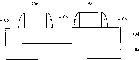
可根据第一较佳实施例加以变化出第三较佳实施例。请参考图4A,第三较佳实施例根据第一较佳实施例所示范的本发明方法来完成绝缘间隙壁410a后,再执行一道回火步骤,而成为如图4B所示的质地更为致密的间隙壁410b。用来强化间隙壁410a在湿式清洗或湿式蚀刻步骤中对蚀刻剂的侧向蚀刻的抵抗力。后续制程如第1较佳实施例中所做的叙述,故不在此赘述。The third preferred embodiment can be changed according to the first preferred embodiment. Please refer to FIG. 4A, the third preferred embodiment completes the insulating spacer 410a according to the method of the present invention demonstrated in the first preferred embodiment, and then performs a tempering step to become a texture as shown in FIG. 4B.
实施例四Embodiment four
可根据第一较佳实施例加以变化出第四较佳实施例。请参考图5A,第四较佳实施例根据第一较佳实施例所示范的本发明方法来完成主动区506的定义并使用如化学气相沉积法(CVD)或其它现有方法来形成绝缘层510a覆盖在主动区506与深埋绝缘层504的暴露面上。绝缘层510a的厚度可介于100至1500之间,且材料可以是各种介电材料,例如氧化物、氮化物或上述材料的任意组合。The fourth preferred embodiment can be changed according to the first preferred embodiment. Please refer to FIG. 5A, the fourth preferred embodiment completes the definition of the
请参考图5B,在完成绝缘层510a后,可先选择性地执行一道回火步骤来使绝缘层510a成为较致密的绝缘层510b。随后再对绝缘层510b进行非等向性蚀刻以产生间隙壁510c,如图5C所示。间隙壁510c用来保护主动区506与暴露出来的深埋绝缘层504的界面,以预防在等向性蚀刻中,主动区506下方发生侧向蚀刻而产生底切问题。后续制程如第1较佳实施例中所做的叙述,故不在此赘述。Referring to FIG. 5B, after the insulating layer 510a is completed, a tempering step may be selectively performed to make the insulating layer 510a become a denser insulating layer 510b. Subsequently, anisotropic etching is performed on the insulating layer 510b to form a
实施例五Embodiment five
综合以上较佳实施例可再加以变化出第五较佳实施例。参考图6A,先如第二较佳实施例的方式,在材料为硅的以定义的主动区606的整个表面上制造一层牺牲氧化层618,例如以热氧化法成长出致密的牺牲氧化层。并选择执行一道回火步骤,使此牺牲氧化层618更为致密作为保护主动区用。Based on the above preferred embodiments, the fifth preferred embodiment can be further changed. Referring to FIG. 6A , as in the second preferred embodiment, a layer of
完成此道牺牲氧化层618后,便可使用如化学气相沉积法(CVD)或其它现有方法来形成一层绝缘层均匀地覆盖在主动区606与深埋绝缘层604的暴露面上。此绝缘层的厚度可约介于100至1500之间,且材料可以是各种介电材料,例如氧化物、氮化物或上述材料的任意组合。After the
请参考图6A,完成绝缘层后,可如第三较佳实施例所示范的,先对绝缘层进行非等向性蚀刻以产生间隙壁610a。随后选择性执行一道回火步骤来使间隙壁610a成为图6B中的质地较致密的间隙壁610b。Please refer to FIG. 6A , after the insulating layer is completed, the insulating layer may be anisotropically etched to form a
或如第四较佳实施例所示范的,在完成绝缘层后,先选择性地执行一道回火步骤来致密化绝缘层。随后再对已致密化的绝缘层进行非等向性蚀刻步骤,而产生如图6B所示的间隙壁610b。Or, as demonstrated in the fourth preferred embodiment, after the insulating layer is completed, a tempering step is selectively performed to densify the insulating layer. Subsequently, an anisotropic etching step is performed on the densified insulating layer to produce a
在完成变化的间隙壁610b后,可用各种一般技术人员所熟知的方式来移除主动区606表面上未被间隙壁610b覆盖的牺牲氧化层618,留下图6B中的牺牲氧化层618c。之后可采用传统制程,如湿浸泡来清洗硅晶圆或移除原生氧化物等步骤。此时,间隙壁610b对主动区606发生保护作用,使得主动区606下方不会产生底切现象。随后在主动区606的表面上可以利用如热氧化法来产生新的闸介电层612。完成闸介电层之后,便可用上述的传统制程进行第一导电层616与第二导电层614的布图来制作闸极。此制作闸极的技术为熟悉此类技术者所熟知,便不在此加以赘述。After the modified
实施例六Embodiment six
本发明制程可整合在传统半导体组件制程,例如金氧半场效晶体管。此处以图7的流程图来说明本发明方法整合至传统半导体制程中的应用。参考图7,提供一SOI晶圆,并在晶圆的磊晶层上形成一层牺牲氧化层,如步骤702所示。此磊晶层的材料可为硅、硅锗或应变硅。随后,参考步骤704,沉积一层罩幕层于牺牲氧化层上,并可如步骤706所示,用现有的微影蚀刻技术将此罩幕层图案化。参考步骤708,根据图案化后的罩幕层,来非等向性蚀刻磊晶层以定义出主动区。The process of the present invention can be integrated into the process of traditional semiconductor components, such as metal oxide semiconductor field effect transistors. Here, the flow chart of FIG. 7 is used to illustrate the application of the method of the present invention integrated into the traditional semiconductor manufacturing process. Referring to FIG. 7 , an SOI wafer is provided, and a sacrificial oxide layer is formed on the epitaxial layer of the wafer, as shown in
完成主动区的定义后,根据本发明方法形成一绝缘层覆盖在主动区与深埋绝缘层的暴露面上,如步骤710所示。之后可视需要来决定如步骤711,先非等向性蚀刻此绝缘层以在主动区侧壁产生间隙壁后,再执行步骤712以回火步骤来致化间隙壁。或是可先执行步骤713的回火步骤来致密化绝缘层后,再执行步骤714以非等向性蚀刻此绝缘层以在主动区侧壁产生间隙壁。After the definition of the active region is completed, an insulating layer is formed to cover the exposed surface of the active region and the buried insulating layer according to the method of the present invention, as shown in
完成间隙壁后,执行步骤716以移除罩幕层。随后可以湿式清洗或湿式蚀刻来除去主动区表面上的原生氧化物或牺牲氧化层,如步骤718所示。最后便可进行传统的半导体制程,如步骤720所示般,在主动区上产生闸氧化层,并进行闸极与源/汲极的制作。After the spacers are completed,
上述各较佳实施例的间隙壁制作,可采反复执行沉积绝缘层与非等向性蚀刻步骤来产生多层结构的间隙壁。此反复沉积与蚀刻的步骤均为现有技艺者所熟悉。For the fabrication of the spacers in the above-mentioned preferred embodiments, the steps of depositing an insulating layer and anisotropic etching can be performed repeatedly to form a multi-layer structure of the spacers. This repeated deposition and etching steps are well known to those skilled in the art.
上述各较佳实施例的回火步骤可以是高温炉管回火步骤(hightemperature furnace anneal)、快速回火步骤(RTA anneal)、氧化步骤(oxidationstep)或上述步骤的任意组合。The tempering step in each of the above preferred embodiments may be a high temperature furnace anneal, a rapid tempering step (RTA anneal), an oxidation step or any combination of the above steps.
此处虽以闸极制作来举例说明本发明方法制作的间隙壁可以预防底切,并避免导电物残留在底切处。但本发明方法亦可适用于各种利用SOI晶圆制造半导体组件的制程中。在深埋绝缘层未被保护材料完全覆盖以前,对于任何制程中会有等向性蚀刻或湿式清洗产生底切可能的步骤,皆适合用本发明方法的改良制程来加以预防。又在深埋绝缘层未被后续所沉积的材料完全覆盖以前,任何导电物的布图步骤,亦可因为使用本发明方法来预防底切产生。也由于预防了底切的产生,故可避免导电物残留在底切处。Here, the fabrication of the gate is used as an example to illustrate that the spacer fabricated by the method of the present invention can prevent undercutting and avoid conductive material remaining at the undercutting. However, the method of the present invention is also applicable to various manufacturing processes of semiconductor components using SOI wafers. Before the deep-buried insulating layer is completely covered by the protective material, the improved process of the method of the present invention can be used to prevent possible undercuts in any process that may be caused by isotropic etching or wet cleaning. Before the deep-buried insulating layer is completely covered by the subsequently deposited material, any conductive patterning step can also be prevented from undercutting by using the method of the present invention. Also because the generation of undercut is prevented, it is possible to avoid conductive material remaining at the undercut.
本发明上述的较佳实施例与较佳实施例的变化应用,可以个别应用或是将所有变化整合起来应用。并且本发明的改良制程可安插在传统制程的深埋绝缘层未被保护材料覆盖以前的任何步骤中。能有效消除或预防主动区侧壁下的深埋绝缘层因受等向性蚀刻或是化学浸泡步骤而产生的底切现象。本发明提供一种有效率、并极为可行的改良制程,来调整利用SOI晶圆来制造半导体组件的传统制程。The above-mentioned preferred embodiments of the present invention and the variant applications of the preferred embodiments can be applied individually or all the variants can be integrated and applied. And the improved process of the present invention can be inserted in any step before the deep-buried insulating layer of the traditional process is not covered by the protective material. It can effectively eliminate or prevent the undercut phenomenon of the deep-buried insulating layer under the side wall of the active region due to isotropic etching or chemical soaking steps. The present invention provides an efficient and highly feasible improved process to adjust the traditional process of using SOI wafers to manufacture semiconductor components.
Claims (20)
Applications Claiming Priority (2)
| Application Number | Priority Date | Filing Date | Title |
|---|---|---|---|
| US10/687,424 US7119023B2 (en) | 2003-10-16 | 2003-10-16 | Process integration of SOI FETs with active layer spacer |
| US10/687,424 | 2003-10-16 |
Publications (2)
| Publication Number | Publication Date |
|---|---|
| CN1716574A true CN1716574A (en) | 2006-01-04 |
| CN100353530C CN100353530C (en) | 2007-12-05 |
Family
ID=34520968
Family Applications (1)
| Application Number | Title | Priority Date | Filing Date |
|---|---|---|---|
| CNB2004100880402A Expired - Lifetime CN100353530C (en) | 2003-10-16 | 2004-10-18 | Method for manufacturing semiconductor components on SOI wafers |
Country Status (2)
| Country | Link |
|---|---|
| US (1) | US7119023B2 (en) |
| CN (1) | CN100353530C (en) |
Cited By (5)
| Publication number | Priority date | Publication date | Assignee | Title |
|---|---|---|---|---|
| CN101373724B (en) * | 2007-08-20 | 2010-05-19 | 中芯国际集成电路制造(上海)有限公司 | Method for determining whether semiconductor device grid undercut dimension being satisfactory or not |
| CN104952886A (en) * | 2015-06-12 | 2015-09-30 | 宁波时代全芯科技有限公司 | Insulating layer silicon-covered structure and preparation method thereof |
| CN107026127A (en) * | 2015-12-09 | 2017-08-08 | 格罗方德半导体公司 | The extension facet high consistency of FDSOI technologies is improved |
| CN108346570A (en) * | 2018-01-24 | 2018-07-31 | 中芯集成电路(宁波)有限公司 | A kind of production method of semiconductor devices |
| CN108598260A (en) * | 2018-05-03 | 2018-09-28 | 中芯集成电路(宁波)有限公司 | Semiconductor structure and forming method thereof |
Families Citing this family (6)
| Publication number | Priority date | Publication date | Assignee | Title |
|---|---|---|---|---|
| US7585716B2 (en) * | 2007-06-27 | 2009-09-08 | International Business Machines Corporation | High-k/metal gate MOSFET with reduced parasitic capacitance |
| US8269312B2 (en) * | 2008-06-05 | 2012-09-18 | Rohm Co., Ltd. | Semiconductor device with resistive element |
| US9698044B2 (en) * | 2011-12-01 | 2017-07-04 | Taiwan Semiconductor Manufacturing Company, Ltd. | Localized carrier lifetime reduction |
| US8883584B2 (en) * | 2012-07-03 | 2014-11-11 | Institute of Microelectronics, Chinese Academy of Sciences | Method of manufacturing semiconductor device with well etched spacer |
| US11634702B2 (en) * | 2018-11-06 | 2023-04-25 | Arizona Board Of Regents On Behalf Of Arizona State University | Cell signaling pathway activation by local AC electric field |
| TWI830206B (en) * | 2021-04-21 | 2024-01-21 | 美商恩特葛瑞斯股份有限公司 | Silicon precursor compounds and method for forming silicon-containing films |
Family Cites Families (14)
| Publication number | Priority date | Publication date | Assignee | Title |
|---|---|---|---|---|
| JPS63237569A (en) * | 1987-03-26 | 1988-10-04 | Nec Corp | Manufacture of mis type semiconductor device |
| US5039621A (en) * | 1990-06-08 | 1991-08-13 | Texas Instruments Incorporated | Semiconductor over insulator mesa and method of forming the same |
| US6979840B1 (en) * | 1991-09-25 | 2005-12-27 | Semiconductor Energy Laboratory Co., Ltd. | Thin film transistors having anodized metal film between the gate wiring and drain wiring |
| US5219783A (en) * | 1992-03-20 | 1993-06-15 | Texas Instruments Incorporated | Method of making semiconductor well structure |
| US5482871A (en) * | 1994-04-15 | 1996-01-09 | Texas Instruments Incorporated | Method for forming a mesa-isolated SOI transistor having a split-process polysilicon gate |
| US5610083A (en) * | 1996-05-20 | 1997-03-11 | Chartered Semiconductor Manufacturing Pte Ltd | Method of making back gate contact for silicon on insulator technology |
| US6004835A (en) * | 1997-04-25 | 1999-12-21 | Micron Technology, Inc. | Method of forming integrated circuitry, conductive lines, a conductive grid, a conductive network, an electrical interconnection to anode location and an electrical interconnection with a transistor source/drain region |
| KR100257517B1 (en) * | 1997-07-01 | 2000-06-01 | 윤종용 | Structure and method of high speed bipolar transistor |
| US6150286A (en) * | 2000-01-03 | 2000-11-21 | Advanced Micro Devices, Inc. | Method of making an ultra thin silicon nitride film |
| US6465296B1 (en) * | 2000-02-22 | 2002-10-15 | Chartered Semiconductor Manufacturing Ltd | Vertical source/drain contact semiconductor |
| JP2001313396A (en) * | 2000-05-01 | 2001-11-09 | Hitachi Ltd | Semiconductor device and its manufacturing method |
| US6657261B2 (en) * | 2001-01-09 | 2003-12-02 | International Business Machines Corporation | Ground-plane device with back oxide topography |
| US6555442B1 (en) | 2002-01-08 | 2003-04-29 | Taiwan Semiconductor Manufacturing Company | Method of forming shallow trench isolation with rounded corner and divot-free by using disposable spacer |
| US6905941B2 (en) * | 2003-06-02 | 2005-06-14 | International Business Machines Corporation | Structure and method to fabricate ultra-thin Si channel devices |
-
2003
- 2003-10-16 US US10/687,424 patent/US7119023B2/en not_active Expired - Lifetime
-
2004
- 2004-10-18 CN CNB2004100880402A patent/CN100353530C/en not_active Expired - Lifetime
Cited By (7)
| Publication number | Priority date | Publication date | Assignee | Title |
|---|---|---|---|---|
| CN101373724B (en) * | 2007-08-20 | 2010-05-19 | 中芯国际集成电路制造(上海)有限公司 | Method for determining whether semiconductor device grid undercut dimension being satisfactory or not |
| CN104952886A (en) * | 2015-06-12 | 2015-09-30 | 宁波时代全芯科技有限公司 | Insulating layer silicon-covered structure and preparation method thereof |
| CN107026127A (en) * | 2015-12-09 | 2017-08-08 | 格罗方德半导体公司 | The extension facet high consistency of FDSOI technologies is improved |
| CN108346570A (en) * | 2018-01-24 | 2018-07-31 | 中芯集成电路(宁波)有限公司 | A kind of production method of semiconductor devices |
| CN108346570B (en) * | 2018-01-24 | 2020-09-04 | 中芯集成电路(宁波)有限公司 | Manufacturing method of semiconductor device |
| CN108598260A (en) * | 2018-05-03 | 2018-09-28 | 中芯集成电路(宁波)有限公司 | Semiconductor structure and forming method thereof |
| CN108598260B (en) * | 2018-05-03 | 2022-03-15 | 中芯集成电路(宁波)有限公司 | Semiconductor structure and forming method thereof |
Also Published As
| Publication number | Publication date |
|---|---|
| US20050085081A1 (en) | 2005-04-21 |
| CN100353530C (en) | 2007-12-05 |
| US7119023B2 (en) | 2006-10-10 |
Similar Documents
| Publication | Publication Date | Title |
|---|---|---|
| CN109786458B (en) | Semiconductor device and method of forming the same | |
| TWI536580B (en) | Fin field effect transistor component and manufacturing method thereof | |
| CN1368756A (en) | Near-surround gate and method of fabricating silicon semiconductor device having same | |
| CN1447986A (en) | Thick oxide layer at the bottom of the channel structure in silicon | |
| CN1695227A (en) | Strained FinFET CMOS device structures | |
| KR20130103272A (en) | Dummy structure for multiple gate dielectric interface and methods | |
| CN104752185B (en) | The forming method of metal gates | |
| CN110581101B (en) | Semiconductor device and method of forming the same | |
| US7655534B2 (en) | Method of forming fin transistor | |
| CN1716574A (en) | Method for manufacturing semiconductor components on SOI wafers | |
| US6432784B1 (en) | Method of forming L-shaped nitride spacers | |
| US10043675B2 (en) | Semiconductor device and method for fabricating the same | |
| KR0137815B1 (en) | Mosfet fabrication | |
| CN109003899A (en) | The forming method of semiconductor structure and forming method thereof, fin formula field effect transistor | |
| CN1649173A (en) | Semiconductor apparatus and method of manufacturing the same | |
| CN118263190A (en) | Method for reducing sidewall loss during trench etching | |
| CN103000688B (en) | Finned-type field-effect transistor structure and finned-type field-effect transistor forming method | |
| CN1270361C (en) | MOS transistor and its manufacture | |
| US9269768B2 (en) | Insulation wall between transistors on SOI | |
| CN114551596B (en) | Semiconductor structure and method for forming the same | |
| TWI244697B (en) | Method of forming a semiconductor device with a SOI wafer | |
| CN102956701B (en) | Structure and forming method of fin type field-effect tube | |
| CN1349250A (en) | Method of forming gate by damascene process | |
| CN111384173B (en) | Preparation method of fin field effect transistor, fin field effect transistor and silicon substrate | |
| KR100596802B1 (en) | Manufacturing method of semiconductor device |
Legal Events
| Date | Code | Title | Description |
|---|---|---|---|
| C06 | Publication | ||
| PB01 | Publication | ||
| C10 | Entry into substantive examination | ||
| SE01 | Entry into force of request for substantive examination | ||
| C14 | Grant of patent or utility model | ||
| GR01 | Patent grant | ||
| CX01 | Expiry of patent term | ||
| CX01 | Expiry of patent term |
Granted publication date: 20071205 |