CN1671255A - display device - Google Patents
display device Download PDFInfo
- Publication number
- CN1671255A CN1671255A CNA2005100558112A CN200510055811A CN1671255A CN 1671255 A CN1671255 A CN 1671255A CN A2005100558112 A CNA2005100558112 A CN A2005100558112A CN 200510055811 A CN200510055811 A CN 200510055811A CN 1671255 A CN1671255 A CN 1671255A
- Authority
- CN
- China
- Prior art keywords
- film
- insulating film
- electrode
- light emitting
- interlayer insulating
- Prior art date
- Legal status (The legal status is an assumption and is not a legal conclusion. Google has not performed a legal analysis and makes no representation as to the accuracy of the status listed.)
- Granted
Links
- 238000005192 partition Methods 0.000 claims abstract description 98
- XLYOFNOQVPJJNP-UHFFFAOYSA-N water Substances O XLYOFNOQVPJJNP-UHFFFAOYSA-N 0.000 claims abstract description 53
- 239000012528 membrane Substances 0.000 claims abstract description 8
- 239000010408 film Substances 0.000 claims description 385
- 239000011229 interlayer Substances 0.000 claims description 145
- 239000000758 substrate Substances 0.000 claims description 73
- 239000010409 thin film Substances 0.000 claims description 58
- 230000035699 permeability Effects 0.000 claims description 46
- 229910052751 metal Inorganic materials 0.000 claims description 11
- 239000002184 metal Substances 0.000 claims description 11
- 230000000694 effects Effects 0.000 abstract description 8
- 230000000149 penetrating effect Effects 0.000 abstract description 8
- 238000007789 sealing Methods 0.000 abstract description 7
- 238000009413 insulation Methods 0.000 abstract 2
- 239000010410 layer Substances 0.000 description 138
- 239000000463 material Substances 0.000 description 96
- 239000004065 semiconductor Substances 0.000 description 37
- 239000003566 sealing material Substances 0.000 description 28
- -1 siloxanes Chemical class 0.000 description 27
- IJGRMHOSHXDMSA-UHFFFAOYSA-N Atomic nitrogen Chemical compound N#N IJGRMHOSHXDMSA-UHFFFAOYSA-N 0.000 description 23
- VYPSYNLAJGMNEJ-UHFFFAOYSA-N Silicium dioxide Chemical compound O=[Si]=O VYPSYNLAJGMNEJ-UHFFFAOYSA-N 0.000 description 21
- 238000002347 injection Methods 0.000 description 20
- 239000007924 injection Substances 0.000 description 20
- 229910052814 silicon oxide Inorganic materials 0.000 description 19
- 239000000126 substance Substances 0.000 description 18
- 229910052581 Si3N4 Inorganic materials 0.000 description 17
- HQVNEWCFYHHQES-UHFFFAOYSA-N silicon nitride Chemical compound N12[Si]34N5[Si]62N3[Si]51N64 HQVNEWCFYHHQES-UHFFFAOYSA-N 0.000 description 17
- 239000011159 matrix material Substances 0.000 description 12
- 229910052760 oxygen Inorganic materials 0.000 description 12
- 229910052782 aluminium Inorganic materials 0.000 description 11
- 239000004642 Polyimide Substances 0.000 description 10
- XUIMIQQOPSSXEZ-UHFFFAOYSA-N Silicon Chemical compound [Si] XUIMIQQOPSSXEZ-UHFFFAOYSA-N 0.000 description 10
- 230000002411 adverse Effects 0.000 description 10
- XAGFODPZIPBFFR-UHFFFAOYSA-N aluminium Chemical compound [Al] XAGFODPZIPBFFR-UHFFFAOYSA-N 0.000 description 10
- QVGXLLKOCUKJST-UHFFFAOYSA-N atomic oxygen Chemical compound [O] QVGXLLKOCUKJST-UHFFFAOYSA-N 0.000 description 10
- 239000002585 base Substances 0.000 description 10
- 239000002274 desiccant Substances 0.000 description 10
- 230000005525 hole transport Effects 0.000 description 10
- 238000000034 method Methods 0.000 description 10
- 229910052757 nitrogen Inorganic materials 0.000 description 10
- 239000001301 oxygen Substances 0.000 description 10
- 229920001721 polyimide Polymers 0.000 description 10
- 229910052710 silicon Inorganic materials 0.000 description 10
- 239000010703 silicon Substances 0.000 description 10
- NIXOWILDQLNWCW-UHFFFAOYSA-N acrylic acid group Chemical group C(C=C)(=O)O NIXOWILDQLNWCW-UHFFFAOYSA-N 0.000 description 9
- 230000000052 comparative effect Effects 0.000 description 9
- 230000002829 reductive effect Effects 0.000 description 9
- 239000011368 organic material Substances 0.000 description 8
- 230000002093 peripheral effect Effects 0.000 description 8
- 239000002356 single layer Substances 0.000 description 8
- 229910021417 amorphous silicon Inorganic materials 0.000 description 7
- KPUWHANPEXNPJT-UHFFFAOYSA-N disiloxane Chemical class [SiH3]O[SiH3] KPUWHANPEXNPJT-UHFFFAOYSA-N 0.000 description 7
- 238000010438 heat treatment Methods 0.000 description 7
- 150000002894 organic compounds Chemical class 0.000 description 7
- 239000010936 titanium Substances 0.000 description 7
- 229910052719 titanium Inorganic materials 0.000 description 7
- UHOVQNZJYSORNB-UHFFFAOYSA-N Benzene Chemical group C1=CC=CC=C1 UHOVQNZJYSORNB-UHFFFAOYSA-N 0.000 description 6
- RTAQQCXQSZGOHL-UHFFFAOYSA-N Titanium Chemical compound [Ti] RTAQQCXQSZGOHL-UHFFFAOYSA-N 0.000 description 6
- XLOMVQKBTHCTTD-UHFFFAOYSA-N Zinc monoxide Chemical compound [Zn]=O XLOMVQKBTHCTTD-UHFFFAOYSA-N 0.000 description 6
- 238000002425 crystallisation Methods 0.000 description 6
- 230000008025 crystallization Effects 0.000 description 6
- 239000012535 impurity Substances 0.000 description 6
- 239000000203 mixture Substances 0.000 description 6
- 229920000172 poly(styrenesulfonic acid) Polymers 0.000 description 6
- 230000002441 reversible effect Effects 0.000 description 6
- 238000004544 sputter deposition Methods 0.000 description 6
- 229910010272 inorganic material Inorganic materials 0.000 description 5
- 238000004519 manufacturing process Methods 0.000 description 5
- 239000000049 pigment Substances 0.000 description 5
- 229920000553 poly(phenylenevinylene) Polymers 0.000 description 5
- 229940005642 polystyrene sulfonic acid Drugs 0.000 description 5
- 229920005989 resin Polymers 0.000 description 5
- 239000011347 resin Substances 0.000 description 5
- MIOPJNTWMNEORI-GMSGAONNSA-N (S)-camphorsulfonic acid Chemical compound C1C[C@@]2(CS(O)(=O)=O)C(=O)C[C@@H]1C2(C)C MIOPJNTWMNEORI-GMSGAONNSA-N 0.000 description 4
- XKRFYHLGVUSROY-UHFFFAOYSA-N Argon Chemical compound [Ar] XKRFYHLGVUSROY-UHFFFAOYSA-N 0.000 description 4
- OKTJSMMVPCPJKN-UHFFFAOYSA-N Carbon Chemical compound [C] OKTJSMMVPCPJKN-UHFFFAOYSA-N 0.000 description 4
- 229920001609 Poly(3,4-ethylenedioxythiophene) Polymers 0.000 description 4
- 229920000265 Polyparaphenylene Polymers 0.000 description 4
- 239000007983 Tris buffer Substances 0.000 description 4
- XJHCXCQVJFPJIK-UHFFFAOYSA-M caesium fluoride Chemical compound [F-].[Cs+] XJHCXCQVJFPJIK-UHFFFAOYSA-M 0.000 description 4
- 229910052799 carbon Inorganic materials 0.000 description 4
- 150000001875 compounds Chemical class 0.000 description 4
- 238000005530 etching Methods 0.000 description 4
- 230000005284 excitation Effects 0.000 description 4
- 239000007789 gas Substances 0.000 description 4
- 239000011521 glass Substances 0.000 description 4
- 229910052739 hydrogen Inorganic materials 0.000 description 4
- 238000010030 laminating Methods 0.000 description 4
- 229910052750 molybdenum Inorganic materials 0.000 description 4
- 238000002161 passivation Methods 0.000 description 4
- BASFCYQUMIYNBI-UHFFFAOYSA-N platinum Chemical compound [Pt] BASFCYQUMIYNBI-UHFFFAOYSA-N 0.000 description 4
- 229920003227 poly(N-vinyl carbazole) Polymers 0.000 description 4
- 229920000767 polyaniline Polymers 0.000 description 4
- 229920002098 polyfluorene Polymers 0.000 description 4
- 229920000123 polythiophene Polymers 0.000 description 4
- 238000004528 spin coating Methods 0.000 description 4
- 238000007740 vapor deposition Methods 0.000 description 4
- UFHFLCQGNIYNRP-UHFFFAOYSA-N Hydrogen Chemical compound [H][H] UFHFLCQGNIYNRP-UHFFFAOYSA-N 0.000 description 3
- 229910015711 MoOx Inorganic materials 0.000 description 3
- ZOKXTWBITQBERF-UHFFFAOYSA-N Molybdenum Chemical compound [Mo] ZOKXTWBITQBERF-UHFFFAOYSA-N 0.000 description 3
- 229910052783 alkali metal Inorganic materials 0.000 description 3
- 150000001340 alkali metals Chemical class 0.000 description 3
- 229910052784 alkaline earth metal Inorganic materials 0.000 description 3
- 150000001342 alkaline earth metals Chemical class 0.000 description 3
- 229910052802 copper Inorganic materials 0.000 description 3
- 239000010949 copper Substances 0.000 description 3
- VBVAVBCYMYWNOU-UHFFFAOYSA-N coumarin 6 Chemical compound C1=CC=C2SC(C3=CC4=CC=C(C=C4OC3=O)N(CC)CC)=NC2=C1 VBVAVBCYMYWNOU-UHFFFAOYSA-N 0.000 description 3
- 239000013078 crystal Substances 0.000 description 3
- 229910021419 crystalline silicon Inorganic materials 0.000 description 3
- 230000000994 depressogenic effect Effects 0.000 description 3
- 238000010586 diagram Methods 0.000 description 3
- 238000005265 energy consumption Methods 0.000 description 3
- 239000001257 hydrogen Substances 0.000 description 3
- 239000011147 inorganic material Substances 0.000 description 3
- 239000011733 molybdenum Substances 0.000 description 3
- VOFUROIFQGPCGE-UHFFFAOYSA-N nile red Chemical compound C1=CC=C2C3=NC4=CC=C(N(CC)CC)C=C4OC3=CC(=O)C2=C1 VOFUROIFQGPCGE-UHFFFAOYSA-N 0.000 description 3
- 239000012466 permeate Substances 0.000 description 3
- 238000005268 plasma chemical vapour deposition Methods 0.000 description 3
- 229910021332 silicide Inorganic materials 0.000 description 3
- FVBUAEGBCNSCDD-UHFFFAOYSA-N silicide(4-) Chemical group [Si-4] FVBUAEGBCNSCDD-UHFFFAOYSA-N 0.000 description 3
- 239000000243 solution Substances 0.000 description 3
- 125000001424 substituent group Chemical group 0.000 description 3
- 239000011787 zinc oxide Substances 0.000 description 3
- 150000005072 1,3,4-oxadiazoles Chemical class 0.000 description 2
- IYZMXHQDXZKNCY-UHFFFAOYSA-N 1-n,1-n-diphenyl-4-n,4-n-bis[4-(n-phenylanilino)phenyl]benzene-1,4-diamine Chemical compound C1=CC=CC=C1N(C=1C=CC(=CC=1)N(C=1C=CC(=CC=1)N(C=1C=CC=CC=1)C=1C=CC=CC=1)C=1C=CC(=CC=1)N(C=1C=CC=CC=1)C=1C=CC=CC=1)C1=CC=CC=C1 IYZMXHQDXZKNCY-UHFFFAOYSA-N 0.000 description 2
- RYGMFSIKBFXOCR-UHFFFAOYSA-N Copper Chemical compound [Cu] RYGMFSIKBFXOCR-UHFFFAOYSA-N 0.000 description 2
- GYHNNYVSQQEPJS-UHFFFAOYSA-N Gallium Chemical compound [Ga] GYHNNYVSQQEPJS-UHFFFAOYSA-N 0.000 description 2
- PXHVJJICTQNCMI-UHFFFAOYSA-N Nickel Chemical compound [Ni] PXHVJJICTQNCMI-UHFFFAOYSA-N 0.000 description 2
- KDLHZDBZIXYQEI-UHFFFAOYSA-N Palladium Chemical compound [Pd] KDLHZDBZIXYQEI-UHFFFAOYSA-N 0.000 description 2
- OAICVXFJPJFONN-UHFFFAOYSA-N Phosphorus Chemical compound [P] OAICVXFJPJFONN-UHFFFAOYSA-N 0.000 description 2
- 229920000282 Poly(3-cyclohexylthiophene) Polymers 0.000 description 2
- 229920000291 Poly(9,9-dioctylfluorene) Polymers 0.000 description 2
- 229910000577 Silicon-germanium Inorganic materials 0.000 description 2
- PPBRXRYQALVLMV-UHFFFAOYSA-N Styrene Chemical compound C=CC1=CC=CC=C1 PPBRXRYQALVLMV-UHFFFAOYSA-N 0.000 description 2
- NRTOMJZYCJJWKI-UHFFFAOYSA-N Titanium nitride Chemical compound [Ti]#N NRTOMJZYCJJWKI-UHFFFAOYSA-N 0.000 description 2
- LEVVHYCKPQWKOP-UHFFFAOYSA-N [Si].[Ge] Chemical compound [Si].[Ge] LEVVHYCKPQWKOP-UHFFFAOYSA-N 0.000 description 2
- 239000000956 alloy Substances 0.000 description 2
- 229910052786 argon Inorganic materials 0.000 description 2
- 230000008901 benefit Effects 0.000 description 2
- 230000000903 blocking effect Effects 0.000 description 2
- 230000008859 change Effects 0.000 description 2
- 239000003795 chemical substances by application Substances 0.000 description 2
- 239000011248 coating agent Substances 0.000 description 2
- 238000000576 coating method Methods 0.000 description 2
- 150000004696 coordination complex Chemical class 0.000 description 2
- 238000001723 curing Methods 0.000 description 2
- 230000007547 defect Effects 0.000 description 2
- 239000000945 filler Substances 0.000 description 2
- 229910052733 gallium Inorganic materials 0.000 description 2
- RBTKNAXYKSUFRK-UHFFFAOYSA-N heliogen blue Chemical compound [Cu].[N-]1C2=C(C=CC=C3)C3=C1N=C([N-]1)C3=CC=CC=C3C1=NC([N-]1)=C(C=CC=C3)C3=C1N=C([N-]1)C3=CC=CC=C3C1=N2 RBTKNAXYKSUFRK-UHFFFAOYSA-N 0.000 description 2
- AMWRITDGCCNYAT-UHFFFAOYSA-L hydroxy(oxo)manganese;manganese Chemical compound [Mn].O[Mn]=O.O[Mn]=O AMWRITDGCCNYAT-UHFFFAOYSA-L 0.000 description 2
- 239000011261 inert gas Substances 0.000 description 2
- 150000002484 inorganic compounds Chemical class 0.000 description 2
- 239000011810 insulating material Substances 0.000 description 2
- 230000007774 longterm Effects 0.000 description 2
- 239000011777 magnesium Substances 0.000 description 2
- 229910000476 molybdenum oxide Inorganic materials 0.000 description 2
- IBHBKWKFFTZAHE-UHFFFAOYSA-N n-[4-[4-(n-naphthalen-1-ylanilino)phenyl]phenyl]-n-phenylnaphthalen-1-amine Chemical group C1=CC=CC=C1N(C=1C2=CC=CC=C2C=CC=1)C1=CC=C(C=2C=CC(=CC=2)N(C=2C=CC=CC=2)C=2C3=CC=CC=C3C=CC=2)C=C1 IBHBKWKFFTZAHE-UHFFFAOYSA-N 0.000 description 2
- QJGQUHMNIGDVPM-UHFFFAOYSA-N nitrogen group Chemical group [N] QJGQUHMNIGDVPM-UHFFFAOYSA-N 0.000 description 2
- MWUXSHHQAYIFBG-UHFFFAOYSA-N nitrogen oxide Inorganic materials O=[N] MWUXSHHQAYIFBG-UHFFFAOYSA-N 0.000 description 2
- 239000003960 organic solvent Substances 0.000 description 2
- PQQKPALAQIIWST-UHFFFAOYSA-N oxomolybdenum Chemical compound [Mo]=O PQQKPALAQIIWST-UHFFFAOYSA-N 0.000 description 2
- 229960003540 oxyquinoline Drugs 0.000 description 2
- 229910052698 phosphorus Inorganic materials 0.000 description 2
- 239000011574 phosphorus Substances 0.000 description 2
- 229920002120 photoresistant polymer Polymers 0.000 description 2
- IEQIEDJGQAUEQZ-UHFFFAOYSA-N phthalocyanine Chemical compound N1C(N=C2C3=CC=CC=C3C(N=C3C4=CC=CC=C4C(=N4)N3)=N2)=C(C=CC=C2)C2=C1N=C1C2=CC=CC=C2C4=N1 IEQIEDJGQAUEQZ-UHFFFAOYSA-N 0.000 description 2
- 229910052697 platinum Inorganic materials 0.000 description 2
- 229920000301 poly(3-hexylthiophene-2,5-diyl) polymer Polymers 0.000 description 2
- 229920001296 polysiloxane Polymers 0.000 description 2
- 239000010453 quartz Substances 0.000 description 2
- MCJGNVYPOGVAJF-UHFFFAOYSA-N quinolin-8-ol Chemical compound C1=CN=C2C(O)=CC=CC2=C1 MCJGNVYPOGVAJF-UHFFFAOYSA-N 0.000 description 2
- 230000009467 reduction Effects 0.000 description 2
- 229910052721 tungsten Inorganic materials 0.000 description 2
- DTZWGKCFKSJGPK-VOTSOKGWSA-N (e)-2-(2-methyl-6-(2-(1,1,7,7-tetramethyl-1,2,3,5,6,7-hexahydropyrido[3,2,1-ij]quinolin-9-yl)vinyl)-4h-pyran-4-ylidene)malononitrile Chemical compound O1C(C)=CC(=C(C#N)C#N)C=C1\C=C\C1=CC(C(CCN2CCC3(C)C)(C)C)=C2C3=C1 DTZWGKCFKSJGPK-VOTSOKGWSA-N 0.000 description 1
- KLCLIOISYBHYDZ-UHFFFAOYSA-N 1,4,4-triphenylbuta-1,3-dienylbenzene Chemical compound C=1C=CC=CC=1C(C=1C=CC=CC=1)=CC=C(C=1C=CC=CC=1)C1=CC=CC=C1 KLCLIOISYBHYDZ-UHFFFAOYSA-N 0.000 description 1
- YEWTUGLUENRXFN-UHFFFAOYSA-N 3-(4-octylphenyl)-2-thiophen-2-ylthiophene Chemical compound C1=CC(CCCCCCCC)=CC=C1C1=C(C=2SC=CC=2)SC=C1 YEWTUGLUENRXFN-UHFFFAOYSA-N 0.000 description 1
- CHMILGIDWWDNMF-UHFFFAOYSA-N 3-(4-octylphenyl)thiophene Chemical compound C1=CC(CCCCCCCC)=CC=C1C1=CSC=C1 CHMILGIDWWDNMF-UHFFFAOYSA-N 0.000 description 1
- OGGKVJMNFFSDEV-UHFFFAOYSA-N 3-methyl-n-[4-[4-(n-(3-methylphenyl)anilino)phenyl]phenyl]-n-phenylaniline Chemical group CC1=CC=CC(N(C=2C=CC=CC=2)C=2C=CC(=CC=2)C=2C=CC(=CC=2)N(C=2C=CC=CC=2)C=2C=C(C)C=CC=2)=C1 OGGKVJMNFFSDEV-UHFFFAOYSA-N 0.000 description 1
- SCZWJXTUYYSKGF-UHFFFAOYSA-N 5,12-dimethylquinolino[2,3-b]acridine-7,14-dione Chemical compound CN1C2=CC=CC=C2C(=O)C2=C1C=C1C(=O)C3=CC=CC=C3N(C)C1=C2 SCZWJXTUYYSKGF-UHFFFAOYSA-N 0.000 description 1
- VIZUPBYFLORCRA-UHFFFAOYSA-N 9,10-dinaphthalen-2-ylanthracene Chemical compound C12=CC=CC=C2C(C2=CC3=CC=CC=C3C=C2)=C(C=CC=C2)C2=C1C1=CC=C(C=CC=C2)C2=C1 VIZUPBYFLORCRA-UHFFFAOYSA-N 0.000 description 1
- FCNCGHJSNVOIKE-UHFFFAOYSA-N 9,10-diphenylanthracene Chemical compound C1=CC=CC=C1C(C1=CC=CC=C11)=C(C=CC=C2)C2=C1C1=CC=CC=C1 FCNCGHJSNVOIKE-UHFFFAOYSA-N 0.000 description 1
- ZOXJGFHDIHLPTG-UHFFFAOYSA-N Boron Chemical compound [B] ZOXJGFHDIHLPTG-UHFFFAOYSA-N 0.000 description 1
- MSDMPJCOOXURQD-UHFFFAOYSA-N C545T Chemical compound C1=CC=C2SC(C3=CC=4C=C5C6=C(C=4OC3=O)C(C)(C)CCN6CCC5(C)C)=NC2=C1 MSDMPJCOOXURQD-UHFFFAOYSA-N 0.000 description 1
- 239000004593 Epoxy Substances 0.000 description 1
- 239000004838 Heat curing adhesive Substances 0.000 description 1
- FYYHWMGAXLPEAU-UHFFFAOYSA-N Magnesium Chemical compound [Mg] FYYHWMGAXLPEAU-UHFFFAOYSA-N 0.000 description 1
- 229910052779 Neodymium Inorganic materials 0.000 description 1
- GOZPTOHMTKTIQP-UHFFFAOYSA-N OC1=CC=CC2=CC=C3C=CC(=NC3=C21)C(=O)O Chemical compound OC1=CC=CC2=CC=C3C=CC(=NC3=C21)C(=O)O GOZPTOHMTKTIQP-UHFFFAOYSA-N 0.000 description 1
- 239000004695 Polyether sulfone Substances 0.000 description 1
- 238000001237 Raman spectrum Methods 0.000 description 1
- 229910003902 SiCl 4 Inorganic materials 0.000 description 1
- 229910002808 Si–O–Si Inorganic materials 0.000 description 1
- 229910000831 Steel Inorganic materials 0.000 description 1
- ATJFFYVFTNAWJD-UHFFFAOYSA-N Tin Chemical compound [Sn] ATJFFYVFTNAWJD-UHFFFAOYSA-N 0.000 description 1
- 238000002441 X-ray diffraction Methods 0.000 description 1
- HCHKCACWOHOZIP-UHFFFAOYSA-N Zinc Chemical compound [Zn] HCHKCACWOHOZIP-UHFFFAOYSA-N 0.000 description 1
- XHCLAFWTIXFWPH-UHFFFAOYSA-N [O-2].[O-2].[O-2].[O-2].[O-2].[V+5].[V+5] Chemical compound [O-2].[O-2].[O-2].[O-2].[O-2].[V+5].[V+5] XHCLAFWTIXFWPH-UHFFFAOYSA-N 0.000 description 1
- 239000002253 acid Substances 0.000 description 1
- 239000000853 adhesive Substances 0.000 description 1
- 230000001070 adhesive effect Effects 0.000 description 1
- 150000001341 alkaline earth metal compounds Chemical class 0.000 description 1
- 125000000217 alkyl group Chemical group 0.000 description 1
- 229910045601 alloy Inorganic materials 0.000 description 1
- 239000007864 aqueous solution Substances 0.000 description 1
- 150000004982 aromatic amines Chemical class 0.000 description 1
- 150000004984 aromatic diamines Chemical class 0.000 description 1
- 150000004945 aromatic hydrocarbons Chemical class 0.000 description 1
- WZJYKHNJTSNBHV-UHFFFAOYSA-N benzo[h]quinoline Chemical group C1=CN=C2C3=CC=CC=C3C=CC2=C1 WZJYKHNJTSNBHV-UHFFFAOYSA-N 0.000 description 1
- 229910052790 beryllium Inorganic materials 0.000 description 1
- ATBAMAFKBVZNFJ-UHFFFAOYSA-N beryllium atom Chemical compound [Be] ATBAMAFKBVZNFJ-UHFFFAOYSA-N 0.000 description 1
- UFVXQDWNSAGPHN-UHFFFAOYSA-K bis[(2-methylquinolin-8-yl)oxy]-(4-phenylphenoxy)alumane Chemical compound [Al+3].C1=CC=C([O-])C2=NC(C)=CC=C21.C1=CC=C([O-])C2=NC(C)=CC=C21.C1=CC([O-])=CC=C1C1=CC=CC=C1 UFVXQDWNSAGPHN-UHFFFAOYSA-K 0.000 description 1
- 229910052796 boron Inorganic materials 0.000 description 1
- DQXBYHZEEUGOBF-UHFFFAOYSA-N but-3-enoic acid;ethene Chemical compound C=C.OC(=O)CC=C DQXBYHZEEUGOBF-UHFFFAOYSA-N 0.000 description 1
- WUKWITHWXAAZEY-UHFFFAOYSA-L calcium difluoride Chemical compound [F-].[F-].[Ca+2] WUKWITHWXAAZEY-UHFFFAOYSA-L 0.000 description 1
- 239000003990 capacitor Substances 0.000 description 1
- 230000015556 catabolic process Effects 0.000 description 1
- 239000003054 catalyst Substances 0.000 description 1
- SLLGVCUQYRMELA-UHFFFAOYSA-N chlorosilicon Chemical compound Cl[Si] SLLGVCUQYRMELA-UHFFFAOYSA-N 0.000 description 1
- 229910052804 chromium Inorganic materials 0.000 description 1
- 229910017052 cobalt Inorganic materials 0.000 description 1
- 239000010941 cobalt Substances 0.000 description 1
- GUTLYIVDDKVIGB-UHFFFAOYSA-N cobalt atom Chemical compound [Co] GUTLYIVDDKVIGB-UHFFFAOYSA-N 0.000 description 1
- 239000003086 colorant Substances 0.000 description 1
- 239000002131 composite material Substances 0.000 description 1
- 239000000470 constituent Substances 0.000 description 1
- 239000013039 cover film Substances 0.000 description 1
- 238000005520 cutting process Methods 0.000 description 1
- 238000000354 decomposition reaction Methods 0.000 description 1
- 230000003247 decreasing effect Effects 0.000 description 1
- 238000006731 degradation reaction Methods 0.000 description 1
- 238000000151 deposition Methods 0.000 description 1
- 238000009792 diffusion process Methods 0.000 description 1
- BKMIWBZIQAAZBD-UHFFFAOYSA-N diindenoperylene Chemical compound C12=C3C4=CC=C2C2=CC=CC=C2C1=CC=C3C1=CC=C2C3=CC=CC=C3C3=CC=C4C1=C32 BKMIWBZIQAAZBD-UHFFFAOYSA-N 0.000 description 1
- 238000007865 diluting Methods 0.000 description 1
- 238000010790 dilution Methods 0.000 description 1
- 239000012895 dilution Substances 0.000 description 1
- 239000002019 doping agent Substances 0.000 description 1
- 230000009977 dual effect Effects 0.000 description 1
- 238000005401 electroluminescence Methods 0.000 description 1
- 239000008393 encapsulating agent Substances 0.000 description 1
- 239000005038 ethylene vinyl acetate Substances 0.000 description 1
- 238000002474 experimental method Methods 0.000 description 1
- 230000005669 field effect Effects 0.000 description 1
- 238000010304 firing Methods 0.000 description 1
- 229910052731 fluorine Inorganic materials 0.000 description 1
- 125000001153 fluoro group Chemical group F* 0.000 description 1
- 229910052732 germanium Inorganic materials 0.000 description 1
- GNPVGFCGXDBREM-UHFFFAOYSA-N germanium atom Chemical compound [Ge] GNPVGFCGXDBREM-UHFFFAOYSA-N 0.000 description 1
- PCHJSUWPFVWCPO-UHFFFAOYSA-N gold Chemical compound [Au] PCHJSUWPFVWCPO-UHFFFAOYSA-N 0.000 description 1
- 229910052737 gold Inorganic materials 0.000 description 1
- 239000010931 gold Substances 0.000 description 1
- 229910052736 halogen Inorganic materials 0.000 description 1
- 150000002367 halogens Chemical class 0.000 description 1
- 239000001307 helium Substances 0.000 description 1
- 229910052734 helium Inorganic materials 0.000 description 1
- SWQJXJOGLNCZEY-UHFFFAOYSA-N helium atom Chemical compound [He] SWQJXJOGLNCZEY-UHFFFAOYSA-N 0.000 description 1
- 125000004435 hydrogen atom Chemical group [H]* 0.000 description 1
- 229910003437 indium oxide Inorganic materials 0.000 description 1
- PJXISJQVUVHSOJ-UHFFFAOYSA-N indium(iii) oxide Chemical compound [O-2].[O-2].[O-2].[In+3].[In+3] PJXISJQVUVHSOJ-UHFFFAOYSA-N 0.000 description 1
- AMGQUBHHOARCQH-UHFFFAOYSA-N indium;oxotin Chemical compound [In].[Sn]=O AMGQUBHHOARCQH-UHFFFAOYSA-N 0.000 description 1
- 238000007641 inkjet printing Methods 0.000 description 1
- 238000003780 insertion Methods 0.000 description 1
- 230000037431 insertion Effects 0.000 description 1
- 150000002500 ions Chemical class 0.000 description 1
- 229910052741 iridium Inorganic materials 0.000 description 1
- GKOZUEZYRPOHIO-UHFFFAOYSA-N iridium atom Chemical compound [Ir] GKOZUEZYRPOHIO-UHFFFAOYSA-N 0.000 description 1
- 229910052743 krypton Inorganic materials 0.000 description 1
- DNNSSWSSYDEUBZ-UHFFFAOYSA-N krypton atom Chemical compound [Kr] DNNSSWSSYDEUBZ-UHFFFAOYSA-N 0.000 description 1
- 238000005499 laser crystallization Methods 0.000 description 1
- 239000011133 lead Substances 0.000 description 1
- 239000004973 liquid crystal related substance Substances 0.000 description 1
- PQXKHYXIUOZZFA-UHFFFAOYSA-M lithium fluoride Chemical compound [Li+].[F-] PQXKHYXIUOZZFA-UHFFFAOYSA-M 0.000 description 1
- 229910052749 magnesium Inorganic materials 0.000 description 1
- 229910044991 metal oxide Inorganic materials 0.000 description 1
- 150000004706 metal oxides Chemical class 0.000 description 1
- 239000013081 microcrystal Substances 0.000 description 1
- NMVZHJHQIMLNBM-UHFFFAOYSA-N n,n-dimethyl-4-[2-(6-methyl-4h-pyran-2-yl)ethenyl]aniline Chemical compound C1=CC(N(C)C)=CC=C1C=CC1=CCC=C(C)O1 NMVZHJHQIMLNBM-UHFFFAOYSA-N 0.000 description 1
- 229910052754 neon Inorganic materials 0.000 description 1
- GKAOGPIIYCISHV-UHFFFAOYSA-N neon atom Chemical compound [Ne] GKAOGPIIYCISHV-UHFFFAOYSA-N 0.000 description 1
- 230000003472 neutralizing effect Effects 0.000 description 1
- 229910052759 nickel Inorganic materials 0.000 description 1
- QGLKJKCYBOYXKC-UHFFFAOYSA-N nonaoxidotritungsten Chemical compound O=[W]1(=O)O[W](=O)(=O)O[W](=O)(=O)O1 QGLKJKCYBOYXKC-UHFFFAOYSA-N 0.000 description 1
- 230000003287 optical effect Effects 0.000 description 1
- 125000002524 organometallic group Chemical group 0.000 description 1
- JMANVNJQNLATNU-UHFFFAOYSA-N oxalonitrile Chemical compound N#CC#N JMANVNJQNLATNU-UHFFFAOYSA-N 0.000 description 1
- 229910052763 palladium Inorganic materials 0.000 description 1
- 239000002245 particle Substances 0.000 description 1
- 230000035515 penetration Effects 0.000 description 1
- 230000000737 periodic effect Effects 0.000 description 1
- 238000002294 plasma sputter deposition Methods 0.000 description 1
- 229920003023 plastic Polymers 0.000 description 1
- 239000004033 plastic Substances 0.000 description 1
- 229920001200 poly(ethylene-vinyl acetate) Polymers 0.000 description 1
- 229920002037 poly(vinyl butyral) polymer Polymers 0.000 description 1
- 229920000058 polyacrylate Polymers 0.000 description 1
- 229920000515 polycarbonate Polymers 0.000 description 1
- 239000004417 polycarbonate Substances 0.000 description 1
- 229910021420 polycrystalline silicon Inorganic materials 0.000 description 1
- 229920006393 polyether sulfone Polymers 0.000 description 1
- 239000005020 polyethylene terephthalate Substances 0.000 description 1
- 229920000139 polyethylene terephthalate Polymers 0.000 description 1
- 229920000642 polymer Polymers 0.000 description 1
- 229920005591 polysilicon Polymers 0.000 description 1
- 239000004800 polyvinyl chloride Substances 0.000 description 1
- 229920000915 polyvinyl chloride Polymers 0.000 description 1
- 230000008569 process Effects 0.000 description 1
- 230000000750 progressive effect Effects 0.000 description 1
- 230000001737 promoting effect Effects 0.000 description 1
- 230000001681 protective effect Effects 0.000 description 1
- 125000002943 quinolinyl group Chemical group N1=C(C=CC2=CC=CC=C12)* 0.000 description 1
- 230000005855 radiation Effects 0.000 description 1
- 229910001925 ruthenium oxide Inorganic materials 0.000 description 1
- WOCIAKWEIIZHES-UHFFFAOYSA-N ruthenium(iv) oxide Chemical compound O=[Ru]=O WOCIAKWEIIZHES-UHFFFAOYSA-N 0.000 description 1
- 239000010959 steel Substances 0.000 description 1
- 229910052715 tantalum Inorganic materials 0.000 description 1
- RPVGLMKJGQMQSN-UHFFFAOYSA-N tiliquinol Chemical compound C1=CC=C2C(C)=CC=C(O)C2=N1 RPVGLMKJGQMQSN-UHFFFAOYSA-N 0.000 description 1
- 229910052718 tin Inorganic materials 0.000 description 1
- 239000011135 tin Substances 0.000 description 1
- 230000007704 transition Effects 0.000 description 1
- 238000002834 transmittance Methods 0.000 description 1
- LENZDBCJOHFCAS-UHFFFAOYSA-N tris Chemical compound OCC(N)(CO)CO LENZDBCJOHFCAS-UHFFFAOYSA-N 0.000 description 1
- WFKWXMTUELFFGS-UHFFFAOYSA-N tungsten Chemical compound [W] WFKWXMTUELFFGS-UHFFFAOYSA-N 0.000 description 1
- 239000010937 tungsten Substances 0.000 description 1
- 229910001930 tungsten oxide Inorganic materials 0.000 description 1
- 229910001935 vanadium oxide Inorganic materials 0.000 description 1
- 229920002554 vinyl polymer Polymers 0.000 description 1
- 229910052725 zinc Inorganic materials 0.000 description 1
- 239000011701 zinc Substances 0.000 description 1
- YVTHLONGBIQYBO-UHFFFAOYSA-N zinc indium(3+) oxygen(2-) Chemical compound [O--].[Zn++].[In+3] YVTHLONGBIQYBO-UHFFFAOYSA-N 0.000 description 1
Images


Classifications
-
- H—ELECTRICITY
- H10—SEMICONDUCTOR DEVICES; ELECTRIC SOLID-STATE DEVICES NOT OTHERWISE PROVIDED FOR
- H10K—ORGANIC ELECTRIC SOLID-STATE DEVICES
- H10K59/00—Integrated devices, or assemblies of multiple devices, comprising at least one organic light-emitting element covered by group H10K50/00
- H10K59/10—OLED displays
- H10K59/12—Active-matrix OLED [AMOLED] displays
- H10K59/122—Pixel-defining structures or layers, e.g. banks
-
- H—ELECTRICITY
- H10—SEMICONDUCTOR DEVICES; ELECTRIC SOLID-STATE DEVICES NOT OTHERWISE PROVIDED FOR
- H10K—ORGANIC ELECTRIC SOLID-STATE DEVICES
- H10K59/00—Integrated devices, or assemblies of multiple devices, comprising at least one organic light-emitting element covered by group H10K50/00
- H10K59/10—OLED displays
- H10K59/12—Active-matrix OLED [AMOLED] displays
- H10K59/124—Insulating layers formed between TFT elements and OLED elements
-
- H—ELECTRICITY
- H10—SEMICONDUCTOR DEVICES; ELECTRIC SOLID-STATE DEVICES NOT OTHERWISE PROVIDED FOR
- H10K—ORGANIC ELECTRIC SOLID-STATE DEVICES
- H10K50/00—Organic light-emitting devices
- H10K50/80—Constructional details
- H10K50/805—Electrodes
- H10K50/82—Cathodes
- H10K50/828—Transparent cathodes, e.g. comprising thin metal layers
-
- H—ELECTRICITY
- H10—SEMICONDUCTOR DEVICES; ELECTRIC SOLID-STATE DEVICES NOT OTHERWISE PROVIDED FOR
- H10K—ORGANIC ELECTRIC SOLID-STATE DEVICES
- H10K50/00—Organic light-emitting devices
- H10K50/80—Constructional details
- H10K50/84—Passivation; Containers; Encapsulations
Landscapes
- Engineering & Computer Science (AREA)
- Microelectronics & Electronic Packaging (AREA)
- Electroluminescent Light Sources (AREA)
- Devices For Indicating Variable Information By Combining Individual Elements (AREA)
- Thin Film Transistor (AREA)
Abstract
Description
技术领域technical field
本发明涉及一种包括元件(发光元件)的显示装置,所述元件为形成于电极之间的发光材料,并且当电极之间有电流流过,所述元件发出光。本发明尤其涉及一种发光装置的密封结构。The present invention relates to a display device including an element (light-emitting element), which is a light-emitting material formed between electrodes, and which emits light when a current flows between the electrodes. The invention particularly relates to a sealing structure of a light emitting device.
背景技术Background technique
近年来,采用发光元件的平板显示装置取得了长足的发展。构成所述发光元件的材料在一对电极之间流过电流时发出光。与液晶不同,所述发光元件的自身发出光,而不需要背光,该元件其本身非常薄。因此,所述发光元件在形成平板显示装置方面具有显著的优势。In recent years, flat panel display devices using light-emitting elements have made great progress. The material constituting the light-emitting element emits light when a current flows between a pair of electrodes. Unlike liquid crystals, the light-emitting element itself emits light without requiring a backlight, and the element itself is very thin. Therefore, the light emitting element has a significant advantage in forming a flat panel display device.
尽管所述发光元件具有上述优势,但是可靠性问题是所述发光元件仍未投入实际应用的一个因素。由于湿气(水)的影响,采用有机材料的所述发光元件易于损坏,其缺点是很难确保长久的可靠性。水对所述发光元件的损坏导致亮度降低或不发光。以前认为,这些缺陷有可能导致暗斑(黑斑)或者发光装置出现减缩(导致发光装置一端的亮度降低)。因此,提出了各种措施以防止上述损坏(例如参见专利文献1和2)Although the light emitting element has the above advantages, the reliability problem is a factor that the light emitting element has not yet been put into practical use. The light-emitting element using organic materials is easily damaged due to the influence of moisture (water), which has the disadvantage that it is difficult to ensure long-term reliability. Water damage to the light emitting element results in reduced brightness or no light emission. It was previously thought that these defects could lead to dark spots (dark spots) or shrinkage of the light emitting device (resulting in reduced brightness at one end of the light emitting device). Therefore, various measures have been proposed to prevent the above-mentioned damage (for example, see Patent Documents 1 and 2)
[专利文献1]:日本专利申请公开No.Hei9-148066[Patent Document 1]: Japanese Patent Application Publication No. Hei9-148066
[专利文献2]:日本专利申请公开No.Hei7-169567[Patent Document 2]: Japanese Patent Application Publication No. Hei7-169567
然而,上述措施不能克服上述提及的问题,仍然不能得到足够的可靠性。因此,期望对可靠性进行改进。However, the above-mentioned measures cannot overcome the above-mentioned problems, and still cannot obtain sufficient reliability. Therefore, improvements in reliability are desired.
发明内容Contents of the invention
针对上述问题,本发明的目的是提供一种发光装置(有源矩阵显示器)的密封结构,所述发光装置采用有机或无机发光元件,其中可以避免来自外界的湿气的影响,从而得到足够的可靠性。For above-mentioned problem, the object of the present invention is to provide a kind of sealing structure of light-emitting device (active matrix display), described light-emitting device adopts organic or inorganic light-emitting element, wherein can avoid the influence of moisture from the outside, thereby obtain enough reliability.
以下将描述本发明的发光装置的一方面。本发明的发光装置具有发光元件,所述元件包括形成于第一电极和第二电极之间的发光层。所述发光装置进一步包括形成于像素部分内的发光元件,第二电极覆盖所述像素部分。具有低透水性的绝缘膜(相对于水具有低渗透性的绝缘膜)与第一电极接触,分隔壁形成于第一电极的边缘和绝缘膜上方。分隔壁上具有一开口,所述开口环绕所述像素部分的外周。所述开口在厚度方向上贯穿分隔壁。开口的侧面和底面由第二电极覆盖。具有该结构的发光装置可以克服上述问题。One aspect of the light emitting device of the present invention will be described below. A light emitting device of the present invention has a light emitting element including a light emitting layer formed between a first electrode and a second electrode. The light emitting device further includes a light emitting element formed in a pixel portion, and the second electrode covers the pixel portion. An insulating film having low water permeability (an insulating film having low permeability to water) is in contact with the first electrode, and a partition wall is formed over the edge of the first electrode and the insulating film. The partition wall has an opening surrounding the periphery of the pixel portion. The opening penetrates the partition wall in a thickness direction. The side and bottom surfaces of the opening are covered by the second electrode. The light emitting device with this structure can overcome the above-mentioned problems.
以下将描述本发明的发光装置的另一方面。本发明的发光装置具有发光元件,所述元件包括位于第一电极和第二电极之间的发光层。所述发光装置进一步包括由发光元件形成的像素部分和薄膜晶体管。第二电极覆盖所述像素部分。第一层间绝缘膜覆盖薄膜晶体管,具有低透水性的绝缘膜覆盖第一层间绝缘膜。在所述绝缘膜上形成第二层间绝缘膜。第一电极位于第二层间绝缘膜上。在第二层间绝缘膜上形成第一开口以环绕所述像素部分的外周。所述第一开口在厚度方向上贯穿第二层间绝缘膜。在第一电极的边缘和第二开口上方具有分隔壁,所述第二开口位于分隔壁上,其位置与第一开口相一致(对应于第一开口)。换言之,第一开口与第二开口相重叠。第二开口在厚度方向上贯穿分隔壁。第二开口的底面位于第一开口底面内。第二开口的侧面和底面由第二电极覆盖。具有上述结构的本发明的发光装置可以克服上述问题。Another aspect of the light emitting device of the present invention will be described below. A light emitting device of the present invention has a light emitting element including a light emitting layer between a first electrode and a second electrode. The light emitting device further includes a pixel portion formed of a light emitting element and a thin film transistor. The second electrode covers the pixel portion. A first interlayer insulating film covers the thin film transistor, and an insulating film with low water permeability covers the first interlayer insulating film. A second interlayer insulating film is formed on the insulating film. The first electrode is on the second interlayer insulating film. A first opening is formed on the second interlayer insulating film to surround the periphery of the pixel portion. The first opening penetrates the second interlayer insulating film in a thickness direction. There is a partition wall above the edge of the first electrode and the second opening, the second opening is located on the partition wall at a position that coincides with (corresponds to) the first opening. In other words, the first opening overlaps with the second opening. The second opening penetrates the partition wall in the thickness direction. The bottom surface of the second opening is located in the bottom surface of the first opening. The side and bottom surfaces of the second opening are covered by the second electrode. The light emitting device of the present invention having the above structure can overcome the above problems.
以下将描述本发明的发光装置的另一方面。本发明的发光装置具有发光元件,所述元件包括位于第一和第二电极之间并位于像素部分内的发光层。所述发光装置进一步包括由发光元件构成的像素部分以及薄膜晶体管。第二电极覆盖所述像素部分。由具有低透水性的材料构成的第一层间绝缘膜位于所述薄膜晶体管上,其上又形成有第二层间绝缘膜。由具有低透水性的材料构成的第一层间绝缘膜用于覆盖薄膜晶体管。第二层间绝缘膜位于所述绝缘膜上。在第二层间绝缘膜上形成第一开口以环绕所述像素部分的外周。所述第一开口在厚度方向上贯穿第二层间绝缘膜。第一电极边缘上方形成有分隔壁f。分隔壁上形成有第二开口,其位置与第一开口相一致(对应于第一开口)。换言之,第一开口与第二开口重叠。第二开口在厚度方向上贯穿分隔壁,第二开口的底面位于第一开口的底面内。第二开口的侧面和底面由第二电极覆盖。具有所述结构的本发明的发光装置可以克服上述问题。Another aspect of the light emitting device of the present invention will be described below. A light-emitting device of the present invention has a light-emitting element including a light-emitting layer between first and second electrodes and within a pixel portion. The light emitting device further includes a pixel portion composed of a light emitting element and a thin film transistor. The second electrode covers the pixel portion. A first interlayer insulating film made of a material having low water permeability is located on the thin film transistor, and a second interlayer insulating film is formed thereon. A first interlayer insulating film made of a material having low water permeability is used to cover the thin film transistor. A second interlayer insulating film is located on the insulating film. A first opening is formed on the second interlayer insulating film to surround the periphery of the pixel portion. The first opening penetrates the second interlayer insulating film in a thickness direction. A partition wall f is formed above the edge of the first electrode. A second opening is formed on the partition wall, and its position is consistent with that of the first opening (corresponding to the first opening). In other words, the first opening overlaps the second opening. The second opening penetrates the partition wall in the thickness direction, and the bottom surface of the second opening is located in the bottom surface of the first opening. The side and bottom surfaces of the second opening are covered by the second electrode. The light-emitting device of the present invention having the structure described above can overcome the above-mentioned problems.
以下将描述本发明的发光装置的另一方面。本发明的发光装置具有发光元件,所述元件包括位于第一和第二电极之间并位于像素部分内的发光层。所述发光装置进一步包括由发光元件构成的像素部分以及薄膜晶体管。第二电极覆盖所述像素部分。在所述层间绝缘膜上形成开口,环绕像素部分的至少一部分外周。所述开口在厚度方向上贯穿所述层间绝缘膜。开口的侧面和底面由具有低透水性的绝缘膜覆盖。第一电极覆盖在所述层间绝缘膜上,分隔壁位于第一电极上方。分隔壁与绝缘膜接触并覆盖第二电极。开口的侧面和底面由具有低透水性的绝缘膜覆盖。具有上述结构的本发明的发光装置可以克服上述问题。Another aspect of the light emitting device of the present invention will be described below. A light-emitting device of the present invention has a light-emitting element including a light-emitting layer between first and second electrodes and within a pixel portion. The light emitting device further includes a pixel portion composed of a light emitting element and a thin film transistor. The second electrode covers the pixel portion. An opening is formed on the interlayer insulating film surrounding at least a part of the periphery of the pixel portion. The opening penetrates the interlayer insulating film in a thickness direction. The side and bottom surfaces of the opening are covered with an insulating film having low water permeability. The first electrode covers the interlayer insulating film, and the partition wall is located above the first electrode. The partition wall is in contact with the insulating film and covers the second electrode. The side and bottom surfaces of the opening are covered with an insulating film having low water permeability. The light emitting device of the present invention having the above structure can overcome the above problems.
以下将描述本发明的发光装置的另一方面。本发明的发光装置具有发光元件,所述元件包括位于第一和第二电极之间并位于像素部分内的发光层。所述发光装置进一步包括由发光元件构成的像素部分以及薄膜晶体管。第二电极覆盖所述像素部分。第一层间绝缘膜覆盖所述薄膜晶体管。在第一层间绝缘膜上形成开口,环绕像素部分的至少一部分外周。所述开口在厚度方向上贯穿第一层间绝缘膜。开口的底面和侧面被具有低透水性的绝缘膜覆盖。第二层间绝缘膜位于第一层间绝缘膜上方,第二层间绝缘膜与所述绝缘膜接触并覆盖第一电极。第一电极位于第二层间绝缘膜上,分隔壁覆盖第一电极的边缘。分隔壁的边缘与具有低透水性的、用于覆盖所述开口的侧面和底面的膜接触,分隔壁与绝缘膜接触并覆盖第二电极。具有上述结构的本发明的发光装置可以克服上述问题。Another aspect of the light emitting device of the present invention will be described below. A light-emitting device of the present invention has a light-emitting element including a light-emitting layer between first and second electrodes and within a pixel portion. The light emitting device further includes a pixel portion composed of a light emitting element and a thin film transistor. The second electrode covers the pixel portion. A first interlayer insulating film covers the thin film transistor. An opening is formed on the first interlayer insulating film to surround at least a part of the periphery of the pixel portion. The opening penetrates the first interlayer insulating film in a thickness direction. The bottom and sides of the opening are covered with an insulating film having low water permeability. A second interlayer insulating film is located above the first interlayer insulating film, the second interlayer insulating film is in contact with the insulating film and covers the first electrode. The first electrodes are located on the second interlayer insulating film, and the partition walls cover edges of the first electrodes. Edges of the partition wall are in contact with a film having low water permeability for covering side and bottom surfaces of the opening, and the partition wall is in contact with the insulating film and covers the second electrode. The light emitting device of the present invention having the above structure can overcome the above problems.
根据前述结构,可以减少进入发光层的湿气。而且,可以防止发光装置的发光元件的损坏。进一步地,可以改进所述发光装置的可靠性。According to the foregoing structure, moisture entering the light emitting layer can be reduced. Furthermore, damage to the light emitting element of the light emitting device can be prevented. Further, the reliability of the light emitting device can be improved.
附图说明Description of drawings
在以下附图中:In the attached drawings below:
图1A至1C为根据本发明的发光装置的横截面图;1A to 1C are cross-sectional views of a light emitting device according to the present invention;
图2A为常规发光装置的横截面图,图2B为根据本发明的发光装置的横截面图;2A is a cross-sectional view of a conventional light-emitting device, and FIG. 2B is a cross-sectional view of a light-emitting device according to the present invention;
图3为根据本发明的发光装置的横截面图;3 is a cross-sectional view of a light emitting device according to the present invention;
图4A为常规发光装置的横截面图,图4B为根据本发明的发光装置的横截面图;4A is a cross-sectional view of a conventional light-emitting device, and FIG. 4B is a cross-sectional view of a light-emitting device according to the present invention;
图5A和5B为根据本发明的发光装置的横截面图;5A and 5B are cross-sectional views of a light emitting device according to the present invention;
图6为常规发光装置的横截面图;6 is a cross-sectional view of a conventional light emitting device;
图7A和7B为发光装置的横截面图;7A and 7B are cross-sectional views of a light emitting device;
图8A至8D的横截面图用于解释本发明的发光装置的生产工艺;8A to 8D are cross-sectional views for explaining the production process of the light emitting device of the present invention;
图9A至9C的横截面图用于解释本发明的发光装置的生产工艺;9A to 9C are cross-sectional views for explaining the production process of the light emitting device of the present invention;
图10A至10C为发光装置的横截面图;10A to 10C are cross-sectional views of a light emitting device;
图11A和11B显示了发光元件结构的例子;11A and 11B show examples of light-emitting element structures;
图12A至12F为发光元件中像素电路的等效电路示意图;12A to 12F are schematic diagrams of equivalent circuits of pixel circuits in light emitting elements;
图13为发光元件中保护电路的等效电路示意图;13 is a schematic diagram of an equivalent circuit of a protection circuit in a light emitting element;
图14为本发明的发光装置的顶视图;Fig. 14 is a top view of the light emitting device of the present invention;
图15为本发明的发光装置的顶视图;Fig. 15 is a top view of the light emitting device of the present invention;
图16A至16E为本发明的电子设备的例子;16A to 16E are examples of electronic equipment of the present invention;
图17A至17C为像素结构的例子;17A to 17C are examples of pixel structures;
图18A和18B的横截面图分别用于显示实施例6的发光装置和比较例的发光装置;以及18A and 18B are cross-sectional views for showing the light-emitting device of Example 6 and the light-emitting device of Comparative Example, respectively; and
图19A和19B的照片显示了经损坏测试后实施例6和比较例的像素的发光状态。19A and 19B are photographs showing the light emitting states of the pixels of Example 6 and Comparative Example after the damage test.
具体实施方式Detailed ways
以下将参考附图对本发明的实施模式进行描述。可以以多种方式实施本发明,本领域技术人员很容易想到在不偏离本发明的目的和范围的情况下,可以以各种方式对本文公开的实施例和细节进行修改。不能局限于以下所描述的实施模式对本发明进行解释。Embodiment modes of the present invention will be described below with reference to the drawings. The present invention can be implemented in various ways, and it is easy for those skilled in the art to modify the embodiments and details disclosed herein in various ways without departing from the purpose and scope of the present invention. The present invention cannot be interpreted limited to the embodiment modes described below.
本发明的主要目的是切断外界湿气进入像素部分的发光层的路径,从而避免湿气的不良影响。The main purpose of the present invention is to cut off the path of external moisture entering the light-emitting layer of the pixel portion, thereby avoiding the adverse effects of moisture.
用于形成发光装置的材料包括湿气易于通过的材料或者包括湿气不易通过的材料。例如,用于形成分隔壁的诸如丙烯酸和聚酰亚胺的有机材料通常允许湿气轻易地通过,所述分隔壁用于分隔发光元件。其中骨架结构由下述形成的材料也用作分隔壁,即结合Si-O-Si,并合有至少一个氢原子作为取代基,或者含有氟原子、烷基和芳香烃类中的至少一个作为取代基,即所谓的硅氧烷。湿气同样易于通过硅氧烷。由于分隔壁与发光层直接接触,因此认为湿气通过分隔壁进入发光层。注意,上述材料可以用作层间绝缘膜以及分隔壁。当每一个均允许湿气容易通过的层即由上述材料构成的分隔壁和层间绝缘膜相互接触时,则认为湿气通过分隔壁和层间绝缘膜。Materials used to form the light emitting device include materials through which moisture easily passes or materials through which moisture does not easily pass. For example, organic materials such as acrylic and polyimide used to form partition walls, which are used to partition light emitting elements, generally allow moisture to pass easily. A material in which the skeleton structure is formed by combining Si-O-Si, and having at least one hydrogen atom as a substituent, or containing at least one of a fluorine atom, an alkyl group, and an aromatic hydrocarbon as a substituent is also used as the partition wall. Substituents, so-called siloxanes. Moisture also readily passes through silicone. Since the partition wall is in direct contact with the light emitting layer, it is considered that moisture enters the light emitting layer through the partition wall. Note that the above-mentioned materials can be used as the interlayer insulating film as well as the partition wall. Moisture is considered to pass through the partition wall and the interlayer insulating film when the layers each allowing easy passage of moisture, that is, the partition wall and the interlayer insulating film composed of the above materials, are in contact with each other.
因此,本发明提供了一个结构,其中其内由发光元件形成的部分通过膜与外界密封隔离,所述膜几乎不使湿气通过。其可以防止外界的湿气对发光元件产生不良影响。通常,公知的是,无机膜具有低透水性,例如金属膜、氮化硅、氧化硅、含有氮的氧化硅和含有氧的氮化硅。当然,如果其它材料具有低的透水性,则也可以使用其它的材料。Therefore, the present invention provides a structure in which a portion formed by a light-emitting element therein is hermetically isolated from the outside by a film which hardly passes moisture. It can prevent external moisture from having adverse effects on the light-emitting element. In general, it is known that inorganic films have low water permeability, such as metal films, silicon nitride, silicon oxide, nitrogen-containing silicon oxide, and oxygen-containing silicon nitride. Of course, other materials may also be used if they have a low water permeability.
作为具体结构,其中形成有发光元件的像素部分完全由第二电极覆盖。通过用第二电极覆盖所述像素部分,进入或滞留在发光装置的内部环境中的湿气被阻止以免到达发光层。As a specific structure, the pixel portion in which the light emitting element is formed is completely covered by the second electrode. By covering the pixel portion with the second electrode, moisture entering or remaining in the internal environment of the light emitting device is prevented from reaching the light emitting layer.
同样,位于形成发光元件的层下方的层(例如,层间绝缘膜或第一层间绝缘膜)的上部形成有具有低透水性的绝缘层。另一选择,所述层间绝缘膜(第一层间绝缘膜)由具有低透水性的绝缘膜构成。其可以防止湿气从层间绝缘膜(第一层间绝缘膜)迁移至发光元件侧的绝缘膜(即分隔壁或第二层间绝缘膜)。Also, an insulating layer having low water permeability is formed on an upper portion of a layer (for example, an interlayer insulating film or a first interlayer insulating film) located below a layer forming a light emitting element. Alternatively, the interlayer insulating film (first interlayer insulating film) is composed of an insulating film having low water permeability. It can prevent moisture from migrating from the interlayer insulating film (first interlayer insulating film) to the insulating film on the light emitting element side (ie, the partition wall or the second interlayer insulating film).
在分隔壁(或分隔壁和第二层间绝缘膜)上形成开口,从而环绕像素部分的外周。最重要的是,所述开口至少贯穿其上形成开口的层,并到达具有低透水性的下层膜(当形成第二层间绝缘膜时,分隔壁上的开口的底面位于第二层间绝缘膜上的开口的底面内,这些底面直至位于第二层间绝缘膜下面的具有低透水性的膜)。它们的侧面和底面(内壁)由发光元件的电极覆盖,所述电极用于完全覆盖前述的像素部分。根据该结构,可以阻断湿气经分隔壁达到发光层。An opening is formed on the partition wall (or the partition wall and the second interlayer insulating film) so as to surround the periphery of the pixel portion. Most importantly, the opening penetrates through at least the layer on which the opening is formed, and reaches the lower layer film having low water permeability (when the second interlayer insulating film is formed, the bottom surface of the opening on the partition wall is located at the second interlayer insulating film). bottom surfaces of the openings on the film up to the film having low water permeability located below the second interlayer insulating film). Their side and bottom surfaces (inner walls) are covered with electrodes of the light emitting element for completely covering the aforementioned pixel portion. According to this structure, moisture can be blocked from reaching the light emitting layer through the partition wall.
以下将详细描述本发明的结构。The structure of the present invention will be described in detail below.
实施模式1Implementation Mode 1
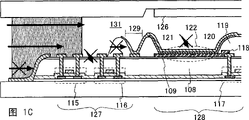
图1A至1C为根据本发明的发光装置的横截面图。基底绝缘膜101位于基片100上。其上形成有半导体层102至104。基底绝缘膜101和半导体层102至104由栅绝缘膜133覆盖。栅电极105至107位于栅绝缘膜133上,同时部分地与半导体层102至104重叠。所述栅绝缘膜133和栅电极105至107由层间绝缘膜108覆盖。绝缘膜109位于所述层间绝缘膜108上。1A to 1C are cross-sectional views of a light emitting device according to the present invention. The base insulating film 101 is on the substrate 100 . The semiconductor layers 102 to 104 are formed thereon. The base insulating film 101 and the semiconductor layers 102 to 104 are covered with a gate insulating film 133 . The gate electrodes 105 to 107 are located on the gate insulating film 133 while partially overlapping the semiconductor layers 102 to 104 . The gate insulating film 133 and the gate electrodes 105 to 107 are covered with an
基片100用于支撑薄膜晶体管和发光元件。形成基底绝缘膜101以防止对所述薄膜晶体管产生不良影响的物质扩散通过基片100。如果由所述物质引起的不良影响不是很重要,则不需要提供基底绝缘膜。薄膜晶体管包括半导体层102至104,栅绝缘膜133和栅电极105至107。所述薄膜晶体管包括形成于驱动电路部分127内的薄膜晶体管,用作驱动电路等,以及形成于像素部分128内的薄膜晶体管,用于驱动发光元件122。所述驱动电路可以以与本实施模式相同的方式与像素部分整体地形成在基片上,或者单独形成。The substrate 100 is used to support thin film transistors and light emitting elements. The base insulating film 101 is formed to prevent substances that adversely affect the thin film transistor from diffusing through the substrate 100 . If the adverse effect caused by the substance is not very important, there is no need to provide the base insulating film. The thin film transistor includes semiconductor layers 102 to 104 , a gate insulating film 133 and gate electrodes 105 to 107 . The thin film transistors include a thin film transistor formed in the
在该实施模式中,假设层间绝缘膜108由具有相对较高透水性的绝缘材料构成,例如有机绝缘膜(例如丙烯酸或聚酰亚胺)和硅氧烷。所述绝缘膜109由具有低透水性的膜形成,例如氮化硅、含有氧的氮化硅、含有氮的氧化硅和氧化硅。注意,在层间绝缘膜108和栅绝缘膜133或栅电极105至107之间可以形成由其他材料构成的绝缘膜。In this embodiment mode, it is assumed that the
通过绝缘膜109和层间绝缘膜108上形成的接触孔与半导体层102至104电连接的电极(线路)110至114形成于绝缘膜109上。薄膜晶体管115包括半导体层102,栅绝缘膜133,栅电极105,电极(线路)110和111。薄膜晶体管116包括半导体层103,栅绝缘膜133,栅电极106,电极(线路)112和113。半导体层104、栅绝缘膜133、栅电极107和电极(线路)114为薄膜晶体管117的一部分。在所述发光装置中,薄膜晶体管115和116指示了驱动电路部分127的薄膜晶体管的一部分,薄膜晶体管117是像素部分128内的薄膜晶体管中的一个。Electrodes (lines) 110 to 114 electrically connected to the semiconductor layers 102 to 104 through contact holes formed on the insulating
形成第一电极118与薄膜晶体管117的电极114接触,形成分隔壁119以覆盖第一电极的边缘。分隔壁119通常由有机绝缘膜构成,例如丙烯酸和聚酰亚胺,或由具有相对高透水性的绝缘膜构成,例如硅氧烷。分隔壁119直接与包括发光层(发光膜)120的膜接触,经分隔壁到达发光膜120的湿气被认为会导致发光元件122的可靠性下降。The
形成发光膜120与第一电极118接触。形成第二电极121以部分覆盖所述发光膜120和分隔壁119。发光元件122包括第一电极118、第二电极121、以及位于第一电极和第二电极之间的发光膜120。以矩阵形式在像素部分128内排列所述多个发光元件122。A
分隔壁119上的第一开口129环绕象素部分128的外周。第一开口129的侧壁和底面覆盖有第二电极121。当与本实施模式相同,在与像素部分128相同的基片上形成驱动电路部分127时,第一开口129位于驱动电路部分127和像素部分128之间,如图1A所示。另外,本发明当然可以应用于驱动电路没有与像素部分整合在一起的发光装置中。The
第一开口129贯穿分隔壁119。在该实施模式中,采用与电极(线路)110至114相同的材料在第一开口129的下方形成接触部分130,从而绝缘膜109较好地附着于第二电极121上。当具有低透水性的绝缘膜109与第二电极121接触时,不一定需要连接部分130。The
如果在绝缘膜109上形成将信号传输至像素部分128的线路,该线路位于由第一开口129环绕的区域内,则所述线路与第二电极121之间构成短路。为了防止短路,将信号传导至像素部分128的线路经栅电极层105至107与像素部分128的线路连接。If a line that transmits a signal to the
具有上述结构的基片100紧密地附着于具有密封材料123的相对基片124上。可以在所述相对基片124内形成凹陷部分125,其内具有干燥剂。The substrate 100 having the above structure is closely attached to the opposing substrate 124 having the sealing material 123 . A depressed portion 125 having a desiccant therein may be formed in the opposing substrate 124 .
根据该结构,发光膜120可以免于外界的湿气进入。防止湿气进入可以延长发光元件122的寿命,其增加了发光装置的可靠性。According to this structure, the
通常,具有相对较低透水性的有机材料例如紫外固化树脂用作密封材料123。然而,在该环境下,所述材料很难完全防止湿气的进入。人们认为,由于密封材料的长期使用,外界的湿气经密封膜进入发光元件。如果密封材料没有很好地粘附于基片、相对基片等,则湿气可能通过粘接较差的地方进入。因此采用密封材料很难完全阻止外界的湿气进入。从外界经密封材料进入发光膜120的湿气被认为是进行性缺陷的原因之一。湿气从外界经过几个途径进入发光膜120。内部环境131、分隔壁119和层间绝缘膜108被认为是湿气从密封材料123进入发光膜120的主要途径。图1A和1C中的箭头示意性地显示了湿气渗透的路径。Generally, an organic material having relatively low water permeability such as an ultraviolet curing resin is used as the sealing material 123 . However, in this environment, it is difficult for the material to completely prevent the ingress of moisture. It is considered that moisture from the outside enters the light-emitting element through the sealing film due to long-term use of the sealing material. If the encapsulant does not adhere well to the substrate, opposing substrate, etc., moisture may enter through the poor bond. Therefore, it is difficult to completely prevent external moisture from entering by using a sealing material. Moisture entering the
当干燥剂126位于相对基片上时,分散在内部环境131中的湿气在某种程度上被干燥剂吸收,没有被干燥剂吸收的湿气残留在内部环境中或者渗透(或再次渗透)进入分隔壁119。由于第二电极121具有低的透水性,残留在内部环境131中的湿气不能到达发光膜120。优选地,第二电极121上没有小孔。关于从密封材料123和内部环境131进入分隔壁119的湿气,覆盖第一开口129的侧壁和底面的第二电极121明确存在于湿气达到发光膜120的路径上。由于第二电极121不允许湿气通过,湿气不能到达发光膜120。而且由于绝缘膜109的存在,进入层间绝缘膜108的湿气不能达到发光膜120。因此,在该实施模式中,湿气从外界环境到达发光膜120的渗透路径被切断了,因此可以避免外界湿气的不良影响。注意,在图1A至1C中,由十字表示的箭头表示了湿气被低透水性材料阻断以免进一步进入发光膜一侧的情况。When the
如图1A至1C所示,优选其中层间绝缘膜108的边缘被具有低透水性的膜134覆盖的结构,以减少湿气经层间绝缘膜108的边缘渗透的量。当具有低透水性的膜134由与电极(线路)110至114、接触部分130等相同的材料构成时,膜134可以用作导线。As shown in FIGS. 1A to 1C , a structure in which the edges of the
图1B描述了一种结构,其中在图1A的结构上另外形成有直至下一层的第二开口132。形成第二开口132从而在厚度方向上贯穿分隔壁119。第二开口132环绕第一开口129的外周,并阻止从密封材料进入分隔壁119的湿气直接经分隔壁119进入第一开口129。其减少了到达第一开口129的湿气量,这使发光元件122的可靠性得到改善。可以省略分隔壁119的一部分,如图1C所示。FIG. 1B depicts a structure in which a
然而,图6显示了作为比较例的常规发光装置的横截面图。注意,在该情况下,图6中用于各个组件部分的材料与图1A中的相应部分相同。在图6中,外界的湿气首先经层间绝缘膜200和密封材料201渗透。经层间绝缘膜200渗透的湿气进一步进入分隔壁202,然后到达发光膜203。经密封材料201渗透的湿气分散在内部环境204中。内部环境204中的湿气有一部分被干燥剂205吸收,一部分留在内部环境204中,一部分渗透进入分隔壁202。进入分隔壁202的湿气到达发光膜203。到达发光膜203的湿气损坏发光膜203,其导致发光元件206的可靠性下降。However, FIG. 6 shows a cross-sectional view of a conventional light emitting device as a comparative example. Note that in this case, the materials used for the respective component parts in FIG. 6 are the same as the corresponding parts in FIG. 1A. In FIG. 6 , moisture from the outside first penetrates through the interlayer insulating film 200 and the sealing material 201 . The moisture permeated through the interlayer insulating film 200 further enters the partition wall 202 and then reaches the light emitting film 203 . Moisture that has penetrated through the sealing material 201 is dispersed in the internal environment 204 . A part of the moisture in the internal environment 204 is absorbed by the desiccant 205 , a part remains in the internal environment 204 , and a part penetrates into the partition wall 202 . Moisture entering the partition wall 202 reaches the light emitting film 203 . Moisture reaching the light emitting film 203 damages the light emitting film 203 , which leads to a decrease in the reliability of the light emitting element 206 .
实施模式2Implementation Mode 2
在本实施模式中将参考图2A和2B描述本发明的另一实施模式。注意,对与图1A至1C中相同的部分有可能不作进一步的解释。Another embodiment mode of the present invention will be described in this embodiment mode with reference to FIGS. 2A and 2B. Note that further explanation may not be given for the same parts as in FIGS. 1A to 1C .
图2B显示的例子中层间绝缘膜300由例如氧化硅、氮化硅、含氮的氧化硅和含氧的氮化硅的材料构成。层间绝缘膜300可以包括单层或层压层。由于这些材料具有低的透水性,当它们暴露于外界空气时,湿气很难渗透,因此湿气很难渗透层间绝缘膜300,该绝缘膜的边缘没有用如图1A所示的具有低透水性的膜134覆盖。另外,也可以不提供对应于如图1A所示的绝缘膜109的结构。注意,其它结构同实施模式1中,不再进一步地解释。FIG. 2B shows an example in which interlayer insulating
图2A显示了作为比较例的常规结构。尽管可以忽略透过层间绝缘膜300的湿气,但是渗透通过密封材料301的湿气进入内部环境302和分隔壁303中。进入分隔壁303的湿气到达发光膜304,从而损坏发光元件307。Fig. 2A shows a conventional structure as a comparative example. Although the moisture penetrating through the
图2B为应用本发明的发光装置的横截面图。在图2B中,分隔壁303上形成直至下一层的开口305,开口305的内表面和底面由第二电极306覆盖。由于第二电极306具有低的透水性,渗透通过分隔壁303的湿气不能到达发光膜304。另外,第二电极121上没有小孔。根据本发明,可以阻断损坏发光膜304的湿气,从而防止发光膜304的损坏。Fig. 2B is a cross-sectional view of a light emitting device to which the present invention is applied. In FIG. 2B , an opening 305 to the next layer is formed in the
注意,层间绝缘膜300和栅电极或栅绝缘膜之间可以形成由另一材料构成的绝缘膜。然而,在此情况下,所述具有低透水性的绝缘膜必须类似于层间绝缘膜300。Note that an insulating film made of another material may be formed between the interlayer insulating
注意,接触部分308具有与图1A中的接触部分130相同的功能,也可以象接触部分130一样,不提供接触部分308。Note that the contact portion 308 has the same function as the contact portion 130 in FIG. 1A , and like the contact portion 130 , the contact portion 308 may not be provided.
实施模式3Implementation Mode 3
参考图3描述本发明的另一实施模式。有可能对与图1A至1C中相同的部分不作进一步的解释。Another embodiment mode of the present invention is described with reference to FIG. 3 . It is possible not to give further explanation on the same parts as in Figs. 1A to 1C.
在该实施模式中,描述的例子中线路401至405和像素电极(第一电极)406位于不同层。在该实施模式中,绝缘膜408位于第一层间绝缘膜407上。第一层间绝缘膜407假设由例如丙烯酸和聚酰亚胺的有机绝缘膜构成,或由具有相对较高透水性的绝缘膜构成,例如硅氧烷。另外,绝缘膜408由具有低透水性的材料构成,例如氮化硅、含氧的氮化硅、含氮的氧化硅和氧化硅。In this embodiment mode, an example is described in which the lines 401 to 405 and the pixel electrode (first electrode) 406 are located on different layers. In this embodiment mode, the insulating film 408 is located on the first interlayer insulating film 407 . The first interlayer insulating film 407 is assumed to be composed of an organic insulating film such as acrylic and polyimide, or an insulating film having relatively high water permeability such as siloxane. In addition, the insulating film 408 is made of a material having low water permeability, such as silicon nitride, silicon nitride containing oxygen, silicon oxide containing nitrogen, and silicon oxide.
注意,可以在第一层间绝缘膜407和栅电极或栅绝缘膜之间进一步提供一个或多个绝缘膜。Note that one or more insulating films may be further provided between the first interlayer insulating film 407 and the gate electrode or gate insulating film.
电极(线路)401至405位于绝缘膜408上,通过位于绝缘膜408和第一层间绝缘膜407上的接触孔与半导体层409至411电接触。Electrodes (wiring) 401 to 405 are located on insulating film 408 and are in electrical contact with semiconductor layers 409 to 411 through contact holes located on insulating film 408 and first interlayer insulating film 407 .
绝缘膜408和电极(线路)401至405由第二层间绝缘膜412覆盖。在第二层间绝缘膜412上形成有接触孔和第一开口414,接触孔直至像素部分413的薄膜晶体管的电极405,第一开口414环绕像素部分的外周。第一开口414贯穿第二层间绝缘膜。当如本实施模式所示,驱动电路部分425和像素部分413位于同一基片上方时,第一开口414位于驱动电路部分425和像素部分413之间。本发明当然适合于驱动电路没有与像素部分整体地位于同一基片上的发光装置。The insulating film 408 and the electrodes (wiring) 401 to 405 are covered with a second interlayer insulating film 412 . A contact hole up to the electrode 405 of the thin film transistor of the pixel portion 413 and a first opening 414 surrounding the periphery of the pixel portion are formed on the second interlayer insulating film 412 . The first opening 414 penetrates through the second interlayer insulating film. When the driving circuit portion 425 and the pixel portion 413 are located over the same substrate as shown in this embodiment mode, the first opening 414 is located between the driving circuit portion 425 and the pixel portion 413 . The present invention is of course suitable for light-emitting devices in which the driving circuit is not integrally located on the same substrate as the pixel portion.
发光元件416的第一电极406位于第二层间绝缘膜412上,从而第一电极经第二层间绝缘膜412上形成的接触孔与薄膜晶体管的电极405电连接。The first electrode 406 of the light emitting element 416 is located on the second interlayer insulating film 412 , so that the first electrode is electrically connected to the electrode 405 of the thin film transistor through a contact hole formed on the second interlayer insulating film 412 .
分隔壁417位于第二层间绝缘膜412上,从而覆盖接触孔和第一电极406的边缘。第二开口418形成于分隔壁417上,其位置对应于位于第二层间绝缘膜412上的第一开口414。换言之,第一开口414与第二开口418重叠。第二开口418的底面位于第一开口414内,并直至绝缘膜408。与第一开口相同,第二开口418环绕像素部分413的外周。The partition wall 417 is located on the second interlayer insulating film 412 so as to cover the contact hole and the edge of the first electrode 406 . The second opening 418 is formed on the partition wall 417 at a position corresponding to the first opening 414 on the second interlayer insulating film 412 . In other words, the first opening 414 overlaps the second opening 418 . The bottom surface of the second opening 418 is located in the first opening 414 and extends to the insulating film 408 . Like the first opening, the second opening 418 surrounds the periphery of the pixel portion 413 .
优选地,面对第一电极406的分隔壁417的边缘具有一曲率,并具有锥形形状,所述曲率不断变化。形成发光膜423以覆盖分隔壁417的一部分和第一电极406。形成第二电极419从而覆盖分隔壁417的一部分和发光膜423。第二电极419覆盖位于分隔壁417上的第二开口418的内表面和底面。Preferably, the edge of the partition wall 417 facing the first electrode 406 has a curvature and has a tapered shape, said curvature constantly changing. A light emitting film 423 is formed to cover a part of the partition wall 417 and the first electrode 406 . The second electrode 419 is formed so as to cover a part of the partition wall 417 and the light emitting film 423 . The second electrode 419 covers the inner surface and the bottom surface of the second opening 418 on the partition wall 417 .
采用有机绝缘材料例如丙烯酸和聚酰亚胺、硅氧烷等,作为构成第二层间绝缘膜和分隔壁的材料。公知的是,这些材料具有相对较高的透水性。因此,渗透通过密封膜的外界湿气被认为经第二层间绝缘膜和分隔壁到达发光膜423。然而,在具有本发明结构的发光装置中,湿气从外界到达发光膜423的路径被第二电极419切断了,第二电极419覆盖形成于第一层间绝缘膜407的第一开口414和形成于分隔壁417上的第二开口418的侧面和底面。An organic insulating material such as acrylic and polyimide, siloxane, etc. is used as a material constituting the second interlayer insulating film and the partition wall. These materials are known to have relatively high water permeability. Therefore, external moisture permeating through the sealing film is considered to reach the light emitting film 423 through the second interlayer insulating film and the partition wall. However, in the light-emitting device having the structure of the present invention, the path of moisture from the outside to the light-emitting film 423 is cut off by the second electrode 419 covering the first opening 414 and the first opening 414 formed in the first interlayer insulating film 407. Sides and bottoms of the second opening 418 formed on the partition wall 417 .
其上形成有元件的基片420牢固地附着于具有密封材料421的相对基片422上,从而构成了一发光装置。A substrate 420 on which elements are formed is firmly attached to an opposite substrate 422 having a sealing material 421, thereby constituting a light emitting device.
根据上述结构,当发光元件的第一电极406和线路401至405位于不同层的情况下,由来自外界的湿气而导致的发光膜423的损坏将会减少。也就是说,具有上述结构的发光装置包括两个层间绝缘膜。因此发光元件416的寿命可以延长,从而提高了发光装置的可靠性。也就是说,本发明的发光装置包括的结构切断了湿气从外界环境经密封材料421渗透的路径。According to the above structure, when the first electrode 406 of the light emitting element and the wires 401 to 405 are located in different layers, damage to the light emitting film 423 caused by moisture from the outside will be reduced. That is, the light emitting device having the above structure includes two interlayer insulating films. Therefore, the lifetime of the light emitting element 416 can be extended, thereby improving the reliability of the light emitting device. That is to say, the structure included in the light-emitting device of the present invention cuts off the path for moisture to permeate from the external environment through the sealing material 421 .
对湿气的渗透路径进行简单描述。首先,由于绝缘膜408的存在,渗透通过第一层间绝缘膜407的湿气不能进入发光膜423侧。同样,当第一层间绝缘膜407的外周边缘部分由具有低透水性的膜424覆盖时,如图3所示,可以有效减少进入第一层间绝缘膜407的绝对湿气量。Briefly describe the permeation path of moisture. First, due to the presence of the insulating film 408, moisture permeating through the first interlayer insulating film 407 cannot enter the light emitting film 423 side. Also, when the outer peripheral edge portion of first interlayer insulating film 407 is covered with film 424 having low water permeability, as shown in FIG. 3 , the absolute amount of moisture entering first interlayer insulating film 407 can be effectively reduced.
接下来,由于第一开口414、第二开口418和覆盖第二开口侧面和底面的第二电极419,渗透通过密封材料421进入第二层间绝缘膜412和分隔壁417的湿气很难再进入发光膜423侧。Next, due to the first opening 414, the second opening 418, and the second electrode 419 covering the side and bottom surfaces of the second opening, the moisture that permeates through the sealing material 421 and enters the second interlayer insulating film 412 and the partition wall 417 is difficult to regenerate. Enter the luminescent film 423 side.
形成于第二开口418底面上的第二电极419与绝缘膜408接触,并阻止湿气的渗透。The second electrode 419 formed on the bottom surface of the second opening 418 is in contact with the insulating film 408 and prevents the penetration of moisture.
尽管位于第二开口418底面上的第二电极419与绝缘膜408接触,但是接触部分可以由与线路401至405相同的材料构成,其结构类似于实施模式1中所述的结构(图1A中的接触部分130)。Although the second electrode 419 located on the bottom surface of the second opening 418 is in contact with the insulating film 408, the contact portion may be made of the same material as the wiring lines 401 to 405, and its structure is similar to that described in Embodiment Mode 1 (in FIG. 1A contact portion 130).
实施模式4Implementation Mode 4
参照图4A和4B描述本发明的另一实施模式。注意,对与图1A至1C和图3中相同的部分不作进一步解释。Another embodiment mode of the present invention is described with reference to FIGS. 4A and 4B. Note that the same parts as those in FIGS. 1A to 1C and FIG. 3 will not be further explained.
在该实施模式中,解释的例子中线路501至505和像素电极(第一电极)506形成在不同层中。该实施模式显示的例子中第一层间绝缘膜507由氧化硅、氮化硅、含氮的氧化硅和含氧的氮化硅等中的任意一个构成。第一层间绝缘膜507可以包括单层或层压层。由于这些材料具有低的透水性,如果第一层间绝缘膜507的外周部分暴露于外周空气,湿气很难渗透进入。因此,没有用例如图3所示的具有低透水性的膜覆盖第一层间绝缘膜的边缘,第一层间绝缘膜507也很难被湿气渗透。同样,可以不提供对应于图3所示的绝缘膜408的结构。其它结构同实施模式3。In this embodiment mode, the example explained is that the
图4A为常规发光装置的横截面图。在常规结构中,从外界渗透通过密封材料508的湿气通过迁移通过内部环境509、分隔壁510和第二层间绝缘膜511而经分隔壁510到达发光膜512。其导致发光膜512的损坏。而在本实施模式中,作为前提,第一层间绝缘膜507由具有低透水性的材料构成,因此,可以忽略渗透通过第一层间绝缘膜507的湿气。FIG. 4A is a cross-sectional view of a conventional light emitting device. In a conventional structure, moisture permeating through the sealing
另一方面,图4B为根据本发明的发光装置的横截面图。在图4B中,第一开口513和第二开口514分别形成于第二层间绝缘膜511和由具有高透水性的材料构成的分隔壁510中。第二开口514的侧面和底面由发光元件516的第二电极515覆盖。第一开口513和第二开口514均环绕像素部分,从而切断了外界湿气经第二层间绝缘膜511和分隔壁510渗透到达发光膜512的路径。On the other hand, FIG. 4B is a cross-sectional view of a light emitting device according to the present invention. In FIG. 4B , a
根据该结构,可以阻止外界湿气的进入。由于可以降低发光膜512的损坏,发光元件516的寿命可以延长,从而提高了发光装置的可靠性。According to this structure, entry of external moisture can be blocked. Since the damage of the light-emitting
实施模式5Implementation Mode 5
参照图5A和5B描述本发明的另一实施模式。注意,对与图1A至1C和图3中相同的部分不作进一步解释。Another embodiment mode of the present invention is described with reference to FIGS. 5A and 5B. Note that the same parts as those in FIGS. 1A to 1C and FIG. 3 will not be further explained.
该实施模式具有类似于图1A至1C和图3的结构。参照图5A和5B以及图7A和7B对层间绝缘膜600上没有形成具有低透水性的绝缘膜的结构进行描述。This embodiment mode has a structure similar to FIGS. 1A to 1C and FIG. 3 . A structure in which no insulating film having low water permeability is formed on the
在图5A的结构中,发光膜607形成于层间绝缘膜600上方。开口602位于分隔壁601中并环绕像素部分603,开口602的侧面和底面覆盖有第二电极605。因此可以防止湿气的进入。In the structure of FIG. 5A , a
在图5B的结构中,开口610形成于导线608和驱动电路部分609之间的层间绝缘膜600、栅绝缘膜、基底绝缘膜等上,开口610的侧面和底面覆盖有具有低透水性的膜611。进一步地,发光元件604的第二电极605的边缘与具有低透水性的膜611接触,从而防止从外界渗透通过密封材料606的湿气进入层间绝缘膜600和分隔壁601。注意,当构成具有低透水性的膜611的材料与像素部分603或驱动电路部分609内形成的薄膜晶体管的线路或电极612至616的材料相同并一次加工而成时,可以减少步骤。In the structure of FIG. 5B, the
注意,在该实施模式中,由于层间绝缘膜600上形成的开口610位于接收外界信号的驱动电路部分之外,因此,在如图15所示的接收外界信号的导线部分(图15中的(a)区域)内可以不提供开口610。然而,该结构仍能改善抗湿气的可靠性。Note that in this implementation mode, since the
在图7A的结构中,发光膜704形成于层间绝缘膜701上方。开口位于分隔壁703中并环绕像素部分,所述开口的侧面和底面覆盖有第二电极。因此可以防止湿气的进入。In the structure of FIG. 7A , a
在所述结构中,开口707形成于驱动电路部分705的外周部分内的第一层间绝缘膜702、栅绝缘膜、基底绝缘膜等上,开口707的侧面和底面覆盖有具有低透水性的膜708,其方式如图7B所示的实施模式。进一步地,发光元件709的第二电极710的边缘与具有低透水性的膜708接触,从而防止从外界渗透通过密封材料700的湿气进入第一层间绝缘膜702、第二层间绝缘膜701和分隔壁703。优选地,构成具有低透水性的膜708的材料与像素部分711或驱动电路部分705内形成的薄膜晶体管的线路或电极712至716的材料相同并同时形成,从而不增加步骤。In the structure, the opening 707 is formed on the first
注意,尽管本文中开口707形成于第一层间绝缘膜702上以抑制湿气进入第一层间绝缘膜,但是在导线部分内,在第一层间绝缘膜702的上方和下方具有密集的线路,由于不能移去第一层间绝缘膜702以防止上部和下部线路之间发生短路,因而所述开口不能形成于导线部分(图15所示的(a)区域)。因此,开口707不能完全环绕像素部分711。然而,由于可以在至少其它部分上形成开口,因此可以预期到本发明的效果。Note that although the openings 707 are formed here on the first
实施模式6Implementation Mode 6
本实施模式将参照图14描述对应于本发明一个模式的发光装置面板的外视图的例子。图14为面板的顶视图,其中形成于基片上方的晶体管和发光元件由密封材料密封在相对基片4006和基片之间。图14包括了实施模式1至5的任一结构。This embodiment mode will describe an example of an external view of a light emitting device panel corresponding to one mode of the present invention with reference to FIG. 14 . FIG. 14 is a top view of a panel in which transistors and light emitting elements formed above the substrate are sealed between the opposing
密封材料4005环绕位于基片4001上方的像素部分4002、信号线驱动电路4003和扫描线驱动电路4004。相对基片4006位于像素部分4002、信号线驱动电路4003和扫描线驱动电路4004的上方。因此,像素部分4002、信号线驱动电路4003和扫描线驱动电路4004以及装填物由基片4001、密封材料4005和相对基片4006密封。信号线驱动电路4003、扫描线驱动电路4004和像素部分4002之间形成有开口4000,其中开口的侧面和底面由第二电极覆盖。The sealing
位于基片4001上方的像素部分4002、信号线驱动电路4003和扫描线驱动电路4004包括多个薄膜晶体管。The
一个导线对应于将信号或电压提供至像素部分4002、信号线驱动电路4003和扫描线驱动电路4004的线路。所述导线联接于连接终端,所述连接终端经各向异性导电膜与软性印刷电路(FPC)4018的终端连接。One wire corresponds to a line that supplies a signal or voltage to the
作为装填物,可以采用例如氮气和氩气的惰性气体、紫外固化粘接剂和热固化粘接剂。另外,可以采用聚氯乙稀、丙烯酸、聚酰亚胺、环氧树脂、硅树脂、聚乙烯醇缩丁醛或乙烯乙酸乙烯酯。As the filler, an inert gas such as nitrogen and argon, an ultraviolet curing adhesive, and a heat curing adhesive can be used. In addition, polyvinyl chloride, acrylic, polyimide, epoxy, silicone, polyvinyl butyral, or ethylene vinyl acetate may be used.
图15显示的情况中开口4000位于信号线驱动电路4003和扫描线驱动电路4004之外,如实施模式5所示。如实施模式5中所示,如果开口4000位于接收外界信号的导线部分(图15的(a)区域)中,则在所述结构中线路短路。尽管开口4000不能完全环绕像素部分4002,但本发明在像素部分之外的部分仍然是有效的。In the case shown in FIG. 15 , the
注意,本发明的显示装置包括其上形成有发光元件的像素部分的面板,以及有IC安装在此类型面板上的模块。Note that the display device of the present invention includes a panel on which a pixel portion of a light emitting element is formed, and a module having an IC mounted on this type of panel.
实施模式7Implementation Mode 7
安装有类似于实施模式6所示的模块的本发明的各种电子设备包括例如摄像机和数码相机的照相机、目镜式显示器(戴在头上的显示器)、导航系统、声音复制装置(例如汽车声频组件系统)、个人计算机、游戏机、便携式信息终端(例如掌上电脑、手机、便携式游戏机和电子书籍)、具有记录介质的图像复制装置(典型地,可以复制例如数字化通用光盘(DVD)的记录介质并显示其图像的装置),等等。这些电子设备的具体例子参见图16A至16E。Various electronic devices of the present invention equipped with modules similar to those shown in Embodiment Mode 6 include cameras such as video cameras and digital cameras, eyepiece displays (displays worn on the head), navigation systems, sound reproduction devices such as car audio component systems), personal computers, game machines, portable information terminals (such as handheld computers, mobile phones, portable game machines, and electronic books), image reproduction devices with recording media (typically, recordings such as Digital Versatile Discs (DVD) can be reproduced medium and display its image), etc. Specific examples of these electronic devices are shown in Figures 16A to 16E.
图16A为例如电视的发光装置,包括外壳2001,显示器部分2003,扬声器部分2004等。在本发明的发光装置中,控制了显示器部分2003的发光元件的损坏,从而提高了可靠性。为了增加对比度,像素部分可以包括起偏振片或圆起偏振片。例如,优选通过顺序层压1/4λ片、1/2λ片和起偏振片,而在密封基片上形成膜。另外,可以在起偏振片上层压抗反射膜。Fig. 16A is a lighting device such as a television, including a housing 2001, a display part 2003, a speaker part 2004 and the like. In the light emitting device of the present invention, damage to the light emitting elements of the display portion 2003 is controlled, thereby improving reliability. In order to increase contrast, the pixel portion may include a polarizing plate or a circular polarizing plate. For example, it is preferable to form a film on a sealing substrate by sequentially laminating a 1/4λ plate, a 1/2λ plate and a polarizing plate. In addition, an antireflection film may be laminated on the polarizing plate.
图16B显示了一手机,其包括主体2101、外壳2102、显示器部分2103、音频输入部分2104、音频输出部分2105、操作键2106、天线2108等。根据本发明,该手机的显示器部分2103的发光元件的损坏被抑制,从而提高了可靠性。FIG. 16B shows a mobile phone including a
图16C显示了笔记本电脑,包括主体2201、外壳2202、显示器部分2203、键盘2204、外部连接端口2205、鼠标2206等。根据本发明,该笔记本电脑的显示器部分2203的发光元件的损坏被抑制,从而提高了可靠性。FIG. 16C shows a notebook computer including a
图16D显示了掌上电脑,包括主体2301、显示器部分2302、开关2303、操作键2304、红外端口2305等。根据本发明,该掌上电脑的显示器部分2302的发光元件的损坏被抑制,从而提高了可靠性。FIG. 16D shows a handheld computer, including a
图16E显示了便携式游戏机,包括包括主体2401、显示器部分2402、扬声器部分2403、操作键2404、记录介质插入部分2405等。根据本发明,该导向器的显示器部分2402的发光元件的损坏被抑制,从而提高了可靠性。FIG. 16E shows a portable game machine including a main body 2401, a display portion 2402, a speaker portion 2403, operation keys 2404, a recording medium insertion portion 2405, and the like. According to the present invention, damage to the light emitting elements of the display portion 2402 of the director is suppressed, thereby improving reliability.
如上所述,本发明的应用范围非常广泛,本发明可以应用于各个领域的电子设备。As described above, the application range of the present invention is very wide, and the present invention can be applied to electronic devices in various fields.
实施例1Example 1
参照图8A至8D和图9A至9C描述生产本发明的发光装置的方法。A method of producing the light emitting device of the present invention is described with reference to FIGS. 8A to 8D and FIGS. 9A to 9C.
在基片800上形成绝缘层801之后,在绝缘层801上形成半导体层(图8A)。After the insulating layer 801 is formed on the substrate 800, a semiconductor layer is formed on the insulating layer 801 (FIG. 8A).
作为基片800的材料,可以选用透光玻璃、石英、塑料(聚酰亚胺、丙烯酸、聚对苯二甲酸乙二醇酯、聚碳酸酯、聚丙烯酸酯、聚醚砜)等。如果需要,可以对这些基片用CMP等进行抛光。本实施例采用了玻璃基片。As the material of the substrate 800, light-transmitting glass, quartz, plastic (polyimide, acrylic, polyethylene terephthalate, polycarbonate, polyacrylate, polyethersulfone) and the like can be selected. These substrates may be polished by CMP or the like, if necessary. In this embodiment, a glass substrate is used.
提供绝缘层801以防止元素,例如基片800中所含有的碱金属和碱土金属进入半导体层从而对半导体膜的特性产生不良影响。作为绝缘层801的材料,可以采用氧化硅、氮化硅、含有氮的氧化硅和含有氧的氮化硅等。绝缘层可以为单层或层压层。如果碱金属和碱土金属的扩散不重要,则不需要形成绝缘膜801。The insulating layer 801 is provided to prevent elements such as alkali metals and alkaline earth metals contained in the substrate 800 from entering the semiconductor layer to adversely affect the characteristics of the semiconductor film. As the material of the insulating layer 801, silicon oxide, silicon nitride, silicon oxide containing nitrogen, silicon nitride containing oxygen, or the like can be used. The insulating layer can be a single layer or a laminated layer. If diffusion of alkali metals and alkaline earth metals is not important, it is not necessary to form insulating film 801 .
在该实施例中,通过激光束使无定形硅膜晶体化,从而形成半导体层。无定形硅膜在绝缘层801上的厚度为25至100nm(优选,30至60nm)。就制作方法而言,可以采用公知的方法,例如喷溅、减压CVD和等离子CVD。之后,将无定形硅膜在500℃下热处理一小时,以脱氢。In this embodiment, an amorphous silicon film is crystallized by a laser beam, thereby forming a semiconductor layer. The thickness of the amorphous silicon film on the insulating layer 801 is 25 to 100 nm (preferably, 30 to 60 nm). As the fabrication method, known methods such as sputtering, reduced-pressure CVD, and plasma CVD can be employed. After that, the amorphous silicon film was heat-treated at 500° C. for one hour to dehydrogenate.
接下来,采用激光照射设备对无定形硅膜进行晶体化从而形成晶体硅膜。在该实施例中采用准分子激光器进行激光晶体化。采用光学系统将所述准分子激光器振荡产生的激光处理成线性束光,从而照射无定形硅膜,由此,得到晶体硅膜并用作半导体层。Next, the amorphous silicon film is crystallized using a laser irradiation device to form a crystalline silicon film. Laser crystallization is performed using an excimer laser in this example. The laser light oscillated by the excimer laser is processed into a linear beam using an optical system to irradiate the amorphous silicon film, whereby a crystalline silicon film is obtained and used as a semiconductor layer.
作为对无定形硅膜进行晶体化的其它方法,其中一种是仅仅进行热处理以晶体化,另一种是采用促进晶体化的催化元素进行热处理从而晶体化。就促进晶体化的元素而言,可以引用镍、钢、钯、锡、铅、钴、铂、铜、金等。与仅仅通过热处理进行晶体化的情况相比,采用促进晶体化的元素而进行晶体化的温度更低、时间更短,从而很难损坏玻璃基片等。当仅仅通过热处理进行晶体化时,必须采用耐热石英作为基片800。As other methods of crystallizing an amorphous silicon film, one is to crystallize by heat treatment only, and the other is to crystallize by heat treatment using a catalyst element that promotes crystallization. As elements promoting crystallization, nickel, steel, palladium, tin, lead, cobalt, platinum, copper, gold and the like can be cited. Compared with the case of crystallization by only heat treatment, the crystallization is performed at a lower temperature and shorter time using an element that promotes crystallization, so that it is difficult to damage the glass substrate or the like. When crystallization is performed only by heat treatment, it is necessary to use heat-resistant quartz as the substrate 800 .
如果需要的话,在半导体层中加入少量的杂质(即所谓的沟道掺杂)以控制阈值。为了得到预定的阈值,通过离子掺杂等在半导体层中加入赋予n型或p型导电性的杂质(例如磷和硼)。If necessary, small amounts of impurities (so-called channel doping) are added to the semiconductor layer to control the threshold. In order to obtain a predetermined threshold, impurities imparting n-type or p-type conductivity (for example, phosphorus and boron) are added to the semiconductor layer by ion doping or the like.
之后,如图8A所示将半导体层加工成预定形状,从而得到岛状半导体层802至804。具体而言,所述半导体层按照以下方式形成图案。在半导体层上施加光刻胶,在预定图案下暴露并焙烧所述半导体层,在半导体层上形成一抗蚀剂掩膜,采用所述掩膜蚀刻所述半导体层。After that, the semiconductor layer is processed into a predetermined shape as shown in FIG. 8A , thereby obtaining island-shaped semiconductor layers 802 to 804 . Specifically, the semiconductor layer was patterned as follows. applying a photoresist on the semiconductor layer, exposing and firing the semiconductor layer under a predetermined pattern, forming a resist mask on the semiconductor layer, and etching the semiconductor layer by using the mask.
形成栅绝缘膜805以覆盖岛状半导体层802至804。就栅绝缘膜805而言,通过等离子CVD或喷溅形成含有硅的绝缘膜从而使厚度为40至150nm。A gate insulating film 805 is formed to cover the island-shaped semiconductor layers 802 to 804 . As for the gate insulating film 805, an insulating film containing silicon is formed by plasma CVD or sputtering so as to have a thickness of 40 to 150 nm.
在栅绝缘膜805上形成栅电极806至808。栅电极806至808可以由选自Ta、W、Ti、Mo、Al、Cu、Cr、Nd的元素、以及含有上述元素作为其主成分的合金材料或复合材料构成。另一选择,可以使用以掺有杂质元素例如磷的多晶硅为代表的半导体膜。或者,可以使AgPdCu合金。Gate electrodes 806 to 808 are formed on the gate insulating film 805 . The gate electrodes 806 to 808 can be composed of elements selected from Ta, W, Ti, Mo, Al, Cu, Cr, Nd, and alloy materials or composite materials containing the above elements as their main components. Alternatively, a semiconductor film typified by polysilicon doped with an impurity element such as phosphorus may be used. Alternatively, AgPdCu alloys can be made.
尽管形成的栅电极806至808具有单层,它们也可以包括具有两层或多层的层压层,例如钨为下层,而钼为上层。在形成具有层压结构的栅电极时,可以使用前述的材料。可以任意选择这些材料的组合。Although the gate electrodes 806 to 808 are formed to have a single layer, they may also include laminated layers having two or more layers, such as tungsten as the lower layer and molybdenum as the upper layer. In forming the gate electrode having a laminated structure, the aforementioned materials can be used. Combinations of these materials can be selected arbitrarily.
采用由光刻胶构成的掩膜蚀刻栅电极806至808。The gate electrodes 806 to 808 are etched using a mask made of photoresist.
接下来,在岛状半导体层802至804中加入高浓度杂质,与此同时利用栅电极806至808作为掩膜。因此,形成了包括半导体层802至804,栅绝缘膜805和栅电极806至808的薄膜晶体管。Next, high-concentration impurities are added to the island-shaped semiconductor layers 802 to 804 while using the gate electrodes 806 to 808 as masks. Thus, a thin film transistor including the semiconductor layers 802 to 804, the gate insulating film 805, and the gate electrodes 806 to 808 is formed.
对生产薄膜晶体管的步骤并没有特别的限制,可以任意改变从而得到具有预定结构的晶体管。There is no particular limitation on the steps of producing a thin film transistor, and can be changed arbitrarily to obtain a transistor with a predetermined structure.
尽管本实施例采用的顶浇式薄膜晶体管使用了经激光晶体化的晶体硅膜,但是也可以采用底浇式薄膜晶体管作为像素部分,其中底浇式薄膜晶体管采用无定形半导体膜。除了硅之外,锗化硅可以用作无定形半导体膜。当采用锗化硅时,锗的浓度优选为0.01至4.5原子%。Although the laser-crystallized crystalline silicon film is used for the top-cast TFT used in this embodiment, it is also possible to use a bottom-cast TFT using an amorphous semiconductor film as the pixel portion. In addition to silicon, silicon germanium can be used as the amorphous semiconductor film. When silicon germanium is used, the concentration of germanium is preferably 0.01 to 4.5 atomic %.
另一选择,可以采用微晶体半导体膜(即半无定形半导体),其中无定形半导体膜上可以观察到0.5至20nm的晶粒。其中可以观察到0.5至20nm的晶粒的细小晶体也称为所谓的微晶体(μc)。Alternatively, a microcrystalline semiconductor film (ie, a semi-amorphous semiconductor) in which crystal grains of 0.5 to 20 nm can be observed can be used. Fine crystals in which crystal grains of 0.5 to 20 nm can be observed are also called so-called microcrystals (μc).
作为半无定形半导体的所述半无定形硅(也可以用SAS表示)可以通过硅化物气体的辉光放电分解形成。SiH4为代表性的硅化物气体,除了SiH4之外,也可以使用Si2H6,SiH2Cl2,SiHCl3,SiCl4,SiF4等。用氢气或氢气和一种或多种稀少气体元素的混合物稀释所述硅化物气体可以很容易地形成SAS,所述稀少气体元素选自氦、氩、氪和氖。稀释比可以为1∶10至1∶1000。可以在0.1Pa至133Pa的压力下反应生成辉光放电分解的基膜。可以将辉光放电的高频电源设置为1至120MHz,优选为13至60MHz。可以将基片的加热温度设置为300℃或更低,优选100至250℃。The semi-amorphous silicon (also denoted by SAS) which is a semi-amorphous semiconductor can be formed by glow discharge decomposition of silicide gas. SiH 4 is a representative silicide gas, and besides SiH 4 , Si 2 H 6 , SiH 2 Cl 2 , SiHCl 3 , SiCl 4 , SiF 4 and the like can also be used. SAS can be readily formed by diluting the silicide gas with hydrogen or a mixture of hydrogen and one or more rare gas elements selected from the group consisting of helium, argon, krypton and neon. The dilution ratio can be from 1:10 to 1:1000. It can react under the pressure of 0.1Pa to 133Pa to form the base film decomposed by glow discharge. The high-frequency power supply for glow discharge can be set at 1 to 120 MHz, preferably 13 to 60 MHz. The heating temperature of the substrate can be set to 300°C or lower, preferably 100 to 250°C.
由此形成的SAS的拉曼光谱偏移至比520cm-1更低的波长数。通过X线衍射可以在SAS中观察到衍射峰(111)至(220),这些衍射峰被认为来源于硅晶格。进一步地,在SAS中加入至少1原子%的氢或卤素,作为侧链键(dangling bonds)的中和剂。至于膜中含有的杂质元素,作为大气组成物的杂质例如氧、氮或碳的每种的浓度设为1×1020cm-1或更低。尤其是,氧浓度设为5×1019cm-3或更低;更优选地,1×1019cm-3或更低。采用SAS的TFT的电场效应迁移率μ为1至10cm2/Vsec。可以通过激光束对SAS进一步地晶体化。The Raman spectrum of the resulting SAS is shifted to lower wavelength numbers than 520 cm −1 . Diffraction peaks (111) to (220) can be observed in SAS by X-ray diffraction, and these diffraction peaks are considered to originate from the silicon lattice. Further, at least 1 atomic % of hydrogen or halogen is added to SAS as a neutralizing agent for dangling bonds. As for impurity elements contained in the film, the concentration of each of impurities such as oxygen, nitrogen, or carbon as atmospheric constituents is set to 1×10 20 cm −1 or less. In particular, the oxygen concentration is set to 5×10 19 cm −3 or lower; more preferably, 1×10 19 cm −3 or lower. The field-effect mobility μ of a TFT using SAS is 1 to 10 cm 2 /Vsec. SAS can be further crystallized by a laser beam.
接下来,形成层间绝缘膜809以覆盖栅电极806至808和栅绝缘膜805。作为构成层间绝缘膜809的材料,可以采用以下材料,所述材料的骨架结构由氧键合到氧化硅、丙烯酸、聚酰亚胺、硅、硅氧烷、低k材料等上而形成。在该实施例,所述层间绝缘膜809由硅氧烷形成(图8B)。Next, an interlayer insulating film 809 is formed to cover the gate electrodes 806 to 808 and the gate insulating film 805 . As a material constituting the interlayer insulating film 809, a material whose skeleton structure is formed by bonding oxygen to silicon oxide, acrylic, polyimide, silicon, siloxane, a low-k material, or the like can be used. In this embodiment, the interlayer insulating film 809 is formed of siloxane (FIG. 8B).
接下来,在层间绝缘膜809上形成由具有低透水性的材料构成的绝缘膜810。氮化硅、含氧的氮化硅、氧化硅、含氮的氧化硅等可以用作绝缘膜810。Next, an insulating film 810 made of a material having low water permeability is formed on the interlayer insulating film 809 . Silicon nitride, silicon nitride containing oxygen, silicon oxide, silicon oxide containing nitrogen, or the like can be used as the insulating film 810 .
形成接触孔以贯穿绝缘膜810、层间绝缘膜809和栅绝缘膜805,并直至半导体层802至804,同时,在基片的边缘至少除去绝缘膜810、层间绝缘膜809和栅绝缘膜805(图8C)。A contact hole is formed to penetrate through the insulating film 810, the interlayer insulating film 809, and the gate insulating film 805, and up to the semiconductor layers 802 to 804, and at the same time, at least the insulating film 810, the interlayer insulating film 809, and the gate insulating film are removed at the edge of the substrate. 805 (FIG. 8C).
可以通过采用抗蚀剂进行蚀刻,从而形成接触孔以及除去基片边缘的绝缘膜。然而,根据层间绝缘膜809、绝缘膜810和栅电极802至804的材料,通过改变蚀刻的条件,可以通过多种类型蚀刻得到接触孔。Etching can be performed by using a resist to form a contact hole and remove the insulating film at the edge of the substrate. However, depending on the materials of the interlayer insulating film 809, the insulating film 810, and the gate electrodes 802 to 804, by changing the conditions of etching, contact holes can be obtained by various types of etching.
形成覆盖接触孔和层间绝缘膜809的导电层。然后将导电层加工成预定形状以形成线路(电极)811至815,导线816和接触部分817。尽管线路、导线和接触部分可以由单层铝、铜等形成,但是在本实施例中,以钼、铝和钼的顺序进行层压从而形成具有层压层结构的线路、导线和接触部分。线路可以具有依次为钛、铝和钛的层压层结构,或依次具有钛、氮化钛、铝和钛的层压层结构。导线816还可以用作覆盖层间绝缘膜809等的边缘的覆盖膜。接触部分817位于像素部分822和驱动电路部分823之间,从而环绕像素部分822。A conductive layer covering the contact hole and the interlayer insulating film 809 is formed. The conductive layer is then processed into a predetermined shape to form lines (electrodes) 811 to 815 ,
由此分别完成了驱动电路部分内的薄膜晶体管和像素部分内的薄膜晶体管。附图标记818代表了驱动电路部分中的薄膜晶体管的一部分,附图标记819代表了像素部分中的薄膜晶体管的一部分。Thus, the thin film transistors in the driver circuit portion and the thin film transistors in the pixel portion are respectively completed.
形成透明导电层以覆盖像素部分内的薄膜晶体管819的电极815,然后将所述透明导电膜加工成第一电极820。此处,第一电极820与薄膜晶体管819的电极815电连接。作为第一电极820的材料,可以采用铟锡氧化物(ITO)、含有氮化硅的ITO、在氧化铟中加入2至20%氧化锌的IZO(铟锌氧化物)、氧化锌、在氧化锌中加入镓的GZO(镓锌氧化物)等(图8D)。A transparent conductive layer is formed to cover the
接下来,形成由有机材料或无机材料构成的绝缘膜,以覆盖绝缘膜810和第一电极820。之后,加工所述绝缘膜,从而暴露部分第一电极以形成分隔壁821。尽管优选采用光敏有机材料(例如丙烯酸和聚酰亚胺)作为分隔壁821的材料,但是其也可以由非光敏有机材料或无机材料构成。优选地,朝向第一电极的分隔壁的边缘包括一曲率,并具有曲率不断变化的锥形形状。注意,分隔壁821可以与黑色物质例如颜料和碳混合,从而作为黑色基质(图9A)。Next, an insulating film made of an organic material or an inorganic material is formed to cover the insulating film 810 and the first electrode 820 . Afterwards, the insulating film is processed to expose a part of the first electrode to form a partition wall 821 . Although a photosensitive organic material such as acrylic and polyimide is preferably used as the material of the partition wall 821, it may also be composed of a non-photosensitive organic material or an inorganic material. Preferably, the edge of the partition wall facing the first electrode includes a curvature and has a tapered shape with continuously changing curvature. Note that the partition wall 821 may be mixed with a black substance such as pigment and carbon, thereby serving as a black matrix (FIG. 9A).
在像素部分822和驱动电路部分823之间形成开口824以环绕像素部分822。在对应于接触部分817的部分形成开口824,从而由开口的底面暴露接触部分817。An opening 824 is formed between the
接下来形成发光膜85从而覆盖暴露于分隔壁821的第一电极820。发光膜825可以采用任意方法形成,例如气相沉积、喷墨和旋涂(图9B)。Next, a light emitting film 85 is formed so as to cover the first electrode 820 exposed to the partition wall 821 . The
形成第二电极826以覆盖发光膜825。因此,可以形成包括第一电极820、发光膜825和第二电极826的发光元件827。形成第二电极826以覆盖开口824,即开口824的侧面和底面。A
可以通过等离子CVD形成含有氮的氧化硅膜,作为钝化膜。当采用含有氮的氧化硅膜时,可以通过等离子CVD形成由SiH4,N2O和NH3构成的氧氮化硅膜,由SiH4和N2O形成的氧氮化硅膜,或由其中SiH4和N2O经Ar稀释的气体构成的氧氮化硅膜。A silicon oxide film containing nitrogen can be formed by plasma CVD as a passivation film. When a silicon oxide film containing nitrogen is used, a silicon oxynitride film composed of SiH 4 , N 2 O and NH 3 , a silicon oxynitride film formed of SiH 4 and N 2 O, or a silicon oxynitride film composed of A silicon oxynitride film in which SiH 4 and N 2 O are diluted with Ar.
另一选择,可以采用由SiH4,N2O和H2构成的硅加氢氧氮化物膜作为钝化膜。当然,所述钝化膜不仅仅局限于单层结构。所述钝化膜可以包括层压层结构或包括含有硅的另一层的单层结构。另外,代替包括氮的氧化硅膜,可以采用氮化碳膜和氮化硅膜的多层膜,苯乙烯聚合物的多层膜,氮化硅膜或钻石状碳膜。Alternatively, a silicon oxynitride film composed of SiH 4 , N 2 O and H 2 may be used as the passivation film. Of course, the passivation film is not limited to a single-layer structure. The passivation film may include a laminated layer structure or a single layer structure including another layer including silicon. In addition, instead of the silicon oxide film including nitrogen, a multilayer film of a carbon nitride film and a silicon nitride film, a multilayer film of a styrene polymer, a silicon nitride film, or a diamond-like carbon film may be used.
接下来,密封显示器部分。当采用相对基片829来密封显示器部分时,用绝缘密封材料828将相对基片附着于基片800上,从而暴露外部连接部分。在相对基片829上可以提供一凹陷部分,其中可以形成干燥剂830。相对基片829和基片800之间形成各个元件的空间可以填充惰性气体例如干燥的氮气,或者在像素部分的整个表面上施加密封材料828以形成相对基片。作为密封材料,优选使用紫外固化树脂等。干燥剂或保持恒定间隙的颗粒可以混合入所述密封材料中。接下来,将柔性的线路基片连接至外部连接部分,从而完成了所述发光装置。Next, seal the display section. When the opposite substrate 829 is used to seal the display portion, the opposite substrate is attached to the substrate 800 with an insulating sealing material 828, thereby exposing the external connection portion. A recessed portion may be provided on the opposite substrate 829, in which a desiccant 830 may be formed. A space between the opposing substrate 829 and the substrate 800 forming each element may be filled with an inert gas such as dry nitrogen, or a sealing material 828 may be applied over the entire surface of the pixel portion to form the opposing substrate. As the sealing material, an ultraviolet curable resin or the like is preferably used. A desiccant or particles maintaining a constant gap can be mixed into the sealing material. Next, a flexible wiring substrate is connected to the external connection portion, thereby completing the light emitting device.
根据本发明的具有显示功能的发光装置可以采用模拟视频信号或数字视频信号。当采用数字视频信号时,发光装置被分为视频信号使用电压的类型和视频信号使用电流的类型。当发光元件发出光时,输入像素的视频信号被分为控制施加至发光元件的恒定电压的恒定电压激励和控制流过发光元件的恒定电流的恒定电流激励。所述恒定电流激励可以控制恒定电流流过发光元件,而不管发光元件的损坏以及由于温度等的变化而导致电阻的变化。不论恒定电压激励或是恒定电流激励均适用于驱动本发明的发光装置的方法。The light emitting device with display function according to the present invention can adopt analog video signal or digital video signal. When digital video signals are employed, light emitting devices are classified into types using voltage for video signals and types using current for video signals. When a light emitting element emits light, a video signal input to a pixel is divided into a constant voltage drive controlling a constant voltage applied to the light emitting element and a constant current drive controlling a constant current flowing through the light emitting element. The constant current excitation can control a constant current to flow through the light-emitting element regardless of damage to the light-emitting element and changes in resistance due to changes in temperature or the like. Both constant voltage excitation and constant current excitation are applicable to the method of driving the light emitting device of the present invention.
注意,通过任意改变本实施例所述的生产工艺,本领域技术人员可以很容易地得到如图1B、图2B、图3B、图4B、图5B和图7B所示的本发明的其它结构。Note that those skilled in the art can easily obtain other structures of the present invention as shown in Figure 1B, Figure 2B, Figure 3B, Figure 4B, Figure 5B and Figure 7B by arbitrarily changing the production process described in this embodiment.
实施例2Example 2
在本实施例中将参考图17A和17B描述像素结构的一个例子。本实施例显示了发光元件的第一电极和薄膜晶体管的电极位于不同层的像素结构,如图3,图4A和4B,图7A和7B所示。图17B为本实施例的顶视图,图17A为沿着图17B的线A-B所取的横截面图。在图17B中,附图标记1012代表发光膜;1009为辅助线路;1010为分隔壁。An example of the pixel structure will be described in this embodiment with reference to FIGS. 17A and 17B. This embodiment shows a pixel structure in which the first electrode of the light-emitting element and the electrode of the thin film transistor are located in different layers, as shown in FIG. 3 , FIGS. 4A and 4B , and FIGS. 7A and 7B . FIG. 17B is a top view of this embodiment, and FIG. 17A is a cross-sectional view taken along line A-B of FIG. 17B. In FIG. 17B, reference numeral 1012 denotes a light emitting film; 1009, an auxiliary line; and 1010, a partition wall.
在此情况下,第一电极1000位于第二层间绝缘膜1001上,而薄膜晶体管的电极1002和1003位于第一层间绝缘膜1004上,因此它们位于不同层中。当第二电极1005由透明导电膜构成,并且发出的光朝向与基片1006相反的方向(即顶部发射)时,则在与发光元件1007重叠的位置可以形成一薄膜晶体管1008。相对于孔径比,这是有效的。In this case, the first electrode 1000 is on the second interlayer insulating film 1001, and the electrodes 1002 and 1003 of the thin film transistor are on the first interlayer insulating film 1004, so they are in different layers. When the second electrode 1005 is made of a transparent conductive film and emits light in the direction opposite to the substrate 1006 (ie, top emission), a thin film transistor 1008 can be formed at a position overlapping with the light emitting element 1007 . This is effective with respect to the aperture ratio.
反过来,尽管在该实施例中第二电极1005由透明导电膜构成,但是透明导电膜通常具有高的电阻率。当形成第二电极1005以覆盖像素部分的整个表面时,由于透明导电膜具有高的电阻率,那么由于电压的下降,像素部分的外周部分和中心部分的显示可能受到不良影响。Conversely, although the second electrode 1005 is composed of a transparent conductive film in this embodiment, the transparent conductive film generally has high resistivity. When the second electrode 1005 is formed to cover the entire surface of the pixel portion, since the transparent conductive film has high resistivity, the display of the peripheral portion and central portion of the pixel portion may be adversely affected due to voltage drop.
因此,在该实施例中在与第一电极1000相同的层中形成由低电阻材料构成的辅助线路1009,所述辅助线路与由导电膜构成的第二电极1005连接。所述辅助线路在像素之间为条纹状,如图17B所示,其通过分隔壁1010上形成的开口1011连接发光元件1007的第二电极1005。在整个像素部分中,所述辅助线路以上述方式连接。Therefore, an auxiliary wiring 1009 made of a low-resistance material, which is connected to a second electrode 1005 made of a conductive film, is formed in the same layer as the first electrode 1000 in this embodiment. The auxiliary lines are in the form of stripes between pixels, as shown in FIG. 17B , and are connected to the second electrodes 1005 of the light emitting elements 1007 through the openings 1011 formed on the partition walls 1010 . In the entire pixel portion, the auxiliary lines are connected in the above-described manner.
通过提供辅助线路1009,可以避免第二电极的表观电阻率的减少以及电压的下降,从而在整个像素部分上具有良好显示。By providing the auxiliary wiring 1009, a decrease in the apparent resistivity of the second electrode and a drop in voltage can be avoided, resulting in a good display over the entire pixel portion.
如果在像素部分的广大区域不形成所述辅助线路1009,则不能阻止电压的下降。另外,如果辅助线路1009不具备足够的宽度,同样辅助线路本身的电压也会下降。因此,很难形成具有适当宽度的可以有效作用于下层的第一层间绝缘膜的辅助线路1009。然而,可以在第二层间绝缘膜1001上提供辅助线路1009,从而形成有效工作的辅助线路1009。If the auxiliary wiring 1009 is not formed in a wide area of the pixel portion, the voltage drop cannot be prevented. In addition, if the auxiliary line 1009 does not have sufficient width, the voltage of the auxiliary line itself will also drop. Therefore, it is difficult to form the auxiliary wiring 1009 having an appropriate width that can effectively function to the underlying first interlayer insulating film. However, the auxiliary wiring 1009 may be provided on the second interlayer insulating film 1001, thereby forming the auxiliary wiring 1009 that works effectively.
注意,分隔壁1010可以与黑色物质例如颜料和碳混合,从而作为黑色基质。Note that the partition wall 1010 may be mixed with a black substance such as pigment and carbon, thereby serving as a black matrix.
图17C显示了本发明的另一方式,其中辅助线路还作为薄膜晶体管的一个电极。FIG. 17C shows another mode of the present invention, in which the auxiliary line also serves as an electrode of the thin film transistor.
实施例3Example 3
本实施例将详细描述发光膜825的结构。This embodiment will describe the structure of the
发光膜包括由有机化合物或无机化合物形成的发光层。根据分子数目,所述有机化合物包括一种或多种低分子量有机化合物、中间分子量有机化合物(其表示了不会升华的,有20或更少分子的有机化合物,或长度为10μm或更低的链状分子)和高分子量的有机化合物。此外,除了发光层之外,所述发光膜可以包括包括电子注入/传输材料或空穴注入/传输材料。所述电子注入/传输材料和空穴注入/传输材料包括有机化合物或无机化合物。The light emitting film includes a light emitting layer formed of an organic compound or an inorganic compound. According to the number of molecules, the organic compound includes one or more of low molecular weight organic compounds, intermediate molecular weight organic compounds (which means organic compounds that do not sublimate, have 20 or less molecules, or have a length of 10 μm or less chain molecules) and high molecular weight organic compounds. Furthermore, the light emitting film may include an electron injection/transport material or a hole injection/transport material in addition to the light emitting layer. The electron injection/transport material and hole injection/transport material include organic compounds or inorganic compounds.
关于在电荷注入/传输物质中具有良好电子传输性能的物质,例如可以提及具有喹啉骨架或苯并喹啉骨架的金属络合物,例如三(8-喹啉醇)铝(缩写:Alq3);三(5-甲基-8喹啉醇)铝(缩写:Almq3);二(10-羟基苯并[h]喹啉酸合)铍(缩写:BeBq2);以及二(2-甲基-8-喹啉醇)-4-苯基酚酸铝(缩写:BAlq)。作为具有突出空穴传输性能的物质,可以引用例如以下物质:基于芳香胺(即具有苯环-氮键)的化合物,例如;As for substances having good electron transport properties among charge injection/transport substances, for example, metal complexes having a quinoline skeleton or a benzoquinoline skeleton, such as tris(8-quinolinol)aluminum (abbreviation: Alq 3 ); tris(5-methyl-8-quinolinol)aluminum (abbreviation: Almq 3 ); bis(10-hydroxybenzo[h]quinolinate) beryllium (abbreviation: BeBq 2 ); and bis(2 -Methyl-8-quinolinol)-4-phenylphenolic acid aluminum (abbreviation: BAlq). As substances having outstanding hole-transporting properties, the following substances can be cited, for example: compounds based on aromatic amines (ie, having a benzene ring-nitrogen bond), such as;
4,4’-二[N-(1-萘基)-N-苯基-氨基]-联苯(缩写:α-NPD);4,4'-bis[N-(1-naphthyl)-N-phenyl-amino]-biphenyl (abbreviation: α-NPD);
4,4’-二[N-(3-甲苯基)-N-苯基-氨基]-联苯(缩写:TPD);4,4'-bis[N-(3-methylphenyl)-N-phenyl-amino]-biphenyl (abbreviation: TPD);
4,4’,4”-三(N,N-二苯基-氨基)-三苯胺(缩写:TDATA);以及4,4',4"-tris(N,N-diphenyl-amino)-triphenylamine (abbreviation: TDATA); and
4,4’,4”-三[N-(3-甲苯基)-N-苯基-氨基]-三苯胺(缩写:MTDATA)。4,4',4"-tris[N-(3-methylphenyl)-N-phenyl-amino]-triphenylamine (abbreviation: MTDATA).
关于在电荷注入/传输物质中具有极优异的电子注入性能的物质,可以引用碱金属或碱土金属化合物,例如氟化锂(LiF)、氟化铯(CsF)和氟化钙(CaF2)。另外,可以使用具有良好电子传输性能的物质的混合物,例如Alq3和例如镁(Mg)的碱土金属。As for substances having extremely excellent electron injection performance among charge injection/transport substances, alkali metal or alkaline earth metal compounds such as lithium fluoride (LiF), cesium fluoride (CsF) and calcium fluoride (CaF 2 ) can be cited. In addition, mixtures of substances with good electron transport properties, such as Alq 3 and alkaline earth metals such as magnesium (Mg), may be used.
关于在电荷注入/传输物质中具有极优异的空穴注入性能的物质,例如可以引用以下物质:金属氧化物,例如钼氧化物(MoOx)、钒氧化物(VOx)、钌氧化物(RuOx)、钨氧化物(WOx)和锰氧化物(MnOx)。此外,可以采用基于酞菁的化合物例如酞箐(缩写:H2Pc)和铜酞箐(CuPc)。Regarding substances having extremely excellent hole injection properties among charge injection/transport substances, for example, the following substances can be cited: metal oxides such as molybdenum oxide (MoO x ), vanadium oxide (VO x ), ruthenium oxide ( RuO x ), tungsten oxide (WO x ) and manganese oxide (MnO x ). In addition, phthalocyanine-based compounds such as phthalocyanine (abbreviation: H 2 Pc) and copper phthalocyanine (CuPc) may be used.
具有不同发光波段的发光层可以位于每个像素中,以进行彩色显示。典型地,形成对应于R(红色)、G(绿色)和B(蓝色)各个颜色的发光层。在此情况下,当在像素的发光侧提供透过所述波段的光的滤光器(有色层)时,可以改善色彩的纯度,并防止像素部分的镜面反射(反射)。通过提供滤光器(有色层),可以不需要用于防止像素部分的镜面反射(反射)的圆形起偏振片等。因此,可以消除像素部分发出的光的损失,其中光量近似被减少了一半。同样,可以减少色调的改变,所述色调的改变发生在以下情况下,即斜着看像素部分(显示屏)。Emissive layers with different emission wavelength bands may be located in each pixel for color display. Typically, light emitting layers corresponding to respective colors of R (red), G (green), and B (blue) are formed. In this case, when a filter (colored layer) that transmits light of the wavelength band is provided on the light emitting side of the pixel, the purity of color can be improved and specular reflection (reflection) of the pixel portion can be prevented. By providing the filter (colored layer), a circular polarizing plate or the like for preventing specular reflection (reflection) of the pixel portion can be unnecessary. Therefore, it is possible to eliminate loss of light emitted from the pixel portion, in which the amount of light is reduced approximately by half. Also, it is possible to reduce a change in color tone that occurs when the pixel portion (display screen) is viewed obliquely.
存在有各种发光材料。就低分子量的有机发光材料而言,可以使用以下物质:4-二氰基亚甲基-2-甲基-6-(1,1,7,7-四甲基-久洛尼定基-9-烯基)-4H-吡喃(缩写:DCJT);4-二氰基亚甲基-2-叔丁基-6-(1,1,7,7-四甲基-久洛尼定基-9-烯基)-4H-吡喃(缩写:DPA);periflanthene;2,5-二氰基-1,4-双(10-甲氧基-1,1,7,7-四甲基-久洛尼定基-9-烯基)苯;N,N’-二甲基喹吖啶酮(缩写:DMQd);香豆素6;香豆素545T;三(8-喹啉醇)铝(缩写Alq3);9,9’-biantryl;9,10-二苯基蒽(缩写DPA);9,10-双(2-萘基)蒽(缩写DNA);等。此外,还可以使用其它物质。There are various luminescent materials. As far as low molecular weight organic luminescent materials are concerned, the following substances can be used: 4-dicyanomethylene-2-methyl-6-(1,1,7,7-tetramethyl-julolidinyl-9 -alkenyl)-4H-pyran (abbreviation: DCJT); 4-dicyanomethylene-2-tert-butyl-6-(1,1,7,7-tetramethyl-julolidinyl- 9-alkenyl)-4H-pyran (abbreviation: DPA); periflanthene; 2,5-dicyano-1,4-bis(10-methoxy-1,1,7,7-tetramethyl- Julolidinyl-9-enyl)benzene; N,N'-dimethylquinacridone (abbreviation: DMQd); Coumarin 6; Coumarin 545T; Tris(8-quinolinol)aluminum ( 9,9'-biantryl; 9,10-diphenylanthracene (abbreviated as DPA); 9,10-bis(2-naphthyl)anthracene (abbreviated as DNA ); In addition, other substances may also be used.
另一方面,与低分子量有机发光材料相比,高分子量有机发光材料具有更高的物理强度,从而得到更加耐用的元件。另外,由于高分子量有机发光材料可以涂覆形成,因此可以相对较为容易地得到元件。由高分子量有机发光材料构成的发光元件的结构与采用低分子量有机发光材料的发光元件结构基本一致,其通过依次在TFT侧层压阴极、有机发光层和阳极而得到。然而,当发光层由高分子量有机发光材料构成时,很难如低分子量有机发光材料一样形成层压层结构。在很多情况下,由高分子量有机发光材料构成的发光元件具有两层结构。具体地,通过依次层压阴极、发光层、空穴传输层和阳极形成层压层结构。On the other hand, compared with low-molecular-weight organic light-emitting materials, high-molecular-weight organic light-emitting materials have higher physical strength, resulting in more durable components. In addition, since the high-molecular-weight organic light-emitting material can be formed by coating, it is relatively easy to obtain components. The structure of a light-emitting element composed of a high-molecular-weight organic light-emitting material is basically the same as that of a light-emitting element using a low-molecular-weight organic light-emitting material, which is obtained by sequentially laminating a cathode, an organic light-emitting layer, and an anode on the TFT side. However, when the light-emitting layer is composed of a high-molecular-weight organic light-emitting material, it is difficult to form a laminated layer structure like a low-molecular-weight organic light-emitting material. In many cases, a light-emitting element composed of a high-molecular-weight organic light-emitting material has a two-layer structure. Specifically, a laminated layer structure is formed by sequentially laminating a cathode, a light emitting layer, a hole transport layer, and an anode.
由形成发光层的材料决定发出光的颜色,因此,可以通过选择材料构成发出预定光颜色的发光元件。作为可以用于形成发光层的高分子量电发光材料,可以采用,聚对亚苯基亚乙烯基,聚对亚苯基,聚噻吩,聚芴等。The color of emitted light is determined by the material forming the light-emitting layer, and therefore, a light-emitting element that emits a predetermined light color can be configured by selecting a material. As the high-molecular-weight electroluminescent material that can be used to form the light-emitting layer, polyparaphenylene vinylene, polyparaphenylene, polythiophene, polyfluorene, and the like can be used.
特别地,以下物质可以引用作为聚对亚苯基亚乙烯基:聚(对亚苯基亚乙烯基)(PPV);聚(2,5-二烷氧基-1,4-亚苯基亚乙烯基)(RO-PPV);聚[2-(2’-乙基己氧基)-5-甲氧基-1,4-亚苯基亚乙烯基](MEH-PPV);聚[2-二烷氧基苯基-1,4-亚苯基亚乙烯基](ROPh-PPV)等的衍生物。关于聚对亚苯基,可以引用以下物质:聚对亚苯基(PPP);聚(2,5-二烷氧基-1,4-亚苯基)(RO-PPP);聚(2,5-二己氧基-1,4-亚苯基)等的衍生物。关于聚噻吩,可以提及以下物质:聚噻吩(PT);聚(3-烷基噻吩)(PAT);聚(3-己基噻吩)(PHT);聚(3-环己基噻吩)(PCHT);聚(3-环己基-4-甲基噻吩)(PCHMT);聚(3,4-二环己基噻吩)(PDCHT);聚[3-(4-辛基苯基)-噻吩](POPT);聚[3-(4-辛基苯基)-2,2-双噻吩](PTOPT)等的衍生物。关于聚芴,可以引用以下物质:聚芴(PF);聚(9,9-二烷基芴)(PDAF);聚(9,9-二辛基芴)(PDOF)等的衍生物。In particular, the following may be cited as poly(p-phenylenevinylene): poly(p-phenylenevinylene) (PPV); poly(2,5-dialkoxy-1,4-phenylene vinyl) (RO-PPV); poly[2-(2'-ethylhexyloxy)-5-methoxy-1,4-phenylenevinylene] (MEH-PPV); poly[2 -Derivatives of dialkoxyphenyl-1,4-phenylenevinylene] (ROPh-PPV) and the like. With respect to polyparaphenylene, the following can be cited: polyparaphenylene (PPP); poly(2,5-dialkoxy-1,4-phenylene) (RO-PPP); poly(2, 5-Dihexyloxy-1,4-phenylene) and other derivatives. As regards polythiophenes, the following substances may be mentioned: polythiophene (PT); poly(3-alkylthiophene) (PAT); poly(3-hexylthiophene) (PHT); poly(3-cyclohexylthiophene) (PCHT) ; poly(3-cyclohexyl-4-methylthiophene) (PCHMT); poly(3,4-dicyclohexylthiophene) (PDCHT); poly[3-(4-octylphenyl)-thiophene] (POPT ); derivatives of poly[3-(4-octylphenyl)-2,2-bithiophene] (PTOPT), etc. As for polyfluorene, the following can be cited: derivatives of polyfluorene (PF); poly(9,9-dialkylfluorene) (PDAF); poly(9,9-dioctylfluorene) (PDOF) and the like.
当在阳极和具有发光性能的高分子量有机发光材料之间形成具有空穴传输功能的高分子量有机发光材料时,可以提高阳极的空穴注入性能。通常,通过旋涂等来涂覆具有空穴传输功能的高分子量有机发光材料与受体材料一起溶于水中形成的溶液。由于有机溶剂是不溶性的,其可以与上述提及的具有发光性能的有机发光材料一起层压。作为具有空穴传输功能的高分子量有机发光材料,可以引用PEDOT和樟脑磺酸(CSA)的混合物作为受体材料;以及聚苯胺(PANI)和聚苯乙烯磺酸(PSS)的混合物作为受体材料。When the high molecular weight organic light emitting material with hole transport function is formed between the anode and the high molecular weight organic light emitting material with light emitting performance, the hole injection performance of the anode can be improved. Generally, a solution in which a high-molecular-weight organic light-emitting material having a hole transport function is dissolved in water together with an acceptor material is applied by spin coating or the like. Since the organic solvent is insoluble, it can be laminated together with the above-mentioned organic light-emitting material having light-emitting properties. As a high-molecular-weight organic light-emitting material with hole transport function, a mixture of PEDOT and camphorsulfonic acid (CSA) can be cited as an acceptor material; and a mixture of polyaniline (PANI) and polystyrenesulfonic acid (PSS) as an acceptor Material.
发光层可以发出单色光或白光。当采用发白光的材料时,可通过提供滤色器(有色层),将具有一定波长的光传播至朝向像素的发光方向,从而得到彩色显示。The light emitting layer can emit monochromatic light or white light. When a material emitting white light is used, a color display can be obtained by providing a color filter (colored layer) to transmit light having a certain wavelength to the light emitting direction of the pixel.
为了形成发出白光的发光层,例如可以通过气相沉积顺序层压Alq3,部分掺杂Alq3的尼罗红(一种发出红光的颜料)、Alq3、p-EtTAZ和TPD(芳香二胺)从而得到白光。另外,当采用旋涂涂覆形成EL时,优选在涂覆之后通过真空加热对EL进行焙烧。例如,作为空穴注入层的聚(乙烯二氧基噻吩)/聚(苯乙烯磺酸)(PEDOT/PSS)的水溶液可以涂覆于基片的整个表面,并焙烧。之后,作为发光层的掺杂有作为发光中心的颜料(例如1,1,4,4-四苯基-1,3-丁二烯(TPB),4-二氰基亚甲基-2-甲基-6-(对二甲基氨基-苯乙烯基)-4H-吡喃(DCM1),尼罗红和香豆素6)的聚乙烯卡唑(PVK)溶液可以涂覆在整个表面上并焙烧。In order to form a white light-emitting layer, for example, Alq 3 , Nile Red (a red-emitting pigment) partially doped with Alq 3 , Alq 3 , p-EtTAZ and TPD (aromatic diamine) can be sequentially laminated by vapor deposition. ) to obtain white light. In addition, when the EL is formed by spin coating, it is preferable to bake the EL by vacuum heating after coating. For example, an aqueous solution of poly(ethylenedioxythiophene)/poly(styrenesulfonic acid) (PEDOT/PSS) as a hole injection layer can be coated on the entire surface of the substrate and fired. Afterwards, as the light-emitting layer doped with pigments (such as 1,1,4,4-tetraphenyl-1,3-butadiene (TPB), 4-dicyanomethylene-2- Polyvinylcarbazole (PVK) solutions of methyl-6-(p-dimethylamino-styryl)-4H-pyran (DCM1), Nile red and coumarin 6) can be coated over the entire surface and Roasting.
发光层可以具有单层。在此情况下,具有电子传输功能的1,3,4-噁二唑衍生物(PBD)可以分散在具有空穴传输性能的聚乙烯咔唑(PVK)中。另外,通过分散作为电子传输剂的30重量%PBD和适当量的四种颜料(TPB,香豆素6,DCM1和尼罗红)从而得到白光。除了上述发出白光的发光元件之外,可以适当选择发光层的材料从而得到能够发出红光、绿光或蓝光的发光元件。The light emitting layer may have a single layer. In this case, 1,3,4-oxadiazole derivative (PBD) having electron transport function may be dispersed in polyvinylcarbazole (PVK) having hole transport function. In addition, white light was obtained by dispersing 30% by weight of PBD as an electron transport agent and appropriate amounts of four pigments (TPB, Coumarin 6, DCM1 and Nile Red). In addition to the above-mentioned light-emitting element emitting white light, the material of the light-emitting layer can be appropriately selected to obtain a light-emitting element capable of emitting red, green, or blue light.
当在阳极和具有发光性能的高分子量有机发光材料之间形成具有空穴传输功能的高分子量有机发光材料时,可以提高阳极的空穴注入性能。通常,通过旋涂等来涂覆具有空穴传输功能的高分子量有机发光材料与受体材料一起溶于水中形成的溶液。由于有机溶剂是不溶性的,其可以与上述提及的具有发光性能的有机发光材料一起层压。作为具有空穴传输功能的高分子量有机发光材料,可以引用PEDOT和樟脑磺酸(CSA)的混合物作为受体材料;引用聚苯胺(PANI)和聚苯乙烯磺酸(PSS)的混合物作为受体材料。When the high molecular weight organic light emitting material with hole transport function is formed between the anode and the high molecular weight organic light emitting material with light emitting performance, the hole injection performance of the anode can be improved. Generally, a solution in which a high-molecular-weight organic light-emitting material having a hole transport function is dissolved in water together with an acceptor material is applied by spin coating or the like. Since the organic solvent is insoluble, it can be laminated together with the above-mentioned organic light-emitting material having light-emitting properties. As a high-molecular-weight organic light-emitting material with hole transport function, a mixture of PEDOT and camphorsulfonic acid (CSA) can be cited as an acceptor material; a mixture of polyaniline (PANI) and polystyrenesulfonic acid (PSS) can be cited as an acceptor Material.
进一步地,除了单重态激发的发光材料之外,可以采用包括金属络合物等的三重态激发的发光材料作为发光层。例如,由三重态激发的发光材料构成亮度半衰期相对较短的发出红光的像素,由单重态激发的发光材料形成发出绿光和蓝光的像素。由于三重态激发的发光材料具有良好的发光效率,其具有这样的特征,即与单重态激发的发光材料相比,为了达到相同的亮度水平,其需要较低的能量消耗。也就是说,当发出红光的像素由三重态激发的发光材料构成时,需要少量电流流过发光元件,从而提高了可靠性。为了减少能量消耗,发出红光和绿光的像素可以由三重态激发的发光材料构成,而发出蓝光的像素可以由单重态激发的发光材料构成。当发出相对于人眼具有高的可视性的绿光的发光元件也由三重态激发的发光材料构成时,可以进一步减少能量消耗。Further, in addition to the singlet-excited light-emitting material, a triplet-excited light-emitting material including a metal complex or the like can be used as the light-emitting layer. For example, red-emitting pixels with a relatively short luminance half-life are formed from triplet-excited luminescent materials, and green- and blue-emitting pixels are formed from singlet-excited luminescent materials. Due to their good luminous efficiency, triplet-excited luminescent materials are characterized in that they require lower energy consumption in order to achieve the same luminance level than singlet-excited luminescent materials. That is, when a pixel that emits red light is composed of a triplet-excited light-emitting material, a small amount of current needs to flow through the light-emitting element, thereby improving reliability. To reduce energy consumption, pixels emitting red and green light can be composed of triplet-excited luminescent materials, while pixels emitting blue light can be composed of singlet-excited luminescent materials. Energy consumption can be further reduced when the light-emitting element that emits green light with high visibility to the human eye is also composed of a triplet-excited light-emitting material.
作为三重态激发的发光材料的例子,其中一个就是采用金属络合物作为掺杂剂。尤其是,公知的是将铂(第三过渡元素)用作中心金属的金属络合物、将铱作为中心金属的金属络合物等。三重态激发的发光材料并不局限于这些化合物,也可以采用具有上述结构并以元素周期表8至10族的元素作为其中心金属的化合物。As an example of a triplet-excited luminescent material, one uses a metal complex as a dopant. In particular, metal complexes using platinum (third transition element) as a central metal, metal complexes using iridium as a central metal, and the like are known. The luminescent material excited by the triplet state is not limited to these compounds, and a compound having the above-mentioned structure and having an element of Groups 8 to 10 of the periodic table as its central metal may also be used.
上述提及的形成发光层的物质仅作为示例,可以通过适当地层压具有不同性能的各层从而形成发光元件,例如空穴注入/传输层,空穴传输层,电子注入/传输层,电子传输层,发光层,电子阻断层和空穴阻断层。另外,可以使用这些层的混合层或混合结合。发光层的层结构可以改变,可以以不同的形式形成发光层。发光层的结构改变是允许的,只要其不偏离本发明的目的;例如,不提供特定的电子注入层或发光区域,而是提供电极或分散发光材料以作为发光层。The above-mentioned substances forming the light-emitting layer are only examples, and a light-emitting element can be formed by appropriately laminating layers having different properties, such as a hole injection/transport layer, a hole transport layer, an electron injection/transport layer, an electron transport layer, etc. layer, light emitting layer, electron blocking layer and hole blocking layer. Additionally, mixed layers or hybrid combinations of these layers may be used. The layer structure of the light-emitting layer can be changed, and the light-emitting layer can be formed in various forms. Structural changes of the light-emitting layer are allowed as long as they do not deviate from the purpose of the present invention; for example, instead of providing a specific electron injection layer or light-emitting region, electrodes are provided or light-emitting materials are dispersed as the light-emitting layer.
当给由上述材料构成的发光元件施加一定的正向偏压,其发出光。由发光元件形成的显示装置的像素部分可以由简单矩阵方法或有源矩阵方法激励。在任一情况下,在特定时间,通过施加正向偏压,每个像素发出光,而在特定时期内,每个像素均不发出光。在不发光的时期内,向发光元件施加反向偏压,从而可以提高发光元件的可靠性。由于像素内非发光区域的扩张,发光元件的退化方式为在特定激励条件下光强度减少或者表观亮度减少。当用AC激励发光元件,从而在每个像素上交替施加正向偏压和反向偏压时,可以阻止发光元件的退化,从而提高了发光装置的可靠性。When a certain forward bias voltage is applied to a light-emitting element composed of the above materials, it emits light. A pixel portion of a display device formed of light emitting elements can be driven by a simple matrix method or an active matrix method. In either case, each pixel emits light by applying a forward bias voltage at a certain time, and each pixel emits no light for a certain period of time. The reliability of the light-emitting element can be improved by applying a reverse bias voltage to the light-emitting element during the non-light-emitting period. Due to the expansion of the non-emitting area within the pixel, the light-emitting element degrades in the form of a reduction in light intensity or a reduction in apparent brightness under certain excitation conditions. When AC is used to excite the light-emitting element to alternately apply forward bias voltage and reverse bias voltage to each pixel, the degradation of the light-emitting element can be prevented, thereby improving the reliability of the light-emitting device.
实施例4Example 4
在该实施例中将参照图10A至10C对本发明的发光装置的结构进行描述。In this embodiment, the structure of the light emitting device of the present invention will be described with reference to FIGS. 10A to 10C.
图10A显示了底部发射结构,其中第一电极900由透明导电膜构成,发光层902内生成的光朝向基片901侧发射。注意,附图标记903表示相对基片,在基片901上形成发光元件904之后,相对基片通过密封材料等牢固地附着于基片901上。在相对基片903上可以形成凹陷部分,从而在凹陷部分中形成干燥剂905。另一选择,具有光透射性能的树脂等充填于相对基片903和元件之间,以密封所述元件,从而防止由于湿气损坏发光元件904。较好地是,树脂具有吸湿性能。此外,当具有高透光性能的干燥剂分散在树脂中时,可以优选防止湿气的不良影响。FIG. 10A shows a bottom emission structure in which the
图10B显示了双发射类型的发光显示器,其结构是,第一电极900和第二电极906由透明导电膜构成,光可以朝向基片901和相对基片903发射。在此结构中,在基片901和相对基片903的外侧提供起偏振片,以防止通过屏幕看见背景,其增加了可视性。在各个起偏振片的外侧优选形成保护膜。FIG. 10B shows a dual-emission light-emitting display. Its structure is that the
图10C显示了顶部发射类型的发光装置,其结构是,第二电极906由透明导电膜构成,发出的光朝向相对基片903。由于发光元件904和薄膜晶体管的线路在不同层中,可以在发光元件904的下方形成另一薄膜晶体管。该结构在孔径比方面较为优异。FIG. 10C shows a top emission type light emitting device, the structure of which is that the second electrode 906 is made of a transparent conductive film, and the emitted light is directed toward the
同时,由于在双发射和顶部发射中用作透明电极的ITO和ITSO很难通过采用电阻加热进行气相沉积而形成,所以它们主要通过喷溅形成。当通过喷溅形成第二电极906时,喷溅有时候会损坏电子注入层的表面或位于电子注入层和电子传输层之间的界面。其可能对发光元件的特性产生不良影响。为了防止该问题,可以在离第二电极906最近的位置处形成很难被喷溅损坏的材料。作为在很难被喷溅损坏的材料中能够形成电发光层的材料,可以提到钼氧化物(MoOx)。然而,MoOx适合作为空穴注入层,因此第二电极906必须作为阳极,以形成与第二电极906接触的MoOx。在本说明书中,通过实验将第一电极作为阴极而第二电极作为阳极的元件被称为反向层压元件。Meanwhile, since ITO and ITSO used as transparent electrodes in dual emission and top emission are difficult to form by vapor deposition using resistance heating, they are mainly formed by sputtering. When the second electrode 906 is formed by sputtering, the sputtering sometimes damages the surface of the electron injection layer or the interface between the electron injection layer and the electron transport layer. It may adversely affect the characteristics of the light emitting element. In order to prevent this problem, a material that is hardly damaged by sputtering may be formed at a position closest to the second electrode 906 . As a material capable of forming an electroluminescent layer among materials that are hardly damaged by sputtering, molybdenum oxide (MoO x ) may be mentioned. However, MoOx is suitable as a hole injection layer, so the second electrode 906 must act as an anode to form MoOx in contact with the second electrode 906 . In this specification, an element in which the first electrode serves as a cathode and the second electrode serves as an anode is referred to as a reverse laminated element through experiments.
不同于在图11A所示的实施例中形成顺序层压元件的情况,在反向层压元件中,第一电极作为阴极,然后依次层压电子注入层,电子传输层,发光层,空穴传输层,空穴注入层(MoOx)和第二电极(阳极),如图11B所示。用于激励像素的薄膜晶体管必须是n-沟道型。本实施例采用p-沟道薄膜晶体管作为激励发光元件的薄膜晶体管。然而,当采用反向层压元件时,基片内的所有晶体管可以是n-沟道晶体管。Different from the case where sequentially laminated elements are formed in the embodiment shown in Figure 11A, in the reverse laminated element, the first electrode acts as the cathode, and then the electron injection layer, electron transport layer, light emitting layer, hole Transport layer, hole injection layer (MoO x ) and second electrode (anode), as shown in Figure 11B. Thin film transistors used to drive pixels must be of the n-channel type. In this embodiment, a p-channel thin film transistor is used as the thin film transistor for driving the light-emitting element. However, when reverse laminated components are used, all transistors in the substrate may be n-channel transistors.
通过气相沉积形成MoOx,优选地是,x等于或大于3。而且,通过与有机材料或有机金属络合物例如铜酞菁(CuPc)进行共同沉积,MoOx层可以是有机和无机材料的混合层。当采用反向层压元件时,像素部分的薄膜晶体管优选采用Si:H的晶体管作为其半导体层,所述晶体管初始为N型,从而简化了所述工艺。当驱动电路部分位于相同基片上时,通过激光辐射仅仅对驱动电路部分进行晶体化。MoO x is formed by vapor deposition, preferably x is equal to or greater than 3. Also, the MoOx layer can be a mixed layer of organic and inorganic materials by co-deposition with organic materials or organometallic complexes such as copper phthalocyanine (CuPc). When a reverse laminated element is used, the thin film transistor in the pixel part preferably uses a Si:H transistor as its semiconductor layer, and the transistor is initially N-type, thereby simplifying the process. When the driver circuit part is located on the same substrate, only the driver circuit part is crystallized by laser radiation.
实施例5Example 5
在本实施例中将描述像素电路、保护电路和它们的操作。In this embodiment, a pixel circuit, a protection circuit, and their operations will be described.
图12A描述了一个像素,信号线1410、电源线1411和1412排列成列,而扫描线1414排列成行。所述像素进一步包括开关TFT1401,驱动TFT1403,电流控制TFT1404,电容元件1402和发光元件1405。FIG. 12A depicts a pixel,
图12C所示的像素与图12A所示的具有相似结构,但是在图12C中,驱动电路TFT1403的栅电极与排列成行的电源线1412连接。也就是说,图12A和12C中的像素显示等同的电路示意图。但是,各自的电源线由位于不同层中的导电膜形成,其中电源线1412排列成列(图12A),电源线1412排列成行(图12C)。为了着重各自驱动TFT1403的栅电极所连接的线路和显示这些线路的不同设置,图12A和12C中单独显示了等效电路示意图。The pixel shown in FIG. 12C has a similar structure to that shown in FIG. 12A, but in FIG. 12C, the gate electrode of the driving
在图12A和12C中所示的每个像素中,TFT1403和TFT1404在每个像素中串联连接。TFT1403的沟道长度L(1403)和沟道宽度W(1403)以及TFT1404的沟道长度L(1404)和沟道宽度W(1404)的设置优选应满足以下关系式:L(1403)/W(1403)∶L(1404)/W(1404)=5-6000∶1。In each pixel shown in FIGS. 12A and 12C , a
TFT1403在饱和区运行,用于控制流经发光元件1406的电流量,而TFT1404在线区域运行,用于控制供至发光元件1406的电流。就生产工艺而言,TFT1403和TFT1404优选具有相同的导电率。在本实施例中,n-沟道TFT用作TFT1403和TFT1404。作为TFT1403,除了增强型TFT之外,可以采用耗尽型TFT。根据具有上述结构的本发明,TFT1404的Vg的细小变化不会对流经发光元件1406的电流量产生不良影响,这是因为TFT1404在线区域内运行。也就是说,可以通过在饱和区运行的TFT1403确定流经发光元件406的电流量。因此,可以提供一种显示装置,其中通过改进由于TFT特性的变化而导致的发光元件亮度的变化,从而改善图像质量。The
图12A至12D所示的各个像素的开关TFT1401控制每个像素的视频信号输入。当打开TFT1401并将视频信号输入像素时,视频信号的电压将存储在电容元件1402中。尽管图12A和12C显示了各个像素包括电容元件1402的结构,但是本发明并不局限于此。当栅电容等可以作为容纳视频信号的电容器时,不必要提供电容元件1402。The switching
图12B所示的像素具有类似于图12A的结构,但是添加了TFT1406和扫描线1415。类似地,图12D所示的像素具有类似于图12C的结构,但是添加了TFT1406和扫描线1415。The pixel shown in FIG. 12B has a structure similar to that of FIG. 12A, but with
通过新提供的扫描线1415控制TFT140的开关。当TFT1406为开时,电容元件1402所容纳的电荷被放出,从而使TFT1404关闭。也就是说,通过提供TFT1406可以强制性地中断向发光元件1405提供电流。由此TFT1406可以称为擦除式TFT。因此,在信号写入图12B和12D所示结构的像素之前,发光周期可以与写入周期同时开始,或在写入周期开始之后立即启动,由此改善了负荷比。Switching of the TFT 140 is controlled by a newly provided
在图12E所示的像素中,信号线1410和电源线1411排列成列,扫描线1414排列成行。所述像素进一步包括开关TFT1401,驱动TFT1403,电容元件1402和发光元件1405。图12F所示的像素具有类似于图12E的结构,但是添加了TFT1406和扫描线1415。应注意的是,图12F所示的结构还可以通过提供TFT1406来改善负荷比。In the pixel shown in FIG. 12E ,
如上所述,可以采用各种类型的像素电路。尤其是,当薄膜晶体管由无定形半导体膜构成时,驱动TFT的半导体膜优选被制得更大。因此,优选采用前述像素电路形成顶部发射型发光装置,其中在电发光层生成的光发射透过密封基片侧。As described above, various types of pixel circuits can be employed. In particular, when the thin film transistor is composed of an amorphous semiconductor film, the semiconductor film driving the TFT is preferably made larger. Therefore, it is preferable to use the aforementioned pixel circuit to form a top emission type light emitting device in which light emission generated in the electroluminescence layer is transmitted through the side of the sealing substrate.
当在所述有源矩阵发光装置中增加像素密度时,可以在低电压下驱动所述装置,这是因为在每个像素中形成了TFT。因此,有源矩阵发光装置是有利的。When pixel density is increased in the active matrix light emitting device, the device can be driven at a low voltage because a TFT is formed in each pixel. Therefore, active matrix light emitting devices are advantageous.
尽管在该实施例中描述了在每个像素中具有TFT的有源矩阵发光装置,但是还可以制作出在每一行中提供TFT的无源矩阵发光装置。由于在无源矩阵发光装置的每个像素中没有TFT,则可以达到较高的孔径比。在无源矩阵发光装置中,发出的光朝向电发光层的两侧,因此提高了透光率。Although an active matrix light emitting device having a TFT in each pixel is described in this embodiment, a passive matrix light emitting device providing a TFT in each row can also be fabricated. Since there is no TFT in each pixel of the passive matrix light emitting device, a higher aperture ratio can be achieved. In a passive matrix light emitting device, the emitted light is directed towards both sides of the electroluminescent layer, thus increasing the light transmittance.
接下来,采用图12E所示的等效电路对在扫描线和信号线内形成作为保护电路的二极管的情况进行描述。Next, the case where diodes as protection circuits are formed in the scanning lines and the signal lines will be described using the equivalent circuit shown in FIG. 12E.
图13显示的像素部分1500包括TFT1401和1403、电容元件1402和发光元件1405。信号线1410中具有二极管1561和1562。根据上述实施例形成二极管1561和1562以及TFT1401和1403,所述二极管分别包括栅电极、半导体层、源极、漏极等。将栅电极与漏极或源极连接,从而分别运行二极管1561和1562。A
在栅电极的同一层中形成共用等势线1554和1555,其每一个连接至二极管。因此,在栅绝缘膜上有必要形成接触孔,从而各个二极管的源极或漏极连接至共用等势线。Common
在扫描线1414中的二极管具有相同的结构。The diodes in
根据本发明,可以同时在输入阶段形成保护二极管。注意,保护二极管的位置并不局限于上述结构中,所述保护二极管可以位于驱动电路和像素之间。According to the present invention, a protection diode can be formed at the input stage at the same time. Note that the position of the protection diode is not limited to the above structure, and the protection diode can be located between the driving circuit and the pixel.
实施例6Example 6
参照图18A和18B以及图19A和19B对具有图4B所示结构的本发明的一个实施例进行描述。图18A显示了根据本发明制作的发光装置的横截面图,而图18B显示了作为比较例的发光装置的横截面图。An embodiment of the present invention having the structure shown in Fig. 4B will be described with reference to Figs. 18A and 18B and Figs. 19A and 19B. FIG. 18A shows a cross-sectional view of a light-emitting device fabricated according to the present invention, and FIG. 18B shows a cross-sectional view of a light-emitting device as a comparative example.
在图18A所示的根据本实施例的发光装置中,基底绝缘膜3001位于基片3000上。第一层间绝缘膜3002位于基底绝缘膜上,其对应于图4B的第一层间绝缘膜507。导电膜3003位于第一层间绝缘膜3002的外周区域,其对应于线路。在所述外周区域内形成第二层间绝缘膜3005,其对应于图4B的第二层间绝缘膜511。第二层间绝缘膜3005的边缘位于密封材料3012的内缘内。发光元件3011的第一电极3006位于第二层间绝缘膜3005的上方。分隔壁3007用于覆盖第二层间绝缘膜3005和第一电极3006。在该实施例中,分隔壁3007的外缘位于第二层间绝缘膜3005的外缘之外。对应于第一电极3006的开口位于分隔壁3007上。另外,分隔壁3007上的开口3008位于第二层间绝缘膜3005的边缘之外,从而在厚度方向上贯穿分隔壁。发光膜3009位于第一电极3006上从而连续覆盖位于分隔壁上的对应于第一电极3006的开口的内缘。发光元件3011的第二电极3010覆盖发光膜3009和分隔壁3007。在厚度方向上贯穿第二电极3010的分隔壁的开口内,第二电极3010覆盖开口3008的侧面和暴露的下层。第二电极3010的边缘位于开口3008的外侧。具有上述结构的元件基片通过密封材料3012而附着于相对基片3013上,从而得到本实施例的发光装置。In the light emitting device according to this embodiment shown in FIG. 18A , a
注意,为了确定在厚度方向上贯穿分隔壁的开口及其侧壁由发光元件的第二电极覆盖(这是本发明的特征)的重要性,在本实施例中没有形成用于驱动电路部分和像素部分的晶体管。因此,没有形成对应于栅绝缘膜的层。Note that, in order to determine the importance of the opening penetrating the partition wall in the thickness direction and its side wall being covered by the second electrode of the light emitting element (which is a feature of the present invention), no part for the driving circuit and Transistors in the pixel section. Therefore, no layer corresponding to the gate insulating film is formed.
基片3000和相对基片3013分别由玻璃基片构成。基底绝缘膜3001和第一层间绝缘膜3002由氧化硅构成。在第一层间绝缘膜上依次层压钛、钛氮化物、铝和钛从而形成线路。第二层间绝缘膜3005由硅氧烷构成;发光元件3011的第一电极由ITSO构成;分隔壁由聚酰亚胺构成;发光元件3011的第二电极3010由铝构成。DMQd用作发光膜3009的发光材料。The
图18B为作为对比例生产的具有常规结构的发光装置的横截面图。在图18B中,基片3000、基底绝缘膜3001、第一层间绝缘膜3002、线路3003、第二层间绝缘膜3005、发光元件3011的第一电极3006、发光膜3009、密封材料3012以及相对基片的形状和材料同图18A。其它部分具有不同的形状,但是它们由与图18A中对应部分相同的材料构成。尽管如图18A一样,分隔壁3501的边缘位于第二层间绝缘膜3005的边缘之外,但是在图18B中并没有形成在厚度方向上贯穿分隔壁的开口。进一步地,发光元件的第二电极3502的边缘位于分隔壁3501的边缘以内。Fig. 18B is a cross-sectional view of a light emitting device having a conventional structure produced as a comparative example. In FIG. 18B, a
注意,图18A和18B的发光装置没有采用干燥剂。Note that the light emitting devices of Figures 18A and 18B do not employ a desiccant.
前述的两个发光装置在95%湿度、65℃下制作并放置几小时。之后,当像素部分发出光时,拍摄各个像素部分外周的发光状态。图19A的照片显示了对应于图18A的实施例6的面板,图19B的照片显示了对应于图18B的比较例。在图19A和19B中,绿色部分代表发光部分,每个绿色部分对应于每个像素。进一步,在图中用像素部分表示的部分与每个像素部分一致,其中每个像素部分的左侧为基片的外周部分,其右侧为基片的内部。The aforementioned two light-emitting devices were fabricated and left for several hours at 95% humidity and 65°C. After that, when the pixel portion emits light, the light emitting state of the periphery of each pixel portion is photographed. The photograph of Fig. 19A shows the panel of Example 6 corresponding to Fig. 18A, and the photograph of Fig. 19B shows the comparative example corresponding to Fig. 18B. In FIGS. 19A and 19B , green portions represent light emitting portions, and each green portion corresponds to each pixel. Further, a portion indicated by a pixel portion in the figure corresponds to each pixel portion, wherein the left side of each pixel portion is the peripheral portion of the substrate, and the right side thereof is the inside of the substrate.
图19A中没有观察到像素亮度的降低,图19A为实施例6的发光装置的照片,然而在图19B中可以观察到亮度的降低,图19B为比较例的照片,其中发生从像素部分的外周朝着像素部分的内部的损坏。No decrease in pixel luminance was observed in FIG. 19A, which is a photo of the light-emitting device of Example 6, but a decrease in luminance can be observed in FIG. 19B, which is a photo of a comparative example, in which it occurred from the periphery of the pixel portion Damage toward the interior of the pixel portion.
因此,与比较例的发光装置相比,本发明的发光装置可以阻止外界的湿气进入,从而有效防止亮度降低。其提高了发光装置的可靠性。Therefore, compared with the light emitting device of the comparative example, the light emitting device of the present invention can prevent external moisture from entering, thereby effectively preventing the brightness from decreasing. It improves the reliability of the light emitting device.
Claims (24)
Applications Claiming Priority (3)
| Application Number | Priority Date | Filing Date | Title |
|---|---|---|---|
| JP2004075428 | 2004-03-16 | ||
| JP75428/04 | 2004-03-16 | ||
| JP75428/2004 | 2004-03-16 |
Publications (2)
| Publication Number | Publication Date |
|---|---|
| CN1671255A true CN1671255A (en) | 2005-09-21 |
| CN100585905C CN100585905C (en) | 2010-01-27 |
Family
ID=35042268
Family Applications (1)
| Application Number | Title | Priority Date | Filing Date |
|---|---|---|---|
| CN200510055811A Expired - Fee Related CN100585905C (en) | 2004-03-16 | 2005-03-16 | display device |
Country Status (3)
| Country | Link |
|---|---|
| US (1) | US7619258B2 (en) |
| JP (15) | JP5084896B2 (en) |
| CN (1) | CN100585905C (en) |
Cited By (15)
| Publication number | Priority date | Publication date | Assignee | Title |
|---|---|---|---|---|
| CN102057513A (en) * | 2008-06-09 | 2011-05-11 | 佳能株式会社 | Organic light-emitting device |
| CN102983150A (en) * | 2011-09-02 | 2013-03-20 | 三星显示有限公司 | Organic light emitting display apparatus and method of manufacturing the same |
| CN104576685A (en) * | 2013-10-29 | 2015-04-29 | 三星显示有限公司 | Organic light emitting display device and method for manufacturing organic light emitting display device |
| CN104953039A (en) * | 2014-03-27 | 2015-09-30 | 株式会社日本显示器 | EL display device and method for manufacturing the same |
| CN105185817A (en) * | 2005-10-17 | 2015-12-23 | 株式会社半导体能源研究所 | Semiconductor device and manufacturing method thereof |
| CN107230694A (en) * | 2016-03-24 | 2017-10-03 | 三星显示有限公司 | Oganic light-emitting display device |
| CN107302060A (en) * | 2016-04-15 | 2017-10-27 | 三星显示有限公司 | Organic Light Emitting Diode Display Device |
| CN108010941A (en) * | 2017-11-15 | 2018-05-08 | 纳晶科技股份有限公司 | Encapsulating structure and method for light-emitting component |
| CN108074956A (en) * | 2016-11-11 | 2018-05-25 | 三星显示有限公司 | Display device |
| CN109192880A (en) * | 2015-11-30 | 2019-01-11 | 上海天马有机发光显示技术有限公司 | A kind of display panel and preparation method thereof |
| CN110098228A (en) * | 2019-04-25 | 2019-08-06 | 上海天马有机发光显示技术有限公司 | A kind of display panel and display device |
| CN110739340A (en) * | 2019-10-30 | 2020-01-31 | 京东方科技集团股份有限公司 | Display device, display panel and manufacturing method thereof |
| CN110808270A (en) * | 2019-11-12 | 2020-02-18 | 杭州追猎科技有限公司 | An organic light-emitting panel packaging structure |
| CN112639931A (en) * | 2018-08-29 | 2021-04-09 | 株式会社半导体能源研究所 | Display panel, display device, input/output device, and data processing device |
| CN113130591A (en) * | 2019-12-31 | 2021-07-16 | 三星显示有限公司 | Display panel |
Families Citing this family (83)
| Publication number | Priority date | Publication date | Assignee | Title |
|---|---|---|---|---|
| SG142140A1 (en) | 2003-06-27 | 2008-05-28 | Semiconductor Energy Lab | Display device and method of manufacturing thereof |
| US7928654B2 (en) * | 2003-08-29 | 2011-04-19 | Semiconductor Energy Laboratory Co., Ltd. | Display device and method for manufacturing the same |
| JP4741177B2 (en) * | 2003-08-29 | 2011-08-03 | 株式会社半導体エネルギー研究所 | Method for manufacturing display device |
| KR100681022B1 (en) * | 2004-06-16 | 2007-02-09 | 엘지전자 주식회사 | Organic electroluminescent display device and manufacturing method thereof |
| US7753751B2 (en) * | 2004-09-29 | 2010-07-13 | Semiconductor Energy Laboratory Co., Ltd. | Method of fabricating the display device |
| CN101203968B (en) * | 2005-04-21 | 2010-05-19 | 株式会社半导体能源研究所 | Light-emitting element, light-emitting device, and electronic apparatus |
| US8017252B2 (en) | 2005-06-22 | 2011-09-13 | Semiconductor Energy Laboratory Co., Ltd. | Light emitting device and electronic appliance using the same |
| JP4142058B2 (en) * | 2005-06-22 | 2008-08-27 | エプソンイメージングデバイス株式会社 | Electro-optical device and electronic apparatus |
| EP1911079A4 (en) | 2005-07-25 | 2012-05-09 | Semiconductor Energy Lab | Light-emitting element, light-emitting device, and electronic appliance |
| KR100730156B1 (en) * | 2005-11-03 | 2007-06-19 | 삼성에스디아이 주식회사 | Flat panel display device |
| KR100673765B1 (en) | 2006-01-20 | 2007-01-24 | 삼성에스디아이 주식회사 | Organic light emitting display device and manufacturing method |
| US8038495B2 (en) | 2006-01-20 | 2011-10-18 | Samsung Mobile Display Co., Ltd. | Organic light-emitting display device and manufacturing method of the same |
| KR100635514B1 (en) * | 2006-01-23 | 2006-10-18 | 삼성에스디아이 주식회사 | Organic light emitting display device and manufacturing method |
| US8164257B2 (en) | 2006-01-25 | 2012-04-24 | Samsung Mobile Display Co., Ltd. | Organic light emitting display and method of fabricating the same |
| KR100685853B1 (en) * | 2006-01-25 | 2007-02-22 | 삼성에스디아이 주식회사 | Organic light emitting display device and manufacturing method |
| KR100671647B1 (en) | 2006-01-26 | 2007-01-19 | 삼성에스디아이 주식회사 | Organic light emitting display device |
| JP4555258B2 (en) * | 2006-01-26 | 2010-09-29 | 三星モバイルディスプレイ株式會社 | Organic electroluminescence display |
| US9112170B2 (en) * | 2006-03-21 | 2015-08-18 | Semiconductor Energy Laboratory Co., Ltd. | Light-emitting element, light-emitting device, and electronic device |
| JP5207670B2 (en) * | 2006-07-19 | 2013-06-12 | キヤノン株式会社 | Display device |
| US8221177B2 (en) * | 2007-02-28 | 2012-07-17 | Canon Kabushiki Kaisha | Organic EL panel including an element substrate dehydrated in a shorter time and method for manufacturing the same |
| EP2003713A3 (en) * | 2007-06-12 | 2011-07-20 | Canon Kabushiki Kaisha | Organic light-emitting apparatus |
| JP5017584B2 (en) * | 2007-08-02 | 2012-09-05 | 株式会社ジャパンディスプレイイースト | Organic EL display device |
| TWI363577B (en) * | 2007-11-21 | 2012-05-01 | Chimei Innolux Corp | Display device, method of the same and electronic device including the same |
| JP5230384B2 (en) * | 2007-12-07 | 2013-07-10 | 株式会社ジャパンディスプレイウェスト | Display device and electronic device |
| JP2010093068A (en) * | 2008-10-08 | 2010-04-22 | Hitachi Displays Ltd | Organic el display device and method of manufacturing the same |
| TWI607670B (en) | 2009-01-08 | 2017-12-01 | 半導體能源研究所股份有限公司 | Light-emitting device and electronic device |
| JP2010257957A (en) * | 2009-04-01 | 2010-11-11 | Seiko Epson Corp | Organic electroluminescence device |
| US8766269B2 (en) * | 2009-07-02 | 2014-07-01 | Semiconductor Energy Laboratory Co., Ltd. | Light-emitting device, lighting device, and electronic device |
| KR101156435B1 (en) * | 2010-01-08 | 2012-06-18 | 삼성모바일디스플레이주식회사 | Organic light emitting display device |
| TWI589042B (en) | 2010-01-20 | 2017-06-21 | 半導體能源研究所股份有限公司 | Light emitting device, flexible light emitting device, electronic device, lighting device, and manufacturing method of light emitting device and flexible light emitting device |
| US9000442B2 (en) * | 2010-01-20 | 2015-04-07 | Semiconductor Energy Laboratory Co., Ltd. | Light-emitting device, flexible light-emitting device, electronic device, and method for manufacturing light-emitting device and flexible-light emitting device |
| EP2503618B1 (en) | 2011-03-23 | 2014-01-01 | Semiconductor Energy Laboratory Co., Ltd. | Composite material, light-emitting element, light-emitting device, electronic device, and lighting device |
| KR101519916B1 (en) * | 2011-04-07 | 2015-05-13 | 엘지디스플레이 주식회사 | Oganic electro-luminesence display device and manufactucring metod of the same |
| TWI602334B (en) | 2011-05-13 | 2017-10-11 | 半導體能源研究所股份有限公司 | Light-emitting element and light-emitting device |
| US9419239B2 (en) | 2011-07-08 | 2016-08-16 | Semiconductor Energy Laboratory Co., Ltd. | Composite material, light-emitting element, light-emitting device, electronic device, lighting device, and organic compound |
| CN103035663B (en) * | 2011-10-04 | 2016-08-10 | 乐金显示有限公司 | Display device |
| KR101926073B1 (en) * | 2012-07-24 | 2018-12-07 | 삼성디스플레이 주식회사 | Organic light emitting display apparatus and the manufacturing method thereof |
| US12302698B2 (en) | 2012-07-31 | 2025-05-13 | Jdi Design And Development G.K. | Display unit with moisture proof film outside of seal section and electronic apparatus with said display unit |
| JP6142151B2 (en) * | 2012-07-31 | 2017-06-07 | 株式会社Joled | Display device and electronic device |
| KR101955621B1 (en) * | 2012-09-21 | 2019-05-31 | 삼성디스플레이 주식회사 | Organic light emitting display panel and fabricating method for the same |
| US9366913B2 (en) | 2013-02-21 | 2016-06-14 | Semiconductor Energy Laboratory Co., Ltd. | Liquid crystal display device and electronic device |
| JP6133173B2 (en) * | 2013-08-29 | 2017-05-24 | 株式会社ジャパンディスプレイ | Organic electroluminescence display device |
| KR102116896B1 (en) * | 2013-10-14 | 2020-06-01 | 삼성디스플레이 주식회사 | Organic light emitting diode display |
| US9105615B1 (en) * | 2014-06-12 | 2015-08-11 | Amazon Technologies, Inc. | Substrate vias for a display device |
| US20160014910A1 (en) * | 2014-07-10 | 2016-01-14 | Peerless Industries, Inc. | Enclosed media device with improved heat transfer capabilities |
| JP6659094B2 (en) * | 2014-08-11 | 2020-03-04 | キヤノン株式会社 | Light emitting device |
| KR102360783B1 (en) * | 2014-09-16 | 2022-02-10 | 삼성디스플레이 주식회사 | display device |
| KR102284756B1 (en) * | 2014-09-23 | 2021-08-03 | 삼성디스플레이 주식회사 | display device |
| KR102293835B1 (en) * | 2014-09-30 | 2021-08-25 | 엘지디스플레이 주식회사 | Organic light emitting diode display device |
| KR102352285B1 (en) * | 2014-10-10 | 2022-01-18 | 삼성디스플레이 주식회사 | Display apparatus and manufacturing method thereof |
| KR102439023B1 (en) * | 2014-10-28 | 2022-08-31 | 가부시키가이샤 한도오따이 에네루기 켄큐쇼 | Display device, manufacturing method of display device, and electronic device |
| KR102387904B1 (en) * | 2014-12-01 | 2022-04-18 | 엘지디스플레이 주식회사 | Organic light emitting display panel and method of manufacturing the same |
| WO2016088394A1 (en) | 2014-12-04 | 2016-06-09 | 株式会社Joled | Display apparatus and electronic device |
| KR102350366B1 (en) * | 2014-12-31 | 2022-01-11 | 엘지디스플레이 주식회사 | Organic light emitting display device |
| JP6512833B2 (en) | 2015-01-16 | 2019-05-15 | 株式会社ジャパンディスプレイ | Display device |
| KR102399574B1 (en) | 2015-04-03 | 2022-05-19 | 삼성디스플레이 주식회사 | Organic light emitting display apparatus |
| CN104992945A (en) * | 2015-05-28 | 2015-10-21 | 京东方科技集团股份有限公司 | Display substrate, manufacture method thereof and display device |
| KR102477299B1 (en) * | 2015-06-12 | 2022-12-14 | 삼성디스플레이 주식회사 | Display device |
| JP6557601B2 (en) * | 2015-12-29 | 2019-08-07 | 株式会社ジャパンディスプレイ | Display device and method for manufacturing display device |
| JP6711667B2 (en) * | 2016-03-30 | 2020-06-17 | 京セラ株式会社 | Light emitting device |
| KR102682802B1 (en) * | 2016-06-30 | 2024-07-05 | 엘지디스플레이 주식회사 | Organic Light Emitting Display Device |
| JP6715708B2 (en) * | 2016-07-08 | 2020-07-01 | 株式会社ジャパンディスプレイ | Display device |
| CN107068715B (en) | 2017-03-28 | 2019-12-20 | 上海天马微电子有限公司 | Organic light-emitting display panel, organic light-emitting display device and preparation method of organic light-emitting display panel |
| KR102457251B1 (en) | 2017-03-31 | 2022-10-21 | 삼성디스플레이 주식회사 | Organic light-emitting display apparatus |
| US10897026B2 (en) | 2017-08-09 | 2021-01-19 | Sharp Kabushiki Kaisha | Display device and manufacturing method of display device |
| KR102369730B1 (en) * | 2017-08-31 | 2022-03-02 | 엘지디스플레이 주식회사 | Organic light emitting diode display |
| KR102483320B1 (en) | 2017-11-29 | 2022-12-30 | 삼성디스플레이 주식회사 | Organic light emitting diode display |
| KR102482534B1 (en) * | 2017-12-19 | 2022-12-28 | 엘지디스플레이 주식회사 | Organic light emitting display device and method of manufacturing the same |
| US10693104B2 (en) | 2017-12-26 | 2020-06-23 | Sakai Display Products Corporation | Organic electroluminescent device and method for producing same |
| JP2019153551A (en) * | 2018-03-06 | 2019-09-12 | 株式会社ジャパンディスプレイ | Organic el display |
| JP7108478B2 (en) | 2018-06-21 | 2022-07-28 | 株式会社ジャパンディスプレイ | Display device |
| JP6759287B2 (en) * | 2018-07-19 | 2020-09-23 | 堺ディスプレイプロダクト株式会社 | Organic EL device and its manufacturing method |
| CN109243305B (en) * | 2018-09-17 | 2021-10-12 | 京东方科技集团股份有限公司 | Display panel, display device, and method for manufacturing display panel |
| KR102662722B1 (en) | 2018-09-17 | 2024-05-02 | 삼성디스플레이 주식회사 | Display device |
| CN111370439A (en) | 2018-12-07 | 2020-07-03 | 京东方科技集团股份有限公司 | Display panel, preparation method thereof and display device |
| KR102640017B1 (en) * | 2018-12-17 | 2024-02-27 | 엘지디스플레이 주식회사 | Narrow bezel electroluminesence display |
| KR102656092B1 (en) * | 2019-07-15 | 2024-04-11 | 삼성디스플레이 주식회사 | Display device and method of manufacturing the same |
| JP7310470B2 (en) * | 2019-09-12 | 2023-07-19 | 富士フイルムビジネスイノベーション株式会社 | Optical device, image forming device |
| CN110993814B (en) * | 2019-11-15 | 2021-09-03 | 深圳市华星光电半导体显示技术有限公司 | Display device and method for manufacturing the same |
| CN110752250B (en) * | 2019-11-25 | 2021-08-17 | 昆山国显光电有限公司 | a display panel |
| CN117322161A (en) * | 2022-01-21 | 2023-12-29 | 京东方科技集团股份有限公司 | Display substrate and preparation method thereof, display device |
| CN116133478B (en) * | 2022-12-26 | 2025-09-26 | 京东方科技集团股份有限公司 | OLED display panel and display device |
| KR20260009431A (en) * | 2024-07-10 | 2026-01-20 | 삼성디스플레이 주식회사 | Display device, method for manufacturing the display device, and electronic apparatus including the display device |
Family Cites Families (85)
| Publication number | Priority date | Publication date | Assignee | Title |
|---|---|---|---|---|
| JPH07169567A (en) | 1993-12-16 | 1995-07-04 | Idemitsu Kosan Co Ltd | Organic EL element |
| US5684365A (en) | 1994-12-14 | 1997-11-04 | Eastman Kodak Company | TFT-el display panel using organic electroluminescent media |
| JPH09148066A (en) | 1995-11-24 | 1997-06-06 | Pioneer Electron Corp | Organic electroluminescent element |
| JP3774897B2 (en) | 1997-06-03 | 2006-05-17 | ソニー株式会社 | Organic electroluminescence device |
| US6016033A (en) | 1997-07-11 | 2000-01-18 | Fed Corporation | Electrode structure for high resolution organic light-emitting diode displays and method for making the same |
| JP3830238B2 (en) | 1997-08-29 | 2006-10-04 | セイコーエプソン株式会社 | Active matrix type device |
| JPH11202349A (en) | 1998-01-12 | 1999-07-30 | Semiconductor Energy Lab Co Ltd | Display device |
| JP3646510B2 (en) | 1998-03-18 | 2005-05-11 | セイコーエプソン株式会社 | Thin film forming method, display device, and color filter |
| JP2001052864A (en) * | 1999-06-04 | 2001-02-23 | Semiconductor Energy Lab Co Ltd | Manufacturing method of electro-optical device |
| JP4075028B2 (en) * | 1999-06-14 | 2008-04-16 | セイコーエプソン株式会社 | Circuit board, display device, and electronic device |
| KR100335462B1 (en) | 1999-08-11 | 2002-05-04 | 구본준, 론 위라하디락사 | Liquid Crystal Display Panel |
| KR100720066B1 (en) | 1999-11-09 | 2007-05-18 | 가부시키가이샤 한도오따이 에네루기 켄큐쇼 | Method of manufacturing a light emitting device |
| TW587239B (en) * | 1999-11-30 | 2004-05-11 | Semiconductor Energy Lab | Electric device |
| JP4831862B2 (en) * | 1999-11-30 | 2011-12-07 | 株式会社半導体エネルギー研究所 | Electronic equipment |
| JP4748847B2 (en) * | 1999-12-15 | 2011-08-17 | 株式会社半導体エネルギー研究所 | EL display device and electric appliance |
| KR100315209B1 (en) | 1999-12-17 | 2001-11-29 | 구본준, 론 위라하디락사 | Liquid Crystal Display Device and Method of Fabricating the Same |
| TW525305B (en) | 2000-02-22 | 2003-03-21 | Semiconductor Energy Lab | Self-light-emitting device and method of manufacturing the same |
| JP4831873B2 (en) * | 2000-02-22 | 2011-12-07 | 株式会社半導体エネルギー研究所 | Self-luminous device and manufacturing method thereof |
| JP4601843B2 (en) * | 2000-02-29 | 2010-12-22 | 株式会社半導体エネルギー研究所 | Light emitting device |
| TWI226205B (en) | 2000-03-27 | 2005-01-01 | Semiconductor Energy Lab | Self-light emitting device and method of manufacturing the same |
| JP4889872B2 (en) * | 2000-04-17 | 2012-03-07 | 株式会社半導体エネルギー研究所 | Light emitting device and electric appliance using the same |
| JP2002032057A (en) * | 2000-05-08 | 2002-01-31 | Semiconductor Energy Lab Co Ltd | Light emitting device and driving method thereof |
| US7633471B2 (en) | 2000-05-12 | 2009-12-15 | Semiconductor Energy Laboratory Co., Ltd. | Light-emitting device and electric appliance |
| JP4683766B2 (en) * | 2000-05-22 | 2011-05-18 | 株式会社半導体エネルギー研究所 | Active matrix light emitting device |
| JP2001357973A (en) | 2000-06-15 | 2001-12-26 | Sony Corp | Display device |
| US7019718B2 (en) | 2000-07-25 | 2006-03-28 | Semiconductor Energy Laboratory Co., Ltd. | Display device |
| JP4671551B2 (en) * | 2000-07-25 | 2011-04-20 | 株式会社半導体エネルギー研究所 | Display device |
| US7223643B2 (en) | 2000-08-11 | 2007-05-29 | Semiconductor Energy Laboratory Co., Ltd. | Method of manufacturing a semiconductor device |
| US6605826B2 (en) | 2000-08-18 | 2003-08-12 | Semiconductor Energy Laboratory Co., Ltd. | Light-emitting device and display device |
| JP2002164181A (en) * | 2000-09-18 | 2002-06-07 | Semiconductor Energy Lab Co Ltd | Display device and its manufacturing method |
| JP2002190390A (en) * | 2000-10-10 | 2002-07-05 | Semiconductor Energy Lab Co Ltd | Repair method and manufacturing method for light- emitting device |
| US6664732B2 (en) | 2000-10-26 | 2003-12-16 | Semiconductor Energy Laboratory Co., Ltd. | Light emitting device and manufacturing method thereof |
| JP3943900B2 (en) * | 2000-11-09 | 2007-07-11 | 株式会社東芝 | Self-luminous display device |
| TW522577B (en) | 2000-11-10 | 2003-03-01 | Semiconductor Energy Lab | Light emitting device |
| US6646284B2 (en) | 2000-12-12 | 2003-11-11 | Semiconductor Energy Laboratory Co., Ltd. | Light emitting device and method of manufacturing the same |
| JP4137454B2 (en) * | 2001-01-17 | 2008-08-20 | 株式会社半導体エネルギー研究所 | Light emitting device, electronic device, and method for manufacturing light emitting device |
| JP4693253B2 (en) * | 2001-01-30 | 2011-06-01 | 株式会社半導体エネルギー研究所 | Light emitting device, electronic equipment |
| SG143945A1 (en) | 2001-02-19 | 2008-07-29 | Semiconductor Energy Lab | Light emitting device and method of manufacturing the same |
| JP4223218B2 (en) * | 2001-02-19 | 2009-02-12 | 株式会社半導体エネルギー研究所 | Light emitting device |
| US6717181B2 (en) | 2001-02-22 | 2004-04-06 | Semiconductor Energy Laboratory Co., Ltd. | Luminescent device having thin film transistor |
| US6992439B2 (en) | 2001-02-22 | 2006-01-31 | Semiconductor Energy Laboratory Co., Ltd. | Display device with sealing structure for protecting organic light emitting element |
| JP4801278B2 (en) * | 2001-04-23 | 2011-10-26 | 株式会社半導体エネルギー研究所 | Light emitting device and manufacturing method thereof |
| JP2002329576A (en) | 2001-04-27 | 2002-11-15 | Semiconductor Energy Lab Co Ltd | Light emitting device and manufacturing method thereof |
| US6952023B2 (en) | 2001-07-17 | 2005-10-04 | Semiconductor Energy Laboratory Co., Ltd. | Light emitting device |
| JP4103373B2 (en) * | 2001-11-08 | 2008-06-18 | 松下電器産業株式会社 | Electroluminescence display device and method of manufacturing electroluminescence display device |
| US6903377B2 (en) | 2001-11-09 | 2005-06-07 | Semiconductor Energy Laboratory Co., Ltd. | Light emitting apparatus and method for manufacturing the same |
| JP4451054B2 (en) * | 2001-11-09 | 2010-04-14 | 株式会社半導体エネルギー研究所 | Light emitting device and manufacturing method thereof |
| US7042024B2 (en) | 2001-11-09 | 2006-05-09 | Semiconductor Energy Laboratory Co., Ltd. | Light emitting apparatus and method for manufacturing the same |
| JP4493905B2 (en) * | 2001-11-09 | 2010-06-30 | 株式会社半導体エネルギー研究所 | Light emitting device and manufacturing method thereof |
| US6822264B2 (en) | 2001-11-16 | 2004-11-23 | Semiconductor Energy Laboratory Co., Ltd. | Light emitting device |
| JP4515022B2 (en) * | 2001-11-16 | 2010-07-28 | 株式会社半導体エネルギー研究所 | Light emitting device |
| JP2003186422A (en) * | 2001-12-18 | 2003-07-04 | Matsushita Electric Ind Co Ltd | EL display device |
| JP2003257654A (en) * | 2001-12-25 | 2003-09-12 | Hitachi Ltd | Image display device and method of manufacturing the same |
| KR100652047B1 (en) | 2001-12-29 | 2006-11-30 | 엘지.필립스 엘시디 주식회사 | LCD display device |
| US7109653B2 (en) * | 2002-01-15 | 2006-09-19 | Seiko Epson Corporation | Sealing structure with barrier membrane for electronic element, display device, electronic apparatus, and fabrication method for electronic element |
| US7038377B2 (en) * | 2002-01-16 | 2006-05-02 | Seiko Epson Corporation | Display device with a narrow frame |
| JP2003288983A (en) * | 2002-01-24 | 2003-10-10 | Semiconductor Energy Lab Co Ltd | Light emitting device, manufacturing method thereof, and manufacturing device |
| JP4627966B2 (en) * | 2002-01-24 | 2011-02-09 | 株式会社半導体エネルギー研究所 | Light emitting device and manufacturing method thereof |
| SG126714A1 (en) | 2002-01-24 | 2006-11-29 | Semiconductor Energy Lab | Light emitting device and method of manufacturing the same |
| JP4095830B2 (en) * | 2002-01-29 | 2008-06-04 | 統寶光電股▲ふん▼有限公司 | Organic LED device and manufacturing method thereof |
| JP4651916B2 (en) * | 2002-03-07 | 2011-03-16 | 株式会社半導体エネルギー研究所 | Method for manufacturing light emitting device |
| EP1343206B1 (en) * | 2002-03-07 | 2016-10-26 | Semiconductor Energy Laboratory Co., Ltd. | Light emitting apparatus, electronic apparatus, illuminating device and method of fabricating the light emitting apparatus |
| JP2003271075A (en) * | 2002-03-13 | 2003-09-25 | Toshiba Corp | Display device |
| JP4545385B2 (en) * | 2002-03-26 | 2010-09-15 | 株式会社半導体エネルギー研究所 | Method for manufacturing light emitting device |
| JP2003297552A (en) | 2002-03-29 | 2003-10-17 | Pioneer Electronic Corp | Organic electroluminescence display panel |
| JP2004006282A (en) * | 2002-03-29 | 2004-01-08 | Sanyo Electric Co Ltd | Method for vapor deposition and for manufacturing display device |
| JP4027149B2 (en) * | 2002-04-30 | 2007-12-26 | 三洋電機株式会社 | Electroluminescence display device |
| JP4391126B2 (en) * | 2002-05-15 | 2009-12-24 | 株式会社半導体エネルギー研究所 | Method for manufacturing light emitting device |
| JP2004062164A (en) * | 2002-06-07 | 2004-02-26 | Seiko Epson Corp | Electro-optical devices and electronic equipment |
| US7897979B2 (en) * | 2002-06-07 | 2011-03-01 | Semiconductor Energy Laboratory Co., Ltd. | Light emitting device and manufacturing method thereof |
| JP4240276B2 (en) * | 2002-07-05 | 2009-03-18 | 株式会社半導体エネルギー研究所 | Light emitting device |
| JP4640690B2 (en) * | 2002-07-24 | 2011-03-02 | 日本電気株式会社 | Manufacturing method of active matrix organic EL display device |
| JP4454262B2 (en) * | 2002-07-25 | 2010-04-21 | 三洋電機株式会社 | Electroluminescence display device |
| JP2004071558A (en) | 2002-07-25 | 2004-03-04 | Semiconductor Energy Lab Co Ltd | Method of manufacturing light-emitting device |
| JP2004071460A (en) * | 2002-08-08 | 2004-03-04 | Seiko Epson Corp | Electro-optical device, method of manufacturing the same, and electronic apparatus |
| AU2003288999A1 (en) | 2002-12-19 | 2004-07-14 | Semiconductor Energy Laboratory Co., Ltd. | Display unit and method of fabricating display unit |
| KR100521272B1 (en) * | 2002-12-20 | 2005-10-12 | 삼성에스디아이 주식회사 | OELD with improved brightness |
| KR100845408B1 (en) | 2002-12-31 | 2008-07-10 | 엘지디스플레이 주식회사 | LCD Display |
| KR100675630B1 (en) | 2002-12-31 | 2007-02-01 | 엘지.필립스 엘시디 주식회사 | Liquid crystal display panel and manufacturing method thereof |
| JP4417027B2 (en) | 2003-05-21 | 2010-02-17 | 株式会社半導体エネルギー研究所 | Light emitting device |
| SG142140A1 (en) | 2003-06-27 | 2008-05-28 | Semiconductor Energy Lab | Display device and method of manufacturing thereof |
| JP4741177B2 (en) | 2003-08-29 | 2011-08-03 | 株式会社半導体エネルギー研究所 | Method for manufacturing display device |
| US7928654B2 (en) | 2003-08-29 | 2011-04-19 | Semiconductor Energy Laboratory Co., Ltd. | Display device and method for manufacturing the same |
| JP4278499B2 (en) * | 2003-12-01 | 2009-06-17 | 三菱電機株式会社 | Display device |
| JP4776949B2 (en) * | 2004-03-16 | 2011-09-21 | 株式会社半導体エネルギー研究所 | Light emitting device |
-
2005
- 2005-03-10 US US11/077,347 patent/US7619258B2/en not_active Expired - Lifetime
- 2005-03-16 CN CN200510055811A patent/CN100585905C/en not_active Expired - Fee Related
-
2010
- 2010-11-22 JP JP2010260038A patent/JP5084896B2/en not_active Expired - Fee Related
-
2011
- 2011-03-23 JP JP2011063579A patent/JP5084931B2/en not_active Expired - Fee Related
-
2012
- 2012-02-21 JP JP2012034766A patent/JP2012124175A/en not_active Withdrawn
- 2012-09-07 JP JP2012197261A patent/JP2013008694A/en not_active Withdrawn
-
2013
- 2013-11-21 JP JP2013240895A patent/JP5732516B2/en not_active Expired - Lifetime
-
2015
- 2015-01-15 JP JP2015005531A patent/JP5982506B2/en not_active Expired - Fee Related
-
2016
- 2016-01-15 JP JP2016005881A patent/JP2016076502A/en not_active Withdrawn
- 2016-01-15 JP JP2016005697A patent/JP5982594B2/en not_active Expired - Lifetime
- 2016-12-01 JP JP2016233863A patent/JP2017041458A/en not_active Withdrawn
-
2017
- 2017-09-06 JP JP2017171340A patent/JP2018014335A/en not_active Withdrawn
-
2018
- 2018-08-01 JP JP2018145152A patent/JP2018166122A/en not_active Withdrawn
-
2020
- 2020-02-25 JP JP2020029682A patent/JP2020080324A/en not_active Withdrawn
-
2021
- 2021-07-01 JP JP2021110154A patent/JP2021166191A/en not_active Withdrawn
-
2022
- 2022-07-14 JP JP2022113210A patent/JP7394927B2/en not_active Expired - Lifetime
-
2023
- 2023-08-23 JP JP2023135328A patent/JP2023159894A/en not_active Withdrawn
Cited By (37)
| Publication number | Priority date | Publication date | Assignee | Title |
|---|---|---|---|---|
| US11770965B2 (en) | 2005-10-17 | 2023-09-26 | Semiconductor Energy Laboratory Co., Ltd. | Semiconductor device and manufacturing method thereof |
| US10199612B2 (en) | 2005-10-17 | 2019-02-05 | Semiconductor Energy Laboratory Co., Ltd. | Semiconductor device having reduced upper surface shape of a partition in order to improve definition and manufacturing method thereof |
| US9893325B2 (en) | 2005-10-17 | 2018-02-13 | Semiconductor Energy Laboratory Co., Ltd. | Semiconductor device having a structure that prevents defects due to precision, bending and the like of a mask without increasing manufacturing steps |
| CN105185817B (en) * | 2005-10-17 | 2018-08-17 | 株式会社半导体能源研究所 | Light-emitting device and its manufacturing method |
| US11171315B2 (en) | 2005-10-17 | 2021-11-09 | Semiconductor Energy Laboratory Co., Ltd. | Semiconductor device having a structure which prevents a defect due to precision and bending and manufacturing method thereof |
| US12127466B2 (en) | 2005-10-17 | 2024-10-22 | Semiconductor Energy Laboratory Co., Ltd. | Semiconductor device and manufacturing method thereof |
| CN105185817A (en) * | 2005-10-17 | 2015-12-23 | 株式会社半导体能源研究所 | Semiconductor device and manufacturing method thereof |
| US8766241B2 (en) | 2008-06-09 | 2014-07-01 | Canon Kabushiki Kaisha | Organic light-emitting device |
| CN102057513A (en) * | 2008-06-09 | 2011-05-11 | 佳能株式会社 | Organic light-emitting device |
| CN102057513B (en) * | 2008-06-09 | 2013-06-05 | 佳能株式会社 | Organic light-emitting device |
| TWI582976B (en) * | 2011-09-02 | 2017-05-11 | 三星顯示器有限公司 | Organic light emitting display device and method of manufacturing the same |
| CN102983150A (en) * | 2011-09-02 | 2013-03-20 | 三星显示有限公司 | Organic light emitting display apparatus and method of manufacturing the same |
| CN104576685A (en) * | 2013-10-29 | 2015-04-29 | 三星显示有限公司 | Organic light emitting display device and method for manufacturing organic light emitting display device |
| CN110047883A (en) * | 2013-10-29 | 2019-07-23 | 三星显示有限公司 | Oganic light-emitting display device and the method for manufacturing oganic light-emitting display device |
| CN104576685B (en) * | 2013-10-29 | 2019-04-26 | 三星显示有限公司 | Organic light-emitting display device and method of manufacturing organic light-emitting display device |
| CN104953039B (en) * | 2014-03-27 | 2017-09-05 | 株式会社日本显示器 | The manufacture method of EL display devices and EL display devices |
| CN104953039A (en) * | 2014-03-27 | 2015-09-30 | 株式会社日本显示器 | EL display device and method for manufacturing the same |
| US9591701B2 (en) | 2014-03-27 | 2017-03-07 | Japan Display Inc. | EL display device |
| CN109192880B (en) * | 2015-11-30 | 2020-09-22 | 上海天马有机发光显示技术有限公司 | Display panel and manufacturing method thereof |
| CN109192880A (en) * | 2015-11-30 | 2019-01-11 | 上海天马有机发光显示技术有限公司 | A kind of display panel and preparation method thereof |
| CN107230694A (en) * | 2016-03-24 | 2017-10-03 | 三星显示有限公司 | Oganic light-emitting display device |
| CN107230694B (en) * | 2016-03-24 | 2023-06-13 | 三星显示有限公司 | Organic Light Emitting Display Devices |
| TWI736594B (en) * | 2016-03-24 | 2021-08-21 | 南韓商三星顯示器有限公司 | Organic light-emitting display apparatus |
| US11600673B2 (en) | 2016-04-15 | 2023-03-07 | Samsung Display Co., Ltd. | Organic light emitting diode display device including dummy metal layer in non-display area |
| CN107302060A (en) * | 2016-04-15 | 2017-10-27 | 三星显示有限公司 | Organic Light Emitting Diode Display Device |
| US11320709B2 (en) | 2016-11-11 | 2022-05-03 | Samsung Display Co., Ltd. | Flexible display device which can be folded or rolled |
| CN108074956A (en) * | 2016-11-11 | 2018-05-25 | 三星显示有限公司 | Display device |
| CN108010941B (en) * | 2017-11-15 | 2020-08-11 | 纳晶科技股份有限公司 | Packaging structure and method for light-emitting element |
| CN108010941A (en) * | 2017-11-15 | 2018-05-08 | 纳晶科技股份有限公司 | Encapsulating structure and method for light-emitting component |
| US12436634B2 (en) | 2018-08-29 | 2025-10-07 | Semiconductor Energy Laboratory Co., Ltd. | Display panel, display device, input/output device, and data processing device |
| CN112639931A (en) * | 2018-08-29 | 2021-04-09 | 株式会社半导体能源研究所 | Display panel, display device, input/output device, and data processing device |
| US11968863B2 (en) | 2018-08-29 | 2024-04-23 | Semiconductor Energy Laboratory Co., Ltd. | Display panel, display device, input/output device, and data processing device |
| CN110098228A (en) * | 2019-04-25 | 2019-08-06 | 上海天马有机发光显示技术有限公司 | A kind of display panel and display device |
| CN110098228B (en) * | 2019-04-25 | 2021-09-24 | 上海天马有机发光显示技术有限公司 | A display panel and display device |
| CN110739340A (en) * | 2019-10-30 | 2020-01-31 | 京东方科技集团股份有限公司 | Display device, display panel and manufacturing method thereof |
| CN110808270A (en) * | 2019-11-12 | 2020-02-18 | 杭州追猎科技有限公司 | An organic light-emitting panel packaging structure |
| CN113130591A (en) * | 2019-12-31 | 2021-07-16 | 三星显示有限公司 | Display panel |
Also Published As
| Publication number | Publication date |
|---|---|
| JP2011040413A (en) | 2011-02-24 |
| JP2022132459A (en) | 2022-09-08 |
| JP5084896B2 (en) | 2012-11-28 |
| JP2018014335A (en) | 2018-01-25 |
| JP5732516B2 (en) | 2015-06-10 |
| JP2023159894A (en) | 2023-11-01 |
| US7619258B2 (en) | 2009-11-17 |
| JP2021166191A (en) | 2021-10-14 |
| JP7394927B2 (en) | 2023-12-08 |
| JP5982594B2 (en) | 2016-08-31 |
| JP2020080324A (en) | 2020-05-28 |
| JP2013008694A (en) | 2013-01-10 |
| JP2016076502A (en) | 2016-05-12 |
| JP2018166122A (en) | 2018-10-25 |
| JP2012124175A (en) | 2012-06-28 |
| JP5084931B2 (en) | 2012-11-28 |
| JP2017041458A (en) | 2017-02-23 |
| JP2016085990A (en) | 2016-05-19 |
| US20050218396A1 (en) | 2005-10-06 |
| JP2015109285A (en) | 2015-06-11 |
| JP5982506B2 (en) | 2016-08-31 |
| JP2011119285A (en) | 2011-06-16 |
| CN100585905C (en) | 2010-01-27 |
| JP2014063749A (en) | 2014-04-10 |
Similar Documents
| Publication | Publication Date | Title |
|---|---|---|
| CN1671255A (en) | display device | |
| CN1218408C (en) | Electroluminescence device and its manufacturing method | |
| CN1294656C (en) | Semiconductor device and manufacturing method thereof | |
| CN1203556C (en) | semiconductor equipment | |
| CN1209662C (en) | Display device and electronic apparatus | |
| CN100350623C (en) | Luminous device | |
| CN1819300A (en) | Light-emitting device | |
| CN1729719A (en) | Display device and manufacturing method of display device | |
| CN1428869A (en) | Light-emitting device, method of manufacturing light-emitting device, and manufacturing equipment thereof | |
| CN1716650A (en) | Light emitting device and method of manufacturing light emitting device | |
| CN1750719A (en) | Display device and manufacturing method thereof | |
| CN1453883A (en) | Semiconductor device and producing method thereof | |
| CN1728900A (en) | Display device and method for manufacturing the same | |
| CN1596045A (en) | Light emitting device and method for manufacturing the same | |
| CN1596047A (en) | Electro-optic device and manufacturing method thereof | |
| CN1289151A (en) | EL display device and method for manufacturing same | |
| CN1458697A (en) | Semiconductor device and its producing method | |
| CN1599056A (en) | Light emitting device and method of manufacturing thereof | |
| CN101032039A (en) | Light emitting element | |
| CN1713792A (en) | display device | |
| CN1450841A (en) | Illuminous equipment, LCD equipment and mfg method thereof | |
| CN1454035A (en) | Light emitting device and manufacturing method thereof | |
| CN1767707A (en) | display device | |
| CN1703938A (en) | Light-emitting device, manufacturing method thereof, electro-optical device, and electronic instrument | |
| CN1341970A (en) | Electronic device |
Legal Events
| Date | Code | Title | Description |
|---|---|---|---|
| C06 | Publication | ||
| PB01 | Publication | ||
| C10 | Entry into substantive examination | ||
| SE01 | Entry into force of request for substantive examination | ||
| C14 | Grant of patent or utility model | ||
| GR01 | Patent grant | ||
| CF01 | Termination of patent right due to non-payment of annual fee |
Granted publication date: 20100127 |
|
| CF01 | Termination of patent right due to non-payment of annual fee |