CN1248549C - Induction coupling plasma generating equipment containing zigzag coil antenna - Google Patents
Induction coupling plasma generating equipment containing zigzag coil antenna Download PDFInfo
- Publication number
- CN1248549C CN1248549C CNB2003101012277A CN200310101227A CN1248549C CN 1248549 C CN1248549 C CN 1248549C CN B2003101012277 A CNB2003101012277 A CN B2003101012277A CN 200310101227 A CN200310101227 A CN 200310101227A CN 1248549 C CN1248549 C CN 1248549C
- Authority
- CN
- China
- Prior art keywords
- antenna
- coil
- inductively coupled
- coupled plasma
- plasma generating
- Prior art date
- Legal status (The legal status is an assumption and is not a legal conclusion. Google has not performed a legal analysis and makes no representation as to the accuracy of the status listed.)
- Expired - Fee Related
Links
Images




Classifications
-
- H—ELECTRICITY
- H01—ELECTRIC ELEMENTS
- H01J—ELECTRIC DISCHARGE TUBES OR DISCHARGE LAMPS
- H01J37/00—Discharge tubes with provision for introducing objects or material to be exposed to the discharge, e.g. for the purpose of examination or processing thereof
- H01J37/32—Gas-filled discharge tubes
- H01J37/32009—Arrangements for generation of plasma specially adapted for examination or treatment of objects, e.g. plasma sources
- H01J37/32082—Radio frequency generated discharge
- H01J37/321—Radio frequency generated discharge the radio frequency energy being inductively coupled to the plasma
- H01J37/3211—Antennas, e.g. particular shapes of coils
-
- H—ELECTRICITY
- H01—ELECTRIC ELEMENTS
- H01J—ELECTRIC DISCHARGE TUBES OR DISCHARGE LAMPS
- H01J37/00—Discharge tubes with provision for introducing objects or material to be exposed to the discharge, e.g. for the purpose of examination or processing thereof
- H01J37/32—Gas-filled discharge tubes
- H01J37/32009—Arrangements for generation of plasma specially adapted for examination or treatment of objects, e.g. plasma sources
- H01J37/32082—Radio frequency generated discharge
- H01J37/321—Radio frequency generated discharge the radio frequency energy being inductively coupled to the plasma
-
- H—ELECTRICITY
- H01—ELECTRIC ELEMENTS
- H01J—ELECTRIC DISCHARGE TUBES OR DISCHARGE LAMPS
- H01J37/00—Discharge tubes with provision for introducing objects or material to be exposed to the discharge, e.g. for the purpose of examination or processing thereof
- H01J37/32—Gas-filled discharge tubes
- H01J37/32009—Arrangements for generation of plasma specially adapted for examination or treatment of objects, e.g. plasma sources
- H01J37/32082—Radio frequency generated discharge
- H01J37/32174—Circuits specially adapted for controlling the RF discharge
- H01J37/32183—Matching circuits
-
- H—ELECTRICITY
- H01—ELECTRIC ELEMENTS
- H01J—ELECTRIC DISCHARGE TUBES OR DISCHARGE LAMPS
- H01J37/00—Discharge tubes with provision for introducing objects or material to be exposed to the discharge, e.g. for the purpose of examination or processing thereof
- H01J37/32—Gas-filled discharge tubes
- H01J37/32431—Constructional details of the reactor
- H01J37/3266—Magnetic control means
- H01J37/32669—Particular magnets or magnet arrangements for controlling the discharge
Landscapes
- Physics & Mathematics (AREA)
- Engineering & Computer Science (AREA)
- Plasma & Fusion (AREA)
- Chemical & Material Sciences (AREA)
- Analytical Chemistry (AREA)
- Plasma Technology (AREA)
- Drying Of Semiconductors (AREA)
- Chemical Vapour Deposition (AREA)
- ing And Chemical Polishing (AREA)
Abstract
一种感应耦合等离子体(ICP)发生设备,包括:抽真空的反应室;天线,该天线安装在反应室的上部,以感应用于离子化供给到反应室内的反应气体并产生等离子体的电场;以及射频(RF)电源,其连接到天线上以便将射频功率施加到天线上;其中,天线包括多个具有不同半径的线圈,至少一个线圈为弯曲成锯齿形图案的曲折线圈。电容器连接在RF电源和匹配网络之间、以及匹配网络和天线之间、与天线并联、以便诱发LC谐振现象。利用具有上述结构的ICP发生设备,可以减小天线电感、抑制电容耦合、并改善等离子体均匀性。也可以利用LC谐振现象有效地放电并维持等离子体。
An inductively coupled plasma (ICP) generating apparatus comprising: a evacuated reaction chamber; an antenna mounted on an upper portion of the reaction chamber to sense an electric field for ionizing a reaction gas supplied into the reaction chamber and generating plasma and a radio frequency (RF) power supply connected to the antenna to apply radio frequency power to the antenna; wherein the antenna includes a plurality of coils having different radii, at least one coil being a meander coil bent in a zigzag pattern. Capacitors are connected between the RF power supply and the matching network, and between the matching network and the antenna, in parallel with the antenna, so as to induce the LC resonance phenomenon. With the ICP generating device having the above structure, it is possible to reduce antenna inductance, suppress capacitive coupling, and improve plasma uniformity. It is also possible to efficiently discharge and maintain plasma by utilizing the LC resonance phenomenon.
Description
技术领域technical field
本发明涉及一种用于产生感应耦合的等离子体(ICP)的设备,尤其涉及包含有这样一种天线的ICP发生设备,该天线具有可以改善等离子体均匀性的结构。The present invention relates to an apparatus for generating inductively coupled plasma (ICP), and more particularly to an ICP generating apparatus including an antenna having a structure that improves plasma uniformity.
背景技术Background technique
最近,等离子体技术广泛用于半导体器件和平面显示面板制造中。等离子体用于将特定材料蚀刻或沉积在用于制造半导体器件的晶片表面上或用于制造液晶显示(LCD)面板的衬底上。尤其是,在用于制造高度集成的半导体器件的蚀刻或薄膜沉积工艺中,越来越多地使用等离子体设施。因此,适用于蚀刻、沉积或其他工艺地等离子体发生设备的研发对于半导体制造工艺和设施的发展来说是至关重要的。在用于半导体制造工艺的等离子体设备的研发中,最重要的因素是在大衬底上工作的能力,以便提高产量,以及执行用于制造高度集成器件的工艺的能力。具体地说,随着近年来晶片尺寸从200mm增大到300mm,提高晶片处理工艺的均匀性以及保持较高的等离子体密度变得非常重要。Recently, plasma technology is widely used in the manufacture of semiconductor devices and flat display panels. Plasmas are used to etch or deposit specific materials on the surface of wafers used to manufacture semiconductor devices or on substrates used to manufacture liquid crystal display (LCD) panels. In particular, plasma facilities are increasingly used in etching or thin film deposition processes for manufacturing highly integrated semiconductor devices. Therefore, the development of plasma generating equipment suitable for etching, deposition or other processes is crucial to the development of semiconductor manufacturing processes and facilities. In the development of plasma equipment for semiconductor manufacturing processes, the most important factors are the ability to work on large substrates in order to increase throughput, and the ability to perform processes for manufacturing highly integrated devices. In particular, as the wafer size increases from 200mm to 300mm in recent years, it becomes very important to improve the uniformity of the wafer processing process and maintain a high plasma density.
在传统半导体制造工艺中已经使用各种类型的等离子体设备,例如,电容耦合等离子体(CCP)类型、电子回旋共振(ECR)类型、螺旋类型、感应耦合等离子体(ICP)类型、以及结合前述类型中的两种或多种的混合类型。在各种类型的等离子体设备中,对于300mm的大尺寸晶片,由于ICP设备可以以高密度和高均匀性产生等离子体并且与其他类型的等离子体设备相比具有简单的结构,因此ICP类型设备被认为是最佳设备。然而,用于300mm晶片的ICP设备的研制并非轻易通过简单地改变现存的用于200mm晶片的ICP设备的尺寸来实现的。由于在对ICP放电至关重要的天线的设计中的诸多困难,使得存在多种限制。Various types of plasma equipment have been used in conventional semiconductor manufacturing processes, for example, capacitively coupled plasma (CCP) type, electron cyclotron resonance (ECR) type, helical type, inductively coupled plasma (ICP) type, and combinations of the foregoing A mixture of two or more of the types. Among various types of plasma equipment, for large-sized wafers of 300mm, ICP type equipment is due to the fact that ICP equipment can generate plasma with high density and high uniformity and has a simple structure compared with other types of plasma equipment Considered the best equipment. However, the development of ICP equipment for 300mm wafers is not easily achieved by simply changing the size of existing ICP equipment for 200mm wafers. Due to difficulties in the design of antennas that are critical to ICP discharges, limitations exist.
图1示出传统ICP发生设备的结构。如图1所示,ICP发生设备包括反应室10,该反应室10包括用于产生等离子体的空间。用于支撑衬底,例如晶片W的静电卡盘12设置在反应室10中的下部处,而介电窗口16形成在反应室10的上盖11内。用于将反应气体供给到反应室10内的气体供给口14形成在反应室10的侧壁处,并且连接到气体供给口14上的多个气体配送口15设置在反应室10之内。真空吸取口18形成在反应室10的底部,并连接到真空泵19上,用于将反应室10内侧抽真空。此外,用于在反应室10内产生等离子体的线圈天线20设置在介电窗口16之上。Fig. 1 shows the structure of a conventional ICP generating device. As shown in FIG. 1, the ICP generating apparatus includes a
线圈天线20与用于提供射频(RF)电流的电源相连。随着RF电流流入线圈天线20,围绕线圈天线20产生磁场,并且随着磁场作为时间的函数变化,在反应室10内感应出电场。同时,反应气体通过气体供给口15供给到反应室10中,并通过与感应电场所加速的电子碰撞而离子化,从而在反应室10内产生等离子体。所产生的等离子体与晶片W的表面化学反应,从而晶片W经历所需的处理,例如蚀刻。同时,附加的RF电源(未示出)通常连接到静电卡盘12上,用于提供偏置电压,以便增加源自等离子体并与晶片W碰撞的离子的能量。The
图2示出传统螺旋线圈天线的一个示例,而图3A和3B分别示出在图1所示的反应室中由图2所示的螺旋线圈天线所产生的电场分布和等离子体密度。如图2所示,螺旋线圈天线30一般由单螺旋缠绕的导电线圈构成。然而,螺旋线圈天线30的缺点在于由此感应的电场的强度不均匀。也就是说,如图3a所示,电场在螺旋线圈天线的边缘部分相对弱,而在其中心部分相对强。因此,所产生的等离子体的密度在反应室的边缘部分最低。FIG. 2 illustrates an example of a conventional helical coil antenna, and FIGS. 3A and 3B respectively illustrate electric field distribution and plasma density generated by the helical coil antenna shown in FIG. 2 in the reaction chamber shown in FIG. 1 . As shown in FIG. 2, the
在反应室中心部分的最密集产生的等离子体向放置在反应室底部附近的晶片扩散。于是,在靠近晶片表面的等离子体和晶片之间发生反应的区域内的等离子体的密度在靠近晶片表面的区域的中心部分处高,而在靠近晶片表面的区域的边缘部分处低。The most densely generated plasma in the central portion of the chamber diffuses towards the wafer placed near the bottom of the chamber. Then, the density of the plasma in the region where the reaction between the plasma and the wafer near the wafer surface is high at the center portion of the region near the wafer surface and low at the edge portion of the region near the wafer surface.
这种不规则的等离子体密度分布导致晶片或衬底被蚀刻的深度或材料沉积在晶片或衬底上的厚度在晶片或衬底的表面上不均匀的问题。随着反应室直径增大以便容纳较大的晶片,这个不均匀问题变得更加严重。此外,为了保持等离子体密度在反应室内足够高,天线30的半径以及线圈的圈数必须增大,以便适应ICP设备的尺寸增大。然而,线圈的圈数增大导致另一个问题,即,天线的自感增大,于是,等离子体放电的效率退化。如果天线30的自感增大,则天线30需要更高的电压,从而易于发生电容耦合。电容耦合使离子的动能增加的太高,从而使得很难精确的控制加工过程。另外,由于具有如此高动能的离子非常强地碰撞反应室的内壁,从内壁中会分离出不期望的粒子。此外,电容耦合降低了等离子体放电的效率。Such an irregular plasma density distribution causes a problem that the depth at which the wafer or substrate is etched or the thickness at which material is deposited on the wafer or substrate is not uniform across the surface of the wafer or substrate. This non-uniformity problem becomes more severe as the diameter of the reaction chamber increases to accommodate larger wafers. Furthermore, in order to keep the plasma density sufficiently high within the reaction chamber, the radius of the
图4A和4B示出由传统圆形线圈天线产生的磁场的径向分量的分布。图4A和4B中左侧的照片图象示出天线的结构以及由此产生的磁场的径向分量Br的分布,而右侧的曲线示出作为距天线中心距离的函数的磁场径向分量Br的大小。尤其是,右侧曲线是利用电磁场分析软件VectorField对天线线圈横截面中心之下5cm处所产生的磁场的径向分量Br的分布的模拟结果,并且在该处,假设在形成天线的线圈内的电流分布均匀地穿过整个线圈横截面。4A and 4B show the distribution of the radial component of the magnetic field generated by a conventional circular coil antenna. The photographic images on the left in Figures 4A and 4B show the structure of the antenna and the resulting distribution of the radial component Br of the magnetic field, while the curves on the right show the radial component Br of the magnetic field as a function of the distance from the center of the antenna the size of. In particular, the right curve is the simulation result of the distribution of the radial component Br of the magnetic field generated at 5 cm below the center of the cross-section of the antenna coil by using the electromagnetic field analysis software VectorField, and here, it is assumed that the current in the coil forming the antenna The distribution is uniform across the entire coil cross-section.
图4A中所示的天线包括三个同心线圈,它们半径分别为7cm、14cm、和21cm。每个线圈具有6mm×6mm的方形横截面。电流在相同的方向流过每个线圈。The antenna shown in FIG. 4A includes three concentric coils with radii of 7 cm, 14 cm, and 21 cm, respectively. Each coil has a square cross-section of 6 mm x 6 mm. Current flows through each coil in the same direction.
当电流在相同方向上流过每个线圈时,磁场的大小呈现出在天线中心部分附近较高。在强磁场部分产生的等离子体在整个反应室上扩散。在具有这种磁场分布的反应室中,等离子体密度从中心向边缘部分减小。When current flows through each coil in the same direction, the magnitude of the magnetic field appears to be higher near the central portion of the antenna. The plasma generated in the strong magnetic field part spreads over the entire reaction chamber. In a reaction chamber with such a magnetic field distribution, the plasma density decreases from the center to the edge portion.
图4B中所示的天线具有与图4A所示天线相同的结构。然而,电流在相反的方向上流过相邻的线圈。当如图4B所示的天线那样电流在相反的方向流过相邻的线圈时,天线的电感相对于图4A的天线的电感下降大约50%,如图13中所说明的。然而,由于靠近图4B的天线中心的峰值磁场强度,不易于实现等离子体体密度高度均匀。The antenna shown in FIG. 4B has the same structure as the antenna shown in FIG. 4A. However, current flows through adjacent coils in opposite directions. When current flows through adjacent coils in opposite directions as in the antenna shown in FIG. 4B , the inductance of the antenna drops by approximately 50% relative to the inductance of the antenna of FIG. 4A , as illustrated in FIG. 13 . However, due to the peak magnetic field strength near the center of the antenna of Fig. 4B, it is not easy to achieve a high degree of uniformity in the plasma volume density.
图5A到5D示出被提出以解决上述线圈天线的问题的各种天线。图5A示出在美国专利第5,346,578中公开的天线40,该天线包括用于反应室42的半球形上盖44,以及围绕上盖44缠绕成拱顶形的螺旋线圈。有利地是,天线40的几何形状提供了高度均匀的等离子体密度。5A to 5D show various antennas proposed to solve the problems of the coil antenna described above. FIG. 5A shows the
然而,难于制造这种半球形上盖44,并且半球形上盖44由于天线40而易于经受热膨胀的应力。另外,由于线圈足够长以便从上部到下部螺旋形地缠绕上盖44,天线40的电感增大。于是,需要较低的RF频率。对于制造成容纳300mm晶片的大型设备来说,线圈的圈数和天线40的直径增大,结果,上述问题变得更严重。However, it is difficult to manufacture such a hemispherical upper cover 44 , and the hemispherical upper cover 44 is easily subjected to stress of thermal expansion due to the
图5B示出美国专利第5,401,350中公开的天线50,该天线包括形成在反应室52顶面上的螺旋线圈天线50a,以及围绕反应室52的外侧壁缠绕的螺线管型天线50b。图5B的天线50可以利用如上所述的传统螺旋线圈天线补偿在反应室边缘部分处等离子体密度低的问题。然而,图5B的天线仍然存在与传统螺旋线圈天线相关的其他问题。此外,由于图5B的天线需要两个独立的RF电源,因此存在很多外部控制的过程参数。实际上,具有图5A或图5B的天线的ICP发生设备利用比13.56MHz的标准频率低得多的频率。5B shows the
图5C示出美国专利第6,291,793中公开的天线60,该天线包括多个并联分支的螺旋线圈62、64和66。图5C所示的多重并联类型天线优点在于天线60的自感可以随着分支线圈62、64和66的数量的增大而降低。然而,这种多重并联类型的天线不具有确保等离子体密度令人满意地均匀分布的区别特征。FIG. 5C shows the
图5D示出美国专利第6,288,493中公开的天线70,该天线包括多个并联分支的圆形线圈71、72、73和74,以及连接到多个圆形线圈上以便在圆形线圈71、72、73和74之间感应LC谐振的可变电容器76。图5D所示的天线优点在于可以实现高度均匀的等离子体密度分布,这是由于电流的大小和相位可以调节,并且由于并联结构而天线具有天线的电感低的优点。图5D的天线被认为是迄今为止研制的圆形线圈类型天线中最先进的一种。然而,如果在并联分支的天线线圈71、72、73和74之间发生LC谐振,则过量的电流沿着最外侧线圈74流动,并且在最外侧线圈74从该处分支出去的点75处发生飞弧。5D shows an
由于上述问题,迄今为止公开的传统天线在充分适应工艺条件的变化以获得高度等离子体均匀性方面存在不足。尤其是,随着晶片变得更大,更难于利用传统天线保持在晶片边缘部分附近的等离子体密度均匀,结果,半导体器件的质量和产量严重恶化。Due to the above-mentioned problems, conventional antennas disclosed so far are insufficient in adequately adapting to variations in process conditions to obtain a high degree of plasma uniformity. In particular, as the wafer becomes larger, it becomes more difficult to keep the plasma density uniform near the edge portion of the wafer using conventional antennas, and as a result, the quality and yield of semiconductor devices are severely deteriorated.
发明内容Contents of the invention
本发明提供了一种感应耦合等离子体(ICP)发生设备,该设备包括有曲折(serpentine)线圈天线,该天线具有可以改善等离子体密度均匀性、减小电感并抑制电容耦合的结构。The present invention provides an inductively coupled plasma (ICP) generating device including a serpentine coil antenna having a structure capable of improving plasma density uniformity, reducing inductance, and suppressing capacitive coupling.
本发明还提供了一种ICP发生设备,该设备包含有一天线,该天线具有确保容易基于LC谐振现象触发等离子体放电并确保等离子体高度均匀性的结构。The present invention also provides an ICP generating device comprising an antenna having a structure ensuring easy triggering of plasma discharge based on the LC resonance phenomenon and ensuring high plasma uniformity.
根据本发明一个方面,提供了一种ICP发生设备,其包括:抽真空的反应室、安装在反应室上部,以用来感应用于离子化供给到反应室内的反应气体并产生等离子体的电场的天线、以及连接到天线上的射频(RF)电源,以用于将射频功率施加到天线上,其中,天线包括多个具有不同半径的线圈,至少一个线圈为弯曲成锯齿形的曲折线圈。According to one aspect of the present invention, there is provided an ICP generating device, which includes: a vacuumized reaction chamber installed on the upper portion of the reaction chamber for sensing an electric field for ionizing a reaction gas supplied into the reaction chamber and generating plasma An antenna, and a radio frequency (RF) power supply connected to the antenna for applying radio frequency power to the antenna, wherein the antenna includes a plurality of coils with different radii, at least one of which is a meander coil bent into a zigzag shape.
根据ICP发生设备的特定实施例,天线可以包括布置在天线中心部分处的圆形线圈和围绕圆形线圈布置并连接到圆形线圈上的曲折线圈。另外,天线可以包括布置在天线中心部分处的第一圆形线圈、围绕第一圆形线圈布置并连接到第一圆形线圈上的曲折线圈、以及围绕曲折线圈布置并连接到曲折线圈上的第二圆形线圈。另外,天线可以包括布置在天线中心部分处的圆形线圈、围绕圆形线圈布置并连接到圆形线圈上的第一曲折线圈、以及围绕第一曲折线圈布置并连接到第一曲折线圈上的第二曲折线圈。在上述实施例中,圆形线圈可以具有相对小的半径,以便减小圆形线圈和曲折线圈之间的相对部分的面积。According to a particular embodiment of the ICP generating device, the antenna may comprise a circular coil arranged at a central portion of the antenna and a meander coil arranged around and connected to the circular coil. In addition, the antenna may include a first circular coil disposed at a central portion of the antenna, a meander coil disposed around the first circular coil and connected to the first circular coil, and a meander coil disposed around the meander coil and connected to the meander coil. Second circular coil. In addition, the antenna may include a circular coil disposed at a central portion of the antenna, a first meander coil disposed around the circular coil and connected to the circular coil, and a first meander coil disposed around the first meander coil and connected to the first meander coil. Second meander coil. In the above-described embodiments, the circular coil may have a relatively small radius in order to reduce the area of the opposing portion between the circular coil and the meander coil.
曲折线圈可以具有带等间隔的若干部分的锯齿形图案。在这种情况下,曲折线圈可以具有多个外部,该外部沿着线圈的周长延伸,并可以具有多个内部,该内部朝向中心部分弯曲。曲折线圈的内部和外部可以布置成分别与反应室的中心和边缘部分相对应,从而在内部附近磁场分量的大小逐渐增大,而在外部附近磁场分量的大小剧烈减小。The meander coil may have a zigzag pattern with equally spaced sections. In this case, the meander coil may have outer portions extending along the circumference of the coil and inner portions curved towards the central portion. The inside and outside of the meander coil may be arranged to correspond to the center and edge portions of the reaction chamber, respectively, so that the magnitude of the magnetic field component gradually increases near the inside and sharply decreases near the outside.
多个线圈可以通过连接线圈相连,其中,连接线圈放置在多个线圈所布置的平面之上的高处,以便使它们的影响最小。Multiple coils may be connected by connecting coils, wherein the connecting coils are placed high above the plane in which the multiple coils are arranged in order to minimize their influence.
每个线圈可以具有宽度小于高度的矩形横截面,以减小与等离子体的电容耦合。另外,每个线圈可以具有圆形横截面,以便防止由电流在线圈表面上不规则分布带来的电阻增大。当在线圈中形成冷却剂通道时,这个圆形横截面也是有利的,使得冷却剂平滑流动。Each coil may have a rectangular cross-section with a width smaller than its height to reduce capacitive coupling to the plasma. In addition, each coil may have a circular cross section in order to prevent an increase in resistance caused by an irregular distribution of current on the surface of the coil. This circular cross-section is also advantageous when forming coolant channels in the coil, allowing smooth flow of coolant.
在根据本发明的另一实施例中,感应耦合的等离子体发生设备还可以包括多个永久磁铁,它们围绕反应室的外壁设置。多个永久磁铁可以布置在由天线产生的磁场的大小相对弱的区域。另外,为了方便和优化安装,多个永久磁铁可以布置成它们可以围绕反应室的中心轴同时回转,从而根据天线所产生的磁场分布变换它们的位置。In another embodiment according to the present invention, the inductively coupled plasma generating device may further comprise a plurality of permanent magnets arranged around the outer wall of the reaction chamber. A plurality of permanent magnets may be arranged in an area where the magnitude of the magnetic field generated by the antenna is relatively weak. In addition, for the convenience and optimization of installation, multiple permanent magnets can be arranged so that they can rotate around the central axis of the reaction chamber at the same time, thereby changing their positions according to the magnetic field distribution generated by the antenna.
具有上述结构中一种的ICP发生设备可以改善等离子体密度的均匀性、减小电感并抑制电容耦合。The ICP generating device having one of the above structures can improve uniformity of plasma density, reduce inductance and suppress capacitive coupling.
在本发明另一方面,提供了一种ICP发生设备,其包括:抽真空的反应室、天线,天线安装在反应室的上部,以便感应用于离子化供给到反应室内的反应气体的电场并产生等离子体;射频(RF)电源,其连接到天线上,以便将射频功率提供到天线;匹配网络,其连接在射频电源和天线之间、以及电容器,其连接在匹配网络和天线之间、与天线平行。另外,天线的多个线圈可以串联到射频电源上,天线的至少一个线圈可以并联到射频电源上。In another aspect of the present invention, there is provided an ICP generating apparatus comprising: a evacuated reaction chamber, an antenna mounted on an upper portion of the reaction chamber so as to sense an electric field for ionizing a reaction gas supplied into the reaction chamber and generating plasma; a radio frequency (RF) power supply connected to the antenna to provide radio frequency power to the antenna; a matching network connected between the radio frequency power supply and the antenna, and a capacitor connected between the matching network and the antenna, parallel to the antenna. In addition, multiple coils of the antenna can be connected in series to the radio frequency power supply, and at least one coil of the antenna can be connected in parallel to the radio frequency power supply.
根据上述ICP发生设备的结构,可以利用LC谐振现象高效放电并维持等离子体。According to the structure of the above-mentioned ICP generating device, it is possible to efficiently discharge and maintain plasma by utilizing the LC resonance phenomenon.
附图说明Description of drawings
本发明的上述目的和优点将通过参照附图描述本发明的优选实施例变得更清楚,图中:The above objects and advantages of the present invention will become more apparent by describing preferred embodiments of the present invention with reference to the accompanying drawings, in which:
图1示出传统感应耦合等离子体(ICP)发生设备的结构;Fig. 1 shows the structure of conventional inductively coupled plasma (ICP) generating equipment;
图2示出传统螺旋线圈天线的一个示例;Figure 2 shows an example of a conventional helical coil antenna;
图3A和3B分别示出在图1所示的反应室内由图2所示的螺旋线圈天线产生的电场分布和等离子体密度;3A and 3B respectively show the electric field distribution and plasma density produced by the helical coil antenna shown in FIG. 2 in the reaction chamber shown in FIG. 1;
图4A和4B示出由传统圆形线圈天线产生的磁场径向分量的分布;4A and 4B show the distribution of the radial component of the magnetic field produced by a conventional circular coil antenna;
图5A到5D示出各种类型的传统线圈天线;5A to 5D illustrate various types of conventional coil antennas;
图6是根据本发明第一实施例的包含有曲折线圈天线的ICP发生设备的分解透视图;6 is an exploded perspective view of an ICP generating device including a meander coil antenna according to a first embodiment of the present invention;
图7是图6的曲折线圈天线的放大透视图;7 is an enlarged perspective view of the meander coil antenna of FIG. 6;
图8是针对具有不同横截面形状的线圈、电感相对于线圈高度的曲线;Figure 8 is a graph of inductance versus coil height for coils with different cross-sectional shapes;
图9是示出天线的电感相对于线圈数量、线圈横截面形状、以及电流流过线圈的方向的变化的曲线;9 is a graph showing changes in the inductance of the antenna with respect to the number of coils, the cross-sectional shape of the coils, and the direction in which current flows through the coils;
图10是根据本发明第二实施例的包含在ICP发生设备中的曲折线圈天线的平面图;10 is a plan view of a meander coil antenna included in an ICP generating device according to a second embodiment of the present invention;
图11是根据本发明第三实施例的包含在ICP发生设备中的曲折线圈天线的平面图;11 is a plan view of a meander coil antenna included in an ICP generating device according to a third embodiment of the present invention;
图12A到12G示出曲折线圈天线的各种示例,以及由相应天线产生的径向磁场分量的分布;12A to 12G illustrate various examples of meander coil antennas, and distributions of radial magnetic field components produced by corresponding antennas;
图13是针对图4A和4B的圆形线圈天线以及图12A到12G的曲折线圈天线的计算电感的曲线;Figure 13 is a graph of calculated inductance for the circular coil antenna of Figures 4A and 4B and the meander coil antenna of Figures 12A to 12G;
图14是示出根据本发明第四实施例的ICP发生设备中的曲折线圈天线和永久磁铁的布置的平面图;14 is a plan view showing the arrangement of a meander coil antenna and a permanent magnet in an ICP generating device according to a fourth embodiment of the present invention;
图15是示出在根据本发明第五实施例的ICP发生设备中曲折线圈天线、匹配网络、以及与其并联以便感应LC谐振的电容器的布置的平面图;15 is a plan view showing the arrangement of a meander coil antenna, a matching network, and a capacitor connected in parallel thereto for inducing LC resonance in an ICP generating device according to a fifth embodiment of the present invention;
图16是连接到天线上的L型匹配网络的电路图;以及Figure 16 is a circuit diagram of an L-shaped matching network connected to the antenna; and
图17A到图17D是用于解释在图15的电容器的电抗变化时的LC谐振现象的曲线。17A to 17D are graphs for explaining the LC resonance phenomenon when the reactance of the capacitor of FIG. 15 varies.
具体实施方式Detailed ways
将参照图6到图17描述根据本发明的感应耦合等离子体(ICP)发生设备的示例性实施例。An exemplary embodiment of an inductively coupled plasma (ICP) generating apparatus according to the present invention will be described with reference to FIGS. 6 to 17 .
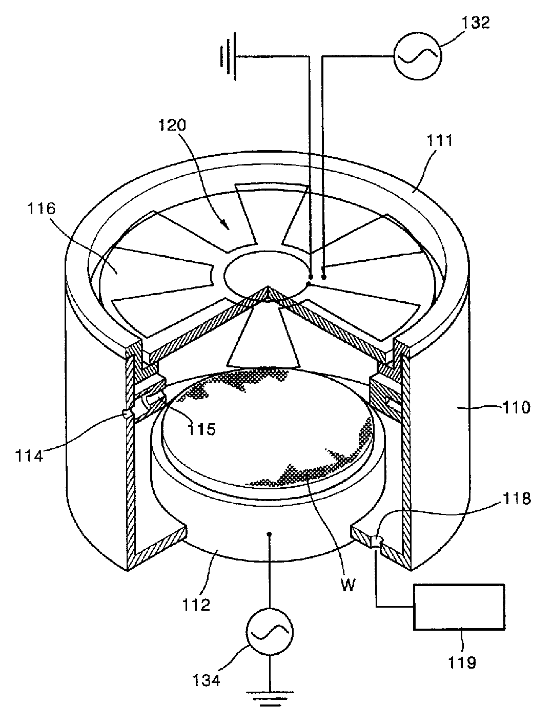
图6是根据本发明第一实施例的包含有曲折线圈的ICP发生设备的分解透视图,而图7是图6中的曲折线圈天线的放大透视图。图6的ICP发生设备是半导体制造设备,用于精加工衬底、即晶片W,例如利用由天线120产生的等离子体蚀刻或沉积晶片W上的特定材料。6 is an exploded perspective view of an ICP generating device including a meander coil according to a first embodiment of the present invention, and FIG. 7 is an enlarged perspective view of the meander coil antenna in FIG. 6 . The ICP generating apparatus of FIG. 6 is a semiconductor manufacturing apparatus for finishing a substrate, ie, a wafer W, such as etching or depositing a specific material on the wafer W using plasma generated by the
参照图6,ICP发生设备包括反应室110,反应室110包含用于产生等离子体的空间。反应室110的内侧保持真空状态,并且为此目的,在反应室110的底部处设置真口吸取口118,且该吸取口118连接到真空泵119上。用于支撑衬底、例如晶片W的静电卡盘112设置在反应室110之内的下部处,而RF电源134连接到静电卡盘112上,以提供偏置电压,从而使反应室110内产生的等离子体的离子能够以足够高的能量与晶片W的表面碰撞。介电窗口116安装在反应室110的上盖111处,以便传递RF功率。气体供给口114形成在反应室110的侧壁处,以便将反应气体供给到反应室110。可以在反应室110之内设置多个连接到气体供给口114上的气体配送口115。Referring to FIG. 6, the ICP generating apparatus includes a
天线120设置在反应室110的顶部上,即,设置在介电窗口116之上,以便感应电场,从而通过离子化供给到反应室110中的反应气体来产生等离子体。RF电源132连接到天线120上,以便向其提供RF功率。随着RF电流在形成天线120的线圈内流动,根据安培右手定律产生磁场。由于磁场作为时间的函数变化,根据电磁感应的法拉第定律在反应室120内感应出电场。感应出的电场加速电子,而被加速的电子将通过气体配送口115供给到反应室120内的反应气体离子化,从而产生等离子体。The
如图7所示,天线120包括放置在中心部分处的圆形线圈122、以及围绕圆形线圈122的曲折线圈124。曲折线圈124具有锯齿形图案,带有沿着天线120周边等间隔的各部分。锯齿形图案的数量可以根据天线120的半径而有所变化。虽然在图7中出现六个锯齿形图案,但是对于较大半径的天线,可以出现八个或更多个锯齿形图案,而对于较小半径的天线,可以出现少于六个锯齿形图案。另外,曲折线圈124包括多个外部124a,它们沿着圆周延伸,并包括多个内部124b,它们朝向放置在中心部分处的圆形线圈122弯曲。内部124b靠近圆形线圈122放置,以逐渐增大磁场分量的大小。同时,在曲折线圈124外部124a处产生的磁场分量的大小向外剧烈减小。外部124A与反应室110内的晶片W的边缘部分对齐。对于给定的线圈长度,曲折线圈124的面积小于传统圆形线圈的面积,从而具有曲折线圈124的天线120的电感与传统圆形线圈相比有所减小。As shown in FIG. 7 , the
虽然在图6和图7中曲折线圈124的角部呈现出锋利的,但是,为了便于制造,曲折线圈124的角部可以倒圆。曲折线圈124的这种可选结构可以应用在下面描述的所有实施例中。Although the corners of the meander coil 124 appear sharp in FIGS. 6 and 7 , the corners of the meander coil 124 may be rounded for ease of manufacture. This optional configuration of the meander coil 124 can be applied in all the embodiments described below.
圆形线圈122的半径以及曲折线圈124的内径和外径可以根据反应室110的尺寸充分调整。尤其是,为了减小电容耦合效应,优选的是将圆形线圈122的半径以及曲折线圈124的内径减小得尽可能小。这是由于曲折线圈124中与圆形线圈122相邻的内部124b的面积较小有助于减小天线120的电容。然而,如果圆形线圈122的半径和曲折线圈124的内径过小,则难于制造在圆形线圈122和曲折线圈124中具有冷却剂通道的结构(这将在后面予以描述),并且电阻增大。因此,圆形线圈122的半径和曲折线圈124的内径应当在考虑这种预期问题的前提下加以确定。The radius of the circular coil 122 and the inner and outer diameters of the meandering coil 124 can be adjusted substantially according to the size of the
当在线圈122和124中形成冷却剂通道(未示出)时,线圈122和124可以具有圆形横截面,以允许冷却剂通过冷却剂通道平滑流动。线圈122和124的圆形横截面有利地防止了由于在线圈122和124表面上电流不规则分布带来的电阻增大。When coolant passages (not shown) are formed in the coils 122 and 124 , the coils 122 and 124 may have a circular cross section to allow the coolant to flow smoothly through the coolant passages. The circular cross-section of the coils 122 and 124 advantageously prevents an increase in electrical resistance due to irregular distribution of current across the surfaces of the coils 122 and 124 .
在具有上述结构地曲折线圈天线120中,磁场在反应室110中的分布可以通过优化圆形线圈122的直径、曲折线圈124的内径和外径之间的差、以及锯齿形图案的数量来加以调节。磁场分布直接影响在反应室110内产生的等离子体的密度的均匀性。因此,等离子体密度分布均匀性可以通过适当调节磁场分布来加以改善。这将在下面予以描述。In the
圆形线圈122的一端部接地,而曲折线圈124的一端部连接到RF电源132。另外,圆形线圈122的一端部可以连接到RF电源132,而曲折线圈124的一端部可以接地。圆形线圈122和曲折线圈124的另一端连接到连接线圈128上。连接线圈128放置在比圆形线圈122和曲折线圈124所处平面高的地方,结果,连接线圈128对等离子体发生的影响可以忽略。One end of the circular coil 122 is grounded, while one end of the meander coil 124 is connected to an
优选的是,圆形线圈122和曲折线圈124具有宽度小于高度的恒定矩形横截面。天线120的电感可以通过这种窄线圈122和124得以减小。这将参照图8详细描述。Preferably, the circular coil 122 and the meander coil 124 have a constant rectangular cross-section with a width smaller than a height. The inductance of the
图8是对于具有不同横截面宽度的线圈,电感(L)相对于高度的曲线。各自由三个圆形线圈构成的天线用于计算电感(L),其中三个圆形线圈分别具有7cm、14cm和21cm的半径,并且每个线圈的横截面的宽度和高度变化。假设恒定的电流流过每个线圈的表面。Figure 8 is a graph of inductance (L) versus height for coils having different cross-sectional widths. Antennas each consisting of three circular coils each having a radius of 7 cm, 14 cm and 21 cm, each of which varies in width and height of the cross-section were used to calculate the inductance (L). Assume a constant current flows across the surface of each coil.
从图8可以看出,当线圈的横截面面积随着横截面的宽度或高度变大而增大时,天线的电感下降。另外,对于给定的横截面面积,较窄宽度且较大高度的线圈的电感小于较大宽度而较小高度的线圈的电感。对于具有36mm2的相同横截面面积的两个线圈,1mm宽度、36mm高度的横截面的线圈的电感L1低于6mm宽度、6mm高度横截面的其他线圈的电感L2。It can be seen from FIG. 8 that when the cross-sectional area of the coil increases as the width or height of the cross-section becomes larger, the inductance of the antenna decreases. Additionally, for a given cross-sectional area, the inductance of a coil of narrower width and greater height is less than the inductance of a coil of greater width and height. For two coils with the same cross-sectional area of 36mm2, the inductance L1 of the coil of 1 mm width, 36 mm height cross section is lower than the inductance L2 of the other coil of 6 mm width, 6 mm height cross section.
回来参照图7,圆形线圈122和曲折线圈124沿相反方向缠绕。因此,电流沿相反方向流过圆形线圈122和曲折线圈124,从而天线的电感被有利地降低。这将参照图9加以描述。然而,如果需要的话,圆形线圈122和曲折线圈124可以沿相同方向缠绕。Referring back to FIG. 7, the circular coil 122 and the meander coil 124 are wound in opposite directions. Accordingly, current flows in opposite directions through the circular coil 122 and the meander coil 124, whereby the inductance of the antenna is advantageously reduced. This will be described with reference to FIG. 9 . However, the circular coil 122 and the meander coil 124 can be wound in the same direction, if desired.
图9是示出天线电感L相对于线圈数量、线圈形状和电流流过线圈的方向变化的曲线。在图9中,曲线①表示在电流沿相同方向流过所有线圈时,由四个圆形线圈构成的天线的计算电感,其中四个线圈分别具有5.25cm、10.5cm、15.75cm、和21cm的半径;曲线②表示当电流沿相同方向流过所有线圈时由三个圆形线圈构成的天线的计算电感,其中三个圆形线圈分别具有7cm、14cm、和21cm的半径;曲线③表示当电流沿相反方向流过相邻线圈时与曲线①相同的天线的计算电感;而曲线④表示当电流沿相反方向流过相邻线圈时与曲线②相同的天线的计算电感。FIG. 9 is a graph showing changes in the antenna inductance L with respect to the number of coils, the shape of the coils, and the direction in which current flows through the coils. In Fig. 9,
如从图9中清楚看到的,对于具有较少线圈(曲线②和④)的天线,当电流沿相反方向流过天线的相邻线圈时电感较低。电流流过天线的线圈的方向对电感的影响似乎比线圈的数量对电感的影响大。换句话说,当使电流沿相反方向流过相邻线圈时,天线的电感可以明显降低,即使具有较多的线圈。As is clear from Fig. 9, for an antenna with fewer coils (
如在上述实施例中所描述的,可以通过改变构成天线的线圈的横截面形状以及流过线圈的电流的方向来有效降低天线的电感。于是,较高频率的RF功率可以施加到天线上。As described in the above embodiments, the inductance of the antenna can be effectively reduced by changing the cross-sectional shape of the coil constituting the antenna and the direction of the current flowing through the coil. Thus, higher frequency RF power can be applied to the antenna.
图10是在根据本发明第二实施例的ICP发生设备中的曲折线圈天线的平面图。图10的天线220包括放置在天线220的中心部分处的第一圆形线圈222、围绕第一圆形线圈222放置的曲折线圈224、以及围绕曲折线圈224放置的第二圆形线圈226。即,与图7的天线120相比,图10的天线220具有在最外部还包括另外的圆形线圈226的结构。曲折线圈224的形状、功能和效果与图7的曲折线圈124的相同,因此在这里不再重复对它的描述。第二圆形线圈226放置成非常靠近曲折线圈224的周边,例如,具有大约1cm的间隔间隙。图10的天线220具有的优点为由于最外面的第二圆形线圈226的存在,在天线220边缘附近产生的等离子体的密度与图7所示的天线120相比更高。此外,峰值磁场可以沿天线220的径向朝外周边移位。这将在后面描述。Fig. 10 is a plan view of a meander coil antenna in an ICP generating device according to a second embodiment of the present invention. The
第一圆形线圈222的一端部接地,而第二圆形线圈226的一端部连接到RF电源232。第一圆形线圈222和第二圆形线圈226的另一端部通过连接线圈228a和228b分别连接到曲折线圈224的端部上。连接线圈228a和228b放置在第一和第二圆形线圈222和226以及曲折线圈124所处平面之上足够高处,以便对等离子体产生的影响最小。One end of the first
第一圆形线圈222、曲折线圈224和第二圆形线圈226可以具有高度大于宽度的矩形横截面。另外,如果需要的话,第一圆形线圈222、曲折线圈224和第二圆形线圈226可以具有圆形横截面。另外,相邻的线圈沿相反的方向缠绕,以使得电流沿相反方向流过它们。有利地是,具有图10所示结构的天线220具有较低的电感,如参照图7的天线120所描述的那样。The first
图11是在根据本发明第三实施例的ICP发生设备中的曲折线圈天线的平面图。图11的天线320包括放置在天线320中心部分处的圆形线圈322、围绕圆形线圈322放置的第一曲折线圈324、以及围绕第一曲折线圈324放置的第二曲折线圈326。即,与图7的天线120相比,图11的天线320具有在最外部分处还包括另外的曲折线圈326的结构。换句话说,图11的天线320的结构可以通过将图10的天线220的最外部第二圆形线圈226由第二曲折线圈326替代来实现。第一曲折线圈324与图7的天线120的曲折线圈124相同。第二曲折线圈326的外周边弯曲成锯齿形图案,与第一曲折线圈324类似,并具有与第一曲折线圈324同样多的锯齿形,并且每个锯齿形之间的间隔相同。此外,第二曲折线圈326的内部(沟槽部分)的半径(以下称为内径)可以小于第一曲折线圈324的外部(凸脊部分)的半径(以下称为外径)。即,第二曲折线圈326的内部可以相对于第一曲折线圈324的外部凹入。Fig. 11 is a plan view of a meander coil antenna in an ICP generating device according to a third embodiment of the present invention. The
在具有这种结构的天线320中,在反应室边缘部分处的磁场分布可以通过第二曲折线圈326来轻易加以控制。即,在反应室中等离子体密度的均匀性可以通过适当将最外部第二曲折线圈326设计成锯齿形图案而得以优化。In the
如图13所示,当天线具有适当的锯齿形图案的附加最外部曲折线圈时,与带有多于一圈的图12G所示的三圈天线类似,与不带有最外部曲折线圈的图12E所示的两圈线圈天线相比,天线的电感可以降低。As shown in Figure 13, when the antenna has additional outermost meander coils in an appropriate zigzag pattern, similar to the three-turn antenna shown in Figure 12G with more than one turn, as in Figure 12G without the outermost meander coil The inductance of the antenna can be reduced compared to the two-turn coil antenna shown in 12E.
返回参照图11,圆形线圈322的一端部接地,而第二曲折线圈326的一端部连接到RF电源332。圆形线圈332和第二曲折线圈326与第一曲折线圈324的连接、以及为此连接线圈328a和328b的布置与上述实施例中的相同。另外,线圈322、324和326的横截面形状、线圈322、324和326缠绕的方向、电流流过线圈322、324和326的方向以及它们的效果也与上述实施例的相同。Referring back to FIG. 11 , one end of the
将参照图12A到12G以及图13描述曲折线圈天线的各种示例、由每种曲折线圈天线产生的径向磁场分量Br的分布以及每种曲折线圈天线的电感。Various examples of the meander coil antenna, the distribution of the radial magnetic field component Br generated by each meander coil antenna, and the inductance of each meander coil antenna will be described with reference to FIGS. 12A to 12G and FIG. 13 .
图12A到图12G的左侧上的图象示出各种曲折线圈天线的结构以及由每种天线产生的径向磁场分量Br的分布。图12A到图12G右侧上的曲线示出作为距每个天线中心的距离的函数的径向磁场分量的大小。该数据是通过在穿过每个天线中点的三条任意水平线之下5cm处模拟径向磁场分布而获得的。对于这种模拟,假设通过每个天线的每个线圈的电流的横截面分布均匀一致。The images on the left side of FIGS. 12A to 12G show the structures of various meander coil antennas and the distribution of the radial magnetic field component Br generated by each antenna. The curves on the right side of FIGS. 12A-12G show the magnitude of the radial magnetic field component as a function of distance from the center of each antenna. The data were obtained by simulating the radial magnetic field distribution at 5 cm below three arbitrary horizontal lines passing through the midpoint of each antenna. For this simulation, it is assumed that the cross-sectional distribution of current through each coil of each antenna is uniform.
图13是针对图4A和4B的圆形线圈天线和图12A到图12G的曲折线圈天线的计算电感L的曲线。13 is a graph of the calculated inductance L for the circular coil antenna of FIGS. 4A and 4B and the meander coil antenna of FIGS. 12A-12G .
图12A的天线包括放置在其中心部分处的半径7cm的圆形线圈,以及两个平均半径分别为14cm和21cm的曲折线圈,它们围绕圆形线圈放置。具有14cm平均半径的曲折线圈具有锯齿形图案,带有等间隔的四个部分,其外径比其内径大2cm。具有21cm平均半径的曲折线圈具有锯齿形图案,带有等间隔的十二个部分,其外径比其内径大6m。此外,每个线圈具有6mm×6mm的方形横截面,电流沿相反方向流过相邻的线圈。The antenna of FIG. 12A includes a circular coil of
在图12A的天线中,中心圆形线圈具有恒定的半径,而最外部线圈在其外径和内径之间具有较大的差异,并且比在最内侧圆形和最外侧线圈之间的线圈更曲折。具有这种结构的天线的电感相对低,如图13所示。参照图12A的曲线,该曲线示出磁场分布,有利地是,与图4B的天线相比,最外侧的峰值较宽,并且稍微向外偏移。然而,由于最外侧峰值的高度减小,而内侧峰值的高度无变化,因此难于预期等离子体的均匀性得到改善。In the antenna of FIG. 12A , the central circular coil has a constant radius, while the outermost coil has a larger difference between its outer and inner diameters and is wider than the coils between the innermost circular and outermost coils. tortuous. The inductance of the antenna with this structure is relatively low, as shown in Figure 13. Referring to the graph of Fig. 12A, which shows the magnetic field distribution, advantageously the outermost peaks are wider and slightly shifted outwards compared to the antenna of Fig. 4B. However, since the height of the outermost peak decreases while the height of the inner peak does not change, it is difficult to expect the uniformity of the plasma to be improved.
图12B的天线包括分别具有7cm和16.1cm半径的两个圆形线圈,它们放置在自天线中心起的第一和第三位置处,并包括分别具有10.3和21cm平均半径的两个曲折线圈,它们放置在自天线中心起第二和第四位置处。具有10.3cm平均半径的曲折线圈具有锯齿图案,带有等间隔的八个部分,其外径比其内径大5.4cm。具有21cm平均半径的曲折线圈具有锯齿形图案,带有等间隔的八个部分,其外径比其内径大8cm。此外,每个线圈具有6mm×6mm的横截面,而电流沿相反方向流过相邻线圈。The antenna of FIG. 12B includes two circular coils with radii of 7 cm and 16.1 cm, respectively, placed at first and third positions from the center of the antenna, and includes two meandering coils with average radii of 10.3 and 21 cm, respectively, They are placed at the second and fourth positions from the center of the antenna. A meander coil with an average radius of 10.3 cm had a zigzag pattern with eight equally spaced sections, and its outer diameter was 5.4 cm larger than its inner diameter. A meander coil with an average radius of 21 cm has a zigzag pattern with eight equally spaced sections, the outer diameter of which is 8 cm larger than its inner diameter. In addition, each coil has a cross-section of 6 mm x 6 mm, and current flows through adjacent coils in opposite directions.
在图12B的天线中,尽管线圈的数量增大,但是天线的电感仍然较低,如图13所示。此外,有利地是,在图12B的磁场分布曲线中,最外侧峰值具有较大的宽度,而内侧峰值的大高度显著减小。于是,可以预期利用具有图12B结构的天线可以改善等离子体的均匀性。In the antenna of FIG. 12B , although the number of coils is increased, the inductance of the antenna is still low, as shown in FIG. 13 . Furthermore, advantageously, in the magnetic field profile of FIG. 12B , the outermost peaks have a greater width, while the greater height of the inner peaks is significantly reduced. Thus, it can be expected that the uniformity of plasma can be improved by using the antenna having the structure of FIG. 12B.
图12C的天线包括半径16.1cm的圆形线圈和平均半径21cm的曲折线圈,该曲折线圈围绕圆形线圈放置。曲折线圈具有锯齿形图案,带有等间隔的八个部分,且外径比其内径大8cm。此外,每个线圈具有6mm×6mm的方形横截面,而电流沿相反方向流过两个线圈。The antenna of FIG. 12C includes a circular coil with a radius of 16.1 cm and a meander coil with an average radius of 21 cm placed around the circular coil. The meander coil has a zigzag pattern with eight equally spaced sections and an
图12C的天线具有比图12B的天线简单的结构,但具有相同的结构优点。图12C的天线的电感相当低,如图13所示,并且磁场分布具有两个远离线圈中心定位的分离的峰值。于是,在图12C所示的天线中,可以预期等离子体均匀性可得以显著改善。The antenna of Fig. 12C has a simpler structure than the antenna of Fig. 12B, but has the same structural advantages. The inductance of the antenna of Figure 12C is rather low, as shown in Figure 13, and the magnetic field distribution has two separate peaks located away from the center of the coil. Thus, in the antenna shown in FIG. 12C, it can be expected that plasma uniformity can be significantly improved.
图12D的天线包括半径3cm的圆形线圈,以及平均半径为14.3cm的曲折线圈,其中圆形线圈放置在天线的中心部分处,而曲折线圈围绕圆形线圈放置。曲折线圈具有锯齿形图案,带有等间隔的八个部分,外径比其内径大22cm。此外,每个线圈具有6mm×6mm的方形横截面,而电流沿相反方向流过两个线圈。The antenna of FIG. 12D includes a circular coil with a radius of 3 cm, and a meander coil with an average radius of 14.3 cm, wherein the circular coil is placed at the central portion of the antenna and the meander coil is placed around the circular coil. The meander coil has a zigzag pattern with eight equally spaced sections, with an outer diameter 22 cm larger than its inner diameter. In addition, each coil has a square cross-section of 6 mm x 6 mm, and current flows through the two coils in opposite directions.
图12D的天线具有与图12C的天线类似的结构,但是其中心的圆形线圈的半径小于图12C的天线的圆形线圈的半径。对于具有图12D结构的天线,其电感仍然低于图4A所示的简单传统圆形线圈天线,尽管它与图12C的天线相比稍大。对于图12D的天线,由于圆形线圈和曲折线圈相对部分的面积小于图12C的天线的,可以预期电容以及电容耦合效应减小。如从图12D中的磁场分布中明显看出的,通过优化中心圆形线圈的半径、曲折线圈内径和外径之间的差、以及在曲折线圈中锯齿形图案的数量,可以将等离子体均匀性改善到大于简单的圆形线圈天线和螺旋线圈天线。The antenna of Fig. 12D has a similar structure to the antenna of Fig. 12C, but the radius of the circular coil at the center is smaller than that of the antenna of Fig. 12C. For the antenna with the structure of Fig. 12D, its inductance is still lower than that of the simple conventional circular coil antenna shown in Fig. 4A, although it is slightly larger compared to the antenna of Fig. 12C. For the antenna of FIG. 12D , since the area of the opposing portions of the circular coil and the meander coil is smaller than that of the antenna of FIG. 12C , capacitance and capacitive coupling effects can be expected to be reduced. As evident from the magnetic field distribution in Fig. 12D, by optimizing the radius of the central circular coil, the difference between the inner and outer diameters of the meandering coils, and the number of zigzag patterns in the meandering coils, the plasma can be uniformly performance is improved over simple circular coil antennas and helical coil antennas.
图12E的天线是具有上面参照图6和7描述的结构的曲折天线。图12E的天线具有与图12D的天线相同的线圈几何形状。而且,与图12D的天线类似,电流沿相反方向流过图12E所示天线的两个线圈。然而,为了考察矩形线圈横截面的效果,图12E的天线设计成具有1mm宽、36mm高的矩形线圈横截面,这与图12D的天线不同。The antenna of FIG. 12E is a meander antenna having the structure described above with reference to FIGS. 6 and 7 . The antenna of Figure 12E has the same coil geometry as the antenna of Figure 12D. Also, similar to the antenna of FIG. 12D, current flows in opposite directions through the two coils of the antenna shown in FIG. 12E. However, in order to examine the effect of the rectangular coil cross-section, the antenna of FIG. 12E is designed to have a rectangular coil cross-section of 1 mm wide and 36 mm high, which is different from the antenna of FIG. 12D .
对于具有图12E的结构的天线,电感比图12D的天线的电感显著低,如图13所示。图12E的天线的磁场分布类似于图12D的天线的磁场分布,除了与图12D的天线相比,磁场强度朝向外边缘增大得更平稳之外。于是,除了图12D的天线的优点以为,由于图12E的天线具有较低的电感,可以实现在高频处的感应耦合等离子体放电。For the antenna having the structure of FIG. 12E , the inductance is significantly lower than that of the antenna of FIG. 12D , as shown in FIG. 13 . The magnetic field distribution of the antenna of FIG. 12E is similar to that of the antenna of FIG. 12D , except that the magnetic field strength increases more smoothly towards the outer edge compared to the antenna of FIG. 12D . Thus, in addition to the advantages of the antenna of Fig. 12D, it is possible to achieve inductively coupled plasma discharges at high frequencies due to the lower inductance of the antenna of Fig. 12E.
图12F的天线是与图10所示天线相同的类型。图12F的天线在图12E的天线的基本线圈几何形状上还包括最外侧的圆形线圈。最外侧圆形线圈与内部曲折线圈间隔1cm。每个线圈如上所述具有矩形横截面,并且电流沿相反方向流过相邻线圈。The antenna of FIG. 12F is of the same type as the antenna shown in FIG. 10 . The antenna of Figure 12F also includes an outermost circular coil over the basic coil geometry of the antenna of Figure 12E. The outermost circular coil was separated from the inner meander coil by 1 cm. Each coil has a rectangular cross-section as described above, and current flows through adjacent coils in opposite directions.
对于具有图12F的结构的天线,如图13所示,电感仍然较低。另外,由于最外侧的圆形线圈,由内部圆形线圈和曲折线圈产生的峰值磁场与图12E的天线相比向外稍微偏移。于是,靠近天线边缘部分的等离子体密度增大。For the antenna with the structure of Fig. 12F, as shown in Fig. 13, the inductance is still lower. In addition, due to the outermost circular coils, the peak magnetic fields generated by the inner circular coils and meander coils are slightly shifted outward compared to the antenna of Figure 12E. Then, the plasma density near the edge portion of the antenna increases.
根据本发明的第三实施例,图12G的天线为与图11的天线相同的类型。图12G的天线在图12E的天线的基本线圈几何形状上还包括最外侧曲折线圈。换句话说,图12F天线的最外侧圆形线圈用曲折线圈替代。每个线圈具有矩形横截面,如上所述,并且电流沿相反方向流过相邻线圈。According to a third embodiment of the invention, the antenna of FIG. 12G is of the same type as the antenna of FIG. 11 . The antenna of Figure 12G also includes an outermost meander coil over the basic coil geometry of the antenna of Figure 12E. In other words, the outermost circular coil of the antenna of FIG. 12F is replaced with a meander coil. Each coil has a rectangular cross-section, as described above, and current flows through adjacent coils in opposite directions.
对于具有图12G结构的天线,如图13所示,电感仍然较低。在径向和周向上的最外侧磁场分布可以通过调节最外侧曲折线圈来加以调节。于是,可以预期通过将最外侧曲折线圈构造成适当图案可以优化等离子体的均匀性。For the antenna with the structure of Fig. 12G, as shown in Fig. 13, the inductance is still lower. The outermost magnetic field distribution in the radial and circumferential directions can be adjusted by adjusting the outermost meander coil. Thus, it is expected that the uniformity of the plasma can be optimized by configuring the outermost meander coils in an appropriate pattern.
关于感应耦合等离子体放电,当高电压施加到天线上时,由于电容耦合产生高的等离子体电势,并且等离子体发生效率和等离子体均匀性恶化。因此,在设计天线时,应该考虑使电容耦合效应最小。在增大频率以产生高密度且电子温度低的等离子体并改善在低压下等离子体放电的感应耦合效率的情况下,需要低感抗天线,以用于有效的阻抗匹配。如上所述,根据本发明的天线具有曲折线圈,该曲折线圈较长,但却占据较少面积。在根据本发明的天线中,电流沿相反方向流过相邻线圈,并且每个线圈具有高度大于宽度的横截面。于是,天线的电感相当低。当利用这种低电感天线时,即使施加高的RF频率时,阻抗也可非常低,并可以降低天线两端的电势差,由此减小了电容耦合效应。另外,可以防止被离子与介电窗口碰撞时所产生的颗粒污染。此外,中心圆形线圈的半径越小,中心圆形线圈和外部线圈的相对部分的面积就越小,并且天线的电容也就越小。当线圈具有较小的宽度时,线圈中面对介电窗口的部分的面积减小,从而使与等离子体的电容耦合效应最小。Regarding inductively coupled plasma discharge, when a high voltage is applied to the antenna, a high plasma potential is generated due to capacitive coupling, and plasma generation efficiency and plasma uniformity deteriorate. Therefore, when designing the antenna, consideration should be given to minimizing the effect of capacitive coupling. With increasing frequency to generate high density plasma with low electron temperature and improve inductive coupling efficiency of plasma discharges at low pressure, low inductance antennas are required for effective impedance matching. As described above, the antenna according to the present invention has a meander coil which is long but occupies less area. In the antenna according to the invention, currents flow through adjacent coils in opposite directions, and each coil has a cross-section whose height is greater than its width. Thus, the inductance of the antenna is relatively low. When such a low inductance antenna is utilized, the impedance can be very low even when high RF frequencies are applied, and the potential difference across the antenna can be reduced, thereby reducing capacitive coupling effects. In addition, contamination by particles generated when ions collide with the dielectric window can be prevented. In addition, the smaller the radius of the central circular coil, the smaller the area of the opposing portion of the central circular coil and the outer coil, and the smaller the capacitance of the antenna. When the coil has a smaller width, the area of the portion of the coil facing the dielectric window is reduced, thereby minimizing the capacitive coupling effect with the plasma.
图14是示出根据本发明第四实施例中ICP发生设备中的曲折线圈天线和永久磁铁的布置的平面图。参照图14,曲折线圈天线420安装在反应室410的上部,而多个永久磁铁440布置在反应室410的外测。多个永久磁铁440沿着反应室410的周边布置,使得他们的N磁极和S磁极交替。14 is a plan view showing the arrangement of a meander coil antenna and a permanent magnet in an ICP generating device according to a fourth embodiment of the present invention. Referring to FIG. 14 , a
曲折线圈天线420包括圆形线圈422,该线圈定位在天线的中心部分处,并包括第一和第二曲折线圈424和426,它们围绕圆形线圈422布置。曲折线圈天线420具有与根据第三实施例的图11中的曲折线圈天线相同的结构,并因此不再重复对它的详细描述。曲折线圈天线420可以由上述根据第一或第二实施例的曲折线圈天线替代。The
优选的是,多个永久磁铁440位于由天线420产生的磁场的大小相对弱的区域处。对于天线420,在如图12G所示第一和第二曲折线圈424和426的外部彼此靠近的区域中、在磁场大小相对弱的地方,永久磁铁440布置成与第一和第二曲折线圈424和426的外部相对应。It is preferable that the plurality of
当天线440的结构改变使得磁场分布变化时,优选的是,永久磁铁440的位置变化。为此目的,优选的是,永久磁体440布置成它们可围绕反应室410同时回转,以变换它们的位置。When the structure of the
在本实施例中,为了抵消在曲折线圈天线420中产生的局部磁极效应,多个永久磁铁440布置在反应室410的外测。如此布置的永久磁铁440产生一种所谓的多磁极限制效应,这是指等离子体受到永久磁铁440的磁场的限制。换句话说,在永久磁铁440沿着反应室440的周边布置以使它们的N和S磁极交替时,在靠近反应室410的内壁处诱发磁镜效应,充电颗粒的壁损耗减小,靠近反应室410的内壁处的等离子体密度增加,从而改善了等离子体密度的均匀性。由永久磁体440产生的磁场在反应室410的侧壁附近汇聚,从而,在反应室410内产生的大部分等离子体不会受到永久磁体440产生的磁场的影响。对于在外部其磁场相对弱的曲折线圈天线420,当永久磁铁440位于具有相对弱磁场的外部时,多磁极限制效应更有效。In this embodiment, in order to counteract the local magnetic pole effect generated in the
如上所述,根据图14所示的实施例,由于借助于多磁极限制效应使得电子的壁损耗下降,因此在反应室内的等离子体密度和等离子体均匀性得以增大。另外,当围绕天线布置的永久磁铁的位置可以方便地变化时,可以针对不同的工艺条件优化等离子体的特性。As described above, according to the embodiment shown in FIG. 14, since the wall loss of electrons is reduced by virtue of the multi-pole confinement effect, the plasma density and plasma uniformity in the reaction chamber are increased. In addition, when the position of the permanent magnets arranged around the antenna can be easily varied, the properties of the plasma can be optimized for different process conditions.
图15是示出在根据本发明第五实施例的ICP发生设备中曲折线圈天线、匹配网络、以及电容器的布置的平面图。参照图15,匹配网络530连接到RF电源532和曲折线圈天线520之间,而电容器534连接到曲折线圈天线520和匹配网络530之间,与曲折线圈天线520平行。15 is a plan view showing the arrangement of a meander coil antenna, a matching network, and capacitors in an ICP generating device according to a fifth embodiment of the present invention. Referring to FIG. 15 , the
曲折线圈天线520包括位于其中心部分处的圆形线圈522、以及围绕圆形线圈522布置的第一和第二曲折线圈524和526。曲折线圈天线520具有与根据本发明第三实施例的图11中的曲折线圈天线相同的结构,并因此不在此重复对它的详细描述。曲折线圈天线520可以由上述根据第一或第二实施例的曲折线圈天线替代,或者,曲折线圈天线520也可以由传统圆形线圈天线或螺旋线圈天线替代。换句话说,根据本发明第五实施例的ICP发生设备与任意类型天线兼容。The
构成曲折线圈天线520的圆形线圈522和第一及第二曲折线圈524和526可以串联到RF电源532上。尽管未示出,线圈522、524和526中的一些或所有的可以并联到RF电源532上。换句话说,电容器534总是并联到RF电源532上,而构成曲折线圈天线520的线圈522、524和526可以串联或并联到RF电源532上。如果需要的话,可以通过将线圈522、524和526串联或并联到RF电源532上来适当地调节天线520的电感。The
在图15所示的实施例中,由于电容器534并联在曲折线圈天线520和匹配网络530之间,可以利用LC谐振现象来更易地进行起始(initial)等离子体放电,并确保利用感应耦合等离子体稳定地加工。In the embodiment shown in FIG. 15, since the
如上所述,关于ICP放电,在施加较高的天线电压时,起始等离子体放电通过电容耦合来诱发,并然后通过流过天线线圈的AC电流所感应的电场实现感应耦合放电。起始电容耦合所需的阈值击穿电压取决于加工压力或加工气体。对于具有沿相反方向缠绕的相邻线圈并具有较低电感的天线,应该施加非常高的RF功率,以导致天线中的电势差较大。否则,不能诱发需要较大电势差的借助电容耦合的起始等离子体放电。然而,在利用可以通过适当地预先设定匹配网络来诱发的LC谐振现象时,借助电容耦合实现的起始等离子体放电的较大电势差可以利用这种低电感天线诱发出来。这将参照图16和图17A到图17D予以描述。As described above, regarding the ICP discharge, when a high antenna voltage is applied, an initial plasma discharge is induced by capacitive coupling, and then an inductively coupled discharge is realized by an electric field induced by an AC current flowing through the antenna coil. The threshold breakdown voltage required to initiate capacitive coupling depends on process pressure or process gas. For antennas with adjacent coils wound in opposite directions and with lower inductance, very high RF power should be applied to cause a larger potential difference in the antenna. Otherwise, an initial plasma discharge by means of capacitive coupling, which requires a large potential difference, cannot be induced. However, larger potential differences for initiating plasma discharges by means of capacitive coupling can be induced with such low-inductance antennas while exploiting the LC resonance phenomenon that can be induced by suitably presetting the matching network. This will be described with reference to FIG. 16 and FIGS. 17A to 17D.
图16是连接到ICP天线上的L型匹配网络的电路图,而图17A到17D是用于解释当图15的电容器的电抗变化时的LC谐振现象的曲线。16 is a circuit diagram of an L-shaped matching network connected to an ICP antenna, and FIGS. 17A to 17D are graphs for explaining the LC resonance phenomenon when the reactance of the capacitor of FIG. 15 varies.
参照图16,连接RF电源532和天线520的匹配网络530包括两个可变电容器C1和C2。此外,对应于图15中的电容器534的电容器C3并联在匹配网络530和天线520之间。考虑到匹配网络530中的电阻损耗,将电阻器R1包括在图16的等效电路中。Referring to FIG. 16, the
图17A是阻抗对电抗的曲线,用于解释谐振现象,图17B是对于图17A中的预设点的放大曲线。在图17A和图17B中,ReZ表示天线阻抗Z的实部。Fig. 17A is a curve of impedance versus reactance for explaining the resonance phenomenon, and Fig. 17B is an enlarged curve for a preset point in Fig. 17A. In FIGS. 17A and 17B , ReZ represents the real part of the antenna impedance Z. In FIG.
如图17A和17B所示,天线的输入阻抗Z由并联于天线的电容器C3改变,例如,当RF频率为13.56MHz,且天线520的阻抗La为300nH、电阻R0为0.1欧姆时,在电容器(C3)的电抗Xc为25.65欧姆(即,C=458pF)时发生LC谐振。由于ICP天线的Q因数在产生等离子体之前要比产生等离子体之后大,出现一个窄的谐振峰值。天线的阻抗Z在针对给定RF功率的谐振点处极大地增加,从而天线具有过大的电压差,而不能匹配RF功率。除非满足匹配条件,否则发生明显的RF功率反射,不能实现有效的等离子体放电。As shown in Figures 17A and 17B, the input impedance Z of the antenna is changed by the capacitor C3 connected in parallel to the antenna. For example, when the RF frequency is 13.56MHz, and the impedance La of the
为了解决这些问题,匹配网络的预设点设定为稍微偏离谐振点。例如,如图17A和17B所示,预设点设定在电容器C3具有355pF的电容和33欧姆的电抗Xc处。在这些条件下,电抗Xc对于匹配来说足够大,并且连接到匹配网络的天线具有类似电感器的电特性。从而,利用仅由两个可变电容器C1和C2构成的L型匹配网络,就可以满足匹配条件。当图16中的电阻器R1和R2具有0.05欧姆的电阻,并且使用3米长50欧姆的电缆时,用于匹配的电容器C1和C2的电容分别为1000pF和115pF。这些电容落入在大多数匹配网络中可以轻易实现的范围内。In order to solve these problems, the preset point of the matching network is set slightly away from the resonance point. For example, as shown in FIGS. 17A and 17B , the preset point is set where the capacitor C3 has a capacitance of 355 pF and a reactance Xc of 33 ohms. Under these conditions, the reactance Xc is large enough for matching, and the antenna connected to the matching network has inductor-like electrical characteristics. Thus, with an L-shaped matching network consisting of only two variable capacitors C1 and C2 , the matching condition can be satisfied. When the resistors R1 and R2 in Figure 16 have a resistance of 0.05 ohms, and a 3-meter-long 50-ohm cable is used, the capacitances of capacitors C1 and C2 for matching are 1000pF and 115pF, respectively. These capacitances fall within a range that can be easily implemented in most matching networks.
在设定匹配网络的预设点时,在等离子体放电之前,为了满足上述计算结果,并且输入RF功率为500瓦,相对于电容器C3的电抗Xc的变化,流过ICP天线的电流和电压呈现出如图17C和17D所示的谐振特性。即,当电容器C3具有可以诱发谐振的355pF的电容时,天线电压增大到大约1600V,该电压对于导致起始等离子体放电来说足够高。在产生等离子体之后,天线谐振增大,并且天线的电压和电流减小。例如,当图16中的天线的电阻器R0的电阻从产生等离子体之前的0.1欧姆增大到产生等离子体之后的1.0欧姆时,天线的电特性如图17C和17D的曲线2所表示的那样变化。图17C和17D中的曲线1表示产生等离子体之前的谐振现象。在产生等离子体之后,匹配网络自动设定,以满足匹配条件。由于电特性的变化,即,从曲线1变化到曲线2,大量的电流流过天线,从而随着电容耦合放电,感应耦合放电加速,并且可以稳定地保持等离子体特性。When setting the preset point of the matching network, before the plasma discharge, in order to meet the above calculation results, and the input RF power is 500 watts, the current and voltage flowing through the ICP antenna with respect to the change of the reactance Xc of the capacitor C3 Resonance characteristics were exhibited as shown in Figs. 17C and 17D. That is, when the capacitor C3 has a capacitance of 355pF that can induce resonance, the antenna voltage increases to about 1600V, which is high enough to cause an initial plasma discharge. After the plasma is generated, the resonance of the antenna increases, and the voltage and current of the antenna decrease. For example, when the resistance of the resistor R0 of the antenna in FIG. 16 increases from 0.1 ohm before plasma generation to 1.0 ohm after plasma generation, the electrical characteristics of the antenna are as shown in
满足上述谐振条件的两个电容器C1和C2的电容可以根据实验的谐振条件来变化。然而,为了找到谐振条件,不需要在开始时精确设定匹配网络的预设点。为了在等离子体放电之前找到精确的谐振条件,在反应室内的压力减小到不导致等离子体放电的毫Torr量级之后接近匹配网络的预设点,并且RF功率以自动模式施加到匹配网络上。The capacitances of the two capacitors C1 and C2 satisfying the above-mentioned resonance conditions can be varied according to the experimental resonance conditions. However, in order to find the resonance condition, it is not necessary to set the preset point of the matching network precisely at the beginning. In order to find the precise resonance condition before plasma discharge, the preset point of the matching network is approached after the pressure in the reaction chamber is reduced to the milliTorr level that does not cause plasma discharge, and the RF power is applied to the matching network in automatic mode .
如上所述,利用天线和电容器之间的LC谐振现象使得起始等离子体放电更易,并且稳定地将等离子体密度保持为较高。在法拉第屏蔽安装在天线和介电窗口之间时也采用这种方法。另外,如上所述,如果需要的话,天线的电感可以通过将构成根据本发明的曲折线圈天线的线圈并联或串联来为优化等离子体放电而调节。As described above, using the LC resonance phenomenon between the antenna and the capacitor makes it easier to initiate plasma discharge and stably maintains the plasma density high. This method is also used when the Faraday shield is installed between the antenna and the dielectric window. In addition, as described above, the inductance of the antenna can be adjusted for optimizing the plasma discharge, if necessary, by connecting the coils constituting the meander coil antenna according to the present invention in parallel or in series.
如上所述,根据本发明的ICP发生设备提供了如下的效果:As described above, the ICP generating device according to the present invention provides the following effects:
首先,可以通过优化曲折线圈天线中外径和内径之间的差以及锯齿形图案的数量来控制反应室内的磁场分布,而改善等离子体密度分布的均匀性。另外,如果需要的话,通过调节线圈的横截面形状以及电流流过线圈的方向,可以有效地降低天线的电感。于是,有效的等离子体放电可以利用高频实现,并且可以使电容耦合效应最小。First, the uniformity of the plasma density distribution can be improved by controlling the magnetic field distribution in the reaction chamber by optimizing the difference between the outer and inner diameters and the number of zigzag patterns in the meander coil antenna. In addition, if necessary, the inductance of the antenna can be effectively reduced by adjusting the cross-sectional shape of the coil and the direction in which the current flows through the coil. Thus, efficient plasma discharge can be achieved with high frequencies and capacitive coupling effects can be minimized.
第二,通过将多个永久磁铁布置在反应室外侧,以用于多磁极限制效应,可以进一步改善等离子体密度的均匀性和等离子体密度。根据所使用的曲折线圈天线,等离子体的特性可以通过改变永久磁铁的位置来优化。Second, by arranging a plurality of permanent magnets outside the reaction chamber for the multi-pole confinement effect, the uniformity of the plasma density and the plasma density can be further improved. Depending on the meander coil antenna used, the properties of the plasma can be optimized by varying the position of the permanent magnets.
第三,可以通过将电容器并联在天线和L型匹配网络之间来诱发LC谐振现象,从而起始等离子体放电变得更易,并且使利用感应耦合等离子体的加工更稳定。Third, the LC resonance phenomenon can be induced by connecting a capacitor in parallel between the antenna and the L-shaped matching network, thereby making it easier to initiate plasma discharge and making the process with inductively coupled plasma more stable.
虽然本发明已经具体示出并参照其优选实施例加以描述,本领域技术人员应该理解到在不背离由所附权利要求书限定的本发明的精髓和范围前提下,可以对本发明进行各种形式和细节上的变动。While the invention has been particularly shown and described with reference to preferred embodiments thereof, it will be understood by those skilled in the art that the invention may be embodied in various forms without departing from the spirit and scope of the invention as defined in the appended claims. and changes in details.
Claims (21)
Applications Claiming Priority (3)
| Application Number | Priority Date | Filing Date | Title |
|---|---|---|---|
| KR10-2002-0062701A KR100486724B1 (en) | 2002-10-15 | 2002-10-15 | Inductively coupled plasma generating apparatus with serpentine coil antenna |
| KR62701/02 | 2002-10-15 | ||
| KR62701/2002 | 2002-10-15 |
Publications (2)
| Publication Number | Publication Date |
|---|---|
| CN1498057A CN1498057A (en) | 2004-05-19 |
| CN1248549C true CN1248549C (en) | 2006-03-29 |
Family
ID=34256431
Family Applications (1)
| Application Number | Title | Priority Date | Filing Date |
|---|---|---|---|
| CNB2003101012277A Expired - Fee Related CN1248549C (en) | 2002-10-15 | 2003-10-15 | Induction coupling plasma generating equipment containing zigzag coil antenna |
Country Status (4)
| Country | Link |
|---|---|
| US (1) | US7381292B2 (en) |
| JP (1) | JP3903034B2 (en) |
| KR (1) | KR100486724B1 (en) |
| CN (1) | CN1248549C (en) |
Families Citing this family (34)
| Publication number | Priority date | Publication date | Assignee | Title |
|---|---|---|---|---|
| US7081711B2 (en) * | 2003-10-28 | 2006-07-25 | Applied Pulsed Power, Inc. | Inductively generated streaming plasma ion source |
| US7273533B2 (en) * | 2003-11-19 | 2007-09-25 | Tokyo Electron Limited | Plasma processing system with locally-efficient inductive plasma coupling |
| KR100716720B1 (en) * | 2004-10-13 | 2007-05-09 | 에이피티씨 주식회사 | Non-Circular Plasma Source Coil |
| KR100897176B1 (en) * | 2005-07-20 | 2009-05-14 | 삼성모바일디스플레이주식회사 | Inductively Coupled Plasma Treatment Equipment |
| JP5277473B2 (en) * | 2006-11-28 | 2013-08-28 | サムコ株式会社 | Plasma processing equipment |
| KR100907438B1 (en) | 2007-01-15 | 2009-07-14 | (주)제이하라 | Plasma generator |
| JP5098882B2 (en) * | 2007-08-31 | 2012-12-12 | 東京エレクトロン株式会社 | Plasma processing equipment |
| KR101003382B1 (en) * | 2008-02-13 | 2010-12-22 | 주식회사 유진테크 | Plasma treatment apparatus and method |
| JP5399151B2 (en) * | 2008-10-27 | 2014-01-29 | 東京エレクトロン株式会社 | Inductively coupled plasma processing apparatus, plasma processing method, and storage medium |
| KR101063763B1 (en) * | 2009-01-22 | 2011-09-08 | 서울대학교산학협력단 | Plasma generation system |
| WO2011034190A1 (en) * | 2009-09-17 | 2011-03-24 | イマジニアリング株式会社 | Plasma-generation device |
| KR20120004040A (en) * | 2010-07-06 | 2012-01-12 | 삼성전자주식회사 | Plasma generator |
| JP5723130B2 (en) * | 2010-09-28 | 2015-05-27 | 東京エレクトロン株式会社 | Plasma processing equipment |
| TWI414762B (en) * | 2010-12-24 | 2013-11-11 | Univ Nat Chiao Tung | Strain sensor device |
| US8723423B2 (en) * | 2011-01-25 | 2014-05-13 | Advanced Energy Industries, Inc. | Electrostatic remote plasma source |
| US8872428B2 (en) | 2011-02-25 | 2014-10-28 | Applied Materials, Inc. | Plasma source with vertical gradient |
| US9220162B2 (en) * | 2011-03-09 | 2015-12-22 | Samsung Electronics Co., Ltd. | Plasma generating apparatus and plasma generating method |
| US9048518B2 (en) | 2011-06-21 | 2015-06-02 | Applied Materials, Inc. | Transmission line RF applicator for plasma chamber |
| JP2013134835A (en) * | 2011-12-26 | 2013-07-08 | Nissin Electric Co Ltd | Plasma processing apparatus |
| US9279179B2 (en) * | 2012-02-06 | 2016-03-08 | Taiwan Semiconductor Manufacturing Co., Ltd. | Multi coil target design |
| US9472378B2 (en) * | 2013-10-04 | 2016-10-18 | Applied Materials, Inc. | Multiple zone coil antenna with plural radial lobes |
| US9207197B2 (en) | 2014-02-27 | 2015-12-08 | Kimberly-Clark Worldwide, Inc. | Coil for magnetic induction to tomography imaging |
| US9320451B2 (en) | 2014-02-27 | 2016-04-26 | Kimberly-Clark Worldwide, Inc. | Methods for assessing health conditions using single coil magnetic induction tomography imaging |
| US9442088B2 (en) | 2014-02-27 | 2016-09-13 | Kimberly-Clark Worldwide, Inc. | Single coil magnetic induction tomographic imaging |
| KR101773448B1 (en) * | 2016-04-29 | 2017-09-01 | 세메스 주식회사 | Antenna and apparatus for treating substrate utilizing the same |
| KR101826883B1 (en) * | 2016-11-03 | 2018-02-08 | 인투코어테크놀로지 주식회사 | Inductive Coil Structure And Inductively Coupled Plasma Apparatus |
| KR101995762B1 (en) * | 2017-11-07 | 2019-07-03 | 세메스 주식회사 | Substrate treating apparatus and substrate treating method |
| US11515122B2 (en) * | 2019-03-19 | 2022-11-29 | Tokyo Electron Limited | System and methods for VHF plasma processing |
| JP7676424B2 (en) * | 2020-02-19 | 2025-05-14 | エンツーコア テクノロジー,インコーポレーテッド | Antenna structure and plasma generation device using same |
| CN111769062B (en) * | 2020-07-27 | 2025-09-19 | 上海邦芯半导体科技有限公司 | Inductive coupling reactor and working method thereof |
| EP3965139B1 (en) | 2020-09-03 | 2024-03-27 | Jozef Stefan Institute | Apparatus, system and method for sustaining inductively coupled plasma |
| CN116169001A (en) * | 2023-01-18 | 2023-05-26 | 深圳市原速光电科技有限公司 | Inductively coupled plasma device and coating equipment |
| CN116981146B (en) * | 2023-06-06 | 2026-04-14 | 兰州空间技术物理研究所 | Control system for beam divergence of helicon wave ion source |
| CN120529473B (en) * | 2025-07-23 | 2025-09-30 | 上海谙邦半导体设备有限公司 | Plasma treatment equipment |
Family Cites Families (27)
| Publication number | Priority date | Publication date | Assignee | Title |
|---|---|---|---|---|
| US5346578A (en) | 1992-11-04 | 1994-09-13 | Novellus Systems, Inc. | Induction plasma source |
| KR100238627B1 (en) * | 1993-01-12 | 2000-01-15 | 히가시 데쓰로 | Plasma processing apparatus |
| US5401350A (en) | 1993-03-08 | 1995-03-28 | Lsi Logic Corporation | Coil configurations for improved uniformity in inductively coupled plasma systems |
| JPH0850998A (en) * | 1994-08-04 | 1996-02-20 | Kokusai Electric Co Ltd | Plasma processing device |
| EP0710055B1 (en) | 1994-10-31 | 1999-06-23 | Applied Materials, Inc. | Plasma reactors for processing semi-conductor wafers |
| JP3426382B2 (en) * | 1995-01-24 | 2003-07-14 | アネルバ株式会社 | Plasma processing equipment |
| JP3595608B2 (en) | 1995-05-30 | 2004-12-02 | アネルバ株式会社 | Vacuum processing apparatus, method for removing deposited film on inner surface of vacuum vessel in vacuum processing apparatus, and method for uniforming film deposition on inner surface of vacuum vessel in vacuum processing apparatus |
| US5731565A (en) * | 1995-07-27 | 1998-03-24 | Lam Research Corporation | Segmented coil for generating plasma in plasma processing equipment |
| JP3501910B2 (en) | 1996-04-23 | 2004-03-02 | 東京エレクトロン株式会社 | Plasma processing equipment |
| WO1998042012A1 (en) * | 1997-03-17 | 1998-09-24 | Matsushita Electric Industrial Co., Ltd. | Method and device for plasma treatment |
| US6028395A (en) | 1997-09-16 | 2000-02-22 | Lam Research Corporation | Vacuum plasma processor having coil with added conducting segments to its peripheral part |
| US6164241A (en) * | 1998-06-30 | 2000-12-26 | Lam Research Corporation | Multiple coil antenna for inductively-coupled plasma generation systems |
| GB2344930B (en) * | 1998-12-17 | 2003-10-01 | Trikon Holdings Ltd | Inductive coil assembly |
| JP2000235900A (en) * | 1999-02-15 | 2000-08-29 | Tokyo Electron Ltd | Plasma processing equipment |
| US6237526B1 (en) * | 1999-03-26 | 2001-05-29 | Tokyo Electron Limited | Process apparatus and method for improving plasma distribution and performance in an inductively coupled plasma |
| JP2000331993A (en) * | 1999-05-19 | 2000-11-30 | Mitsubishi Electric Corp | Plasma processing equipment |
| US6319355B1 (en) * | 1999-06-30 | 2001-11-20 | Lam Research Corporation | Plasma processor with coil responsive to variable amplitude rf envelope |
| KR100338057B1 (en) | 1999-08-26 | 2002-05-24 | 황 철 주 | Antenna device for generating inductively coupled plasma |
| AU1606101A (en) * | 1999-11-15 | 2001-05-30 | Lam Research Corporation | Materials and gas chemistries for processing systems |
| KR20000036632A (en) * | 2000-03-24 | 2000-07-05 | 최중인 | Voice portal authentication with voice passwords and personal information of mobile phone registration |
| US20030010454A1 (en) * | 2000-03-27 | 2003-01-16 | Bailey Andrew D. | Method and apparatus for varying a magnetic field to control a volume of a plasma |
| JP2002008996A (en) * | 2000-06-23 | 2002-01-11 | Mitsubishi Heavy Ind Ltd | Feed antenna and feed method |
| EP1301938A2 (en) | 2000-07-06 | 2003-04-16 | Applied Materials, Inc. | A plasma reactor having a symmetric parallel conductor coil antenna |
| KR100411133B1 (en) * | 2001-06-27 | 2003-12-12 | 주성엔지니어링(주) | Parallel resonance whirl antenna |
| US6652712B2 (en) * | 2001-12-19 | 2003-11-25 | Applied Materials, Inc | Inductive antenna for a plasma reactor producing reduced fluorine dissociation |
| US6842147B2 (en) * | 2002-07-22 | 2005-01-11 | Lam Research Corporation | Method and apparatus for producing uniform processing rates |
| US6876155B2 (en) * | 2002-12-31 | 2005-04-05 | Lam Research Corporation | Plasma processor apparatus and method, and antenna |
-
2002
- 2002-10-15 KR KR10-2002-0062701A patent/KR100486724B1/en not_active Expired - Fee Related
-
2003
- 2003-10-15 JP JP2003354438A patent/JP3903034B2/en not_active Expired - Fee Related
- 2003-10-15 CN CNB2003101012277A patent/CN1248549C/en not_active Expired - Fee Related
- 2003-10-15 US US10/684,522 patent/US7381292B2/en not_active Expired - Fee Related
Also Published As
| Publication number | Publication date |
|---|---|
| JP3903034B2 (en) | 2007-04-11 |
| US20040079485A1 (en) | 2004-04-29 |
| JP2004140363A (en) | 2004-05-13 |
| KR100486724B1 (en) | 2005-05-03 |
| US7381292B2 (en) | 2008-06-03 |
| CN1498057A (en) | 2004-05-19 |
| KR20040033562A (en) | 2004-04-28 |
Similar Documents
| Publication | Publication Date | Title |
|---|---|---|
| CN1248549C (en) | Induction coupling plasma generating equipment containing zigzag coil antenna | |
| CN1201370C (en) | Apparatus for improving plasmia distribution and performance in inductively coupled plasma | |
| CN100341386C (en) | Inductive coupled antenna and plasma processor using the same | |
| US6806437B2 (en) | Inductively coupled plasma generating apparatus incorporating double-layered coil antenna | |
| US20200357606A1 (en) | Plasma processing apparatus and plasma processing method | |
| CN1309001C (en) | Method and apparatus for producing uniform process rates | |
| CN1227710C (en) | Method and apparatus for producing uniform process rates | |
| CN1220410C (en) | Plasma processing device with very-high frequency parallel resonance antenna | |
| CN1513197A (en) | Apparatus and method for improving plasma distribution and performance in inductively coupled plasma | |
| CN1833296A (en) | Antennas for generating uniform processing rates | |
| CN1689132A (en) | Method and apparatus for producing a uniform processing rate | |
| CN1574199A (en) | High-density plasma processing apparatus | |
| KR20090031624A (en) | Hybrid RF Capacitance and Inductively Coupled Plasma Source Using Multi-frequency RF Power and Its Use Method | |
| CN1906729A (en) | Compact, distributed inductive element for large scale inductively-coupled plasma sources | |
| CN101218859A (en) | Plasma Reactor with Composite Antenna Coil Set | |
| US20150243483A1 (en) | Tunable rf feed structure for plasma processing | |
| KR100800396B1 (en) | IC antenna and plasma generator using the same | |
| CN1298198C (en) | Inductively coupled plasma generator having lower aspect ratio | |
| WO2006135924A9 (en) | Improvement of etch rate uniformity using the independent movement of electrode pieces | |
| CN1226777C (en) | Plasma device and plasma generation method | |
| TWI406336B (en) | High density plasma generator | |
| KR101286710B1 (en) | Apparatus for and method of treating substrate using inductively coupled plasma | |
| KR101013729B1 (en) | Plasma reactor with cone-shaped three-dimensional helix inductive coil | |
| KR20050049169A (en) | System for generating inductively coupled plasma and antenna coil structure for generating inductive electric field | |
| KR20040021809A (en) | Inductively coupled plasma generating apparatus having antenna with different cross sections |
Legal Events
| Date | Code | Title | Description |
|---|---|---|---|
| C06 | Publication | ||
| PB01 | Publication | ||
| C10 | Entry into substantive examination | ||
| SE01 | Entry into force of request for substantive examination | ||
| C14 | Grant of patent or utility model | ||
| GR01 | Patent grant | ||
| C17 | Cessation of patent right | ||
| CF01 | Termination of patent right due to non-payment of annual fee |
Granted publication date: 20060329 Termination date: 20121015 |