CN1240259C - Method for forming holes, using flexible connection board formed thereof and its producing method - Google Patents
Method for forming holes, using flexible connection board formed thereof and its producing method Download PDFInfo
- Publication number
- CN1240259C CN1240259C CNB021323712A CN02132371A CN1240259C CN 1240259 C CN1240259 C CN 1240259C CN B021323712 A CNB021323712 A CN B021323712A CN 02132371 A CN02132371 A CN 02132371A CN 1240259 C CN1240259 C CN 1240259C
- Authority
- CN
- China
- Prior art keywords
- laser beam
- flexible wiring
- wiring board
- ultraviolet laser
- layer
- Prior art date
- Legal status (The legal status is an assumption and is not a legal conclusion. Google has not performed a legal analysis and makes no representation as to the accuracy of the status listed.)
- Expired - Fee Related
Links
Images


Classifications
-
- H—ELECTRICITY
- H05—ELECTRIC TECHNIQUES NOT OTHERWISE PROVIDED FOR
- H05K—PRINTED CIRCUITS; CASINGS OR CONSTRUCTIONAL DETAILS OF ELECTRIC APPARATUS; MANUFACTURE OF ASSEMBLAGES OF ELECTRICAL COMPONENTS
- H05K3/00—Apparatus or processes for manufacturing printed circuits
- H05K3/40—Forming printed elements for providing electric connections to or between printed circuits
-
- B—PERFORMING OPERATIONS; TRANSPORTING
- B23—MACHINE TOOLS; METAL-WORKING NOT OTHERWISE PROVIDED FOR
- B23K—SOLDERING OR UNSOLDERING; WELDING; CLADDING OR PLATING BY SOLDERING OR WELDING; CUTTING BY APPLYING HEAT LOCALLY, e.g. FLAME CUTTING; WORKING BY LASER BEAM
- B23K26/00—Working by laser beam, e.g. welding, cutting or boring
- B23K26/02—Positioning or observing the workpiece, e.g. with respect to the point of impact; Aligning, aiming or focusing the laser beam
- B23K26/06—Shaping the laser beam, e.g. by masks or multi-focusing
- B23K26/062—Shaping the laser beam, e.g. by masks or multi-focusing by direct control of the laser beam
- B23K26/0626—Energy control of the laser beam
-
- A—HUMAN NECESSITIES
- A61—MEDICAL OR VETERINARY SCIENCE; HYGIENE
- A61P—SPECIFIC THERAPEUTIC ACTIVITY OF CHEMICAL COMPOUNDS OR MEDICINAL PREPARATIONS
- A61P1/00—Drugs for disorders of the alimentary tract or the digestive system
-
- A—HUMAN NECESSITIES
- A61—MEDICAL OR VETERINARY SCIENCE; HYGIENE
- A61P—SPECIFIC THERAPEUTIC ACTIVITY OF CHEMICAL COMPOUNDS OR MEDICINAL PREPARATIONS
- A61P25/00—Drugs for disorders of the nervous system
- A61P25/22—Anxiolytics
-
- B—PERFORMING OPERATIONS; TRANSPORTING
- B23—MACHINE TOOLS; METAL-WORKING NOT OTHERWISE PROVIDED FOR
- B23K—SOLDERING OR UNSOLDERING; WELDING; CLADDING OR PLATING BY SOLDERING OR WELDING; CUTTING BY APPLYING HEAT LOCALLY, e.g. FLAME CUTTING; WORKING BY LASER BEAM
- B23K26/00—Working by laser beam, e.g. welding, cutting or boring
- B23K26/02—Positioning or observing the workpiece, e.g. with respect to the point of impact; Aligning, aiming or focusing the laser beam
- B23K26/06—Shaping the laser beam, e.g. by masks or multi-focusing
-
- B—PERFORMING OPERATIONS; TRANSPORTING
- B23—MACHINE TOOLS; METAL-WORKING NOT OTHERWISE PROVIDED FOR
- B23K—SOLDERING OR UNSOLDERING; WELDING; CLADDING OR PLATING BY SOLDERING OR WELDING; CUTTING BY APPLYING HEAT LOCALLY, e.g. FLAME CUTTING; WORKING BY LASER BEAM
- B23K26/00—Working by laser beam, e.g. welding, cutting or boring
- B23K26/36—Removing material
- B23K26/38—Removing material by boring or cutting
- B23K26/382—Removing material by boring or cutting by boring
-
- B—PERFORMING OPERATIONS; TRANSPORTING
- B23—MACHINE TOOLS; METAL-WORKING NOT OTHERWISE PROVIDED FOR
- B23K—SOLDERING OR UNSOLDERING; WELDING; CLADDING OR PLATING BY SOLDERING OR WELDING; CUTTING BY APPLYING HEAT LOCALLY, e.g. FLAME CUTTING; WORKING BY LASER BEAM
- B23K26/00—Working by laser beam, e.g. welding, cutting or boring
- B23K26/36—Removing material
- B23K26/38—Removing material by boring or cutting
- B23K26/382—Removing material by boring or cutting by boring
- B23K26/389—Removing material by boring or cutting by boring of fluid openings, e.g. nozzles, jets
-
- B—PERFORMING OPERATIONS; TRANSPORTING
- B23—MACHINE TOOLS; METAL-WORKING NOT OTHERWISE PROVIDED FOR
- B23K—SOLDERING OR UNSOLDERING; WELDING; CLADDING OR PLATING BY SOLDERING OR WELDING; CUTTING BY APPLYING HEAT LOCALLY, e.g. FLAME CUTTING; WORKING BY LASER BEAM
- B23K26/00—Working by laser beam, e.g. welding, cutting or boring
- B23K26/36—Removing material
- B23K26/40—Removing material taking account of the properties of the material involved
-
- H—ELECTRICITY
- H05—ELECTRIC TECHNIQUES NOT OTHERWISE PROVIDED FOR
- H05K—PRINTED CIRCUITS; CASINGS OR CONSTRUCTIONAL DETAILS OF ELECTRIC APPARATUS; MANUFACTURE OF ASSEMBLAGES OF ELECTRICAL COMPONENTS
- H05K3/00—Apparatus or processes for manufacturing printed circuits
- H05K3/0011—Working of insulating substrates or insulating layers
- H05K3/0017—Etching of the substrate by chemical or physical means
- H05K3/0026—Etching of the substrate by chemical or physical means by laser ablation
- H05K3/0032—Etching of the substrate by chemical or physical means by laser ablation of organic insulating material
- H05K3/0038—Etching of the substrate by chemical or physical means by laser ablation of organic insulating material combined with laser drilling through a metal layer
-
- B—PERFORMING OPERATIONS; TRANSPORTING
- B23—MACHINE TOOLS; METAL-WORKING NOT OTHERWISE PROVIDED FOR
- B23K—SOLDERING OR UNSOLDERING; WELDING; CLADDING OR PLATING BY SOLDERING OR WELDING; CUTTING BY APPLYING HEAT LOCALLY, e.g. FLAME CUTTING; WORKING BY LASER BEAM
- B23K2101/00—Articles made by soldering, welding or cutting
- B23K2101/34—Coated articles ; Surface treated articles
- B23K2101/35—Surface treated articles
-
- B—PERFORMING OPERATIONS; TRANSPORTING
- B23—MACHINE TOOLS; METAL-WORKING NOT OTHERWISE PROVIDED FOR
- B23K—SOLDERING OR UNSOLDERING; WELDING; CLADDING OR PLATING BY SOLDERING OR WELDING; CUTTING BY APPLYING HEAT LOCALLY, e.g. FLAME CUTTING; WORKING BY LASER BEAM
- B23K2101/00—Articles made by soldering, welding or cutting
- B23K2101/36—Electric or electronic devices
- B23K2101/40—Semiconductor devices
-
- B—PERFORMING OPERATIONS; TRANSPORTING
- B23—MACHINE TOOLS; METAL-WORKING NOT OTHERWISE PROVIDED FOR
- B23K—SOLDERING OR UNSOLDERING; WELDING; CLADDING OR PLATING BY SOLDERING OR WELDING; CUTTING BY APPLYING HEAT LOCALLY, e.g. FLAME CUTTING; WORKING BY LASER BEAM
- B23K2103/00—Materials to be soldered, welded or cut
- B23K2103/02—Iron or ferrous alloys
- B23K2103/04—Steel or steel alloys
- B23K2103/05—Stainless steel
-
- B—PERFORMING OPERATIONS; TRANSPORTING
- B23—MACHINE TOOLS; METAL-WORKING NOT OTHERWISE PROVIDED FOR
- B23K—SOLDERING OR UNSOLDERING; WELDING; CLADDING OR PLATING BY SOLDERING OR WELDING; CUTTING BY APPLYING HEAT LOCALLY, e.g. FLAME CUTTING; WORKING BY LASER BEAM
- B23K2103/00—Materials to be soldered, welded or cut
- B23K2103/08—Non-ferrous metals or alloys
-
- B—PERFORMING OPERATIONS; TRANSPORTING
- B23—MACHINE TOOLS; METAL-WORKING NOT OTHERWISE PROVIDED FOR
- B23K—SOLDERING OR UNSOLDERING; WELDING; CLADDING OR PLATING BY SOLDERING OR WELDING; CUTTING BY APPLYING HEAT LOCALLY, e.g. FLAME CUTTING; WORKING BY LASER BEAM
- B23K2103/00—Materials to be soldered, welded or cut
- B23K2103/08—Non-ferrous metals or alloys
- B23K2103/12—Copper or alloys thereof
-
- B—PERFORMING OPERATIONS; TRANSPORTING
- B23—MACHINE TOOLS; METAL-WORKING NOT OTHERWISE PROVIDED FOR
- B23K—SOLDERING OR UNSOLDERING; WELDING; CLADDING OR PLATING BY SOLDERING OR WELDING; CUTTING BY APPLYING HEAT LOCALLY, e.g. FLAME CUTTING; WORKING BY LASER BEAM
- B23K2103/00—Materials to be soldered, welded or cut
- B23K2103/16—Composite materials
- B23K2103/166—Multilayered materials
- B23K2103/172—Multilayered materials wherein at least one of the layers is non-metallic
-
- B—PERFORMING OPERATIONS; TRANSPORTING
- B23—MACHINE TOOLS; METAL-WORKING NOT OTHERWISE PROVIDED FOR
- B23K—SOLDERING OR UNSOLDERING; WELDING; CLADDING OR PLATING BY SOLDERING OR WELDING; CUTTING BY APPLYING HEAT LOCALLY, e.g. FLAME CUTTING; WORKING BY LASER BEAM
- B23K2103/00—Materials to be soldered, welded or cut
- B23K2103/18—Dissimilar materials
- B23K2103/26—Alloys of Nickel and Cobalt and Chromium
-
- B—PERFORMING OPERATIONS; TRANSPORTING
- B23—MACHINE TOOLS; METAL-WORKING NOT OTHERWISE PROVIDED FOR
- B23K—SOLDERING OR UNSOLDERING; WELDING; CLADDING OR PLATING BY SOLDERING OR WELDING; CUTTING BY APPLYING HEAT LOCALLY, e.g. FLAME CUTTING; WORKING BY LASER BEAM
- B23K2103/00—Materials to be soldered, welded or cut
- B23K2103/30—Organic materials
- B23K2103/42—Plastics other than composite materials
-
- B—PERFORMING OPERATIONS; TRANSPORTING
- B23—MACHINE TOOLS; METAL-WORKING NOT OTHERWISE PROVIDED FOR
- B23K—SOLDERING OR UNSOLDERING; WELDING; CLADDING OR PLATING BY SOLDERING OR WELDING; CUTTING BY APPLYING HEAT LOCALLY, e.g. FLAME CUTTING; WORKING BY LASER BEAM
- B23K2103/00—Materials to be soldered, welded or cut
- B23K2103/50—Inorganic materials other than metals or composite materials
-
- H—ELECTRICITY
- H05—ELECTRIC TECHNIQUES NOT OTHERWISE PROVIDED FOR
- H05K—PRINTED CIRCUITS; CASINGS OR CONSTRUCTIONAL DETAILS OF ELECTRIC APPARATUS; MANUFACTURE OF ASSEMBLAGES OF ELECTRICAL COMPONENTS
- H05K1/00—Printed circuits
- H05K1/02—Details
- H05K1/03—Use of materials for the substrate
- H05K1/0393—Flexible materials
-
- H—ELECTRICITY
- H05—ELECTRIC TECHNIQUES NOT OTHERWISE PROVIDED FOR
- H05K—PRINTED CIRCUITS; CASINGS OR CONSTRUCTIONAL DETAILS OF ELECTRIC APPARATUS; MANUFACTURE OF ASSEMBLAGES OF ELECTRICAL COMPONENTS
- H05K2203/00—Indexing scheme relating to apparatus or processes for manufacturing printed circuits covered by H05K3/00
- H05K2203/10—Using electric, magnetic and electromagnetic fields; Using laser light
- H05K2203/107—Using laser light
- H05K2203/108—Using a plurality of lasers or laser light with a plurality of wavelengths
-
- H—ELECTRICITY
- H05—ELECTRIC TECHNIQUES NOT OTHERWISE PROVIDED FOR
- H05K—PRINTED CIRCUITS; CASINGS OR CONSTRUCTIONAL DETAILS OF ELECTRIC APPARATUS; MANUFACTURE OF ASSEMBLAGES OF ELECTRICAL COMPONENTS
- H05K3/00—Apparatus or processes for manufacturing printed circuits
- H05K3/0011—Working of insulating substrates or insulating layers
- H05K3/0017—Etching of the substrate by chemical or physical means
- H05K3/0026—Etching of the substrate by chemical or physical means by laser ablation
- H05K3/0032—Etching of the substrate by chemical or physical means by laser ablation of organic insulating material
- H05K3/0035—Etching of the substrate by chemical or physical means by laser ablation of organic insulating material of blind holes, i.e. having a metal layer at the bottom
-
- H—ELECTRICITY
- H05—ELECTRIC TECHNIQUES NOT OTHERWISE PROVIDED FOR
- H05K—PRINTED CIRCUITS; CASINGS OR CONSTRUCTIONAL DETAILS OF ELECTRIC APPARATUS; MANUFACTURE OF ASSEMBLAGES OF ELECTRICAL COMPONENTS
- H05K3/00—Apparatus or processes for manufacturing printed circuits
- H05K3/40—Forming printed elements for providing electric connections to or between printed circuits
- H05K3/42—Plated through-holes or plated via connections
- H05K3/425—Plated through-holes or plated via connections characterised by the sequence of steps for plating the through-holes or via connections in relation to the conductive pattern
- H05K3/427—Plated through-holes or plated via connections characterised by the sequence of steps for plating the through-holes or via connections in relation to the conductive pattern initial plating of through-holes in metal-clad substrates
Landscapes
- Physics & Mathematics (AREA)
- Engineering & Computer Science (AREA)
- Optics & Photonics (AREA)
- Mechanical Engineering (AREA)
- Plasma & Fusion (AREA)
- Health & Medical Sciences (AREA)
- Microelectronics & Electronic Packaging (AREA)
- Manufacturing & Machinery (AREA)
- Chemical & Material Sciences (AREA)
- Veterinary Medicine (AREA)
- Nuclear Medicine, Radiotherapy & Molecular Imaging (AREA)
- Organic Chemistry (AREA)
- Pharmacology & Pharmacy (AREA)
- Life Sciences & Earth Sciences (AREA)
- Animal Behavior & Ethology (AREA)
- General Health & Medical Sciences (AREA)
- Public Health (AREA)
- Medicinal Chemistry (AREA)
- General Chemical & Material Sciences (AREA)
- Chemical Kinetics & Catalysis (AREA)
- Bioinformatics & Cheminformatics (AREA)
- Neurology (AREA)
- Biomedical Technology (AREA)
- Neurosurgery (AREA)
- Printing Elements For Providing Electric Connections Between Printed Circuits (AREA)
- Production Of Multi-Layered Print Wiring Board (AREA)
- Laser Beam Processing (AREA)
Abstract
本发明公开了一种形成过孔的方法、利用此形成的柔性接线板及其制造方法,其中,施加具有较高能量密度的紫外线激光束以在柔性接线板的导电体层(1)中形成开口,并施加具有较低的能量密度的紫外线激光束以在柔性接线板的电绝缘层(2)中形成开口。结果,可以减少为形成过孔而施加的过量热能,因此,可以减少问题。这样,可以结合较高质量的过孔和由于使用紫外线激光束而具有的精密且精确的加工性能,从而在柔性接线板中致密地实现精细图案结构。
The invention discloses a method for forming a via hole, a flexible wiring board formed using the same and a manufacturing method thereof, wherein an ultraviolet laser beam with a relatively high energy density is applied to form a via hole in a conductor layer (1) of a flexible wiring board openings, and applying an ultraviolet laser beam with a lower energy density to form openings in the electrical insulating layer (2) of the flexible wiring board. As a result, excessive thermal energy applied to form the via hole can be reduced, and therefore, problems can be reduced. In this way, it is possible to densely realize a fine pattern structure in a flexible wiring board by combining higher-quality via holes and precise and precise processing performance due to the use of ultraviolet laser beams.
Description
技术领域technical field
本发明涉及在电子设备(比如便携式终端设备)中使用的柔性接线板以及制造该柔性接线板的方法,特别是在柔性接线板中形成过孔的方法。The present invention relates to a flexible wiring board used in an electronic device such as a portable terminal device and a method of manufacturing the flexible wiring board, particularly a method of forming a via hole in the flexible wiring board.
背景技术Background technique
近年来,随着技术革新的显著进步人们对便携式终端比如蜂窝电话的轻便性和可佩带性的要求不断增加。随着电子器件重量和厚度的减小以及密度的增大,已经要求柔性接线板能够精细构图并且紧凑设置。In recent years, demands for portability and wearability of portable terminals such as cellular phones have been increasing along with remarkable advances in technological innovation. With reduction in weight and thickness and increase in density of electronic devices, flexible wiring boards capable of fine patterning and compact arrangement have been required.
为了精细构图柔性接线板,要求减小电连接部分的间距和尺寸。在柔性接线板中还要求形成三维布线以增加密度。这是因为柔性接线板是一种由具有所需的电路图案的接线板所构成的层的叠层结构,所以柔性接线板需要具有这样的一种结构,在该结构中,各层通过经历电镀工艺处理的过孔彼此电连接。因此,要求用于这种电连接的过孔的尺寸和间距减小以实现精细构图并同时增加密度。In order to finely pattern the flexible wiring board, it is required to reduce the pitch and size of the electrical connection portion. It is also required to form three-dimensional wiring in the flexible wiring board to increase the density. This is because the flexible wiring board is a laminated structure of layers composed of wiring boards having desired circuit patterns, so the flexible wiring board needs to have a structure in which the layers are Processed vias are electrically connected to each other. Therefore, the size and pitch of vias for such electrical connections are required to be reduced to achieve fine patterning while increasing the density.
如上文所述在过孔的间距和尺寸减小时,在电镀工艺处理之后的电连接的可靠性在很大程度上受到所处理的过孔的质量的影响。然而,如果通过钻孔机形成过孔,则产生毛刺。如果通过红外激光束形成过孔,则因为导电体层不能吸收红外激光束以至电绝缘层被在过孔中所积累的热量损坏。因此,由于在导电体层上的突起和电绝缘层的损害的问题,通过应用钻孔机或红外激光束都很难实现减小过孔的尺寸。As the pitch and size of the vias decrease as described above, the reliability of the electrical connection after the electroplating process is largely affected by the quality of the processed vias. However, if the via holes are formed by a drilling machine, burrs are generated. If the via hole is formed by an infrared laser beam, the electrical insulating layer is damaged by heat accumulated in the via hole because the conductor layer cannot absorb the infrared laser beam. Therefore, due to the problems of protrusions on the conductor layer and damage of the electrical insulating layer, it is difficult to achieve a reduction in the size of the via hole by using a drill or an infrared laser beam.
因此,近年来已经使用通过紫外线激光束形成过孔的方法,以便实现细微尺寸的过孔构造。然而,仍然不可能圆满地解决在使用紫外线激光束的情况下涂片(smear)的沉积、突起或毛刺的问题。为实现进一步减小过孔的尺寸,需要一种减少这些问题的形成过孔方法的建议。Therefore, in recent years, a method of forming a via hole by an ultraviolet laser beam has been used in order to realize a fine-sized via hole configuration. However, it has still not been possible to satisfactorily solve the problem of smear deposits, protrusions or burrs in the case of using an ultraviolet laser beam. In order to achieve a further reduction in the size of the vias, a proposal for a method of forming vias that reduces these problems is required.
发明内容Contents of the invention
考虑到这种情况,本发明的一个目的是提供这样的一种形成过孔的方法,该方法基本不存在这些问题,因此能够减小过孔的间距和尺寸并且提供一种满足精细构图并增大密度要求的柔性接线板。In view of this situation, it is an object of the present invention to provide a method of forming vias which substantially does not have these problems, and thus can reduce the pitch and size of the vias and provide a method that satisfies fine patterning and increases Flexible wiring boards with high density requirements.
本发明人已经研究了解决问题的方案并注意到施加在过孔形成部分上的紫外线激光束的能量密度。结果,完成了具有如下特征的本发明。The present inventors have studied solutions to the problems and paid attention to the energy density of the ultraviolet laser beam applied to the via-hole forming portion. As a result, the present invention having the following features has been accomplished.
(1)一种在柔性接线板上形成过孔的方法,该柔性接线板具有至少两个导电体层和用于使所述两个导电体层彼此绝缘的至少一个电绝缘层,所述方法包括:(1) A method of forming a via hole on a flexible wiring board having at least two conductor layers and at least one electrically insulating layer for insulating the two conductor layers from each other, the method include:
以第一紫外线激光束照射所述导电体层中的一个;和irradiating one of the conductor layers with a first ultraviolet laser beam; and
以第二紫外线激光束照射所述电绝缘层;irradiating the electrically insulating layer with a second ultraviolet laser beam;
其中所述第一紫外线激光束的能量密度高于所述第二紫外线激光束的能量密度。Wherein the energy density of the first ultraviolet laser beam is higher than the energy density of the second ultraviolet laser beam.
(2)根据(1)所述的在柔性接线板中形成过孔的方法,其中,所述第一紫外线激光束的能量密度选择成比所述第二紫外线激光束的能量密度高从0.1至20J/cm2的范围内的值。(2) The method for forming a via hole in a flexible wiring board according to (1), wherein the energy density of the first ultraviolet laser beam is selected to be higher than the energy density of the second ultraviolet laser beam by from 0.1 to Values in the range of 20J/cm 2 .
(3)根据(1)或(2)所述在柔性接线板中形成过孔的方法,其中,所述第一紫外线激光束的能量密度选择成范围从5至20J/cm2,而所述第二紫外线激光束的能量密度选择成范围从0.05至5J/cm2。(3) The method for forming a via hole in a flexible wiring board according to (1) or (2), wherein the energy density of the first ultraviolet laser beam is selected to range from 5 to 20 J/cm 2 , and the The energy density of the second ultraviolet laser beam is selected to range from 0.05 to 5 J/cm 2 .
(4)根据(1)至(3)所述的在柔性接线板中形成过孔的方法,所述方法包括如下的步骤:(4) According to the method for forming a via in a flexible wiring board described in (1) to (3), the method includes the following steps:
以所述第一紫外线激光束照射所述导电体层中所述的一个导电体层的过孔形成部分,由此在所述一个导电体层中形成开口;和irradiating a via hole forming portion of said one of said conductor layers with said first ultraviolet laser beam, thereby forming an opening in said one conductor layer; and
在所述一个导电体中形成开口之后,接着以所述第二紫外线激光束照射所述电绝缘层,由此在所述电绝缘层中形成开口。After the opening is formed in the one conductor, the electrically insulating layer is then irradiated with the second ultraviolet laser beam, thereby forming an opening in the electrically insulating layer.
(5)一种通过重复在(4)中所定义的步骤在柔性接线板中形成过孔的方法。(5) A method of forming a via hole in a flexible wiring board by repeating the steps defined in (4).
(6)根据(1)至(3)所述的在柔性接线板中形成过孔的方法,所述方法包括如下的步骤:(6) The method for forming a via hole in a flexible wiring board according to (1) to (3), the method includes the following steps:
以所述第一紫外线激光束照射所述导电体层的第一层的过孔形成部分,由此在所述第一导电体层中形成开口;irradiating the via hole forming portion of the first layer of the conductor layer with the first ultraviolet laser beam, thereby forming an opening in the first conductor layer;
以所述第二紫外线激光束照射所述电绝缘层,由此在所述电绝缘层中形成开口;和irradiating the electrically insulating layer with the second ultraviolet laser beam, thereby forming openings in the electrically insulating layer; and
以所述第一紫外线激光束照射所述导电体层的第二层,由此在所述第二导电体层上形成开口,该第二层相对于所述电绝缘层位于与所述第一导电体层相对的侧面上,由此将所述开口形成为在所述柔性接线板上的过孔。irradiating the second layer of the electrical conductor layer with the first ultraviolet laser beam, thereby forming an opening in the second electrical conductor layer, the second layer being located in the same position as the first electrical insulating layer with respect to the electrical insulating layer. On the opposite side of the conductor layer, the opening is thus formed as a via hole on the flexible wiring board.
(7)一种制造柔性接线板的方法,包括在(1)至(6)中任一项中所定义的方法。(7) A method of manufacturing a flexible wiring board, including the method defined in any one of (1) to (6).
(8)一种由在(7)中所定义的方法制造的柔性接线板。(8) A flexible wiring board manufactured by the method defined in (7).
附图说明Description of drawings
图1A至1D为示出在本发明中使用的紫外线激光束的能量密度和辐射范围示例的典型视图;1A to 1D are typical views showing examples of energy density and radiation range of an ultraviolet laser beam used in the present invention;
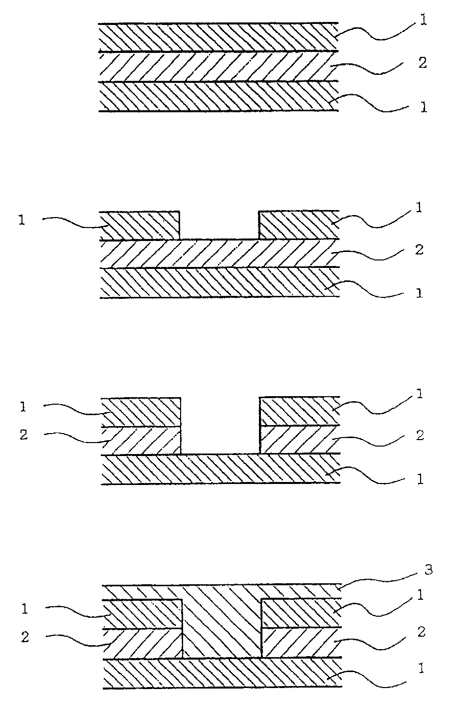
图2A至2D为示出根据本发明形成过孔的方法的一示例的解释性视图;2A to 2D are explanatory views showing an example of a method of forming a via hole according to the present invention;
图3A至3E为示出根据本发明形成过孔的方法的另一示例的解释性视图;3A to 3E are explanatory views showing another example of a method of forming a via hole according to the present invention;
图4A至4F′为示出根据本发明形成过孔的方法的再一示例的解释性视图。4A to 4F' are explanatory views showing still another example of a method of forming a via hole according to the present invention.
具体实施方式Detailed ways
下文参考附图适当地描述本发明,但是本发明并不限于在附图中所示的实施模式。以如下的顺序进行描述,即在描述根据本发明的柔性接线板的构造(比如材料、形状等)之前,描述作为本发明的一种特征的形成过孔的紫外线激光器。The present invention is suitably described below with reference to the accompanying drawings, but the present invention is not limited to the embodiment modes shown in the accompanying drawings. The description will be made in the order that the ultraviolet laser for forming a via hole as a feature of the present invention is described before describing the configuration (such as material, shape, etc.) of the flexible wiring board according to the present invention.
在本发明中使用波长在200至400纳米的范围(优选从240纳米至360纳米的范围)内的紫外线激光束来形成过孔。以具有如下的能量密度的紫外线激光束照射在柔性接线板中的导电体层和电绝缘层二者以在这两个层中形成开口,由此在柔性接线板中形成过孔。作为紫外线激光束,可以使用公知的激光束比如Nd:YAG激光器的三次谐波激光束(波长:355纳米)、受激准分子激光器(XeF)的激光束(波长:351纳米)或者受激准分子激光器(XrF)的激光束(波长:249纳米)。Vias are formed in the present invention using an ultraviolet laser beam with a wavelength in the range of 200 to 400 nm, preferably in the range from 240 nm to 360 nm. Both the conductor layer and the electrical insulating layer in the flexible wiring board were irradiated with an ultraviolet laser beam having an energy density as follows to form openings in both layers, thereby forming via holes in the flexible wiring board. As the ultraviolet laser beam, a well-known laser beam such as a third harmonic laser beam (wavelength: 355 nm) of a Nd:YAG laser, a laser beam (wavelength: 351 nm) of an excimer laser (XeF) or an excimer laser beam (wavelength: 351 nm) can be used. Laser beam (wavelength: 249 nm) of a molecular laser (XrF).
将参考图1A至1D描述所施加的紫外线激光束的能量。图1A至1D是说明在本发明中使用的紫外线激光束的辐射范围和能量密度的示例的典型视图。适合于处理在柔性接线板中的导电体层的紫外线激光束的辐射选择成使其能量密度(图1A和1B)高于用于处理电绝缘层的紫外线激光束的能量密度(图1C和1D)。优选的是,前者的能量密度选择成比后者的能量密度高0.1至20J/cm2的值。特别优选的是,前者的能量密度选择成比后者的能量密度高3至8.5J/cm2的值。在一般的激光束发生器中,通过调整施加到激光束源的电压和激光束的辐射尺寸容易控制这种能量密度。具体地说,用于处理导电体层的激光束的能量密度优选在从5至20J/cm2的范围,特别优选的是在从6至10J/cm2的范围,而用于处理电绝缘层的激光束的能量密度优选在从0.05至5J/cm2的范围,特别优选的是在从1.5至3J/cm2的范围。此外,优选的是,给要处理的目标表面上施加具有均匀的能量密度的激光束。这就是说,使用具有在图1B中所示的能量密度的激光束而不是具有在图1A中所示的能量密度的激光束来处理导电体层,而使用具有在图1D中所示的能量密度的激光束而不是具有在图1C中所示的能量密度的激光束来处理电绝缘层。为了获得在图1B和1D中所示的激光束,可以使用公知的波束成形光学系统,如微透镜阵列或屏蔽的投影系统。The energy of the applied ultraviolet laser beam will be described with reference to FIGS. 1A to 1D . 1A to 1D are typical views illustrating examples of radiation ranges and energy densities of ultraviolet laser beams used in the present invention. The irradiation of the ultraviolet laser beam suitable for processing the electrical conductor layer in the flexible wiring board is selected so that its energy density (Fig. ). Preferably, the energy density of the former is selected to be a value 0.1 to 20 J/cm 2 higher than the energy density of the latter. Particularly preferably, the energy density of the former is chosen to be 3 to 8.5 J/cm 2 higher than the energy density of the latter. In a general laser beam generator, such energy density is easily controlled by adjusting the voltage applied to the laser beam source and the radiation size of the laser beam. Specifically, the energy density of the laser beam used to process the electrical conductor layer is preferably in the range from 5 to 20 J/cm 2 , particularly preferably in the range from 6 to 10 J/cm 2 , while for the treatment of the electrically insulating layer The energy density of the laser beam is preferably in the range from 0.05 to 5 J/cm 2 , particularly preferably in the range from 1.5 to 3 J/cm 2 . Furthermore, it is preferable to apply a laser beam having a uniform energy density to the target surface to be processed. That is to say, the conductor layer is treated with a laser beam having the energy density shown in FIG. 1B instead of the laser beam having the energy density shown in FIG. Density of the laser beam instead of the laser beam having the energy density shown in FIG. 1C is used to treat the electrically insulating layer. To obtain the laser beams shown in FIGS. 1B and 1D , known beam-shaping optical systems such as microlens arrays or shielded projection systems can be used.
在施加到导电体层上的紫外线激光束的能量密度选择为较高时,可以防止在所处理的孔的周边产生突起并且能够缩短处理时间。在另一方面,在施加到电绝缘层上的紫外线激光束的能量密度选择为较低时,可以抑制过量的紫外线激光束辐射,因此可以减少热量的产生。结果,可以抑制对导电体层的周边和电绝缘层的周边的损害。此外,还可以抑制由热量引起的中间层脱落现象。因此,可以形成在工艺质量方面很好的加工孔,并抑制了突起的产生。良好工艺质量的加工孔可以防止在后续工艺中的不一致性,如在电镀工艺中的不均匀电沉积。这对于在柔性接线板中致密地形成精细图案非常有益。When the energy density of the ultraviolet laser beam applied to the conductor layer is selected to be high, it is possible to prevent protrusions from being generated at the periphery of the processed hole and to shorten the processing time. On the other hand, when the energy density of the ultraviolet laser beam applied to the electrical insulating layer is selected to be low, excessive ultraviolet laser beam radiation can be suppressed, and thus heat generation can be reduced. As a result, damage to the periphery of the conductor layer and the periphery of the electrical insulating layer can be suppressed. In addition, it is also possible to suppress the peeling phenomenon of the interlayer caused by heat. Therefore, a processed hole excellent in process quality can be formed, and the occurrence of protrusions is suppressed. Holes with good process quality can prevent inconsistencies in subsequent processes, such as uneven electrodeposition in electroplating processes. This is very beneficial for densely forming fine patterns in flexible wiring boards.
下文参考图2A至2D、图3至3E和图4A至4F′描述根据本发明的柔性接线板。图2A至2D、图3至3E和图4A至4F′为根据本发明的形成过孔的方法的示例的解释性视图。根据本发明的柔性接线板具有至少一种这样的结构,其中,作为预定电路图案的两个导电体层1设置在电绝缘层2的相对的表面上并且通过过孔彼此电连接。A flexible wiring board according to the present invention is described below with reference to FIGS. 2A to 2D , FIGS. 3 to 3E and FIGS. 4A to 4F'. 2A to 2D, 3 to 3E, and 4A to 4F' are explanatory views of an example of a method of forming a via hole according to the present invention. The flexible wiring board according to the present invention has at least one structure in which two
柔性接线板的最简单的模式是所谓的双面电路板,其中,导电体层1的电路图案形成在电绝缘层2的相对的表面上,如图2A至2D所示。在此所使用的概念“柔性接线板”包括例如五层结构的电路板,在这种五层结构中,导电体层1和电绝缘层2如图4A至4F′所示交替层叠。本发明的范围进一步包括具有两个或多个电绝缘层2的柔性接线板(未示出)和具有作为最外层的电绝缘层2而不是导电体层1的柔性接线板(未示出)。The simplest mode of a flexible wiring board is a so-called double-sided circuit board in which a circuit pattern of a
在本发明中使用的术语“过孔”与在本领域技术人员通常使用的意义相同。即,术语“过孔”意味着在柔性接线板中电连接通过至少一个电绝缘层2绝缘的多个导电体层1的导电通道。过孔可以设置成如图2D和4E′所示以导电金属填充的非通孔结构,或可以设置成如图3E和4F′所示电镀过孔的侧壁表面的结构。如下的结构也都属于过孔的范畴,只要该结构可以起导电通道的作用,这些结构有:比如电镀非通孔的侧壁表面的结构(未示)的任何其他结构,或者通过导电的方法而不是电镀,如应用导电膏所形成的结构。The term "via hole" used in the present invention has the same meaning as those generally used by those skilled in the art. That is, the term "via hole" means a conductive path that electrically connects a plurality of
对导电体层1的材料并没有特别的限制,只要该材料能够一般地用于柔性接线板的导电体层。例如,诸如铜、金、不锈钢或镍或他们合金的金属的金属箔都可以用作该材料。特别是,考虑到弹性、加工性能、电特性、成本等优选的是铜箔或铜合金箔。The material of the
对电绝缘层2的材料并没有特别的限制,只要该材料能够一般地用于柔性接线板的电绝缘层。例如,聚对苯二甲酸乙二醇酯、聚萘二甲酸乙二酯或聚酰亚胺都可以用作该材料。特别是,考虑到耐热性优选聚酰亚胺。There is no particular limitation on the material of the electrical insulating
参考图2A至2D描述作为本发明的第一实施例的在柔性接线板(图2A)中形成非通孔之后形成过孔的方法,该柔性接线板具有通过电绝缘层2彼此电绝缘的两个导电体层1。首先,以具有适合于处理导电体层1中的一个层的能量密度(即,优选在从5至20J/cm2的范围,特别优选的是在从6至10J/cm2的范围)的紫外线激光束照射在图2A中所示的柔性接线板上。因此,获得了如在图2B中所示的具有形成在作为第一层的导电体层1中的孔的结构。然后,以适合于处理电绝缘层2的能量密度(即,优选在从0.05至5J/cm2的范围,特别优选的是在从1.5至3J/cm2的范围)的紫外线激光束照射在图2B中所示的结构。因此,获得了如在图2C中所示的具有形成在作为第二层的电绝缘层2中的孔的结构。A method of forming a via hole after forming a non-through hole in a flexible wiring board ( FIG. 2A ) having two wires electrically insulated from each other by an electrical insulating
图2C中所示的柔性接线板(即,具有通过作为第三层的导电体层1阻塞的非通孔的结构)进行电镀工艺等以便完整填充该非通孔。因此,获得了如在图2D中所示的具有以导电金属填充的过孔的柔性接线板。The flexible wiring board shown in FIG. 2C (ie, a structure having a non-through hole blocked by the
虽然本实施例通过举例的方式已经示出了通过电镀工艺以导电金属填充的非通孔的情况,但是电镀方法和种类并不受到特别的限制。本领域技术人员所公知的方法都可以用作电镀的方法。作为电镀的类型,例如镀金、镀铜、镀镍或焊接镀都可以选择。电镀或无电电镀(electroless plating)都可以作为电镀方法。Although the present embodiment has shown the case of a non-through hole filled with a conductive metal through an electroplating process by way of example, the electroplating method and type are not particularly limited. Any method known to those skilled in the art can be used as the electroplating method. As the type of plating, for example gold plating, copper plating, nickel plating or solder plating can be selected. Electroplating or electroless plating (electroless plating) can be used as the plating method.
在形成了如图2D所示的过孔之后,在以公知的方法比如蚀刻法在通过电绝缘层2彼此绝缘的两个导电体层1中形成所需的电路图案时,可以获得根据本发明的柔性接线板。可替换的是,在形成孔之前或在实施电镀工艺之前可以形成这种电路图案。After forming the via hole as shown in FIG. 2D , when a desired circuit pattern is formed in two
参考图3A至3E描述作为本发明的第二实施例的在柔性接线板(图3A)中形成通孔之后形成过孔的方法,该柔性接线板具有由电绝缘层2彼此绝缘的两个导电体层1。首先,从在图3A中所示的结构以与第一实施例相同的方式获得如图3C所示的结构,该结构具有形成在作为第一层的导电体层1和作为第二层的电绝缘层2中的孔。然后,以具有适合于处理导电体层1的能量密度的紫外线激光束照射在图3C中所示的结构,由此在作为第三层的导电体层1中形成加工孔。因此,获得如在图3D中所示的通孔。然后,以与第一实施例相同的方式对通孔的侧壁表面进行电镀处理。因此,可以获得如在图3E所示的过孔。此外,以与第一实施例相同的方式在导电体层1中形成所需的电路。因此,可以获得根据本发明的柔性接线板。A method of forming a via hole after forming a via hole in a flexible wiring board ( FIG. 3A ) having two conductive wires insulated from each other by an electrical insulating
根据本发明的柔性接线板不必具有如图2A至2D和图3A至3E所示的三层结构。即,柔性接线板可以具有如下的五层结构:在该结构中导电体层1和电绝缘层2如图4A至4F′所示交错层叠,或者该柔性接线板可以具有更多的层的结构(未示)。在柔性接线板具有如在图4A至4F′所示的五层结构时,如果通过具有分别在这些范围中的能量密度的紫外线激光束处理导电体层和电绝缘层并进行电镀,则可以形成具有如在图4E′中所示的结构的过孔(通过在图4E的阶段中进行电镀)或者可以形成具有如在图4F′所示的结构的过孔(通过电镀如在图4F中所示的通孔的壁表面)。The flexible wiring board according to the present invention does not necessarily have a three-layer structure as shown in FIGS. 2A to 2D and FIGS. 3A to 3E. That is, the flexible wiring board may have a five-layer structure in which conductor layers 1 and electrical insulating
示例example
下文参考在本发明的实施例的描述中使用的附图(图2A至2D、图3A至3E和图4A至4F′)描述本发明的示例,但是本发明并不限于该示例。在本发明中使用的紫外线激光束是Nd:YAG激光器的三次谐波,它是一种具有355纳米的波长的激光束。通过调整激光器的“功率”和“波束尺寸”设定辐射的能量密度。通过改变激光加工装置的焦点的变化调整“波束尺寸”。通过微透镜阵列调整激光束的能量分布。An example of the present invention is described below with reference to drawings ( FIGS. 2A to 2D , FIGS. 3A to 3E , and FIGS. 4A to 4F ′) used in descriptions of embodiments of the present invention, but the present invention is not limited to this example. The ultraviolet laser beam used in the present invention is the third harmonic of Nd:YAG laser, which is a laser beam with a wavelength of 355 nm. The energy density of the radiation is set by adjusting the "power" and "beam size" of the laser. Adjust the "beam size" by changing the focal point of the laser processing device. The energy distribution of the laser beam is adjusted by a microlens array.
(示例1)(Example 1)
在本示例中,使用如图2A所示的柔性接线板。在该柔性接线板中,作为第一和第三层的导电体层1每层都由9微米厚的铜箔制成,作为在两个导电体层1之间的第二层的电绝缘层2由25微米厚的聚酰亚胺制成。In this example, a flexible wiring board as shown in Fig. 2A is used. In this flexible wiring board, the conductor layers 1 as the first and third layers are each made of 9 micron thick copper foil as the electrical insulating layer of the second layer between the two
首先,分别将紫外线激光束的功率、频率和波束尺寸分别设定为0.25瓦、4千赫兹和φ30微米,即将紫外线激光束的能量密度设定在8.8J/cm2以处理作为第一层的导电体层1。在这种情况下,通过该紫外线激光束的辐射处理导电体层1持续85毫秒。因此,在导电体层1中形成如在图2B中所示的孔。然后,分别将紫外线激光束的功率、频率和波束尺寸分别设定为0.5瓦、7.142千赫兹和φ55微米,即将紫外线激光束的能量密度设定在2.9J/cm2以处理作为第二层的电绝缘层2。在这种情况下,通过该紫外线激光束的辐射处理电绝缘层2持续85毫秒。因此,在电绝缘层2中形成如在图2C中所示的孔。First, the power, frequency and beam size of the ultraviolet laser beam were respectively set to 0.25 watts, 4 kHz and φ30 microns, that is, the energy density of the ultraviolet laser beam was set at 8.8J/cm 2 to treat as the first
对在图2C所示的结构中的非通孔进行电解铜电镀以便在导电体层1上的淀积层厚10微米。因此,获得具有如在图2D中所示的电连接的柔性接线板。在该柔性接线板中,在加工孔的周边上既不存在突起,在电镀的过程中也不存在不均匀沉淀的缺陷。Electrolytic copper plating was performed on the non-through holes in the structure shown in FIG. 2C so that the deposited layer thickness on the
(示例2)(Example 2)
在本实例中使用的柔性接线板与在实例1中使用的柔性接线板相同。参考图3A至3E描述这种实例。The flexible wiring board used in this example is the same as that used in Example 1. Such an example is described with reference to FIGS. 3A to 3E .
以与在实例1中相同的方式实施在图3A至3E中的处理。在本实例中,以紫外线激光束进一步照射作为第三层的导电体层1,由此形成如图3D所示的通孔。处理第三层的条件与处理作为第一层的导电体层1的条件相同。The processing in FIGS. 3A to 3E is carried out in the same manner as in Example 1. In this example, the
在处理通孔之后,施加电解镀铜以使在导电体层1上淀积层厚10微米。因此,获得了如在图3E中所示的具有电连接的柔性接线板。在柔性接线板中的加工孔的周边上也既不存在突起,在电镀的过程中也不存在不均匀沉淀的缺陷。After processing the vias, electrolytic copper plating was applied so that a layer thickness of 10 microns was deposited on the
(示例3)(Example 3)
参考图4A至4F′描述本实例。在本示例中,使用在图4A中所示的柔性接线板。在该柔性接线板中,作为第一、第三和第五层的导电体层1的每层都由9微米厚的铜箔制成,而作为第二和第四层的电绝缘层2每层都由25微米厚的聚酰亚胺制成。This example is described with reference to FIGS. 4A to 4F'. In this example, the flexible wiring board shown in Fig. 4A is used. In this flexible wiring board, each of the
即使在要层叠的层的数量不是3而是5的情况下,也能够根据本发明处理过孔而不存在任何问题。首先,通过每次两层相间地将在一定范围的能量密度的紫外线激光束施加到导电体层1的四个层上和两个电绝缘层2上来实施从在图4A中所示的柔性接线板到在图4E中所示的结构的处理。因此产生了两个柔性接线板。两个柔性接线板中的一个用于准备制造在图4E′中所示的过孔。另一个用于准备制造在图4F′中所示的过孔。对两个柔性接线板进行如下的处理。Even in the case where the number of layers to be laminated is not 3 but 5, vias can be processed according to the present invention without any problem. First, the flexible wiring shown in FIG. Plate processing into the configuration shown in Figure 4E. Thus two flexible wiring boards are produced. One of the two flexible wiring boards is used to prepare the vias shown in FIG. 4E'. The other is used in preparation for fabrication of the vias shown in Figure 4F'. Do the following for the two flexible wiring boards.
在前一种情况下,对在图4E中所示的状态的柔性接线板进行电解镀铜以使在导电体层1上的淀积层厚10微米。因此,获得了如图4E′所示具有过孔的柔性接线板。在柔性接线板中的加工孔的周边上也既不存在突起,在电镀的过程中也不存在不均匀沉淀的缺陷。In the former case, electrolytic copper plating was performed on the flexible wiring board in the state shown in FIG. 4E so that the deposited layer on the
在另一方面,在后一种情况下,以紫外线激光束进一步照射在图4E所示的状态的柔性接线板中的作为第五层的导电体层1。因此,形成了如图4F中所示的通孔。处理第五层的条件与处理作为第一和第三层的导电体层1的条件相同。然后,对柔性接线板进行电解电镀以使在导电体层1上的淀积层厚10微米。因此,获得了如图4F′所示具有过孔的柔性接线板。在柔性接线板中的加工孔的周边上也既不存在突起,在电镀的过程中也不存在不均匀沉淀的缺陷。On the other hand, in the latter case, the
(对比例1)(comparative example 1)
实施与在示例1中处理加工孔相同的处理,同时将所施加的紫外线激光束的能量密度一直设定在8.8J/cm2(也用于处理电绝缘层2)。The same treatment as in the treatment of the processed hole in Example 1 was performed while always setting the energy density of the applied ultraviolet laser beam at 8.8 J/cm 2 (also used for the treatment of the electrical insulating layer 2).
在这种情况下,在图2C中所示的阶段中产生了损害,因此在作为第三层的导电体层1中观察到了波纹。如果形成了这种加工孔,则可以判定由于在电镀过程中产生的裂纹造成了电连接失败。In this case, damage was generated in the stage shown in FIG. 2C , so ripples were observed in the
(对比例2)(comparative example 2)
实施与在实例1中处理加工孔相同的处理,同时将所施加的紫外线激光束的能量密度一直设定在2.9J/cm2(也用于处理导电体层1)。在这种情况下,处理导电体层1所需的时间变得较长(在实例1中要求85毫秒的处理时间,而在比较实例中要求2秒的处理时间)。此外,在作为第一层的导电体层1的加工孔的周边中观察到了突起。The same treatment as in Example 1 for processing the hole was carried out while always setting the energy density of the applied ultraviolet laser beam at 2.9 J/cm 2 (also used for the treatment of the conductor layer 1). In this case, the time required to process the
(对比例3)(comparative example 3)
实施与在实例2中处理加工孔相同的处理,同时将所施加的紫外线激光束的能量密度一直设定在8.8J/cm2(也用于处理电绝缘层2)。The same treatment as in the treatment of the processed hole in Example 2 was carried out while always setting the energy density of the applied ultraviolet laser beam at 8.8 J/cm 2 (also for the treatment of the electrical insulating layer 2).
在这种情况下,因为以8.8J/cm2的能量密度进行处理的缘故,所以在图3D所示的阶段中在电绝缘层2中产生了微裂纹。结果,在电镀过程中产生了桶状裂纹(在加工孔的侧表面上由不充分电镀引起的断裂状态)。如果使用这种柔性接线板,则担心在后续处理中可能会失效。In this case, because of the treatment at an energy density of 8.8 J/cm 2 , microcracks were generated in the electrical insulating
(对比例4)(comparative example 4)
实施与在实例2中处理加工孔相同的处理,同时将所施加的紫外线激光束的能量密度一直设定在2.9J/cm2(也用于处理导电体层1)。The same treatment as in Example 2 for processing the processing hole was carried out while always setting the energy density of the applied ultraviolet laser beam at 2.9 J/cm 2 (also used for the treatment of the conductor layer 1).
在这种情况下,与比较实例2一样处理导电体层1所需的时间变得较长。此外,由于在处理作为第三层的导电体层1时在孔的里面积累了热量的原因,在电绝缘层2中产生了微裂纹。如果形成了这种通孔,则引起的问题是发生桶状裂纹由此在电镀之后降低过孔的可靠性。In this case, the time required to process the
在比较实例1至4中所描述的条件下以紫外线激光束照射如图4A至4F′所示的具有5层结构的柔性接线板时,根据过孔的形状和紫外线激光束的能量密度可以确认产生了在比较实例1至4中所描述的失效。When a flexible wiring board having a 5-layer structure as shown in FIGS. The failures described in Comparative Examples 1 to 4 occurred.
根据本发明,可以减少为形成过孔所施加的过量热能。因此,可以减小在现有技术的过孔中产生的问题,因此可以提高质量。这样,可以结合过孔的质量的提高和由于使用紫外线激光束带来的精密而又精确的加工性能而在柔性接线板中致密地实现精细构图。此外,可以预计到因过孔所带来的电连接的可靠性的提高。可以预计的是这种柔性接线板进一步减小了电子设备的重量和厚度,并且进一步增加了电子设备的密度。According to the present invention, it is possible to reduce excessive thermal energy applied for forming via holes. Therefore, the problems generated in the vias of the related art can be reduced, and thus the quality can be improved. In this way, fine patterning can be densely realized in a flexible wiring board in combination with improvement in the quality of via holes and fine and precise processability due to the use of ultraviolet laser beams. In addition, improvement in reliability of electrical connection due to via holes can be expected. It is expected that such a flexible wiring board further reduces the weight and thickness of the electronic equipment, and further increases the density of the electronic equipment.
Claims (5)
Applications Claiming Priority (3)
| Application Number | Priority Date | Filing Date | Title |
|---|---|---|---|
| JP2001294956A JP2003101188A (en) | 2001-09-26 | 2001-09-26 | Method for forming via hole, flexible wiring board using the same, and method for manufacturing the same |
| JP294956/01 | 2001-09-26 | ||
| JP294956/2001 | 2001-09-26 |
Publications (2)
| Publication Number | Publication Date |
|---|---|
| CN1409587A CN1409587A (en) | 2003-04-09 |
| CN1240259C true CN1240259C (en) | 2006-02-01 |
Family
ID=19116468
Family Applications (1)
| Application Number | Title | Priority Date | Filing Date |
|---|---|---|---|
| CNB021323712A Expired - Fee Related CN1240259C (en) | 2001-09-26 | 2002-09-24 | Method for forming holes, using flexible connection board formed thereof and its producing method |
Country Status (4)
| Country | Link |
|---|---|
| US (1) | US6642478B2 (en) |
| JP (1) | JP2003101188A (en) |
| KR (1) | KR100538604B1 (en) |
| CN (1) | CN1240259C (en) |
Families Citing this family (15)
| Publication number | Priority date | Publication date | Assignee | Title |
|---|---|---|---|---|
| JP2005116868A (en) * | 2003-10-09 | 2005-04-28 | Nitto Denko Corp | Method for manufacturing multilayer printed circuit board |
| JP2005342749A (en) * | 2004-06-01 | 2005-12-15 | Hitachi Via Mechanics Ltd | Laser processing method |
| KR100737094B1 (en) * | 2005-11-14 | 2007-07-06 | 엘지이노텍 주식회사 | Through Hole Printing Process |
| US7605343B2 (en) * | 2006-05-24 | 2009-10-20 | Electro Scientific Industries, Inc. | Micromachining with short-pulsed, solid-state UV laser |
| JP5162977B2 (en) * | 2006-07-28 | 2013-03-13 | 日立化成株式会社 | Laser drilling method |
| KR100824964B1 (en) * | 2006-12-26 | 2008-04-28 | 주식회사 코윈디에스티 | Metal thin film forming apparatus and method using laser |
| US20090004403A1 (en) * | 2007-06-29 | 2009-01-01 | Yonggang Li | Method of Providing Patterned Embedded Conducive Layer Using Laser Aided Etching of Dielectric Build-Up Layer |
| CN101477859B (en) * | 2009-01-16 | 2011-11-30 | 上海科特高分子材料有限公司 | Novel surface mounting type thermistor and manufacturing method thereof |
| JP4883203B2 (en) * | 2009-07-01 | 2012-02-22 | 株式会社テラミクロス | Manufacturing method of semiconductor device |
| JP5233929B2 (en) * | 2009-09-14 | 2013-07-10 | 日立電線株式会社 | Method for manufacturing printed wiring board |
| JP5935101B2 (en) * | 2011-09-16 | 2016-06-15 | 株式会社ブイ・テクノロジー | Thin film pattern forming method |
| KR102078888B1 (en) | 2011-09-16 | 2020-02-19 | 브이 테크놀로지 씨오. 엘티디 | Vapor-deposition mask, vapor-deposition mask manufacturing method, and thin-film pattern forming method |
| KR102356809B1 (en) * | 2014-12-26 | 2022-01-28 | 삼성전기주식회사 | Printed circuit board and method of manufacturing the same |
| CN104703397B (en) * | 2015-03-27 | 2018-03-09 | 大族激光科技产业集团股份有限公司 | A kind of method of flexible circuitry board blind hole processing |
| JP7452092B2 (en) * | 2020-02-27 | 2024-03-19 | 株式会社豊田中央研究所 | Laser processing equipment, laser processing method, and control method for laser processing equipment |
Family Cites Families (2)
| Publication number | Priority date | Publication date | Assignee | Title |
|---|---|---|---|---|
| EP0539741B1 (en) * | 1991-09-30 | 2003-01-15 | Canon Kabushiki Kaisha | Anodic bonding process with light irradiation |
| JP3756723B2 (en) * | 1999-07-27 | 2006-03-15 | 松下電工株式会社 | Processing method of printed wiring board |
-
2001
- 2001-09-26 JP JP2001294956A patent/JP2003101188A/en active Pending
-
2002
- 2002-09-23 US US10/251,820 patent/US6642478B2/en not_active Expired - Fee Related
- 2002-09-24 CN CNB021323712A patent/CN1240259C/en not_active Expired - Fee Related
- 2002-09-26 KR KR10-2002-0058421A patent/KR100538604B1/en not_active Expired - Fee Related
Also Published As
| Publication number | Publication date |
|---|---|
| CN1409587A (en) | 2003-04-09 |
| US20030057193A1 (en) | 2003-03-27 |
| US6642478B2 (en) | 2003-11-04 |
| JP2003101188A (en) | 2003-04-04 |
| KR100538604B1 (en) | 2005-12-22 |
| KR20030027750A (en) | 2003-04-07 |
Similar Documents
| Publication | Publication Date | Title |
|---|---|---|
| CN1240259C (en) | Method for forming holes, using flexible connection board formed thereof and its producing method | |
| JP3983146B2 (en) | Manufacturing method of multilayer wiring board | |
| CN1458815A (en) | Metal core base plate and its producing process | |
| CN1798479A (en) | Printed circuit board including embedded chips and method of fabricating the same | |
| CN1392611A (en) | Semiconductor device and its producing method | |
| CN1189760A (en) | Printed Circuit Boards and Electronic Components | |
| JP2005501415A (en) | Interconnect module with reduced power distribution impedance | |
| CN101516165A (en) | Printed wiring board and manufacturing method therefor | |
| CN1829420A (en) | Printed circuit board with embedded capacitors therein and manufacturing process thereof | |
| CN1520704A (en) | Core board and multilayer circuit board using core board | |
| KR20130037209A (en) | Wiring board production method | |
| CN1825581A (en) | Printed circuit board, flip chip ball grid array board and method of fabricating the same | |
| JPH0936522A (en) | Circuit forming method for printed wiring board | |
| KR101393892B1 (en) | Wiring board and manufacturing process for same | |
| TW201206277A (en) | Method of fabricating wiring board | |
| US9497853B2 (en) | Printed circuit board and method for manufacturing the same | |
| CN1620232A (en) | A wiring substrate and its manufacturing method | |
| JP4734723B2 (en) | Manufacturing method of multilayer wiring board using coaxial via hole | |
| US5034569A (en) | Multilayer interconnection circuit board | |
| JP2000216513A (en) | Wiring board and manufacturing method using the same | |
| CN1620230A (en) | A method of manufacturing a wiring board | |
| JP2004186354A (en) | Method of manufacturing multilayer wiring board | |
| KR20040108817A (en) | Laser beam machining method | |
| JP4802402B2 (en) | High-density multilayer build-up wiring board and manufacturing method thereof | |
| JP2002280743A (en) | Multilayer printed wiring board and its manufacturing method |
Legal Events
| Date | Code | Title | Description |
|---|---|---|---|
| C06 | Publication | ||
| PB01 | Publication | ||
| C10 | Entry into substantive examination | ||
| SE01 | Entry into force of request for substantive examination | ||
| C14 | Grant of patent or utility model | ||
| GR01 | Patent grant | ||
| C17 | Cessation of patent right | ||
| CF01 | Termination of patent right due to non-payment of annual fee |
Granted publication date: 20060201 Termination date: 20110924 |