CN116325193A - Unit pixel with light-emitting element, manufacturing method of the unit pixel, and display device with the unit pixel - Google Patents
Unit pixel with light-emitting element, manufacturing method of the unit pixel, and display device with the unit pixel Download PDFInfo
- Publication number
- CN116325193A CN116325193A CN202180069843.5A CN202180069843A CN116325193A CN 116325193 A CN116325193 A CN 116325193A CN 202180069843 A CN202180069843 A CN 202180069843A CN 116325193 A CN116325193 A CN 116325193A
- Authority
- CN
- China
- Prior art keywords
- layer
- light
- blocking layer
- light emitting
- light blocking
- Prior art date
- Legal status (The legal status is an assumption and is not a legal conclusion. Google has not performed a legal analysis and makes no representation as to the accuracy of the status listed.)
- Pending
Links
Images


Classifications
-
- H—ELECTRICITY
- H10—SEMICONDUCTOR DEVICES; ELECTRIC SOLID-STATE DEVICES NOT OTHERWISE PROVIDED FOR
- H10W—GENERIC PACKAGES, INTERCONNECTIONS, CONNECTORS OR OTHER CONSTRUCTIONAL DETAILS OF DEVICES COVERED BY CLASS H10
- H10W90/00—Package configurations
-
- H—ELECTRICITY
- H10—SEMICONDUCTOR DEVICES; ELECTRIC SOLID-STATE DEVICES NOT OTHERWISE PROVIDED FOR
- H10H—INORGANIC LIGHT-EMITTING SEMICONDUCTOR DEVICES HAVING POTENTIAL BARRIERS
- H10H20/00—Individual inorganic light-emitting semiconductor devices having potential barriers, e.g. light-emitting diodes [LED]
- H10H20/80—Constructional details
- H10H20/81—Bodies
- H10H20/814—Bodies having reflecting means, e.g. semiconductor Bragg reflectors
-
- H—ELECTRICITY
- H10—SEMICONDUCTOR DEVICES; ELECTRIC SOLID-STATE DEVICES NOT OTHERWISE PROVIDED FOR
- H10H—INORGANIC LIGHT-EMITTING SEMICONDUCTOR DEVICES HAVING POTENTIAL BARRIERS
- H10H20/00—Individual inorganic light-emitting semiconductor devices having potential barriers, e.g. light-emitting diodes [LED]
- H10H20/80—Constructional details
- H10H20/84—Coatings, e.g. passivation layers or antireflective coatings
- H10H20/841—Reflective coatings, e.g. dielectric Bragg reflectors
-
- H—ELECTRICITY
- H10—SEMICONDUCTOR DEVICES; ELECTRIC SOLID-STATE DEVICES NOT OTHERWISE PROVIDED FOR
- H10H—INORGANIC LIGHT-EMITTING SEMICONDUCTOR DEVICES HAVING POTENTIAL BARRIERS
- H10H20/00—Individual inorganic light-emitting semiconductor devices having potential barriers, e.g. light-emitting diodes [LED]
- H10H20/80—Constructional details
- H10H20/85—Packages
- H10H20/855—Optical field-shaping means, e.g. lenses
-
- H—ELECTRICITY
- H10—SEMICONDUCTOR DEVICES; ELECTRIC SOLID-STATE DEVICES NOT OTHERWISE PROVIDED FOR
- H10H—INORGANIC LIGHT-EMITTING SEMICONDUCTOR DEVICES HAVING POTENTIAL BARRIERS
- H10H20/00—Individual inorganic light-emitting semiconductor devices having potential barriers, e.g. light-emitting diodes [LED]
- H10H20/80—Constructional details
- H10H20/85—Packages
- H10H20/855—Optical field-shaping means, e.g. lenses
- H10H20/856—Reflecting means
-
- H—ELECTRICITY
- H10—SEMICONDUCTOR DEVICES; ELECTRIC SOLID-STATE DEVICES NOT OTHERWISE PROVIDED FOR
- H10H—INORGANIC LIGHT-EMITTING SEMICONDUCTOR DEVICES HAVING POTENTIAL BARRIERS
- H10H20/00—Individual inorganic light-emitting semiconductor devices having potential barriers, e.g. light-emitting diodes [LED]
- H10H20/80—Constructional details
- H10H20/85—Packages
- H10H20/857—Interconnections, e.g. lead-frames, bond wires or solder balls
-
- H—ELECTRICITY
- H10—SEMICONDUCTOR DEVICES; ELECTRIC SOLID-STATE DEVICES NOT OTHERWISE PROVIDED FOR
- H10H—INORGANIC LIGHT-EMITTING SEMICONDUCTOR DEVICES HAVING POTENTIAL BARRIERS
- H10H20/00—Individual inorganic light-emitting semiconductor devices having potential barriers, e.g. light-emitting diodes [LED]
- H10H20/01—Manufacture or treatment
- H10H20/036—Manufacture or treatment of packages
- H10H20/0363—Manufacture or treatment of packages of optical field-shaping means
-
- H—ELECTRICITY
- H10—SEMICONDUCTOR DEVICES; ELECTRIC SOLID-STATE DEVICES NOT OTHERWISE PROVIDED FOR
- H10H—INORGANIC LIGHT-EMITTING SEMICONDUCTOR DEVICES HAVING POTENTIAL BARRIERS
- H10H20/00—Individual inorganic light-emitting semiconductor devices having potential barriers, e.g. light-emitting diodes [LED]
- H10H20/80—Constructional details
- H10H20/81—Bodies
- H10H20/819—Bodies characterised by their shape, e.g. curved or truncated substrates
- H10H20/82—Roughened surfaces, e.g. at the interface between epitaxial layers
-
- H—ELECTRICITY
- H10—SEMICONDUCTOR DEVICES; ELECTRIC SOLID-STATE DEVICES NOT OTHERWISE PROVIDED FOR
- H10H—INORGANIC LIGHT-EMITTING SEMICONDUCTOR DEVICES HAVING POTENTIAL BARRIERS
- H10H20/00—Individual inorganic light-emitting semiconductor devices having potential barriers, e.g. light-emitting diodes [LED]
- H10H20/80—Constructional details
- H10H20/83—Electrodes
- H10H20/831—Electrodes characterised by their shape
-
- H—ELECTRICITY
- H10—SEMICONDUCTOR DEVICES; ELECTRIC SOLID-STATE DEVICES NOT OTHERWISE PROVIDED FOR
- H10H—INORGANIC LIGHT-EMITTING SEMICONDUCTOR DEVICES HAVING POTENTIAL BARRIERS
- H10H20/00—Individual inorganic light-emitting semiconductor devices having potential barriers, e.g. light-emitting diodes [LED]
- H10H20/80—Constructional details
- H10H20/882—Scattering means
-
- H—ELECTRICITY
- H10—SEMICONDUCTOR DEVICES; ELECTRIC SOLID-STATE DEVICES NOT OTHERWISE PROVIDED FOR
- H10H—INORGANIC LIGHT-EMITTING SEMICONDUCTOR DEVICES HAVING POTENTIAL BARRIERS
- H10H29/00—Integrated devices, or assemblies of multiple devices, comprising at least one light-emitting semiconductor element covered by group H10H20/00
- H10H29/80—Constructional details
- H10H29/882—Scattering means
Landscapes
- Led Device Packages (AREA)
- Led Devices (AREA)
Abstract
提供了一种单元像素。根据一实施例的单元像素包括:透明基板;第一光阻断层,布置于所述透明基板上,并具有使光透射的窗;粘合层,覆盖所述第一光阻断层;多个发光元件,以整齐排列于所述窗的方式布置于所述粘合层上;以及第二光阻断层,覆盖所述发光元件的侧表面。
A unit pixel is provided. A unit pixel according to an embodiment includes: a transparent substrate; a first light blocking layer disposed on the transparent substrate and having a window for transmitting light; an adhesive layer covering the first light blocking layer; a light-emitting element arranged on the adhesive layer in a manner aligned with the window; and a second light-blocking layer covering side surfaces of the light-emitting element.
Description
技术领域technical field
示例性的实施例涉及一种具有发光元件的单元像素、该单元像素的制造方法及具有该单元像素的显示装置。Exemplary embodiments relate to a unit pixel having a light emitting element, a method of manufacturing the unit pixel, and a display device having the unit pixel.
背景技术Background technique
发光元件是利用作为无机光源的发光二极管的半导体元件,正广泛应用于诸如显示装置、车辆用灯具、一般照明之类的多种领域。发光二极管具有寿命长、耗电低、响应速度快的优点,因此正迅速代替现有光源。A light-emitting element is a semiconductor element using a light-emitting diode as an inorganic light source, and is widely used in various fields such as display devices, vehicle lamps, and general lighting. Light-emitting diodes have the advantages of long life, low power consumption, and fast response, so they are rapidly replacing existing light sources.
另外,现有的发光二极管在显示装置中主要用作背光光源,最近正在开发利用发光二极管来直接实现图像的显示装置。这种显示器也被称为微型LED显示器。In addition, conventional light-emitting diodes are mainly used as backlight sources in display devices, and recently, display devices that directly realize images using light-emitting diodes are being developed. Such displays are also known as Micro LED displays.
显示装置通常利用蓝色、绿色及红色的混合色来实现多样的颜色。显示装置包括多个像素以实现多样的图像,各个像素配备蓝色子像素、绿色子像素及红色子像素。通过这些子像素的颜色来确定特定像素的颜色,并且借由这些像素的组合来实现图像。Display devices usually utilize mixed colors of blue, green and red to achieve various colors. The display device includes a plurality of pixels to realize various images, and each pixel is equipped with blue sub-pixels, green sub-pixels and red sub-pixels. The color of a specific pixel is determined by the color of these sub-pixels, and an image is realized by the combination of these pixels.
在微型LED显示器的情况下,微型LED与各个子像素对应地排列在二维平面上,据此,需要在一个基板上布置大量的微型LED。然而,微型LED的尺寸非常小,例如200um以下,进而100um以下,非常小,因这种较小尺寸而发生多样的问题。尤其,难以处理较小尺寸的发光二极管,因此不容易在显示器用面板上直接贴装发光二极管。In the case of a micro LED display, micro LEDs are arranged on a two-dimensional plane corresponding to each sub-pixel, and accordingly, a large number of micro LEDs need to be arranged on one substrate. However, the size of the micro LED is very small, such as below 200um, and furthermore, it is very small below 100um, and various problems occur due to such a small size. In particular, since it is difficult to handle small-sized light-emitting diodes, it is not easy to directly mount light-emitting diodes on a display panel.
另外,相邻的子像素之间的光干涉使得难以实现高颜色再现性及高对比度。In addition, light interference between adjacent sub-pixels makes it difficult to achieve high color reproducibility and high contrast.
发明内容Contents of the invention
技术问题technical problem
示例性的实施例提供一种适合贴装于电路基板的单元像素及具有该单元像素的显示装置。Exemplary embodiments provide a unit pixel suitable for mounting on a circuit substrate and a display device having the unit pixel.
示例性的实施例提供一种可通过防止光干涉来实现高颜色再现性的单元像素及具有该单元像素的显示装置。Exemplary embodiments provide a unit pixel that can achieve high color reproducibility by preventing light interference and a display device having the same.
技术方案Technical solutions
示例性的实施例提供一种单元像素,该单元像素包括:透明基板;第一光阻断层,布置于所述透明基板上,并具有使光透射的窗;粘合层,覆盖所述第一光阻断层;多个发光元件,以整齐排列于所述窗的方式布置于所述粘合层上;以及第二光阻断层,覆盖所述发光元件的侧表面。Exemplary embodiments provide a unit pixel including: a transparent substrate; a first light-blocking layer disposed on the transparent substrate and having a window for transmitting light; an adhesive layer covering the first light-blocking layer. A light-blocking layer; a plurality of light-emitting elements arranged on the adhesive layer in a manner aligned with the window; and a second light-blocking layer covering side surfaces of the light-emitting elements.
示例性的实施例提供一种单元像素的制造方法,该方法包括如下步骤:准备透明基板;在所述透明基板上形成具有多个窗的第一光阻断层;形成覆盖所述第一光阻断层的粘合层;在所述粘合层上以对应于所述窗的方式安装发光元件;形成覆盖所述发光元件的侧表面的第二光阻断层。An exemplary embodiment provides a method for manufacturing a unit pixel. The method includes the following steps: preparing a transparent substrate; forming a first light blocking layer having a plurality of windows on the transparent substrate; an adhesive layer of a blocking layer; mounting a light emitting element on the adhesive layer in a manner corresponding to the window; forming a second light blocking layer covering a side surface of the light emitting element.
示例性的实施例提供一种显示装置,该显示装置包括:电路基板;以及单元像素,安装于所述电路基板上,其中,所述单元像素中的每一个包括:透明基板;第一光阻断层,布置于所述透明基板上,并具有使光透射的窗;粘合层,覆盖所述第一光阻断层;多个发光元件,以整齐排列于所述窗的方式布置于所述粘合层上;以及第二光阻断层,覆盖所述发光元件的侧表面。Exemplary embodiments provide a display device including: a circuit substrate; and unit pixels mounted on the circuit substrate, wherein each of the unit pixels includes: a transparent substrate; a first photoresist a fault layer arranged on the transparent substrate and having a window for transmitting light; an adhesive layer covering the first light blocking layer; a plurality of light emitting elements arranged on the window in a neatly arranged manner on the adhesive layer; and a second light blocking layer covering the side surface of the light emitting element.
附图说明Description of drawings
图1是用于说明根据一实施例的显示装置的示意性的平面图。FIG. 1 is a schematic plan view for explaining a display device according to an embodiment.
图2A是用于说明根据一实施例的发光元件的示意性的平面图。FIG. 2A is a schematic plan view for explaining a light emitting element according to an embodiment.
图2B是沿图2A的剖切线A-A'剖切的示意性的剖面图。FIG. 2B is a schematic cross-sectional view taken along line AA' of FIG. 2A .
图3A是用于说明根据一实施例的单元像素的示意性的平面图。FIG. 3A is a schematic plan view for explaining a unit pixel according to an embodiment.
图3B是沿图3A的剖切线B-B'剖切的示意性的剖面图。FIG. 3B is a schematic cross-sectional view taken along the section line BB' of FIG. 3A .
图3C是图3B的局部剖面图。FIG. 3C is a partial cross-sectional view of FIG. 3B.
图4A是用于说明根据一实施例的像素模块的示意性的平面图。FIG. 4A is a schematic plan view illustrating a pixel module according to an embodiment.
图4B是沿图4A的剖切线C-C'剖切的示意性的剖面图。FIG. 4B is a schematic cross-sectional view taken along line CC' of FIG. 4A .
图5是用于说明根据一实施例的单元像素的示意性的剖面图。FIG. 5 is a schematic cross-sectional view for explaining a unit pixel according to an embodiment.
图6是用于说明根据一实施例的单元像素的示意性的剖面图。FIG. 6 is a schematic cross-sectional view for explaining a unit pixel according to an embodiment.
图7A至图7F是用于说明根据一实施例的单元像素的制造方法的示意性的剖面图。7A to 7F are schematic cross-sectional views illustrating a method of manufacturing a unit pixel according to an embodiment.
具体实施方式Detailed ways
以下,参照附图详细说明本公开的实施例。以下介绍的实施例是为了将本公开的思想充分传递给本公开所属技术领域的普通技术人员而作为示例提供的。因此,本公开并不限于以下说明的实施例,其也可以具体化为其他形态。并且,在附图中,为了方便起见,构成要素的宽度、长度、厚度等可能被夸大表示。并且,在记载为一个构成要素位于另一构成要素的“上部”或“之上”的情况下,不仅包括各个部分位于另一部分的“紧邻的上部”或“之上”的情况,还包括在各个结构要素与另一结构要素之间夹设有其他构成要素的情况。在整个说明书中,相同的附图标记表示相同的构成要素。Hereinafter, embodiments of the present disclosure will be described in detail with reference to the drawings. The embodiments described below are provided as examples in order to fully convey the idea of the present disclosure to those of ordinary skill in the technical field to which the present disclosure pertains. Therefore, the present disclosure is not limited to the embodiments described below, and may be embodied in other forms. Also, in the drawings, the width, length, thickness, etc. of constituent elements may be exaggerated for the sake of convenience. In addition, when it is stated that one component is located "on" or "over" another component, it includes not only the case where each part is located "immediately above" or "on" another part, but also the case where A case where other structural elements are interposed between each structural element and another structural element. Throughout the specification, the same reference numerals denote the same constituent elements.
根据示例性的实施例的单元像素包括:透明基板;第一光阻断层,布置于所述透明基板上,并具有使光透射的窗;粘合层,覆盖所述第一光阻断层;多个发光元件,以整齐排列于所述窗的方式布置于所述粘合层上;以及第二光阻断层,覆盖所述发光元件的侧表面。A unit pixel according to an exemplary embodiment includes: a transparent substrate; a first light blocking layer disposed on the transparent substrate and having a window for transmitting light; an adhesive layer covering the first light blocking layer a plurality of light-emitting elements arranged on the adhesive layer in a manner aligned with the window; and a second light-blocking layer covering side surfaces of the light-emitting elements.
所述第二光阻断层可以通过覆盖所述发光元件的侧表面来防止发光元件之间的光干涉。The second light blocking layer may prevent light interference between light emitting elements by covering side surfaces of the light emitting elements.
所述第一光阻断层及所述第二光阻断层可以分别包括光吸收物质。The first light-blocking layer and the second light-blocking layer may respectively include a light-absorbing substance.
所述发光元件的宽度具有小于各自所对应的窗的宽度的大小,所述第二光阻断层可以覆盖在所述发光元件与对应的窗周围的第一光阻断层之间形成的间隙。The width of the light emitting element has a size smaller than the width of each corresponding window, and the second light blocking layer may cover a gap formed between the light emitting element and the first light blocking layer around the corresponding window. .
据此,可以防止光通过所述间隙而泄漏,从而能够提高颜色再现性,并提高光对比度。并且,可以防止通过所述间隙观察到诸如连接层之类的金属层。According to this, light can be prevented from leaking through the gap, so that color reproducibility can be improved and light contrast can be improved. Also, it is possible to prevent a metal layer such as a connection layer from being observed through the gap.
在一实施例中,所述第二光阻断层可以被彼此分离而覆盖对应的发光元件。In an embodiment, the second light blocking layers may be separated from each other to cover corresponding light emitting elements.
在另一实施例中,所述第二光阻断层可以连续地覆盖所述发光元件。In another embodiment, the second light blocking layer may continuously cover the light emitting element.
所述第二光阻断层可以在所述发光元件周围覆盖所述粘合层。The second light blocking layer may cover the adhesive layer around the light emitting element.
所述单元像素还可以包括:阶梯差调节层,覆盖所述第二光阻断层,其中,所述第二光阻断层及所述阶梯差调节层可以具有暴露所述发光元件的开口部。The unit pixel may further include: a step adjustment layer covering the second light blocking layer, wherein the second light blocking layer and the step adjustment layer may have an opening exposing the light emitting element .
在一实施例中,所述阶梯差调节层可以由光透射物质形成。例如,所述阶梯差调节层可以由聚酰亚胺形成。In an embodiment, the step adjustment layer may be formed of a light-transmitting material. For example, the step adjustment layer may be formed of polyimide.
在一实施例中,所述阶梯差调节层可以在所述第二光阻断层周围与所述粘合层接触。In an embodiment, the step adjustment layer may be in contact with the adhesive layer around the second light blocking layer.
在另一实施例中,所述阶梯差调节层可以借由所述第二光阻断层而与所述粘合层隔开。In another embodiment, the step adjustment layer may be separated from the adhesive layer by the second light blocking layer.
所述单元像素还可以包括:连接层,通过所述第二光阻断层及所述阶梯差调节层的开口部而电连接于所述发光元件;以及绝缘物质层,覆盖所述连接层,其中,所述绝缘物质层可以具有暴露所述连接层的开口部。The unit pixel may further include: a connection layer electrically connected to the light-emitting element through openings of the second light blocking layer and the step adjustment layer; and an insulating material layer covering the connection layer, Wherein, the insulating material layer may have an opening exposing the connection layer.
所述阶梯差调节层及所述绝缘物质层可以具有以相对于粘合层的上表面具有小于90度的倾斜角的方式倾斜的侧表面。The level difference adjustment layer and the insulating substance layer may have side surfaces inclined so as to have an inclination angle of less than 90 degrees with respect to the upper surface of the adhesive layer.
根据一实施例的单元像素的制造方法包括如下步骤:准备透明基板;在所述透明基板上形成具有多个窗的第一光阻断层;形成覆盖所述第一光阻断层的粘合层;在所述粘合层上以对应于所述窗的方式贴装发光元件;形成覆盖所述发光元件的侧表面的第二光阻断层。A method for manufacturing a unit pixel according to an embodiment includes the steps of: preparing a transparent substrate; forming a first light-blocking layer having a plurality of windows on the transparent substrate; forming an adhesive covering the first light-blocking layer layer; mounting a light-emitting element on the adhesive layer in a manner corresponding to the window; and forming a second light-blocking layer covering a side surface of the light-emitting element.
所述第一光阻断层及所述第二光阻断层可以包括光吸收物质。The first light blocking layer and the second light blocking layer may include a light absorbing substance.
所述发光元件可以具有比对应的窗的宽度窄的宽度,所述第二光阻断层可以覆盖借由所述发光元件与所述窗周围的第一光阻断层而形成的间隙。The light emitting element may have a width narrower than that of the corresponding window, and the second light blocking layer may cover a gap formed by the light emitting element and the first light blocking layer around the window.
所述单元像素的制造方法还可以包括如下步骤:形成覆盖所述第二光阻断层的阶梯差调节层,其中,所述第二光阻断层及所述阶梯差调节层可以具有暴露所述发光元件的开口部。The manufacturing method of the unit pixel may further include the following step: forming a step adjustment layer covering the second light blocking layer, wherein the second light blocking layer and the step adjustment layer may have exposed The opening of the light-emitting element.
在一实施例中,所述阶梯差调节层的开口部可以形成于所述第二光阻断层的开口部内。In an embodiment, the opening of the step adjustment layer may be formed in the opening of the second light blocking layer.
在另一实施例中,所述第二光阻断层和所述阶梯差调节层可以一起被图案化而形成暴露所述发光元件的开口部。In another embodiment, the second light blocking layer and the step difference adjusting layer may be patterned together to form an opening exposing the light emitting element.
根据一实施例的显示装置包括:电路基板;以及单元像素,安装于所述电路基板上,其中,所述单元像素中的每一个包括:透明基板;第一光阻断层,布置于所述透明基板上,并具有透射光的窗;粘合层,覆盖所述第一光阻断层;多个发光元件,以整齐排列于所述窗的方式布置于所述粘合层上;以及第二光阻断层,覆盖所述发光元件的侧表面。A display device according to an embodiment includes: a circuit substrate; and unit pixels mounted on the circuit substrate, wherein each of the unit pixels includes: a transparent substrate; a first light blocking layer arranged on the on a transparent substrate, and has a window for transmitting light; an adhesive layer covering the first light blocking layer; a plurality of light-emitting elements arranged on the adhesive layer in a manner aligned with the window; and the second The second light blocking layer covers the side surface of the light emitting element.
所述第一光阻断层及所述第二光阻断层可以包括光吸收物质。The first light blocking layer and the second light blocking layer may include a light absorbing substance.
以下,将参照附图对本公开的实施例进行更详细的说明。Hereinafter, embodiments of the present disclosure will be described in more detail with reference to the accompanying drawings.
图1是用于说明根据本公开的一实施例的显示装置的示意性的平面图。FIG. 1 is a schematic plan view for explaining a display device according to an embodiment of the present disclosure.
参照图1,显示装置10000可以包括面板基板2100及多个像素模块1000。Referring to FIG. 1 , a
显示装置10000不受特别的限制,可以包括微型LED TV、智能手表、诸如VR头戴式装置之类的VR显示装置,或者诸如增强现实眼镜之类的AR显示装置。The
面板基板2100可以包括用于无源矩阵驱动或有源矩阵驱动的电路。在一实施例中,面板基板2100可以在内部包括布线及电阻,在另一实施例中,面板基板2100可以包括布线、晶体管及电容器。面板基板2100还可以在上表面具有能够与所布置的电路电连接的垫。The
在一实施例中,多个像素模块1000整齐排列于面板基板2100上。各个像素模块1000可以包括电路基板1001及布置于电路基板1001上的多个单元像素100。在另一实施例中,多个单元像素100也可以直接排列在面板基板2100上。In one embodiment, a plurality of
各个单元像素100包括多个发光元件10a、10b、10c。发光元件10a、10b、10c可以发出彼此不同的颜色的光。各个单元像素100内的发光元件10a、10b、10c可以如图1所示地排列成一列。在一实施例中,发光元件10a、10b、10c可以相对于呈现图像的显示画面沿垂直方向排列。然而,本公开并不限于此,发光元件10a、10b、10c也可以相对于呈现图像的显示画面沿水平方向排列。Each
在将发光元件10a、10b、10c直接贴装到面板基板2100上时,容易发生难以处理的发光元件的贴装不良。在此情况下,将面板基板2100和发光元件全部一起废弃,从而可能发生较大的费用损失。与此相反,通过首先制造贴装有发光元件10a、10b、10c的单元像素100,并筛选良好的单元像素100而贴装于面板基板2100上,从而能够减少由发光元件的贴装不良引起的费用损失。When the
以下,以布置于显示装置10000内的发光元件10a、10b、10c、单元像素100及像素模块1000的顺序对显示装置10000的各个构成要素进行详细说明。Hereinafter, each constituent element of the
首先,图2A是用于说明根据本公开的一实施例的发光元件10a的示意性的平面图,图2B是沿图2A的剖切线A-A'剖切的示意性的剖面图。在此,以发光元件10a为例进行说明,但是由于发光元件10b、10c也具有大致类似的结构,因此将省略彼此重复的说明。First, FIG. 2A is a schematic plan view illustrating a
参照图2A及图2B,发光元件10a可以包括包含第一导电型半导体层21、活性层23及第二导电型半导体层25的发光结构体、欧姆接触层27、第一接触垫53、第二接触垫55、绝缘层59、第一电极垫61及第二电极垫63。Referring to FIG. 2A and FIG. 2B, the
在平面图中观察时,发光元件10a可以具有包括长轴及短轴的矩形形状的外形。例如,长轴长度可以具有100um以下的大小,短轴长度可以具有70um以下的大小。发光元件10a、10b、10c可以具有大致相似的外形及大小。The
发光结构体,即,第一导电型半导体层21、活性层23及第二导电型半导体层25可以生长在基板上。所述基板可以是氮化镓基板、GaAs基板、Si基板、蓝宝石基板(尤其是图案化的蓝宝石基板)等可用于半导体的生长的多样的基板。生长基板可以利用机械研磨、激光剥离、化学剥离等的技术而从半导体层分离。然而,本发明并不限于此,也可以使基板的一部分残留而构成第一导电型半导体层21的至少一部分。A light emitting structure, that is, the first conductive
在一实施例中,在发出红色光的发光元件10a的情况下,半导体层可以包括砷化铝镓(AlGaAs:aluminum gallium arsenide)、镓砷磷化物(GaAsP:gallium arsenidephosphide)、铝镓铟磷化物(AlGaInP:aluminum gallium indium phosphide)或镓磷化物(GaP:gallium phosphide)。In one embodiment, in the case of the
在发出绿色光的发光元件10b的情况下,半导体层可以包括铟镓氮化物(InGaN)、镓氮化物(GaN)、镓磷化物(GaP)、铝镓铟磷化物(AlGaInP)或铝镓磷化物(AlGaP)。In the case of the light-emitting
在一实施例中,在发出蓝色光的发光元件10c的情况下,半导体层可以包括镓氮化物(GaN)、铟镓氮化物(InGaN)或锌硒化物(ZnSe:zinc selenide)。In one embodiment, in the case of the
第一导电型和第二导电型具有彼此相反的极性,在第一导电型为n型的情况下,第二导电型为p型,在第一导电型为p型的情况下,第二导电型为n型。The first conductivity type and the second conductivity type have opposite polarities to each other. When the first conductivity type is n-type, the second conductivity type is p-type. When the first conductivity type is p-type, the second conductivity type is The conductivity type is n-type.
第一导电型半导体层21、活性层23及第二导电型半导体层25可以利用诸如金属有机化学气相沉积法(MOCVD)之类的公知的方法而在腔室内生长在基板上。并且,第一导电型半导体层21包括n型杂质(例如,Si、Ge、Sn),第二导电型半导体层25包括p型杂质(例如,Mg、Sr、Ba)。在一实施例中,第一导电型半导体层21可以包括包含Si的GaN或AlGaN作为掺杂剂,第二导电型半导体层25可以包括包含Mg的GaN或AlGaN作为掺杂剂。The first conductive
虽然在附图中示出为第一导电型半导体层21及第二导电型半导体层25分别为单层,但是这些层可以是多层,并且也可以包括超晶格层。活性层23可以包括单量子阱结构或多量子阱结构,并且可以调节氮化物系半导体的组成比以发出期望的波长。例如,活性层23可以发出蓝色光、绿色光、红色光或紫外线。Although each of the first conductivity
第二导电型半导体层25及活性层23可以具有台面M结构而布置于第一导电型半导体层21上。台面M包括第二导电型半导体层25及活性层23,如图2B所示,也可以包括第一导电型半导体层21的一部分。台面M可以位于第一导电型半导体层21的局部区域上,并且第一导电型半导体层21的上表面可以在台面M周围暴露。The second conductive
在本实施例中,台面M形成为在其周围暴露第一导电型半导体层21。在另一实施例中,也可以形成有贯通台面M而暴露第一导电型半导体层21的贯通孔。In the present embodiment, the mesa M is formed to expose the first conductivity
在一实施例中,所述第一导电型半导体层21可以具有平坦的光发出面。在另一实施例中,所述第一导电型半导体层21可以在光发出面侧具有借由表面纹理化的凹凸图案。表面纹理化例如可以借由利用干式蚀刻工艺或湿式蚀刻工艺的图案化而执行。例如,在第一导电型半导体层21的光发出面可以形成有锥形形状的凸出部,锥形的高度可以为2μm至3μm,锥形的间隔可以为1.5μm至2μm,锥形的底部直径可以为约3μm至约5μm。锥形也可以具有截头形状,在此情况下,锥形的上表面直径可以为约2μm至3μm。In an embodiment, the first conductive
在另一实施例中,凹凸图案可以包括第一凹凸图案和追加形成于第一凹凸图案上的第二凹凸图案。In another embodiment, the concave-convex pattern may include a first concave-convex pattern and a second concave-convex pattern additionally formed on the first concave-convex pattern.
通过在第一导电型半导体层21的表面形成凹凸图案,能够减少内部全反射,从而能够增加光提取效率。第一发光元件10a、第二发光元件10b及第三发光元件10c中,均可以对第一导电型半导体层执行表面纹理化,据此,可以均匀化从第一发光元件10a、第二发光元件10b及第三发光元件10c发出的光的指向角。然而,本发明并不限于此,形成于发光元件10a、10b、10c的第一导电型半导体层的凹凸图案可以具有彼此不同的形状,或者发光元件10a、10b、10c中的至少一个也可以具有平坦的表面而不包括凹凸图案。By forming a concavo-convex pattern on the surface of the first conductive
欧姆接触层27布置于第二导电型半导体层25上并欧姆接触于第二导电型半导体层25。欧姆接触层27可以形成为单层或多层,且可以形成为透明导电性氧化膜或金属膜。例如,透明导电性氧化膜可以例举ITO或ZnO等,金属膜可以例举Al、Ti、Cr、Ni、Au等的金属及它们的合金。The
第一接触垫53布置于暴露的第一导电型半导体层21上。第一接触垫53可以欧姆接触于第一导电型半导体层21。例如,第一接触垫53可以形成为欧姆接触于第一导电型半导体层21的欧姆金属层。可以根据第一导电型半导体层21的半导体材料而适当地选择第一接触垫53的欧姆金属层。也可以省略第一接触垫53。The
第二接触垫55可以布置于欧姆接触层27上。第二接触垫55电连接于欧姆接触层27。也可以省略第二接触垫55。The
绝缘层59覆盖台面M、欧姆接触层27、第一接触垫53及第二接触垫55。绝缘层59具有暴露第一接触垫53及第二接触垫55的开口部59a、59b。绝缘层59可以形成为单层或多层。进而,绝缘层59也可以包括堆叠折射率彼此不同的绝缘层的分布式布拉格反射器。例如,分布式布拉格反射器可以包括选自SiO2、Si3N4、SiON、TiO2、Ta2O5、Nb2O5中的至少两种绝缘层。The insulating
分布式布拉格反射器反射从活性层23发出的光。分布式布拉格反射器可以在包括从活性层23发出的光的峰值波长在内的相对宽的波长范围内表现出高反射率,并且可以考虑光的入射角而设计。在一实施例中,分布式布拉格反射器对于以入射角0度入射的光可以具有比以其他入射角入射的光更高的反射率。在另一实施例中,分布式布拉格反射器可以对于以其他特定入射角入射的光具有比以入射角0度入射的光更高的反射率。例如,分布式布拉格反射器可以对于以入射角10度入射的光具有比以入射角0度入射的光更高的反射率。The distributed Bragg reflector reflects light emitted from the
另外,蓝色发光元件10c的发光结构体具有比红色发光元件10a及绿色发光元件10b的发光结构体高的内部量子效率。据此,蓝色发光元件10c可以表现出比红色发光元件10a及绿色发光元件10b高的光提取效率。据此,可能难以适当地保持红色光、绿色光及蓝色光的颜色混合比。In addition, the light-emitting structure of the blue light-emitting
为了调节红色光、绿色光及蓝色光的颜色混合比,应用于发光元件10a、10b、10c的分布式布拉格反射器可以形成为具有彼此不同的反射率。例如,蓝色发光元件10c可以包含相比于红色发光元件10a及绿色发光元件10b的分布式布拉格反射器具有相对更低的反射率的分布式布拉格反射器。例如,形成于蓝色发光元件10c的分布式布拉格反射器对于从活性层23生成的蓝色光在入射角为0度时可以具有小于约95%,进而小于90%的反射率,形成于绿色发光元件10b的分布式布拉格反射器对于绿色光在入射角为0度时可以具有约95%以上且99%以下的反射率,形成于红色发光元件10a的分布式布拉格反射器对于红色光在入射角为0度时可以具有99%以上的反射率。In order to adjust the color mixing ratio of red light, green light, and blue light, the distributed Bragg reflectors applied to the
在一实施例中,应用于红色发光元件10a、绿色发光元件10b及蓝色发光元件10c的分布式布拉格反射器可以具有大致相似的厚度。例如,应用于这些发光元件10a、10b、10c的分布式布拉格反射器之间的厚度差可以小于最厚的分布式布拉格反射器的厚度的10%。通过减小分布式布拉格反射器的厚度差,可以相似地设定应用于红色发光元件10a、绿色发光元件10b及蓝色发光元件10c的工艺条件(例如,图案化绝缘层59的工艺),进而,可以防止单元像素的制造工艺变得复杂。进而,应用于红色发光元件10a、绿色发光元件10b及蓝色发光元件10c的分布式布拉格反射器也可以具有大致相似的堆叠数。然而,本发明并不限于此。In one embodiment, the distributed Bragg reflectors applied to the red light-emitting
第一电极垫61及第二电极垫63布置于绝缘层59上。第一电极垫61可以从第一接触垫53的上部延伸到台面M的上部,并且第二电极垫63可以布置于台面M的上部区域内。第一电极垫61可以通过开口部59a而连接到第一接触垫53,并且第二电极垫63可以电连接于第二接触垫55。第一电极垫61也可以直接欧姆接触于第一导电型半导体层21,在此情况下,可以省略第一接触垫53。并且,在省略第二接触垫55的情况下,第二电极垫63可以直接连接于欧姆接触层27。The
第一电极垫61和/或第二电极垫63可以形成为单层或多层金属。第一电极垫61和/或第二电极垫63的材料可以使用Al、Ti、Cr、Ni、Au等的金属及它们的合金等。例如,第一电极垫61及第二电极垫63可以在最上端包括Ti层或Cr层,并在其下方包括Au层。The
尽管参照附图简要说明了根据本公开的一实施例的发光元件10a,但是发光元件10a除了上述层之外还可以包括具有附加功能的层。例如,还可以包括反射光的反射层、用于使特定构成要素绝缘的追加绝缘层、防止焊料扩散的焊料防止层等多样的层。Although the
并且,在形成倒装芯片型的发光元件时,可以以多样的形态形成台面,也可以多样地改变第一电极垫61及第二电极垫63的位置或形状。并且,欧姆接触层27也可以被省略,第二接触垫55或者第二电极垫63也可以直接接触于第二导电型半导体层25。Furthermore, when forming a flip-chip light-emitting element, the mesas can be formed in various forms, and the positions and shapes of the
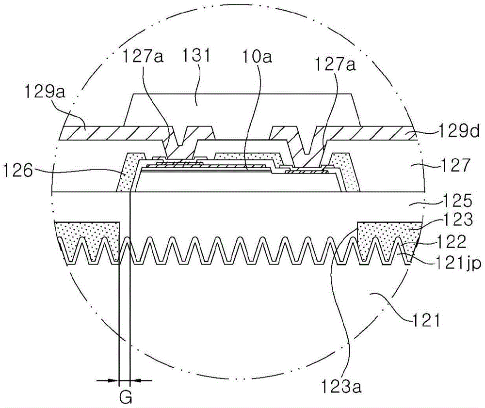
图3A是用于说明根据本公开的一实施例的单元像素100的示意性的平面图,图3B是沿图3A的剖切线B-B'剖切的示意性的剖面图,图3C是图3B的局部剖面图。3A is a schematic plan view illustrating a
参照图3A、图3B及图3C,单元像素100可以包括透明基板121、第一发光元件10a、第二发光元件10b及第三发光元件10c、表面层122、第一光阻断层123、粘合层125、第二光阻断层126、阶梯差调节层127、连接层129a、129b、129c、129d及绝缘物质层131。3A, 3B and 3C, the
单元像素100包括第一发光元件10a、第二发光元件10b及第三发光元件10c而提供一个像素。第一发光元件10a、第二发光元件10b及第三发光元件10c发出彼此不同的颜色的光,它们分别对应于子像素。The
透明基板121是PET、玻璃基板、石英、蓝宝石基板等的光透射性基板。透明基板121布置于显示装置(图1的显示装置10000)的光发出面,从发光元件10a、10b、10c发出的光通过透明基板121而向外部发出。透明基板121可以具有上表面及下表面。透明基板121可以在面对发光元件10a、10b、10c的面(即,上表面)包括凹凸图案121p。凹凸图案121p使从发光元件10a、10b、10c发出的光散射而增加指向角。并且,可以使从具有彼此不同的指向角特性的发光元件10a、10b、10c发出的光借由所述凹凸图案121p而以均匀的指向角发出。据此,可以防止根据视角而发生色差。The
凹凸图案121p可以是规则的,也可以是不规则的。凹凸图案121P例如可以具有3μm的间距(pitch)、2.8μm的直径及1.8μm的高度。凹凸图案121p可以是一般应用于图案化的蓝宝石基板的图案,但并不限于此。The concavo-
透明基板121还可以包括防反射涂层,或者可以包括防眩层或进行防眩处理。透明基板121例如可以具有50μm至300μm的厚度。The
由于透明基板121布置于光发出面,因此透明基板121不包括电路。然而,本公开并不限于此,也可以包括电路。Since the
另外,虽然示出了在一个透明基板121形成有一个单元像素100的情况,但也可以在一个透明基板121形成有多个单元像素100。In addition, although the case where one
表面层122覆盖透明基板121的凹凸图案121p。表面层122可以沿着凹凸图案121p的形状而形成。表面层122可以提高形成于其上的第一光阻断层123的粘合力。例如,表面层122可以利用氧化硅膜形成。也可以根据透明基板121的种类而省略表面层122。The
第一光阻断层123形成于透明基板121的上表面上。第一光阻断层123可以与表面层122接触。第一光阻断层123可以包括诸如炭黑之类的吸收光的吸收物质。光吸收物质防止在发光元件10a、10b、10c生成的光从透明基板121与发光元件10a、10b、10c之间的区域向侧表面侧泄漏,从而提高显示装置的对比度。The first
第一光阻断层123可以具有用于光行进路径的窗123a、123b、123c,以使在发光元件10a、10b、10c生成的光入射到透明基板121,为此,可以在透明基板121上以暴露透明基板121的方式进行图案化。窗123a、123b、123c的宽度可以小于发光元件的宽度,但并不限于此。例如,窗123a、123b、123c的宽度可以大于发光元件10a、10b、10c的宽度,据此,如图3C所示,可以在发光元件10a与第一光阻断层123之间形成有相当于宽度G的间隙。The first light-
粘合层125附着于透明基板121上。粘合层125可以覆盖第一光阻断层123。粘合层125可以附着于透明基板121的整个表面上,但并不限于此,也可以附着于局部区域以暴露透明基板121的边缘位置附近区域。粘合层125用于将发光元件10a、10b、10c附着于透明基板121。粘合层125可以填充形成在第一光阻断层123的窗123a、123b、123c。The
粘合层125可以形成为光透射性层,并使从发光元件10a、10b、10c发出的光透射。粘合层125可以利用有机粘合剂而形成。例如,粘合层125可以利用透明环氧树脂而形成。并且,为了使光扩散,粘合层125可以包括SiO2、TiO2、ZnO等的扩散物质(diffuser)。光扩散物质防止从光发出面观察到发光元件10a、10b、10c。The
另外,第一发光元件10a、第二发光元件10b及第三发光元件10c布置于透明基板121上。第一发光元件10a、第二发光元件10b及第三发光元件10c可以借由粘合层125而附着于透明基板121。第一发光元件10a、第二发光元件10b及第三发光元件10c可以与第一光阻断层123的窗123a、123b、123c对应而布置。In addition, the first
如图3B所示,第一发光元件10a、第二发光元件10b及第三发光元件10c可以布置于粘合层125的平坦的表面上。粘合层125可以布置于发光元件10a、10b、10c的下表面下方。在另一实施例中,粘合层125也可以局部地覆盖第一发光元件10a、第二发光元件10b及第三发光元件10c的侧表面。As shown in FIG. 3B , the first
第一发光元件10a、第二发光元件10b及第三发光元件10c例如可以是红色发光元件、绿色发光元件、蓝色发光元件。第一发光元件10a、第二发光元件10b及第三发光元件10c中的每一个的具体构成与参照图2A及图2B说明的内容相同,因此省略详细说明。The first
如图3A所示,第一发光元件10a、第二发光元件10b及第三发光元件10c可以排列成一列。尤其,在透明基板121为蓝宝石基板的情况下,蓝宝石基板可以根据切割方向包括由于晶面而干净的切割面(例如,m面)和不干净的切割面(例如,a面)。例如,在切割成四边形形状的情况下,两侧的两个切割面(例如,m面)可以沿着晶面而被干净地切割,与这些切割面垂直布置的其他两个切割面(例如,a面)可以被不干净地切割。在此情况下,蓝宝石基板121的干净的切割面可以与发光元件10a、10b、10c的整齐排列方向平行。例如,在图3A中,干净的切割面(例如,m面)可以布置于上下,另外两个切割面(例如,a面)可以布置于左右。As shown in FIG. 3A, the first
并且,第一发光元件10a、第二发光元件10b及第三发光元件10c可以分别排列为长轴方向彼此平行。第一发光元件10a、第二发光元件10b及第三发光元件10c的短轴方向可以与这些发光元件的整齐排列方向一致。In addition, the first light-emitting
第一发光元件10a、第二发光元件10b及第三发光元件10c可以是参照图2A及图2B说明的发光元件,然而并不限于此,可以使用水平型或倒装芯片结构的多样的发光元件。The first light-emitting
第二光阻断层126可以覆盖发光元件10a、10b、10c的侧表面。第二光阻断层126也可以覆盖发光元件10a、10b、10c的上表面。第二光阻断层126可以具有暴露发光元件10a、10b、10c的电极垫61、63的开口部。The second
如图3A所示,在发光元件10a、10b、10c上可以分别布置有第二光阻断层126,但是并不限于此,一个第二光阻断层126可以连续地覆盖发光元件10a、10b、10c。进而,第二光阻断层126的一部分可以覆盖粘合层125。在第一光阻断层123与第二光阻断层126之间可以布置有粘合层125,并且第一光阻断层123和第二光阻断层126可以借由粘合层125而隔开。As shown in FIG. 3A, second light-blocking
由于第二光阻断层126覆盖发光元件10a、10b、10c的侧表面,因此可以阻断从发光元件10a、10b、10c朝侧表面方向发出的光。据此,可以防止发光元件10a、10b、10c之间的光干涉。Since the second
进而,第二光阻断层126布置成覆盖在发光元件10a、10b、10c与第一光阻断层123之间形成的间隙。因此,可以防止不期望的光通过间隙发出。例如,从相邻的发光元件发出的光有可能在连接层129a、129b、129c、129d被反射而通过间隙发出。这样的光降低显示装置的颜色再现性,并对对比度产生不良影响。但是,由于第二光阻断层126布置成覆盖间隙G,因此可以防止不期望的光通过间隙而发出到外部,据此,可以提高颜色再现性并增加对比度。Furthermore, the second
第二光阻断层126可以利用与第一光阻断层123相同的物质形成,但并不限于此,也可以利用其他物质形成。第二光阻断层126可以吸收或反射光。The second
阶梯差调节层127覆盖第一发光元件10a、第二发光元件10b、第三发光元件10c以及第二光阻断层126。阶梯差调节层127具有暴露发光元件10a、10b、10c的第一电极垫61及第二电极垫63的开口部127a。阶梯差调节层127将形成连接层129a、129b、129c、129d的面的高度调节为恒定,从而有助于能够安全地形成连接层。例如,阶梯差调节层127可以利用光敏聚酰亚胺形成。The
阶梯差调节层127可以在第二光阻断层126的周围接触于粘合层125。阶梯差调节层127可以布置于被粘合层125的边缘位置包围的区域内,但并不限于此。例如,阶梯差调节层127也可以形成为局部地暴露粘合层125的边缘位置。The
阶梯差调节层127的侧表面可以相对于粘合层125的上表面以小于90度的角度倾斜。例如,阶梯差调节层127的侧表面可以相对于粘合层125的上表面具有约60度的倾斜角。Side surfaces of the
第一连接层129a、第二连接层129b、第三连接层129c及第四连接层129d形成于阶梯差调节层127上。连接层129a、129b、129c、129d可以通过阶梯差调节层127的开口部127a而连接于第一发光元件10a、第二发光元件10b及第三发光元件10c的第一电极垫61及第二电极垫63。The
在一实施例中,如图3A及图3B所示,第一连接层129a可以电连接于第一发光元件10a的第二导电型半导体层,第二连接层129b可以电连接于第二发光元件10b的第二导电型半导体层,第三连接层129c可以电连接于第三发光元件10c的第二导电型半导体层,第四连接层129d可以共同地电连接于第一发光元件10a的第一导电型半导体层、第二发光元件10b的第一导电型半导体层及第三发光元件10c的第一导电型半导体层。第一连接层129a、第二连接层129b、第三连接层129c及第四连接层129d可以一起形成于阶梯差调节层127上,且例如可以包括Au。In one embodiment, as shown in FIG. 3A and FIG. 3B , the
在另一实施例中,第一连接层129a可以电连接于第一发光元件10a的第一导电型半导体层,第二连接层129b可以电连接于第二发光元件10b的第一导电型半导体层,第三连接层129c可以电连接于第三发光元件10c的第一导电型半导体层,第四连接层129d可以共同地电连接于第一发光元件10a的第二导电型半导体层、第二发光元件10b的第二导电型半导体层及第三发光元件10c的第二导电型半导体层。第一连接层129a、第二连接层129b、第三连接层129c及第四连接层129d可以一起形成于阶梯差调节层127上。In another embodiment, the
绝缘物质层131可以形成为比阶梯差调节层127薄的厚度。绝缘物质层131和阶梯差调节层127的厚度之和可以为1um以上且50um以下,但并不限于此。另外,绝缘物质层131的侧表面可以相对于粘合层125的上表面具有小于90度的倾斜角,例如,可以具有约60度的倾斜角。The insulating
绝缘物质层131覆盖阶梯差调节层127的侧表面及连接层129a、129b、129c、129d。并且,绝缘物质层131可以覆盖粘合层125的一部分。绝缘物质层131具有暴露连接层129a、129b、129c、129d的开口部131a、131b、131c、131d,据此,可以定义单元像素100的垫区域。The insulating
在一实施例中,绝缘物质层131可以是半透明物质,并可以利用有机物质或无机物质形成。绝缘物质层131例如可以利用聚酰亚胺形成。在绝缘物质层131与阶梯差调节层127一起利用聚酰亚胺形成的情况下,连接层129a、129b、129c、129d除了垫区域之外,下部面、侧表面及上部面均可以被聚酰亚胺包围。In an embodiment, the insulating
另外,单元像素100可以利用焊料等的接合材料贴装于电路基板,接合材料可以接合暴露于绝缘物质层131的开口部131a、131b、131c、131d的连接层129a、129b、129c、129d与电路基板上的垫。In addition, the
根据本实施例,单元像素100不包括单独的凸块,连接层129a、129b、129c、129d用作接合垫。然而,本发明并不限于此,也可以形成覆盖绝缘物质层131的开口部131a、131b、131c、131d的接合垫。在一实施例中,可以形成为超出第一连接层129a、第二连接层129b、第三连接层129c及第四连接层129d的上部区域而局部地覆盖发光元件10a、10b、10c。According to the present embodiment, the
在本实施例中,对发光元件10a、10b、10c借由粘合层125而附着于透明基板121的情形进行了说明,但是也可以利用其他结合器(coupler)而代替粘合层125而使发光元件10a、10b、10c结合于透明基板121。例如,可以利用间隔件而使发光元件10a、10b、10c结合于透明基板121,因此,在发光元件10a、10b、10c与透明基板121之间的区域可以填充有气体或液体。借由这些气体或液体,可以形成使从发光元件10a、10b、10c发出的光透射的光学层。上述的粘合层125也是光学层的一示例。在此,光学层利用与发光元件10a、10b、10c不同的材料(例如,气体、液体或固体)形成,因此与发光元件10a、10b、10c内的半导体层的材料区分。In this embodiment, the case where the light-emitting
图4A是用于说明根据本公开的一实施例的像素模块1000的示意性的平面图,图4B是沿图4A的剖切线C-C'剖切的示意性的剖面图。FIG. 4A is a schematic plan view illustrating a
参照图4A及图4B,像素模块1000包括电路基板1001及排列在电路基板1001上的单元像素100。进而,像素模块1000还可以包括覆盖单元像素100的覆盖层1010。Referring to FIGS. 4A and 4B , the
电路基板1001可以具有用于电连接面板基板2100与发光元件10a、10b、10c的电路。电路基板1001内的电路可以形成为多层结构。电路基板1001还可以包括用于以无源矩阵驱动方式驱动发光元件10a、10b、10c的无源电路或用于以有源矩阵驱动方式驱动发光元件10a、10b、10c的有源电路。电路基板1001可以包括暴露于其表面的垫1003。The
单元像素100的具体构成与参照图3A及图3B说明的内容相同,因此为了避免重复,省略详细说明。单元像素100可以整齐排列在电路基板1001上。如图4A所示,单元像素100可以以2×2行列排列,但并不限于此,可以以2×3、3×3、4×4、5×5等多样的行列排列。The specific configuration of the
单元像素100借由接合材料1005而接合于电路基板1001。例如,接合材料1005将通过参照图3A及图3B说明的绝缘物质层131的开口部131a、131b、131c、131d而被暴露的连接层129a、129b、129c、129d接合于电路基板1001上的垫1003。接合材料1005例如可以是焊料,可以利用丝网印刷等技术将焊膏布置在垫1003上之后通过回流工艺而接合单元像素100和电路基板1001。The
根据本实施例,在连接层129a、129b、129c、129d与垫1003之间布置有单一结构的接合材料1005,接合材料1005可以将连接层129a、129b、129c、129d与垫1003直接连接。According to this embodiment, a
覆盖层1010覆盖多个单元像素100。覆盖层1010可以防止单元像素100之间的光干涉而提高显示装置的对比度。The
覆盖层1010例如可以利用干膜型阻焊剂(DFSR:dry-Film type solder resist)、光致成像阻焊剂(PSR:photoimageable solder resist)、黑色材料(BM:black material)或环氧模塑料(EMC)等而形成。覆盖层1010例如可以利用层压、旋涂、狭缝涂布、印刷等技术而形成。Covering
通过将图4A及图4B所示的像素模块1000贴装于图1的面板基板2100上,据此可以提供显示装置10000。电路基板1001具有连接于垫1003的底部垫。底部垫可以布置成与垫1003一一对应,但是可以通过共同连接而减少底部垫的数量。By mounting the
在本实施例中,单元像素100形成为像素模块1000,并将像素模块1000贴装于面板基板2100上,从而能够提供显示装置,据此,能够提高显示装置的工艺良率。但是,本发明并不限于此,也可以将单元像素100直接贴装于面板基板2100上。In this embodiment, the
图5是用于说明根据一实施例的单元像素200的示意性的剖面图。FIG. 5 is a schematic cross-sectional view illustrating a
参照图5,根据本实施例的单元像素200与参照图3A至图3C说明的单元像素100大致相似,不同之处在于,第二光阻断层126a和阶梯差调节层127a一起被图案化。Referring to FIG. 5 , the
即,在本实施例中,在连续涂覆第二光阻断层126a和阶梯差调节层127a之后,第二光阻断层126a和阶梯差调节层127a通过曝光及显影工序而一起被图案化,从而形成暴露发光元件10a、10b、10c的电极垫的开口部。That is, in the present embodiment, after the second light blocking layer 126a and the
据此,第二光阻断层126a的侧表面不被阶梯差调节层127a覆盖而暴露。阶梯差调节层127a借由第二光阻断层126a而与粘合层125隔开。并且,第二光阻断层126a也在暴露电极垫的开口部的侧壁暴露。Accordingly, the side surface of the second light blocking layer 126a is exposed without being covered by the
根据本实施例,可以一起对第二光阻断层126a和阶梯差调节层127a进行图案化,从而可以简化单元像素200的制造工艺。According to this embodiment, the second light blocking layer 126a and the step
图6是用于说明根据一实施例的单元像素300的示意性的剖面图。FIG. 6 is a schematic cross-sectional view illustrating a
参照图6,根据本实施例的单元像素300与参照图5说明的单元像素200大致相似,不同之处在于,省略了阶梯差调节层127a,而由第二光阻断层127b形成为一起执行光阻断功能与阶梯差调节层的功能。因此,第二光阻断层127b形成为比图5的第二光阻断层126a相对更厚,且阶梯差调节层127a被省略。第二光阻断层127b可以在发光元件10a、10b、10c的周围与粘合层125相接触,并且,可以与发光元件10a、10b、10c上部的绝缘物质层131相接触。Referring to FIG. 6, the
根据本实施例,由于不需要单独形成光阻断层和阶梯差调节层,因此可以进一步简化制造工艺。According to this embodiment, since the light blocking layer and the step difference adjustment layer do not need to be separately formed, the manufacturing process can be further simplified.
图7A至图7F是用于说明根据一实施例的单元像素100的制造方法的示意性的剖面图。7A to 7F are schematic cross-sectional views illustrating a method of manufacturing a
首先,参照图7A,在透明基板121的上表面形成凹凸图案121p。透明基板121是PET、玻璃基板、石英、蓝宝石基板等光透射性基板。在一实施例中,凹凸图案121p可以利用干式蚀刻技术或湿式蚀刻技术来蚀刻透明基板121的表面而形成。First, referring to FIG. 7A , a concavo-
表面层122可以形成于透明基板121上。表面层122可以沿着凹凸图案121p而形成。表面层122例如可以利用硅氧化膜形成。表面层122是为了对透明基板121的表面进行改性而形成的,也可以省略。The
参照图3A及图7B,在透明基板121上形成第一光阻断层123。第一光阻断层123可以利用吸收光的物质层(例如,包括吸收光的诸如炭黑之类的吸收物质的黑矩阵)形成。另外,第一光阻断层123可以利用光敏物质层形成,并可以通过曝光及显影来图案化。通过对第一光阻断层123进行图案化,可以形成窗123a、123b、123c。多个窗123a、123b、123c可以对应于发光元件10a、10b、10c而形成,这些窗123a、123b、123c可以彼此隔开。Referring to FIGS. 3A and 7B , a first
在本实施例中,示出了一个单元像素区域的剖面,但是透明基板121可以是具有例如4英寸、6英寸或8英寸等的直径的大面积基板。单元像素区域可以具有例如400nm×400nm以下、240nm×240nm以下的面积,因此,可以在透明基板121上以定义多个单元像素区域的方式形成第一光阻断层123。在各个单元像素区域形成窗123a、123b、123c。In this embodiment, a cross section of one unit pixel area is shown, but the
参照图3A及图7C,粘合层125可以形成在第一光阻断层123上。粘合层125可以覆盖第一光阻断层123,并且可以覆盖通过形成在光阻断层123的窗123a、123b、123c而暴露的表面层122或透明基板121。Referring to FIGS. 3A and 7C , an
粘合层125可以形成在透明基板121的整个表面上,但并不限于此,可以以暴露透明基板121的边缘位置附近区域的方式形成在局部区域。粘合层125用于将发光元件10a、10b、10c附着于透明基板121。粘合层125可以利用光透射性层形成,并使从发光元件10a、10b、10c发出的光透射。粘合层125可以利用粘合片或有机粘合剂而形成。例如,粘合层125可以利用透明环氧树脂形成。在一实施例中,为了使光扩散,粘合层125可以包括SiO2、TiO2、ZnO等的扩散物质(diffuser)。光扩散物质防止从光发出面观察到发光元件10a、10b、10c。如图7C所示,粘合层125可以覆盖第一光阻断层123的侧表面。The
接着,在粘合层125上布置发光元件10a、10b、10c。发光元件10a、10b、10c可以利用转印工艺而转印到粘合层125。在透明基板121上定义多个单元像素区域,各个发光元件10a、发光元件10b及发光元件10c可以通过单独的工艺而转印,且发光元件10a、10b、10c也可以一起转印。Next, the
发光元件10a、10b、10c可以分别对应于窗123a、123b、123c而布置。发光元件10a、10b、10c可以具有小于窗123a、123b、123c的尺寸,并且可以位于窗123a、123b、123c的上部区域内。在另一实施例中,发光元件10a、10b、10c也可以具有大于窗123a、123b、123c的面积。The
参照图3A及图7D,形成覆盖发光元件10a、10b、10c的第二光阻断层126。第二光阻断层126可以具有暴露各个发光元件10a、10b、10c的电极垫的开口部。第二光阻断层126可以通过形成覆盖粘合层125及发光元件10a、10b、10c的物质层并图案化该物质层来形成。第二光阻断层126尤其覆盖发光元件10a、10b、10c的侧表面,并且形成为覆盖发光元件10a、10b、10c与第一光阻断层123之间的间隙G(参照图3C)。Referring to FIG. 3A and FIG. 7D , a second light-
参照图3A及图7E,阶梯差调节层127形成为覆盖发光元件10a、10b、10c。阶梯差调节层127覆盖第二光阻断层126。阶梯差调节层127例如可以利用光敏聚酰亚胺形成,并可以利用曝光及显影技术来被图案化。Referring to FIG. 3A and FIG. 7E , the
阶梯差调节层127可以具有暴露发光元件10a、10b、10c的开口部127a。例如,阶梯差调节层127的开口部可以暴露发光元件10a、10b、10c的第一电极垫(图2B的第一电极垫61)及第二电极垫(图2B的第二电极垫63)。进而,阶梯差调节层127可以沿着透明基板121的边缘位置而被去除,从而暴露粘合层125。The level
参照图3A及图7F,在阶梯差调节层127上形成第一连接层129a、第二连接层129b、第三连接层129c及第四连接层129d。例如,第一连接层129a、第二连接层129b、第三连接层129c及第四连接层129d可以利用剥离技术而形成。Referring to FIG. 3A and FIG. 7F , a
第一连接层129a、第二连接层129b、第三连接层129c及第四连接层129d可以通过阶梯差调节层127的开口部127a而电连接于发光元件10a、10b、10c。例如,第一连接层129a、第二连接层129b及第三连接层129c可以分别电连接于发光元件10a、10b、10c的第一导电型半导体层,并且第四连接层129d可以共同地电连接于发光元件10a、10b、10c的第二导电型半导体层。The
接着,可以形成绝缘物质层131。绝缘物质层131覆盖第一连接层129a、第二连接层129b、第三连接层129c及第四连接层129d。如图3A所示,绝缘物质层131可以具有暴露第一连接层129a、第二连接层129b、第三连接层129c及第四连接层129d的开口部131a、131b、131c、131d,可以借由这些开口部131a、131b、131c、131d而定义垫区域。Next, an insulating
在本实施例中,以在形成第二光阻断层126之后形成阶梯差调节层127为例进行了说明,但也可以在连续涂覆第二光阻断层126和阶梯差调节层127之后一起被图案化来提供单元像素200,也可以省略第二光阻断层126并将阶梯差调节层127形成为光阻断物质层,从而形成单元像素300。In this embodiment, the
图8是用于说明根据又一实施例的单元像素的示意性的剖面图。FIG. 8 is a schematic cross-sectional view for explaining a unit pixel according to still another embodiment.
参照图8,根据本实施例的单元像素与参照图3A、图3B说明的单元像素100大致相似,不同之处在于第二光阻断层126连续地覆盖发光元件10a、10b、10c。即,第二光阻断层126在发光元件10a、10b、10c之间的区域中也覆盖粘合层125。另外,如图所示,第二光阻断层126的最外侧边缘可以布置为靠近发光元件10a、10b、10c,但并不限于此。在本实施例中,第二光阻断层126的最外侧边缘也可以在阶梯差调节层127的最外侧边缘与发光元件10a、10b、10c之间的任意区域。Referring to FIG. 8 , the unit pixel according to this embodiment is substantially similar to the
根据本实施例,可以防止通过发光元件10a、10b、10c之间的区域而产生光干涉,据此,可以使从发光元件10a、10b、10c发出的光更限定于对应的窗123a、123b、123c而发出。According to this embodiment, it is possible to prevent light interference from occurring in areas between the light-emitting
以上,对本公开的多样的实施例进行了说明,但本公开并不限于这些实施例。并且,在不脱离本公开的技术思想的情况下,针对一个实施例说明的事项或构成要素也可以应用于另一实施例。Various embodiments of the present disclosure have been described above, but the present disclosure is not limited to these embodiments. Furthermore, matters or constituent elements described for one embodiment may also be applied to another embodiment without departing from the technical idea of the present disclosure.
Claims (20)
Applications Claiming Priority (5)
| Application Number | Priority Date | Filing Date | Title |
|---|---|---|---|
| US202063092791P | 2020-10-16 | 2020-10-16 | |
| US63/092,791 | 2020-10-16 | ||
| US17/495,460 | 2021-10-06 | ||
| US17/495,460 US12080687B2 (en) | 2020-10-16 | 2021-10-06 | Unit pixel having light emitting device, method of fabricating the same, and displaying apparatus having the same |
| PCT/KR2021/014234 WO2022080890A1 (en) | 2020-10-16 | 2021-10-14 | Unit pixel having light-emitting element, method for manufacturing same, and display device having same |
Publications (1)
| Publication Number | Publication Date |
|---|---|
| CN116325193A true CN116325193A (en) | 2023-06-23 |
Family
ID=80404493
Family Applications (2)
| Application Number | Title | Priority Date | Filing Date |
|---|---|---|---|
| CN202122481350.2U Active CN215933632U (en) | 2020-10-16 | 2021-10-14 | Unit pixel and display device |
| CN202180069843.5A Pending CN116325193A (en) | 2020-10-16 | 2021-10-14 | Unit pixel with light-emitting element, manufacturing method of the unit pixel, and display device with the unit pixel |
Family Applications Before (1)
| Application Number | Title | Priority Date | Filing Date |
|---|---|---|---|
| CN202122481350.2U Active CN215933632U (en) | 2020-10-16 | 2021-10-14 | Unit pixel and display device |
Country Status (4)
| Country | Link |
|---|---|
| US (2) | US12080687B2 (en) |
| EP (1) | EP4231355A4 (en) |
| CN (2) | CN215933632U (en) |
| WO (1) | WO2022080890A1 (en) |
Cited By (1)
| Publication number | Priority date | Publication date | Assignee | Title |
|---|---|---|---|---|
| WO2025137943A1 (en) * | 2023-12-27 | 2025-07-03 | 湖北三安光电有限公司 | Unit pixel and display device |
Families Citing this family (1)
| Publication number | Priority date | Publication date | Assignee | Title |
|---|---|---|---|---|
| WO2025053310A1 (en) * | 2023-09-08 | 2025-03-13 | 엘지전자 주식회사 | Display device including semiconductor light-emitting elements |
Family Cites Families (14)
| Publication number | Priority date | Publication date | Assignee | Title |
|---|---|---|---|---|
| JP3387478B2 (en) * | 1999-06-30 | 2003-03-17 | セイコーエプソン株式会社 | Semiconductor device and manufacturing method thereof |
| US6730940B1 (en) | 2002-10-29 | 2004-05-04 | Lumileds Lighting U.S., Llc | Enhanced brightness light emitting device spot emitter |
| KR102256632B1 (en) * | 2015-01-21 | 2021-05-26 | 엘지이노텍 주식회사 | Light emitting device and e-beam evaporating apparatus manufacturing the same |
| WO2016161161A1 (en) * | 2015-03-31 | 2016-10-06 | Cree, Inc. | Light emitting diodes and methods with encapsulation |
| KR102323828B1 (en) | 2015-10-16 | 2021-11-10 | 서울바이오시스 주식회사 | Compact light emitting diode chip, light emitting device and electronic device including the same |
| US10340425B2 (en) | 2016-11-25 | 2019-07-02 | Seoul Viosys Co., Ltd. | Light emitting diode having light blocking layer |
| CN118263235A (en) | 2017-09-04 | 2024-06-28 | 首尔半导体株式会社 | Light-emitting device |
| KR102404905B1 (en) | 2017-11-10 | 2022-06-07 | 삼성전자주식회사 | Display appartus and manufacturing method for the same |
| US11271136B2 (en) * | 2018-11-07 | 2022-03-08 | Seoul Viosys Co., Ltd | Light emitting device |
| US11355686B2 (en) * | 2019-03-29 | 2022-06-07 | Seoul Semiconductor Co., Ltd. | Unit pixel having light emitting device, pixel module and displaying apparatus |
| KR102723703B1 (en) * | 2019-05-28 | 2024-10-31 | 삼성디스플레이 주식회사 | Display device and manufacturing method for display device |
| CN113169259A (en) * | 2019-11-04 | 2021-07-23 | 厦门三安光电有限公司 | Light-emitting diode and method of making the same |
| US20210399041A1 (en) * | 2020-06-18 | 2021-12-23 | Seoul Semiconductor Co., Ltd. | Light emitting module having a plurality of unit pixels, method of fabricating the same, and displaying apparatus having the same |
| US12027654B2 (en) * | 2020-09-11 | 2024-07-02 | Seoul Viosys Co., Ltd. | Unit pixel having light emitting device and displaying apparatus |
-
2021
- 2021-10-06 US US17/495,460 patent/US12080687B2/en active Active
- 2021-10-14 CN CN202122481350.2U patent/CN215933632U/en active Active
- 2021-10-14 EP EP21880537.2A patent/EP4231355A4/en active Pending
- 2021-10-14 CN CN202180069843.5A patent/CN116325193A/en active Pending
- 2021-10-14 WO PCT/KR2021/014234 patent/WO2022080890A1/en not_active Ceased
-
2024
- 2024-08-21 US US18/811,541 patent/US20240413135A1/en active Pending
Cited By (1)
| Publication number | Priority date | Publication date | Assignee | Title |
|---|---|---|---|---|
| WO2025137943A1 (en) * | 2023-12-27 | 2025-07-03 | 湖北三安光电有限公司 | Unit pixel and display device |
Also Published As
| Publication number | Publication date |
|---|---|
| US20240413135A1 (en) | 2024-12-12 |
| US20220123184A1 (en) | 2022-04-21 |
| EP4231355A1 (en) | 2023-08-23 |
| CN215933632U (en) | 2022-03-01 |
| EP4231355A4 (en) | 2024-11-20 |
| WO2022080890A1 (en) | 2022-04-21 |
| US12080687B2 (en) | 2024-09-03 |
Similar Documents
| Publication | Publication Date | Title |
|---|---|---|
| JP7775299B2 (en) | Highly efficient light emitting device, unit pixel having the same, and display device having the same | |
| US12364073B2 (en) | Unit pixel having light emitting device and displaying apparatus | |
| CN217641390U (en) | Pixel module and display device | |
| US20240413135A1 (en) | Unit pixel having light emitting device, method of fabricating the same, and displaying apparatus having the same | |
| US20250318332A1 (en) | Unit pixel having light emitting device and displaying apparatus | |
| US20250022856A1 (en) | Unit pixel and displaying apparatus including the unit pixel | |
| US20240313179A1 (en) | Unit pixel having light emitting device and displaying apparatus | |
| CN217336009U (en) | Circuit board, display device and pixel module | |
| CN214477447U (en) | Unit pixel and display device | |
| US20240243242A1 (en) | Unit pixel having light emitting device displaying apparatus | |
| CN215896385U (en) | Wafer for manufacturing unit pixel | |
| CN116918465A (en) | Circuit board with multi-layer solder resist and display device with the circuit board |
Legal Events
| Date | Code | Title | Description |
|---|---|---|---|
| PB01 | Publication | ||
| PB01 | Publication | ||
| SE01 | Entry into force of request for substantive examination | ||
| SE01 | Entry into force of request for substantive examination |