CN116248789A - Case and electronic device including case - Google Patents
Case and electronic device including case Download PDFInfo
- Publication number
- CN116248789A CN116248789A CN202310279936.1A CN202310279936A CN116248789A CN 116248789 A CN116248789 A CN 116248789A CN 202310279936 A CN202310279936 A CN 202310279936A CN 116248789 A CN116248789 A CN 116248789A
- Authority
- CN
- China
- Prior art keywords
- electronic device
- recess
- protrusion
- side member
- board
- Prior art date
- Legal status (The legal status is an assumption and is not a legal conclusion. Google has not performed a legal analysis and makes no representation as to the accuracy of the status listed.)
- Granted
Links
Images






Classifications
-
- H—ELECTRICITY
- H04—ELECTRIC COMMUNICATION TECHNIQUE
- H04M—TELEPHONIC COMMUNICATION
- H04M1/00—Substation equipment, e.g. for use by subscribers
- H04M1/02—Constructional features of telephone sets
- H04M1/18—Telephone sets specially adapted for use in ships, mines, or other places exposed to adverse environment
-
- H—ELECTRICITY
- H05—ELECTRIC TECHNIQUES NOT OTHERWISE PROVIDED FOR
- H05K—PRINTED CIRCUITS; CASINGS OR CONSTRUCTIONAL DETAILS OF ELECTRIC APPARATUS; MANUFACTURE OF ASSEMBLAGES OF ELECTRICAL COMPONENTS
- H05K5/00—Casings, cabinets or drawers for electric apparatus
- H05K5/0017—Casings, cabinets or drawers for electric apparatus with operator interface units
-
- H—ELECTRICITY
- H05—ELECTRIC TECHNIQUES NOT OTHERWISE PROVIDED FOR
- H05K—PRINTED CIRCUITS; CASINGS OR CONSTRUCTIONAL DETAILS OF ELECTRIC APPARATUS; MANUFACTURE OF ASSEMBLAGES OF ELECTRICAL COMPONENTS
- H05K5/00—Casings, cabinets or drawers for electric apparatus
- H05K5/0086—Casings, cabinets or drawers for electric apparatus portable, e.g. battery operated apparatus
-
- G—PHYSICS
- G06—COMPUTING OR CALCULATING; COUNTING
- G06F—ELECTRIC DIGITAL DATA PROCESSING
- G06F1/00—Details not covered by groups G06F3/00 - G06F13/00 and G06F21/00
- G06F1/16—Constructional details or arrangements
- G06F1/1613—Constructional details or arrangements for portable computers
- G06F1/1626—Constructional details or arrangements for portable computers with a single-body enclosure integrating a flat display, e.g. Personal Digital Assistants [PDAs]
-
- G—PHYSICS
- G06—COMPUTING OR CALCULATING; COUNTING
- G06F—ELECTRIC DIGITAL DATA PROCESSING
- G06F1/00—Details not covered by groups G06F3/00 - G06F13/00 and G06F21/00
- G06F1/16—Constructional details or arrangements
- G06F1/1613—Constructional details or arrangements for portable computers
- G06F1/1633—Constructional details or arrangements of portable computers not specific to the type of enclosures covered by groups G06F1/1615 - G06F1/1626
- G06F1/1637—Details related to the display arrangement, including those related to the mounting of the display in the housing
-
- G—PHYSICS
- G06—COMPUTING OR CALCULATING; COUNTING
- G06F—ELECTRIC DIGITAL DATA PROCESSING
- G06F1/00—Details not covered by groups G06F3/00 - G06F13/00 and G06F21/00
- G06F1/16—Constructional details or arrangements
- G06F1/1613—Constructional details or arrangements for portable computers
- G06F1/1633—Constructional details or arrangements of portable computers not specific to the type of enclosures covered by groups G06F1/1615 - G06F1/1626
- G06F1/1656—Details related to functional adaptations of the enclosure, e.g. to provide protection against EMI, shock, water, or to host detachable peripherals like a mouse or removable expansions units like PCMCIA cards, or to provide access to internal components for maintenance or to removable storage supports like CDs or DVDs, or to mechanically mount accessories
-
- H—ELECTRICITY
- H04—ELECTRIC COMMUNICATION TECHNIQUE
- H04M—TELEPHONIC COMMUNICATION
- H04M1/00—Substation equipment, e.g. for use by subscribers
- H04M1/02—Constructional features of telephone sets
- H04M1/0202—Portable telephone sets, e.g. cordless phones, mobile phones or bar type handsets
- H04M1/0249—Details of the mechanical connection between the housing parts or relating to the method of assembly
-
- H—ELECTRICITY
- H05—ELECTRIC TECHNIQUES NOT OTHERWISE PROVIDED FOR
- H05K—PRINTED CIRCUITS; CASINGS OR CONSTRUCTIONAL DETAILS OF ELECTRIC APPARATUS; MANUFACTURE OF ASSEMBLAGES OF ELECTRICAL COMPONENTS
- H05K5/00—Casings, cabinets or drawers for electric apparatus
- H05K5/02—Details
- H05K5/0217—Mechanical details of casings
Landscapes
- Engineering & Computer Science (AREA)
- Computer Hardware Design (AREA)
- Theoretical Computer Science (AREA)
- General Engineering & Computer Science (AREA)
- Microelectronics & Electronic Packaging (AREA)
- Signal Processing (AREA)
- Human Computer Interaction (AREA)
- Physics & Mathematics (AREA)
- General Physics & Mathematics (AREA)
- Casings For Electric Apparatus (AREA)
Abstract
提供了一种电子装置的壳体和电子装置。包括至少一个板的电子装置的壳体包括:第一表面,其联接到至少一个板的板的至少一部分并面向板的后表面;以及构件,其包括第二表面,第二表面大体上垂直于第一表面并面向板的侧表面,并且其中第一表面包括从第一表面朝向板突出预定高度的突起、从第一表面形成预定深度的第一凹部、以及从第一表面形成比第一凹部更深的第二凹部。
Provided are a casing of an electronic device and the electronic device. A housing of an electronic device including at least one board includes: a first surface coupled to at least a portion of the board of the at least one board and facing a rear surface of the board; and a member including a second surface substantially perpendicular to the The first surface faces the side surface of the board, and wherein the first surface includes a protrusion protruding from the first surface toward the board by a predetermined height, a first recess formed from the first surface to a predetermined depth, and a first recess formed from the first surface Deeper second recess.
Description
技术领域technical field
本公开涉及电子装置的壳体以及包括该壳体的电子装置。The present disclosure relates to a case of an electronic device and an electronic device including the case.
背景技术Background technique
电子装置(例如,移动电话)可以输出存储的信息作为声音或图像。随着集成度的提高和高速大容量无线通信的普及,单个移动通信终端具有多种功能。例如,诸如游戏的娱乐功能、诸如音乐/视频文件的再现的多媒体功能、用于移动银行等的通信和安全功能、调度功能、电子钱包功能等以及通信功能已经被集成在单个电子装置中。由于电子装置可以执行各种功能,因此可以在电子装置的内部包括多个不同的电子部件。Electronic devices (eg, mobile phones) can output stored information as sound or images. With the improvement of integration and the popularization of high-speed and large-capacity wireless communication, a single mobile communication terminal has multiple functions. For example, entertainment functions such as games, multimedia functions such as reproduction of music/video files, communication and security functions for mobile banking, etc., scheduling functions, electronic wallet functions, etc., and communication functions have been integrated in a single electronic device. Since an electronic device can perform various functions, a plurality of different electronic components can be included inside the electronic device.
此外,为了保护电子元件免受外部冲击,限定电子装置的外观的壳体需要高耐久性。当制造电子装置的壳体时,至少一个板和构件彼此联接以完成电子装置的外观。各种联接方法可用于连接至少一个板和构件。In addition, in order to protect electronic components from external shocks, high durability is required for the case defining the appearance of the electronic device. When manufacturing a case of an electronic device, at least one board and a member are coupled to each other to complete the appearance of the electronic device. Various joining methods are available for joining at least one panel and member.
上述信息仅作为背景信息来呈现,以帮助理解本公开。关于上述中的任何一个是否可以作为关于本公开的现有技术适用,没有做出任何确定,并且没有做出断言。The above information is presented as background information only to facilitate an understanding of the present disclosure. No determination has been made, and no assertion is made, as to whether any of the above might be applicable as prior art with respect to the present disclosure.
发明内容Contents of the invention
技术问题technical problem
包括在电子装置的壳体中的各种部件可以通过使用粘合材料彼此联接。例如,当板和支撑所述板的构件彼此联接时,可以使用将粘合材料施加到所述构件的一侧(例如,上表面)并将所述板组装到施加有所述粘合材料的所述构件上的方法。Various components included in the case of the electronic device may be coupled to each other by using an adhesive material. For example, when a board and a member supporting the board are coupled to each other, applying an adhesive material to one side (for example, an upper surface) of the member and assembling the board to a member to which the adhesive material is applied may be used. method on the component.
在使用液态粘合材料的情况下,待粘合的物体可能由于挤压而变形,并且在一些情况下,粘合材料的一部分可能偏离物体的粘合区域并溢出到外部。当制造电子装置的壳体时,溢出到壳体外部的粘合材料可能成为降低电子装置的外观的吸引人方面的原因。In the case of using a liquid adhesive material, objects to be bonded may be deformed due to extrusion, and in some cases, a part of the adhesive material may deviate from the bonding area of the object and overflow to the outside. When the case of the electronic device is manufactured, the adhesive material overflowing to the outside of the case may be a cause of reducing the attractive aspect of the appearance of the electronic device.
近年来,在包括显示器的电子装置中,由于边框(或黑矩阵(BM)区域)的小型化,用于为包括显示器的板进行安置接合的区域逐渐减小。同时,为了满足电子装置所需的粘合力,必须使用预定量或更多的粘合材料。根据一些情况,因为需要使用预定量或更多的粘合材料,同时减小电子装置的粘接面积,所以可能难以防止粘合材料泄漏到电子装置的外部。In recent years, in an electronic device including a display, due to miniaturization of a bezel (or black matrix (BM) area), an area for mounting bonding for a panel including a display has been gradually reduced. Meanwhile, in order to satisfy the adhesive force required for electronic devices, a predetermined amount or more of an adhesive material must be used. According to some cases, since it is necessary to use a predetermined amount or more of the adhesive material while reducing the adhesive area of the electronic device, it may be difficult to prevent the adhesive material from leaking to the outside of the electronic device.
本公开的方面是解决至少上述问题和/或缺点,并提供至少下述优点。因此,本公开的一个方面是提供这样一种电子装置的壳体以及包括该壳体的电子装置,该壳体固定施加到联接源上的适当量的粘合材料并以保持粘接力并且防止粘合材料溢出到电子装置壳体的外部。Aspects of the present disclosure are to address at least the above-mentioned problems and/or disadvantages and to provide at least the advantages described below. Accordingly, an aspect of the present disclosure is to provide a casing of an electronic device that secures an appropriate amount of adhesive material applied to a coupling source to maintain adhesive force and prevent Adhesive material overflows to the exterior of the electronics housing.
另外的方面将部分地在随后的描述中阐述,并且部分地将从描述中显而易见,或者可以通过所呈现的实施例的实践来获知。Additional aspects will be set forth in part in the description which follows and, in part, will be obvious from the description, or may be learned by practice of the presented embodiments.
问题的解决方案problem solution
根据本公开的一个方面,提供了一种电子装置。电子装置包括第一板、面对第一板的相反方向的第二板、以及侧部构件,侧部构件附接到第二板或与第二板一体地形成、围绕包括第一板和第二板之间的至少一个电子元件的空间并且联接到第一板,其中侧部构件包括面对第一板的后表面的第一表面以及基本上垂直于第一表面并且面对第一板的侧表面的第二表面,并且其中第一表面包括:突起,其从第一表面向上突出,使得第一板基本上安置在第一表面上;第一凹部,其设置在突起和第二表面之间,并且沿着侧部构件的长度方向从第一表面凹进第一深度;以及第二凹部,其沿着侧部构件的长度方向从第一表面凹进第二深度。According to an aspect of the present disclosure, an electronic device is provided. The electronic device includes a first board, a second board facing an opposite direction of the first board, and a side member attached to or integrally formed with the second board, surrounding the first board and the second board. Space for at least one electronic component between the two boards and coupled to the first board, wherein the side member includes a first surface facing the rear surface of the first board and a first surface substantially perpendicular to the first surface and facing the first board The second surface of the side surface, and wherein the first surface includes: a protrusion protruding upward from the first surface so that the first plate is basically placed on the first surface; a first recess disposed between the protrusion and the second surface and a second recess recessed from the first surface to a second depth along the length of the side member.
根据本公开的另一方面,提供了包括至少一个板的电子装置壳体。电子装置的壳体包括连接到至少一个板的板的后表面的构件,其中构件包括面对板的后表面的第一表面和布置成基本上垂直于第一表面并面对板的侧表面的第二表面,并且其中第一表面包括:从第一表面向上突出使得板基本上安置在第一表面上的突起、从第一表面沿着构件的长度方向凹进第一深度的第一凹部、以及从第一表面沿着构件的长度方向凹进第二深度的第二凹部。According to another aspect of the present disclosure, an electronic device case including at least one board is provided. The housing of the electronic device includes a member connected to a rear surface of a board of at least one board, wherein the member includes a first surface facing the rear surface of the board and a side surface arranged substantially perpendicular to the first surface and facing the side surface of the board. the second surface, and wherein the first surface comprises: a protrusion protruding upwardly from the first surface such that the plate is substantially seated on the first surface, a first recess recessed from the first surface to a first depth along the length of the member, and a second recess recessed to a second depth from the first surface along the length direction of the member.
根据本公开的另一方面,提供了一种包括至少一个板的电子装置壳体。电子装置的壳体包括:第一表面,其联接到至少一个板的板的至少一部分并面向板的后表面;以及构件,其包括大体上垂直于第一表面并面向板的侧表面的第二表面,并且其中第一表面包括从第一表面朝向板突出预定高度的突起、从第一表面凹进预定深度的第一凹部、以及从第一表面凹部得比第一凹部更深的第二凹部。According to another aspect of the present disclosure, there is provided an electronic device case including at least one board. The housing of the electronic device includes: a first surface coupled to at least a portion of a board of at least one board and facing a rear surface of the board; and a member including a second surface substantially perpendicular to the first surface and facing a side surface of the board. surface, and wherein the first surface includes a protrusion protruding from the first surface toward the plate by a predetermined height, a first recess recessed from the first surface to a predetermined depth, and a second recess recessed from the first surface deeper than the first recess.
发明的有益效果Beneficial Effects of the Invention
根据本公开的各种实施例的电子装置和电子装置的壳体可以防止施加到壳体的粘合材料溢出,同时不减少粘合材料的量。The electronic device and the case of the electronic device according to various embodiments of the present disclosure may prevent the adhesive material applied to the case from overflowing while not reducing the amount of the adhesive material.
根据本公开的各种实施例的电子装置和电子装置的壳体可以通过结构方法防止粘合材料溢出。因此,本公开可防止电子装置的外观的吸引人的方面在制造电子装置壳体的过程中劣化。The electronic device and the case of the electronic device according to various embodiments of the present disclosure may prevent adhesive material from overflowing through a structural method. Therefore, the present disclosure can prevent the attractive aspects of the appearance of the electronic device from being degraded in the process of manufacturing the case of the electronic device.
通过下面结合附图的详细描述,本公开的其它方面、优点和显著特征对于本领域技术人员将变得显而易见,详细描述公开了本公开的各种实施例。Other aspects, advantages, and salient features of the present disclosure will become apparent to those skilled in the art from the following detailed description, which discloses various embodiments of the present disclosure, when taken in conjunction with the accompanying drawings.
附图说明Description of drawings
从以下结合附图的描述中,本公开的某些实施例的上述和其它方面、特征和优点将变得更加明显,其中:The above and other aspects, features and advantages of certain embodiments of the present disclosure will become more apparent from the following description taken in conjunction with the accompanying drawings, in which:
图1是根据本公开的实施例的网络环境中的电子装置的框图;1 is a block diagram of an electronic device in a network environment according to an embodiment of the present disclosure;
图2A是根据本公开的实施例的电子装置的前部立体图;2A is a front perspective view of an electronic device according to an embodiment of the present disclosure;
图2B是根据本公开的实施例的电子装置的后部立体图;2B is a rear perspective view of an electronic device according to an embodiment of the present disclosure;
图3是示出根据本公开的实施例的电子装置的分解立体图;3 is an exploded perspective view illustrating an electronic device according to an embodiment of the present disclosure;
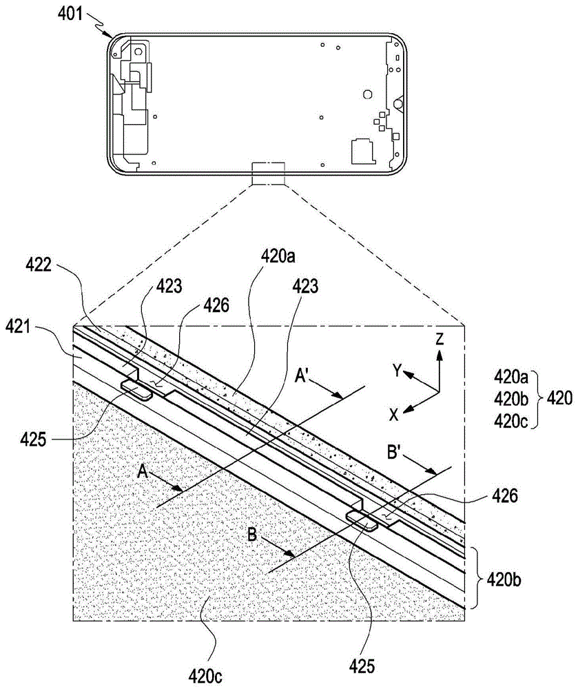
图4是示出根据本公开的实施例的电子装置壳体及其一部分的放大立体图的视图;4 is a view showing an enlarged perspective view of an electronic device housing and a portion thereof according to an embodiment of the present disclosure;
图5是示出根据本公开的实施例的将粘合材料施加到侧部构件的状态的视图;5 is a view showing a state of applying an adhesive material to a side member according to an embodiment of the present disclosure;
图6是示出根据本公开的实施例的在第一板和侧部构件之间插入粘合材料的状态的视图;6 is a view illustrating a state in which an adhesive material is inserted between a first plate and a side member according to an embodiment of the present disclosure;
图7是示出根据本公开的实施例的在第一板和侧部构件之间插入粘合材料的状态的视图;7 is a view illustrating a state in which an adhesive material is inserted between a first plate and a side member according to an embodiment of the present disclosure;
图8是示出根据本公开的实施例的壳体的截面的视图;FIG. 8 is a view showing a section of a case according to an embodiment of the present disclosure;
图9是示出根据本公开的实施例的从顶部观察根据图8的实施例的侧部构件的视图;FIG. 9 is a view showing a side member according to the embodiment of FIG. 8 viewed from the top according to an embodiment of the present disclosure;
图10是示出根据本公开的实施例的电子装置壳体的截面的视图;10 is a view illustrating a cross section of an electronic device case according to an embodiment of the present disclosure;
图11A、图11B和图11C是示出根据本公开的各种实施例的突起的布置形式的视图;以及11A, 11B, and 11C are views illustrating arrangement forms of protrusions according to various embodiments of the present disclosure; and
图12A和图12B是示出根据本公开的各种实施例的电子装置壳体的截面的视图。12A and 12B are views illustrating a cross-section of an electronic device case according to various embodiments of the present disclosure.
在所有附图中,应当注意,相同的附图标记用于描述相同或相似的元件、特征和结构。Throughout the drawings, it should be noted that like reference numbers are used to depict the same or similar elements, features, and structures.
具体实施方式Detailed ways
提供以下参考附图的描述以帮助全面理解如由权利要求书及其等效物界定的本公开的各种实施例。它包括各种具体细节以帮助理解,但是这些仅被认为是示例性的。因此,本领域的普通技术人员将认识到,在不脱离本公开的范围和精神的情况下,可以对这里描述的各种实施例进行各种改变和修改。此外,为了清楚和简洁起见,可以省略对众所周知的功能和结构的描述。The following description with reference to the accompanying drawings is provided to assist in a comprehensive understanding of various embodiments of the present disclosure as defined by the claims and their equivalents. It includes various specific details to aid in that understanding, but these are to be regarded as exemplary only. Accordingly, those of ordinary skill in the art will recognize that various changes and modifications of the various embodiments described herein can be made without departing from the scope and spirit of the disclosure. Also, descriptions of well-known functions and constructions may be omitted for clarity and conciseness.
在以下描述和权利要求书中使用的术语和词不限于书目含义,而是仅由发明人使用以使得能够清楚和一致地理解本公开。因此,本领域的技术人员应当清楚,提供本公开的各种实施例的以下描述仅仅是为了说明的目的,而不是为了限制由所附权利要求及其等同物限定的本公开。The terms and words used in the following description and claims are not limited to the bibliographical meanings, but, are merely used by the inventor to enable a clear and consistent understanding of the present disclosure. Accordingly, it should be apparent to those skilled in the art that the following description of various embodiments of the present disclosure is provided for illustration purpose only and not for the purpose of limiting the disclosure as defined by the appended claims and their equivalents.
应当理解,单数形式“一个”、“一种”和“该”包括复数指示物,除非上下文另有明确规定。因此,例如,提及“部件表面”包括提及一个或多个这样的表面。It should be understood that the singular forms "a", "an" and "the" include plural referents unless the context clearly dictates otherwise. Thus, for example, reference to "a component surface" includes reference to one or more of such surfaces.
图1是示出根据各种实施例的网络环境100中的电子装置101的框图。参照图1,网络环境100中的电子装置101可经由第一网络198(例如,短距离无线通信网络)与电子装置102进行通信,或者经由第二网络199(例如,长距离无线通信网络)与电子装置104或服务器108进行通信。根据实施例,电子装置101可经由服务器108与电子装置104进行通信。根据实施例,电子装置101可包括处理器120、存储器130、输入装置150、声音输出装置155、显示装置160、音频模块170、传感器模块176、接口177、触觉模块179、相机模块180、电力管理模块188、电池189、通信模块190、用户识别模块(SIM)196或天线模块197。在一些实施例中,可从电子装置101中省略部件中的至少一个(例如,显示装置160或相机模块180),或者可将一个或更多其它部件添加到电子装置101中。在一些实施例中,可将部件中的一些部件实现为单个集成电路。例如,可将传感器模块176(例如,指纹传感器、虹膜传感器、或照度传感器)实现为嵌入在显示装置160(例如,显示器)中。FIG. 1 is a block diagram illustrating an electronic device 101 in a
处理器120可运行例如软件(例如,程序140)来控制电子装置101的与处理器120连接的至少一个其它部件(例如,硬件部件或软件部件),并可执行各种数据处理或计算。根据实施例,作为数据处理或计算的至少部分,处理器120可将从另一部件(例如,传感器模块176或通信模块190)接收到的命令或数据加载到易失性存储器132中,对存储在易失性存储器132中的命令或数据进行处理,并将结果数据存储在非易失性存储器134中。根据实施例,处理器120可包括主处理器121(例如,中央处理器(CPU)或应用处理器(AP))以及与主处理器121在操作上独立的或者相结合的辅助处理器123(例如,图形处理单元(GPU)、图像信号处理器(ISP)、传感器中枢处理器或通信处理器(CP))。另外地或者可选择地,辅助处理器123可被适配为比主处理器121耗电更少,或者被适配为具体用于指定的功能。可将辅助处理器123实现为与主处理器121分离,或者实现为主处理器121的部分。The
在主处理器121处于未激活(例如,睡眠)状态时,辅助处理器123可控制与电子装置101(而非主处理器121)的部件之中的至少一个部件(例如,显示装置160、传感器模块176或通信模块190)相关的功能或状态中的至少一些,或者在主处理器121处于激活状态(例如,运行应用)时,辅助处理器123可与主处理器121一起来控制与电子装置101的部件之中的至少一个部件(例如,显示装置160、传感器模块176或通信模块190)相关的功能或状态中的至少一些。根据实施例,可将辅助处理器123(例如,图像信号处理器或通信处理器)实现为在功能上与辅助处理器123相关的另一部件(例如,相机模块180或通信模块190)的部分。When the
存储器130可存储由电子装置101的至少一个部件(例如,处理器120或传感器模块176)使用的各种数据。各种数据可包括例如软件(例如,程序140)以及针对与其相关的命令的输入数据或输出数据。存储器130可包括易失性存储器132或非易失性存储器134。The
可将程序140作为软件存储在存储器130中,并且程序140可包括例如操作系统(OS)142、中间件144或应用146。The
输入装置150可从电子装置101的外部(例如,用户)接收将由电子装置101的其它部件(例如,处理器120)使用的命令或数据。输入装置150可包括例如麦克风、鼠标、键盘或数字笔(例如,手写笔)。The
声音输出装置155可将声音信号输出到电子装置101的外部。声音输出装置155可包括例如扬声器或接收器。扬声器可用于诸如播放多媒体或播放唱片的通用目的,接收器可用于呼入呼叫。根据实施例,可将接收器实现为与扬声器分离,或实现为扬声器的部分。The
显示装置160可向电子装置101的外部(例如,用户)视觉地提供信息。显示装置160可包括例如显示器、全息装置或投影仪以及用于控制显示器、全息装置和投影仪中的相应一个的控制电路。根据实施例,显示装置160可包括被适配为检测触摸的触摸电路或被适配为测量由触摸引起的力的强度的传感器电路(例如,压力传感器)。The
音频模块170可将声音转换为电信号,反之亦可。根据实施例,音频模块170可经由输入装置150获得声音,或者经由声音输出装置155或与电子装置101直接(例如,有线地)连接或无线连接的外部电子装置(例如,电子装置102)的耳机输出声音。The
传感器模块176可检测电子装置101的操作状态(例如,功率或温度)或电子装置101外部的环境状态(例如,用户的状态),然后产生与检测到的状态相应的电信号或数据值。根据实施例,传感器模块176可包括例如手势传感器、陀螺仪传感器、大气压力传感器、磁性传感器、加速度传感器、握持传感器、接近传感器、颜色传感器、红外(IR)传感器、生物特征传感器、温度传感器、湿度传感器或照度传感器。The
接口177可支持将用来使电子装置101与外部电子装置(例如,电子装置102)直接(例如,有线地)或无线连接的一个或更多特定协议。根据实施例,接口177可包括例如高清晰度多媒体接口(HDMI)、通用串行总线(USB)接口、安全数字(SD)卡接口或音频接口。The
连接端178可包括连接器,其中,电子装置101可经由连接器与外部电子装置(例如,电子装置102)物理连接。根据实施例,连接端178可包括例如HDMI连接器、USB连接器、SD卡连接器或音频连接器(例如,耳机连接器)。The
触觉模块179可将电信号转换为可被用户经由他的触觉或动觉识别的机械刺激(例如,振动或运动)或电刺激。根据实施例,触觉模块179可包括例如电机、压电元件或电刺激器。The
相机模块180可捕获静止图像或运动图像。根据实施例,相机模块180可包括一个或更多镜头、图像传感器、图像信号处理器或闪光灯。The
电力管理模块188可管理对电子装置101的供电。根据实施例,可将电力管理模块188实现为例如电力管理集成电路(PMIC)的至少部分。The
电池189可对电子装置101的至少一个部件供电。根据实施例,电池189可包括例如不可再充电的原电池、可再充电的蓄电池、或燃料电池。The
通信模块190可支持在电子装置101与外部电子装置(例如,电子装置102、电子装置104或服务器108)之间建立直接(例如,有线)通信信道或无线通信信道,并经由建立的通信信道执行通信。通信模块190可包括能够与处理器120(例如,应用处理器(AP))独立操作的一个或更多通信处理器,并支持直接(例如,有线)通信或无线通信。根据实施例,通信模块190可包括无线通信模块192(例如,蜂窝通信模块、短距离无线通信模块或全球导航卫星系统(GNSS)通信模块)或有线通信模块194(例如,局域网(LAN)通信模块或电力线通信(PLC)模块)。这些通信模块中的相应一个可经由第一网络198(例如,短距离通信网络,诸如蓝牙、无线保真(Wi-Fi)直连或红外数据协会(IrDA))或第二网络199(例如,长距离通信网络,诸如蜂窝网络、互联网、或计算机网络(例如,LAN或广域网(WAN)))与外部电子装置进行通信。可将这些各种类型的通信模块实现为单个部件(例如,单个芯片),或可将这些各种类型的通信模块实现为彼此分离的多个部件(例如,多个芯片)。无线通信模块192可使用存储在用户识别模块196中的用户信息(例如,国际移动用户识别码(IMSI))识别并验证通信网络(诸如第一网络198或第二网络199)中的电子装置101。The
天线模块197可将信号或电力发送到电子装置101的外部(例如,外部电子装置)或者从电子装置101的外部(例如,外部电子装置)接收信号或电力。根据实施例,天线模块197可包括天线,天线包括辐射元件,辐射元件由形成在基底(例如,PCB)中或形成在基底上的导电材料或导电图案构成。根据实施例,天线模块197可包括多个天线。在这种情况下,可由例如通信模块190(例如,无线通信模块192)从多个天线中选择适合于在通信网络(诸如第一网络198或第二网络199)中使用的通信方案的至少一个天线。随后可经由所选择的至少一个天线在通信模块190和外部电子装置之间发送或接收信号或电力。根据实施例,除了辐射元件之外的另外的部件(例如,射频集成电路(RFIC))可附加地形成为天线模块197的一部分。The
上述部件中的至少一些可经由外设间通信方案(例如,总线、通用输入输出(GPIO)、串行外设接口(SPI)或移动工业处理器接口(MIPI))相互连接并在它们之间通信地传送信号(例如,命令或数据)。At least some of the aforementioned components may be connected to each other and between them via an inter-peripheral communication scheme (e.g., bus, general-purpose input-output (GPIO), serial peripheral interface (SPI), or mobile industry processor interface (MIPI)). Signals (eg, commands or data) are communicated.
根据实施例,可经由与第二网络199连接的服务器108在电子装置101和外部电子装置104之间发送或接收命令或数据。电子装置102和电子装置104中的每一个可以是与电子装置101相同类型的装置,或者是与电子装置101不同类型的装置。根据实施例,将在电子装置101运行的全部操作或一些操作可在外部电子装置102、外部电子装置104或服务器108中的一个或更多运行。例如,如果电子装置101应该自动执行功能或服务或者应该响应于来自用户或另一装置的请求执行功能或服务,则电子装置101可请求一个或更多外部电子装置执行功能或服务中的至少部分,而不是运行功能或服务,或者电子装置101除了运行功能或服务以外,还可请求一个或更多外部电子装置执行功能或服务中的至少部分。接收到请求的一个或更多外部电子装置可执行功能或服务中的所请求的至少部分,或者执行与请求相关的另外功能或另外服务,并将执行的结果传送到电子装置101。电子装置101可在对结果进行进一步处理的情况下或者在不对结果进行进一步处理的情况下将结果提供作为对请求的至少部分答复。为此,可使用例如云计算技术、分布式计算技术或客户机-服务器计算技术。According to an embodiment, commands or data may be transmitted or received between the electronic device 101 and the external
图2A是根据本公开的实施例的电子装置的前部立体图。图2B是根据本公开的实施例的电子装置的后部立体图。FIG. 2A is a front perspective view of an electronic device according to an embodiment of the present disclosure. 2B is a rear perspective view of an electronic device according to an embodiment of the present disclosure.
参照图2A和图2B,根据实施例的电子装置200(例如,图1的101)可以包括壳体210,该壳体210包括第一表面(或前表面)210A、第二表面(或后表面)210B和侧表面210C,该侧表面210C围绕第一表面210A和第二表面210B之间的空间。在另一个实施例(未示出)中,壳体可以指限定图2A的第一表面210A、第二表面210B和侧表面210C中的一些的结构。根据实施例,第一表面210A可以由前板202(例如,包括各种涂层的玻璃板或聚合物板)限定,该前板的至少一部分基本上是透明的。第二表面210B可以由基本上不透明的后板211限定。后板211例如可以由涂覆的或着色的玻璃、陶瓷、聚合物、金属(例如铝、不锈钢(STS)或镁)或其至少两种的组合形成。侧表面210C可以联接到前板202和后板211,并且可以由包括金属和/或聚合物的侧边框结构(或“侧部构件”)218限定。在一些实施例中,后板211和侧边框结构218可以一体形成,并且可以包括相同的材料(例如,诸如铝的金属材料)。Referring to FIGS. 2A and 2B , an electronic device 200 (eg, 101 of FIG. 1 ) according to an embodiment may include a
在所示实施例中,前板202可以包括两个第一区域210D,它们在前板202的长边的相对端处从第一表面210A朝向后板211偏转并无缝地延伸。在所示实施例(参见图2A)中,后板211可以包括两个第二区域210E,它们在后板211的长边的相对端处从第二表面210B朝向前板202偏转并无缝地延伸。在一些实施例中,前板202(或后板211)可以仅包括第一区域210D(或第二区域210E)中的一个。在其它实施例中,可以不包括第一区域210D或第二区域210E中的一些。在实施例中,当从电子装置200的一侧观看时,侧边框结构218可以在既不包括第一区域210D也不包括第二区域210E的侧表面上具有第一厚度(宽度),并且可以在包括第一区域210D或第二区域210E的侧表面上具有小于第一厚度的第二厚度。In the illustrated embodiment, the
根据实施例,电子装置200可以包括显示器201、音频模块203、207、214、传感器模块204、216和219、相机模块205、212和213、键输入装置217、发光元件206以及连接器孔208和209中的至少一个。在一些实施例中,可以从电子装置200中省略元件中的至少一个(例如,键输入装置217或发光元件206),或者可以在电子装置200中另外包括另一个部件。According to an embodiment, the
例如,显示器201可以通过前板202的相应部分露出。在一些实施例中,显示器201的至少一部分可以通过限定第一表面210A和侧表面210C的第一区域210D的前板202暴露。在一些实施例中,显示器201的拐角可以具有与前板202的相邻外部形状基本上相同的形状。在其它实施例(未示出)中,为了扩展显示器201暴露的区域,显示器201的外边缘和前板202的外边缘之间的间隔可以基本上相同。For example, the
在其它实施例(未示出)中,显示器201的屏幕显示区域的一部分可以具有凹部或开口,并且可以包括与凹部或开口对准的音频模块214、传感器模块204、相机模块205和发光元件206中的至少一个。在其它实施例(未示出)中,音频模块214、传感器模块204、相机模块205、指纹传感器216和发光元件206中的至少一个可以包括在显示器201的屏幕显示区域的后表面上。在其它实施例(未示出)中,显示器201可以联接到触摸检测电路、可以测量触摸的强度(压力)的压力传感器和/或检测磁场类型的触笔的数字化仪,或者设置成邻近它们。在一些实施例中,传感器模块204和219的至少一部分和/或键输入装置217的至少一部分可以设置在第一区域210D和/或第二区域210E中。In other embodiments (not shown), a portion of the screen display area of the
音频模块203、207、214可以包括麦克风孔203和扬声器孔207和214。用于获取外部声音的麦克风可以设置在麦克风孔203中,并且在一些实施例中,可以设置多个麦克风以检测声音的方向。扬声器孔207和214可以包括外部扬声器孔207和通信接收器孔214。在一些实施例中,扬声器孔207和214以及麦克风孔203可以通过一个孔来实现,或者可以包括扬声器而不使用扬声器孔207和214(例如,压电扬声器)。The
传感器模块204、216和219可以生成对应于电子装置200内部的操作状态或外部的环境状态的电信号或数据值。传感器模块204、216和219例如可以包括设置在壳体210的第一表面210A上的第一传感器模块204(例如,接近传感器)和第二传感器模块(未示出)(例如,指纹传感器)和/或设置在壳体210的第二表面210B上的第三传感器模块219(例如,心率监视器(HRM)传感器)和/或第四传感器模块216(例如,指纹传感器)。指纹传感器不仅可以设置在第一表面210A(例如,显示器201)上,而且可以设置在壳体210的第二表面210B上。电子装置200还可以包括传感器模块(未示出),例如手势传感器、陀螺仪传感器、大气压力传感器、磁传感器、加速度传感器、握持传感器、颜色传感器、红外(IR)传感器、生物测定传感器、温度传感器、湿度传感器或照明传感器中的至少一个。The
相机模块205、212和213可以包括设置在电子装置200的第一表面210A上的第一相机装置205以及设置在第二表面210B上的第二相机装置212和/或闪光灯213。相机装置205和212可以包括一个或多个镜头、图像传感器和/或图像信号处理器。例如,闪光灯213可以包括发光二极管或氙灯。在一些实施例中,可以在电子装置200的一个表面上设置两个或更多镜头(红外线相机和广角/远距镜头)和图像传感器。The
键输入装置217可以设置在壳体210的侧表面210C上。在另一个实施例中,电子装置200可以不包括上述键输入装置217中的一些或全部,并且未被包括的键输入装置217可以在显示器201上以不同的形式实现,例如软键。在一些实施例中,键输入装置可以包括设置在壳体210的第二表面210B上的传感器模块216。A
例如,发光器件206可以设置在壳体210的第一表面210A上。例如,发光元件206可以以光的形式在电子装置200上提供状态信息。在其它实施例中,例如,发光元件206可以提供与相机模块205的操作相互配合的光源。例如,发光元件206可以包括发光二极管(LED)、IR LED和氙灯。For example, the
连接器孔208和209可以包括第一连接器孔208和/或第二连接器孔(例如耳机插孔)209,第一连接器孔208可以容纳用于向外部电子装置发送电力和/或数据和从外部电子装置接收电力和/或数据的连接器(例如USB连接器),第二连接器孔209可以容纳用于向外部电子装置发送音频信号和从外部电子装置接收音频信号的连接器。The
图3是示出根据本公开的实施例的电子装置的分解立体图。FIG. 3 is an exploded perspective view illustrating an electronic device according to an embodiment of the present disclosure.
参照图3,电子装置300(例如,图2A的电子装置200)可包括侧边框结构310(例如,图2A的侧边框结构218)、第一支撑构件311(例如,支架)、前板320(例如,图2A的前板202)、显示器330(例如,图2A的显示器201)、印刷电路板340、电池350、第二支撑构件360(例如,后壳)、天线370和后板380(例如,图2B的后板211)。在一些实施例中,可以从电子装置300中省略元件中的至少一个(例如,第一支撑构件311或第二支撑构件360),或者可以在电子装置300中另外包括另一个部件。电子装置300的至少一个部件可以与图2A和图2B的可穿戴电子装置200的至少一个部件相同或相似,并且将省略其重复描述。Referring to FIG. 3 , an electronic device 300 (eg, the
第一支撑构件311可设置在电子装置300的内部以连接到侧边框结构310或与侧边框结构310一体形成。例如,第一支撑构件311可以由金属材料和/或非金属材料(例如,聚合物)形成。显示器330可以联接到第一支撑构件311的一个表面,并且印刷电路板340可以联接到第一支撑构件311的相对表面。处理器、存储器和/或接口可以安装在印刷电路板340上。例如,处理器可以包括中央处理单元、应用处理器、图形处理单元、图像信号处理器、传感器集线器进程或通信处理器中的一个或多个。The first supporting
例如,存储器可以包括易失性和/或非易失性存储器。For example, memory may include volatile and/or non-volatile memory.
例如,接口可以包括高清晰度多媒体接口(HDMI)、通用串行总线(USB)、SD卡接口和/或音频接口。例如,接口可以将电子装置300电或物理地连接到外部电子装置,并且可以包括USB连接器、SD卡/存储卡(MMC)连接器和音频连接器。For example, the interface may include a High-Definition Multimedia Interface (HDMI), a Universal Serial Bus (USB), an SD card interface, and/or an audio interface. For example, the interface may electrically or physically connect the
电池350是用于向电子装置300的至少一个部件提供电力的装置,并且例如可以包括不能被再充电的一次电池、可以被再充电的二次电池或燃料电池。例如,电池350的至少一部分可以设置在与印刷电路板340基本相同的平面上。电池350可以整体地设置在电子装置300的内部,并且可以设置成可从电子装置300拆卸。The
天线370可以设置在后板380和电池350之间。天线370例如可以包括近场通信(NFC)天线、无线充电天线和/或磁安全传输(MST)天线。例如,天线370可以执行与外部装置的短距离通信,或者可以无线地发送和接收用于充电的电力。在另一个实施例中,天线结构可以由侧边框结构310和/或第一支撑构件311中的一个或其组合形成。The
图4是示出根据本公开的实施例的电子装置壳体401及其一部分的放大立体图的视图。FIG. 4 is a view showing an enlarged perspective view of an
根据本公开的各种实施例的电子装置400(例如,图2A的电子装置200)可以包括各种形式的壳体401。The electronic device 400 (eg, the
如图2A至图3所描述,壳体401可包括前板(下文称为“第一板(或板)”、后板(下文称为“第二板(或板)”)和侧边框结构(下文称为“侧部构件或构件”)。2A to 3, the
根据本公开的各种实施例的壳体401可以由单一材料形成,或者可以由至少两种或更多种材料的组合形成。此外,根据各种实施例,壳体401可以由单个部件形成,但是可以由至少两个或更多部件形成。The
参照图4,图4示出了作为壳体401的示例的侧部构件420。根据图4所示的实施例的侧部构件420可以通过连接两种或多种材料形成。例如,侧部构件420可以是由陶瓷、聚合物、金属或至少两种材料的组合形成的部件。Referring to FIG. 4 , FIG. 4 shows a
根据各种实施例,侧部构件420可包括构成壳体外观的第一构件420a以及位于第一构件420a内部的第二构件420b和/或第三构件420c。根据实施例,第一构件420a可以是电子装置壳体中的插入注射模制部件。第二构件420b可以是与第一构件420a或第三构件420c基本相同的部分,或者可以是与第一构件420a或第三构件420c分开形成的部分。根据实施例,第一构件420a、第二构件420b和第三构件420c可以是基本上相同的部分。According to various embodiments, the
根据各种实施例的各种形式可用作本公开的侧部构件420。实施例的多样性可以类似地应用于图4中未示出的壳体401的其它构造(例如,第一板和第二板)。尽管为了便于描述,在下面的描述中将举例说明侧部构件420由单一材料形成,但是应当注意,本公开不限于此。Various forms according to various embodiments may be used as the
根据各种实施例,电子装置壳体401的侧部构件(或构件)420可以包括用于联接到壳体401的另一部分(安置在其上)的联接表面。例如,再次参考图4,侧部构件420可以包括第一表面421和第二表面422。第一表面421可以是壳体401的另一种结构,例如,面对板的一个表面(例如,后表面)的表面(例如,第一板),而第二表面422可以是壳体的另一种结构,例如,面对板的相对表面(例如,侧表面)的表面(例如,第一板)。According to various embodiments, the side member (or member) 420 of the
根据各种实施例,第一表面421和第二表面422可以沿着侧部构件420的长度方向(例如,平行于y轴的方向)延伸得较长。According to various embodiments, the
根据各种实施例,从侧部构件420的第一表面421沿着侧部构件420的长度方向(例如,平行于y轴的方向)形成第一深度的第一凹部423可以设置在侧部构件420的第一表面421上。According to various embodiments, the
如在图4所示的实施例中,根据本公开的各种实施例,类似于沿着侧部构件420的长度方向(例如,平行于y轴的方向)延伸得较长的第一表面421,第一凹部423也沿着侧部构件420的长度方向(例如,平行于y轴的方向)延伸得较长。根据实施例,第一凹部423可以具有在第一表面421上部分断裂的形状,但是根据另一个实施例,可以在第一表面421上一体地延伸得较长。As in the embodiment shown in FIG. 4 , according to various embodiments of the present disclosure, similar to the
根据各种实施例,从第一表面421向上突出的突起425可以设置在侧部构件420的第一表面421上。突起425可以是板(例如,第一板)基本上位于其上的部分。According to various embodiments, a
根据本公开的各种实施例,从侧部构件420的第一表面421沿着侧部构件420的长度方向(例如,平行于y轴的方向)形成第二深度的第二凹部426可以设置在侧部构件420的第一表面421上。According to various embodiments of the present disclosure, the
根据各种实施例,第二凹部426的至少一部分可以与第一凹部423重叠。根据实施例,如图4所示,在第二凹部426的整个部分与第一凹部423重叠的状态下,第二凹部426可以具有从第一凹部423形成得更深的形状。According to various embodiments, at least a portion of the
根据各种实施例,可以在第一表面421上设置多个突起425。这里,多个突起425可以设置成彼此隔开预定距离。According to various embodiments, a plurality of
根据各种实施例,多个第二凹部426也可以设置在第一表面421上。这里,多个第二凹部426可以设置成彼此隔开预定距离。根据各种实施例,第二凹部426可以设置成与突起425的位置相对应。According to various embodiments, a plurality of
图5是示出根据本公开的实施例将粘合材料430施加到侧部构件420的状态的视图。参照图5,图5可以是在图4的实施例中突起425和第二凹部426所设置的部分的局部放大视图。FIG. 5 is a view illustrating a state in which an
图5可以示出在将粘合材料430施加到第一表面421和突起425上之后粘合材料430流入第一凹部423和第二凹部426之前的状态。FIG. 5 may illustrate a state before the
根据各种实施例,丙烯(acryl)粘合剂或硅粘合剂可用作本公开的粘合材料430。然而,本公开不限于此,而是可以不同地确定粘合材料430的种类和组成。According to various embodiments, acryl adhesive or silicon adhesive may be used as the
根据实施例,粘合材料430可以沿着侧部构件420的长度方向(例如,平行于图4的y轴的方向)例如从侧部构件420的上端到下端施加得较长。According to an embodiment, the
粘合材料430可以施加到第一表面421和突起425中的至少一个上。施加到第一表面421和突起425中的至少一个上的粘合材料430可以流入第一凹部423和第二凹部426中并固化。An
将参考从图6开始的实施例详细描述第一凹部423的附加描述。将参考从图7开始的实施例详细描述突起425和第二凹部426的附加描述。Additional description of the first
图6是示出根据本公开的实施例的粘合材料430插入在第一板410和侧部构件420之间的状态的视图。图6示出了沿方向A-A'截取的图4的实施例中的壳体的结构的截面图。FIG. 6 is a view illustrating a state where an
参照图6,根据本公开的各种实施例的电子装置400(例如,图2A的电子装置200)可以包括在其内部限定空间的壳体401(例如,图2A的壳体210)以及设置在空间中的至少一个或多个部件(例如,部件440)。Referring to FIG. 6 , an electronic device 400 (for example, the
壳体401可包括第一板410、第二板和侧部构件420。The
根据各种实施例,第一板410可以是其至少一部分基本上透明的前板(例如,图2A的前板202)(例如,包括各种涂层的玻璃板、聚合物板或陶瓷板)或其基本上不透明的后板(例如,图2B的后板211)(例如,通过涂覆的或着色的玻璃、陶瓷、聚合物、金属或材料中的至少两种的组合设置的板)。According to various embodiments,
根据各种实施例,第二板可以是面向与第一板410相反的方向(或远离第一板410的方向)的板。根据实施例,在第一板410是电子装置的前板(例如,图2A的前板202)的情况下,第二板可以是电子装置的后板(例如,图2B的后板211)。根据另一个实施例,第一板410可以是电子装置400的后板(例如,图2B的后板211),第二板可以是电子装置400的前板(例如,图2A的前板202)。According to various embodiments, the second board may be a board facing in a direction opposite to the first board 410 (or in a direction away from the first board 410). According to an embodiment, in case the
根据各种实施例,侧部构件420可对应于联接到第一板410和/或第二板的结构。根据实施例,侧部构件420可以作为第二板的单独结构连接。根据另一个实施例,侧部构件420可以是作为与第二板的整体构造从第二板的周边延伸的部分。According to various embodiments, the
根据各种实施例,侧部构件420可包括面对第一板410的后表面411的第一表面421和面对第一板410的侧表面的第二表面422。第一表面421可以面对第一板410的后表面411的至少一部分,并且第二表面422可以面对第一板410的侧表面412的至少一部分。根据实施例,第一表面421可以面向与壳体(例如,图2A的壳体210)的第一表面(例如,图2A的第一表面210A)相同的方向。According to various embodiments, the
根据实施例,可以在第一板410和侧部构件420之间插入粘合材料430。图6可以示出在将粘合材料430施加到第一表面421和第一突起425上之后在粘合材料430流入第一凹部423之前的状态。根据实施例,图6可以示出其中挤压粘合材料430的状态。根据实施例,粘合材料430可以在连接第一板410和侧部构件420的过程中被挤压,并且可以在被挤压的粘合材料430的至少一部分被引入到第一板410和侧部构件420之间的间隙(例如,间隙g和第一凹部423)中的状态下被固化。According to an embodiment, an
第一凹部423可以设置在侧部构件420的第一表面421上。第一凹部423可以是从第一表面421形成第一深度的部分,并且可以设置在第一表面421连接到第二表面422的部分。在粘合材料430插在第一板410和侧部构件420之间的状态下,当第一板410和侧部构件420彼此联接时被挤压的粘合材料430可以被引入到第一凹部423中。引入到第一凹部423中的粘合材料430可以被固化。当通过固化的粘合材料430对电子装置施加物理冲击或者电子装置掉落时,第一板410和侧部构件420可以保持牢固的外观而不被分离。The
一起参照图5和图6,根据各种实施例,第一凹部423沿着将粘合材料430施加到侧部构件420的第一表面421上的部分设置,并且当第一板410位于侧部构件420的第一表面421上时,由于被挤压的粘合材料430的一部分流入第一凹部423,可以防止粘合材料430溢出到电子装置400的外部。Referring to FIGS. 5 and 6 together, according to various embodiments, the
根据实施例,当第一凹部423设置在侧部构件420的第一表面421上时,可视状态防止结构424可设置在第一凹部423和第二表面422之间。下面将参考图12对可视状态防止结构424进行详细描述。According to an embodiment, when the
图7是示出根据本公开的实施例的粘合材料430插入在第一板410和侧部构件420之间的状态的视图。图7示出了沿方向B-B'截取的图4的实施例中的壳体的结构的截面。FIG. 7 is a view illustrating a state where an
图7可以示出在将粘合材料430施加到第一表面421和突起425上之后粘合材料430流入第一凹部423和第二凹部426中的状态。根据实施例,图7可以示出与图6的实施例类似地挤压粘合材料430的状态。FIG. 7 may illustrate a state where the
参照图7,根据各种实施例,侧部构件420可以包括第一表面421和第二表面422,并且第一凹部423可以设置在第一表面421上。与图6的实施例不同,突起425和第二凹部426可以设置在本公开的侧部构件420的第一表面421上。Referring to FIG. 7 , according to various embodiments, the
突起425可以是第一板410的后表面411基本上位于其上的部分,并且可以在具有预定长度和预定宽度的同时从第一表面621突出预定高度。根据一些实施例,因为粘合材料430由液态材料形成,所以待粘接的物体之间的距离根据物体被挤压的程度可以不是恒定的。如果侧部构件420包括突起425,即使第一板410和侧部构件420之间的距离变短,第一板410和侧部构件420之间的距离也可以保持恒定。The
根据实施例,突起425可以与第一表面421一体地形成,或者可以由与第一表面421的材料分开的材料形成,并且可以是通过单独的工艺附接到第一表面421的部件。According to an embodiment, the
根据实施例,突起425可以定位成比第一凹部423更远离第二表面422。According to an embodiment, the
如参考图5所描述的,粘合材料430可以被施加到第一表面421和突起425的上部二者上,并且随着第一板和侧部构件420变得更靠近,施加到突起425的上部分的粘合材料430可以比施加到第一表面421的粘合材料430更早地被挤压,并且可以比施加到第一表面421的粘合材料430被挤压得更远。As described with reference to FIG. 5,
第二凹部426可以是沿着侧部构件420的长度方向延伸较长的部分。与第一凹部423沿着侧部构件420的长度方向延伸得较长的特征类似,第二凹部426也可以沿着侧部构件420的长度方向延伸得较长。The second
根据各种实施例,第二凹部426的至少一部分可以与第一表面421上的第一凹部423重叠。第二凹部426与第一凹部423重叠的特征可意味着第二凹部426在侧部构件的高度方向(例如,平行于图4的z轴的方向)上形成在距第一凹部423较深的位置。例如,第一凹部423可以从第一表面421形成第一深度(例如,图8的P1,其将在下面描述),而第二凹部426可以从第一表面421形成第二深度(例如,图8的P1+P2,其将在下面描述)。According to various embodiments, at least a portion of the
在图4、图5和图7中,第二凹部426的整个部分与第一凹部423重叠,并且可以形成在远离第一凹部423的位置。然而,尽管在附图中未示出,但是应当注意,不是整个部分而是仅第二凹部426的一部分可以与第一凹部423重叠。In FIGS. 4 , 5 and 7 , the entire portion of the
参照图5和图7,第二凹部426可以设置成与突起425的位置相对应地平行于突起425。因为第二凹部426设置在与突起425的位置对应的位置处,所以施加到突起425上的粘合材料430可以被引入到第二凹部426中。因为第二凹部426平行于突起425设置,所以在挤压粘合材料430的过程中,施加到突起425上的粘合材料430可以均匀地被引入到由第二凹部426限定的空间中。根据各种实施例,第二凹部426可包括至少一个倾斜表面427。至少一个倾斜表面427可以引导施加到第一表面421和突起425上的粘合材料430,使得在挤压粘合材料430的过程中,粘合材料430均匀地被引入到由第二凹部426限定的空间中。Referring to FIGS. 5 and 7 , the
一起参照图6和图7,例如,当在第一表面421上仅存在第一凹部423时(例如,图6的实施例),施加到第一表面421上的粘合材料430可以流入凹部423并固化。此外,如果进一步提供突起425,则与突起425的体积相对应的粘合材料430可能溢出到间隙G之间,并且与不存在突起425的实施例(例如,图6的实施例)相比,当粘合材料430溢出到电子装置的外部时,可能妨碍电子装置外观的吸引人的方面。Referring to FIGS. 6 and 7 together, for example, when there is only the
根据本公开的各种实施例,由于通过在邻近突起425的位置附加地设置第二凹部426(例如,图7的实施例),使得位于突起425上的粘合材料430流入第二凹部426中,因此可以根据粘合区域防止粘合材料430溢出到电子装置的外部,而不限制施加到粘合有粘合材料430的区域(或空间)的粘合材料430的量。According to various embodiments of the present disclosure, since the
图8是示出根据本公开的实施例的壳体401的截面的视图。FIG. 8 is a view showing a cross section of a
图9是示出根据本公开的实施例的从顶部观察根据图8的实施例的侧部构件420的视图。FIG. 9 is a view illustrating the
参照图8和图9,将讨论本公开的突起425和第二凹部426的尺寸。Referring to FIGS. 8 and 9 , dimensions of the
根据各种实施例,由第二凹部426限定的空间的深度P2大于突起425的高度H。由第二凹部426限定的空间的深度可以是通过从深度P1+P2减去由第一凹部423限定的空间的深度P1而获得的深度,通过该深度P1+P2从第一表面形成第二凹部426。According to various embodiments, the depth P2 of the space defined by the
根据各种实施例,当从侧部构件420的顶部观察时,第二凹部426的长度L1可以大于突起425的长度L2。因为第二凹部426的长度L1比突起425的长度L2长,所以当存在于突起425和/或围绕它们的第一表面421上的粘合材料流入第二凹部426并固化时,可以防止在第二凹部426的倾斜表面427周围产生的气穴。例如,当突起425的长度L2约为0.5mm至0.8mm时,第二凹部的长度L1约为0.8mm至1.2mm。According to various embodiments, the length L1 of the
根据各种实施例,当从侧部构件420的顶部观察时,第二凹部426的端部可以比突起425的端部长第一距离d1,并且第二凹部426的相对端可以比突起425的相对端长第二距离d2。因为第二凹部426的端部至少位于从穿过突起425和第二凹部426的假想线(例如,图10的A-A',将在下面描述)的中心开始的突起425的端部的外侧,所以可以引导被挤压的粘合材料流入第二凹部426,同时防止其沿另一方向流动。根据实施例,第一距离d1和第二距离d2可以是相同的长度。例如,第一距离d1和第二距离d2可以是0.2mm。According to various embodiments, when viewed from the top of the
根据各种实施例,第二凹部426的宽度W1可以大于突起425的宽度W2。According to various embodiments, the width W1 of the
总之,根据第二凹部426的宽度W1和长度L1而定的第二凹部426的体积以及由第二凹部426限定的空间的深度P2可以大于根据突起425的宽度W2、长度L2和高度而定的突起425的体积。In short, the volume of the
根据实施例,由第二凹部426限定的空间的体积可以被设计成与突起425的体积成比例。According to an embodiment, the volume of the space defined by the
根据本公开的各种实施例,由于在利用设置突起425的优点的同时额外设置了至少大于突起425的第二凹部426,突起425可以防止粘合材料430溢出到电子装置的外部。According to various embodiments of the present disclosure, since the
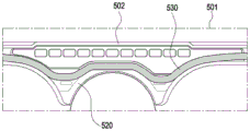
图10是示出根据本公开的实施例的电子装置壳体501的截面的视图。FIG. 10 is a view showing a cross section of an
根据各种实施例,将粘合材料530施加到侧部构件520上的部分可以不必是第一表面。According to various embodiments, the portion where the
如上所述,通过图4的实施例,根据各种实施例,侧部构件520不仅可以是单一材料或单一部件,而且可以是其中联接了不同材料或不同部件的构造。As mentioned above, with the embodiment of FIG. 4 , according to various embodiments, the
根据本公开的各种实施例,粘合材料530不仅可以施加到单个材料或单个部件的表面上,而且还可以施加到不同材料或不同部件的表面上。根据实施例,粘合材料530也可以被施加到不同材料或不同部件之间的边界。According to various embodiments of the present disclosure, the
参照图10,粘合材料530也可以施加到设置在侧部构件520上的装饰构件502上。粘合材料530可以与装饰构件502的至少一部分重叠。这样,与上述实施例不同,粘合材料530的位置可以是不同的。如图10所示,粘合材料530可以不必平行于侧部构件520的长度方向设置,而是粘合材料530的至少一部分可以具有弯曲的形状。Referring to FIG. 10 , an
根据各种实施例,突起(例如,图4的突起425)、第一凹部(例如,图4的第一凹部423)和第二凹部(例如,图4的凹部426)可以沿着其中施加粘合材料530的区域设置。According to various embodiments, a protrusion (eg,
如上所述,对应于侧面构件520上的各种应用位置和形式的粘合材料530,突起(例如,图4的突起425)、第一凹部(例如,图4的第一凹部723)和第二凹部(例如,图8的凹部426)的位置和形式可以被不同地指定。此外,上面参考图4至图9描述的各个实施例可以类似地应用于图10。As mentioned above, corresponding to the various application locations and forms of
图11A至图11C是示出根据本公开的各种实施例的突起625的布置形式的视图。11A to 11C are views illustrating an arrangement form of
根据各种实施例,突起625的位置和形式可以根据实施例而不同。在图11A至图11C中,示出了具有第一板610(例如,图7的第一板410)和侧部构件620(例如,图7的侧部构件420)的电子装置壳体601。According to various embodiments, the position and form of the
图11A可以示出其中突起625位于第一表面(例如,图7的第一表面421)的周边的实施例,图11B可以示出其中突起625位于第一表面(例如,图7的第一表面421)的相对周边处的实施例,图11C可以示出其中突起625位于第一表面(例如,图7的第一表面421)的中心的实施例。尽管未单独示出,但与附图中所示的不同,可以将各种实施例应用于突起625的截面形状。FIG. 11A can show an embodiment in which the
参照图11A至图11C,突起625可以靠近第一表面(例如,图7的第一表面421)上的电子元件(例如,图7的电子元件440)设置(例如,图11A),并且可以设置成靠近第二表面(例如,图7的第二表面422)。否则,突起625可以设置在第一表面(例如,图7的第一表面421)的刚好中央处。Referring to FIGS. 11A to 11C, the
突起625的位置可以根据第一凹部623和第二凹部626的体积和形成的形状而不同地确定。The position of the
图12A和图12B是示出根据本公开的各种实施例的电子装置壳体701的截面的视图。12A and 12B are views illustrating a cross-section of an
在图12A和图12B中,突起725可以设置在第一表面(例如,图7的第一表面421)上,并且可以设置在第二表面(例如,图7的第二表面422)附近。In FIGS. 12A and 12B , the
参照图12A,图12A可以示出具有第一板710(例如,图7的第一板410)和侧部构件720(例如,图7的侧部构件420)的电子装置壳体701,侧部构件720在不存在第二凹部的状态下设置有可视状态防止结构724。Referring to FIG. 12A, FIG. 12A may illustrate an
参照图12B,图12B可以示出当存在第二凹部726时从其去除可视状态防止结构的电子装置壳体701。Referring to FIG. 12B , FIG. 12B may illustrate the
例如,可视状态防止结构724可以是用于防止被引入到第一凹部723中并不均匀地粘接到第一凹部723上的粘合材料从外部可见的结构。在第一板710和侧部构件720彼此联接之后,可以在第一板710的一侧(例如,图7的侧412)和侧部构件720的一侧(例如,图7的侧422)之间形成间隙(例如,图7的间隙g),并且可以提供可视状态防止结构724以防止不均匀地引入到第一凹部的内部中的粘合材料从外部可见。根据实施例,可视状态防止结构724可以通过使可视状态防止结构724的面积大于间隙g的面积来防止被不均匀地引入到第一凹部内部的粘合材料可视。For example, the visible
根据实施例,通过附加地设置第二凹部726,可以减小被引入到凹部中的粘合材料被不均匀地固化的可能性。因此,添加第二凹部726的实施例可以具有去除可视状态防止结构724或减小可视状态防止结构724的尺寸的优点。According to an embodiment, by additionally providing the
根据本文公开的各种实施例的电子装置可以是各种类型的装置之一。电子装置可包括例如便携式通信装置(例如,智能电话)、计算机装置、便携式多媒体装置、便携式医疗装置、相机、可穿戴装置或家用电器。根据实施例,电子装置不限于以上的那些电子装置。An electronic device according to various embodiments disclosed herein may be one of various types of devices. Electronic devices may include, for example, portable communication devices (eg, smartphones), computer devices, portable multimedia devices, portable medical devices, cameras, wearable devices, or home appliances. According to an embodiment, the electronic device is not limited to those above.
应该理解的是,本公开的各种实施例以及其中使用的术语并不意图将在此阐述的技术特征限制于具体实施例,而是包括针对相应实施例的各种改变、等同形式或替换形式。对于附图的描述,相似的参考标号可用来指代相似或相关的元件。将理解的是,与术语相应的单数形式的名词可包括一个或更多事物,除非相关上下文另有明确指示。如这里所使用的,诸如“A或B”、“A和B中的至少一个”、“A或B中的至少一个”、“A、B或C”、“A、B和C中的至少一个”以及“A、B或C中的至少一个”的短语中的每一个短语可包括在与多个短语中的相应一个短语中一起列举出的项的所有可能组合。如这里所使用的,诸如“第1”和“第2”或者“第一”和“第二”的术语可用于将相应部件与另一部件进行简单区分,并且不在其它方面(例如,重要性或顺序)限制部件。将理解的是,在使用了术语“可操作地”或“通信地”的情况下或者在不使用术语“可操作地”或“通信地”的情况下,如果一个元件(例如,第一元件)被称为“与……联接”或“与……连接”,则意味着一个元件可与另一元件直接(例如,有线地)连接、与另一元件无线连接、或经由第三元件与另一元件连接。It should be understood that the various embodiments of the present disclosure and the terms used therein are not intended to limit the technical features set forth herein to specific embodiments, but include various changes, equivalents or replacements for corresponding embodiments . For the description of the figures, like reference numerals may be used to designate like or related elements. It will be understood that nouns to which a term corresponds in the singular may include one or more items unless the relevant context clearly dictates otherwise. As used herein, terms such as "A or B", "at least one of A and B", "at least one of A or B", "A, B or C", "at least one of A, B and C" Each of the phrases "a" and "at least one of A, B, or C" may include all possible combinations of items recited with a corresponding one of the phrases. As used herein, terms such as "first" and "second" or "first" and "second" can be used to simply distinguish a corresponding component from another component, and not in other respects (eg, importance) or sequence) constraining components. It will be understood that if an element (e.g., a first element ) is referred to as "coupled with" or "connected with", it means that one element can be directly (for example, wired) connected with another element, wirelessly connected with another element, or connected with another element via a third element Another element is connected.
如这里所使用的,术语“模块”可包括以硬件、软件或固件实现的单元,并可与其它术语(例如,“逻辑”、“逻辑块”、“部分”或“电路”)可互换地使用。模块可以是被适配为执行一个或更多功能的单个集成部件或者是该单个集成部件的最小单元或部分。例如,根据实施例,可以以专用集成电路(ASIC)的形式来实现模块。As used herein, the term "module" may include a unit implemented in hardware, software, or firmware, and may be interchangeable with other terms (eg, "logic," "logic block," "section," or "circuit") ground use. A module may be a single integrated component adapted to perform one or more functions or be the smallest unit or part of the single integrated component. For example, according to an embodiment, a module may be implemented in the form of an Application Specific Integrated Circuit (ASIC).
可将在此阐述的各种实施例实现为包括存储在存储介质(例如,内部存储器136或外部存储器138)中的可由机器(例如,电子装置101)读取的一个或更多指令的软件(例如,程序140)。例如,机器(例如,电子装置101)的处理器(例如,处理器120)可调用存储在存储介质中的一个或更多指令中的至少一个指令并运行至少一个指令。这使得机器能够操作用于根据所调用的至少一个指令执行至少一个功能。一个或更多指令可包括由编译器产生的代码或能够由解释器运行的代码。可以以非暂时性存储介质的形式来提供机器可读存储介质。其中,术语“非暂时性”仅意味着存储介质是有形装置,并且不包括信号(例如,电磁波),但是该术语并不在数据被半永久性地存储在存储介质中与数据被临时存储在存储介质中之间进行区分。The various embodiments set forth herein can be implemented as software ( For example, program 140). For example, a processor (eg, processor 120 ) of a machine (eg, electronic device 101 ) may invoke at least one of the one or more instructions stored in a storage medium and execute the at least one instruction. This renders the machine operable to perform at least one function in accordance with invoked at least one instruction. The one or more instructions may include code produced by a compiler or code capable of being executed by an interpreter. A machine-readable storage medium may be provided in the form of a non-transitory storage medium. Among them, the term "non-transitory" only means that the storage medium is a tangible device and does not include signals (such as electromagnetic waves), but this term does not apply when data is semi-permanently stored in a storage medium and data is temporarily stored in a storage medium distinguish between.
根据实施例,可在计算机程序产品中包括和提供根据本公开的各种实施例的方法。计算机程序产品可作为产品在销售者和购买者之间进行交易。可以以机器可读存储介质(例如,紧凑盘只读存储器(CD-ROM))的形式来发布计算机程序产品,或者可经由应用商店(例如,PlayStoreTM)在线发布(例如,下载或上传)计算机程序产品,或者可直接在两个用户装置(例如,智能电话)之间分发(例如,下载或上传)计算机程序产品。如果是在线发布的,则计算机程序产品中的至少部分可以是临时产生的,或者可将计算机程序产品中的至少部分至少临时存储在机器可读存储介质(诸如制造商的服务器、应用商店的服务器或转发服务器的存储器)中。According to an embodiment, methods according to various embodiments of the present disclosure may be included and provided in a computer program product. Computer program products are tradeable as products between sellers and buyers. The computer program product can be distributed in the form of a machine-readable storage medium, such as a compact disc read-only memory (CD-ROM), or can be distributed (e.g., downloaded or uploaded) to a computer via an application store (e.g., PlayStore ™ ) online. program product, or a computer program product that can be distributed (eg, downloaded or uploaded) directly between two user devices (eg, smartphones). If distributed online, at least part of the computer program product may be temporarily generated, or at least part of the computer program product may be stored at least temporarily on a machine-readable storage medium (such as a manufacturer's server, an application store's server, etc.) or in the memory of the forwarding server).
根据各种实施例,上述部件中的每个部件(例如,模块或程序)可包括单个实体或多个实体。根据各种实施例,可省略上述部件或操作中的一个或更多部件或操作,或者可添加一个或更多其它部件或操作。可选择地或者另外地,可将多个部件(例如,模块或程序)集成为单个部件。在这种情况下,根据各种实施例,该集成部件可仍旧按照与多个部件中的相应一个部件在集成之前执行一个或更多功能相同或相似的方式,执行多个部件中的每一个部件的一个或更多功能。根据各种实施例,由模块、程序或另一部件所执行的操作可顺序地、并行地、重复地或以启发式方式来执行,或者操作中的一个或更多操作可按照不同的顺序来运行或被省略,或者可添加一个或更多其它操作。According to various embodiments, each of the above-mentioned components (eg, a module or a program) may include a single entity or a plurality of entities. According to various embodiments, one or more of the above-described components or operations may be omitted, or one or more other components or operations may be added. Alternatively or additionally, multiple components (eg, modules or programs) may be integrated into a single component. In this case, according to various embodiments, the integrated component may still perform each of the plurality of components in the same or similar manner as a corresponding one of the plurality of components performed one or more functions prior to integration One or more functions of a component. According to various embodiments, operations performed by a module, a program, or another component may be performed sequentially, in parallel, iteratively, or heuristically, or one or more of the operations may be performed in a different order Run is either omitted, or one or more other operations may be added.
根据本公开的各种实施例,电子装置(例如,图7的电子装置400)可以包括第一板(例如,图7的第一板410)、面向第一板的相反方向的第二板、以及侧部构件(例如,图7的侧部构件420),侧部构件附接到第二板或与第二板一体地形成、围绕在第一板和第二板之间的包括至少一个电子元件的空间、并联接到第一板,侧部构件包括面对第一板的后表面的第一表面(例如,图7的第一表面421)以及基本上垂直于第一表面并面向第一板的侧表面的第二表面(例如,图7的第二表面422),第一表面具有突起(例如,图7的突起425)、第一凹部(例如,图7的第一凹部423)和第二凹部(图7的第二凹部426),突起从第一表面向上突起使得第一板基本上位于第一表面上,第一凹部(例如,图7的第一凹部423)设置在突起和第二表面之间并且沿着侧部构件的长度方向从第一表面形成第一深度,第二凹部(图7的第二凹部426)沿着侧部构件的长度方向从第一表面形成第二深度。According to various embodiments of the present disclosure, an electronic device (for example, the
根据各种实施例,当从侧部构件的顶部观察时,第二凹部的至少一部分可以与第一凹部重叠。According to various embodiments, at least a portion of the second recess may overlap the first recess when viewed from the top of the side member.
根据各种实施例,第二凹部可以对应于突起设置的位置与突起平行地设置。According to various embodiments, the second recess may be disposed parallel to the protrusion corresponding to a position where the protrusion is disposed.
根据各种实施例,当从侧部构件的顶部观察时,第二凹部的长度可以比突起的长度长。According to various embodiments, the length of the second recess may be longer than the length of the protrusion when viewed from the top of the side member.
根据各种实施例,当从侧部构件的顶部观察时,第二凹部的一端可以比突起的一端长第一距离,并且第二凹部的相对端可以比突起的相对端长第二距离。According to various embodiments, when viewed from the top of the side member, one end of the second recess may be longer than one end of the protrusion by a first distance, and an opposite end of the second recess may be longer than an opposite end of the protrusion by a second distance.
根据各种实施例,第二凹部的深度可以大于突起的高度。According to various embodiments, the depth of the second recess may be greater than the height of the protrusion.
根据各种实施例,粘合材料可以施加到第一表面或突起中的至少一个上,并且施加到第一表面或突起中的至少一个上的粘合材料可以流向第一凹部和第二凹部并固化。According to various embodiments, an adhesive material may be applied to at least one of the first surface or the protrusion, and the adhesive material applied to the at least one of the first surface or the protrusion may flow toward the first recess and the second recess and solidified.
根据各种实施例,由第二凹部限定的空间的体积可以被设计成与施加到突起上的粘合材料的量成比例。According to various embodiments, the volume of the space defined by the second recess may be designed to be proportional to the amount of adhesive material applied to the protrusion.
根据各种实施例,多个第二凹部可以设置在第一凹部中,并且多个第二凹部可以彼此隔开预定距离。According to various embodiments, a plurality of second recesses may be provided in the first recess, and the plurality of second recesses may be spaced apart from each other by a predetermined distance.
根据各种实施例,至少一些突起可以与设置在第一表面上的分离部件重叠。According to various embodiments, at least some of the protrusions may overlap the separation part provided on the first surface.
根据本公开的各种实施例,包括至少一个板的电子装置的壳体(例如,图7的壳体401)可以包括联接到至少一个板的板的后表面的构件(例如,图7的构件420),其中构件包括第一表面和第二表面(例如,图7的第二表面422),第一表面面对板的后表面,第二表面设置成基本上垂直于第一表面并且面向板的侧表面(例如,图7的第一表面421),第一表面具有突起(例如,图7的突起425)、第一凹部(例如,图7的第一凹部423)和第二凹部(图7的第二凹部426),突起从第一表面向上突起使得板基本上位于表面上,第一凹部(例如,图7的第一凹部423)沿着构件的长度方向从第一表面形成第一深度,第二凹部(图7的第二凹部426)沿着构件的长度方向从第一表面形成第二深度。According to various embodiments of the present disclosure, a housing of an electronic device including at least one board (for example, the
根据本公开的各种实施例,包括至少一个板的电子装置的壳体(例如,图7的壳体401)可以包括第一表面(例如,图7的第一板421)和构件(例如,图7的构件420),第一表面联接到至少一个板的板的至少一部分并面向板的后表面,构件包括第二表面(例如,图7的第二表面422),第二表面基本上垂直于第一表面并面向板的侧表面,并且构件的第一表面具有从第一表面向上突出预定高度的突起(例如,图7的突起425)、从第一表面形成预定深度的第一凹部(例如,图7的第一凹部)、以及形成在比第一凹部更远离第一表面的位置处的第二凹部(图7的第二凹部426)。According to various embodiments of the present disclosure, a housing (eg,
根据各种实施例,构件(例如,图7的构件420)可以是侧部构件,并且可以是与第二板(例如,图2B的第二板211)一体形成或单独形成的部件。According to various embodiments, a member (eg,
根据各种实施例,构件(例如,图7的构件420)可联接到包括在电子装置中的至少一个板。根据实施例,至少一个板可以对应于第一板(例如,图7的第一板410)。根据另一个实施例,第二板(例如,图2B的第二板211)可对应于板,且包括在另一电子装置中的另一板可对应于板。According to various embodiments, a member (eg,
本公开所属技术领域的技术人员应注意,如上已经描述的根据本公开的各种实施例的无线发射电能的无线充电装置不受上述实施例和附图的限制,而是可以在不脱离本公开的范围的情况下进行各种替换、修改和改变。Those skilled in the art to which the present disclosure belongs should note that the wireless charging device for wirelessly transmitting electric energy described above according to various embodiments of the present disclosure is not limited by the above-mentioned embodiments and drawings, but can be used without departing from the present disclosure. Various substitutions, modifications and changes are made within the scope of .
虽然已经参考本公开的各种实施例示出和描述了本公开,但是本领域技术人员将理解,在不脱离由所附权利要求及其等同物限定的本公开的精神和范围的情况下,可以在形式和细节上进行各种改变。While the present disclosure has been shown and described with reference to various embodiments of the present disclosure, it will be understood by those skilled in the art that the present disclosure may be made without departing from the spirit and scope of the present disclosure as defined by the appended claims and their equivalents. Various changes are made in form and detail.
Claims (11)
Applications Claiming Priority (4)
| Application Number | Priority Date | Filing Date | Title |
|---|---|---|---|
| KR1020190013460A KR102656398B1 (en) | 2019-02-01 | 2019-02-01 | Housing and electronic device including the same |
| KR10-2019-0013460 | 2019-02-01 | ||
| CN202080011423.7A CN113383617B (en) | 2019-02-01 | 2020-01-29 | Housing and electronic device including the same |
| PCT/KR2020/001317 WO2020159211A1 (en) | 2019-02-01 | 2020-01-29 | Housing and electronic device including the same |
Related Parent Applications (1)
| Application Number | Title | Priority Date | Filing Date |
|---|---|---|---|
| CN202080011423.7A Division CN113383617B (en) | 2019-02-01 | 2020-01-29 | Housing and electronic device including the same |
Publications (2)
| Publication Number | Publication Date |
|---|---|
| CN116248789A true CN116248789A (en) | 2023-06-09 |
| CN116248789B CN116248789B (en) | 2026-01-16 |
Family
ID=71836923
Family Applications (2)
| Application Number | Title | Priority Date | Filing Date |
|---|---|---|---|
| CN202080011423.7A Active CN113383617B (en) | 2019-02-01 | 2020-01-29 | Housing and electronic device including the same |
| CN202310279936.1A Active CN116248789B (en) | 2019-02-01 | 2020-01-29 | Housing and electronic devices including the housing |
Family Applications Before (1)
| Application Number | Title | Priority Date | Filing Date |
|---|---|---|---|
| CN202080011423.7A Active CN113383617B (en) | 2019-02-01 | 2020-01-29 | Housing and electronic device including the same |
Country Status (5)
| Country | Link |
|---|---|
| US (2) | US10897827B2 (en) |
| EP (2) | EP3918887B1 (en) |
| KR (1) | KR102656398B1 (en) |
| CN (2) | CN113383617B (en) |
| WO (1) | WO2020159211A1 (en) |
Families Citing this family (6)
| Publication number | Priority date | Publication date | Assignee | Title |
|---|---|---|---|---|
| KR102673323B1 (en) * | 2019-08-05 | 2024-06-10 | 삼성전자주식회사 | Electronic device including housing structure |
| CN215529065U (en) * | 2021-05-28 | 2022-01-14 | 华为技术有限公司 | Shell assembly and mobile terminal |
| WO2023085618A1 (en) * | 2021-11-10 | 2023-05-19 | 삼성전자 주식회사 | Electronic device comprising adhesive member |
| EP4383691B1 (en) | 2021-11-10 | 2026-01-21 | Samsung Electronics Co., Ltd. | Electronic device comprising adhesive member |
| CN121533147A (en) * | 2023-07-17 | 2026-02-13 | 三星电子株式会社 | Electronic devices including metal casings and methods for manufacturing the same |
| JP7607815B1 (en) * | 2024-02-29 | 2024-12-27 | レノボ・シンガポール・プライベート・リミテッド | Electronics |
Citations (6)
| Publication number | Priority date | Publication date | Assignee | Title |
|---|---|---|---|---|
| US20070297037A1 (en) * | 2006-06-21 | 2007-12-27 | Qualcomm Incorporated | Mems device having a recessed cavity and methods therefor |
| US20150313029A1 (en) * | 2014-04-24 | 2015-10-29 | Samsung Electronics Co., Ltd. | Housing assembly and electronic device thereof |
| CN105516407A (en) * | 2015-12-21 | 2016-04-20 | 惠州Tcl移动通信有限公司 | Mobile terminal and circuit board assembly thereof |
| CN106210183A (en) * | 2014-11-27 | 2016-12-07 | Lg电子株式会社 | Mobile terminal |
| CN106341962A (en) * | 2015-07-06 | 2017-01-18 | 三星电子株式会社 | Electronic device including glass cover |
| US20170196108A1 (en) * | 2014-07-29 | 2017-07-06 | Sharp Kabushiki Kaisha | Electronic device |
Family Cites Families (30)
| Publication number | Priority date | Publication date | Assignee | Title |
|---|---|---|---|---|
| TW534574U (en) * | 2002-09-18 | 2003-05-21 | Benq Corp | House assembly of portable electronic device |
| KR101717523B1 (en) | 2010-05-19 | 2017-03-17 | 엘지전자 주식회사 | Mobile terminal |
| JP5474877B2 (en) * | 2011-06-17 | 2014-04-16 | 日立オートモティブシステムズ株式会社 | Electronic control unit |
| JP5511094B2 (en) * | 2011-11-11 | 2014-06-04 | パナソニック株式会社 | Mobile device |
| GB201120777D0 (en) | 2011-12-02 | 2012-01-11 | Samsung Lcd Nl R & D Ct Bv | Electrowetting display device |
| CN202857192U (en) * | 2012-09-10 | 2013-04-03 | 科博达技术有限公司 | Sealed shell |
| JP5882170B2 (en) * | 2012-09-25 | 2016-03-09 | 株式会社ジャパンディスプレイ | Liquid crystal display |
| JP2014067916A (en) * | 2012-09-26 | 2014-04-17 | Sharp Corp | Adhesion structure of housing and portable information terminal using the same |
| JP6046498B2 (en) | 2013-01-11 | 2016-12-14 | 京セラ株式会社 | Portable electronic devices |
| US20140239781A1 (en) | 2013-02-25 | 2014-08-28 | Motorola Mobility Llc | Electronic Device Having a Display and Method of Manufacture |
| CN203217204U (en) * | 2013-03-25 | 2013-09-25 | 东莞宇龙通信科技有限公司 | Mobile terminal and liquid crystal module thereof |
| TW201538047A (en) * | 2014-03-21 | 2015-10-01 | Hon Hai Prec Ind Co Ltd | Electronic device |
| WO2016036407A1 (en) * | 2014-09-03 | 2016-03-10 | Apple Inc. | Case for a portable electronic device |
| KR102335421B1 (en) * | 2015-07-03 | 2021-12-06 | 삼성전자주식회사 | Portable electronic device and internal structure of the same |
| KR102326236B1 (en) * | 2015-08-11 | 2021-11-15 | 삼성전자주식회사 | Accessory device for electronic device and Manufacturing Method thereof |
| CN105208150B (en) * | 2015-08-31 | 2018-01-23 | 广东欧珀移动通信有限公司 | Shell assembly and mobile terminal |
| KR102358304B1 (en) * | 2015-11-13 | 2022-02-04 | 삼성전자 주식회사 | Electronic device having unibody housing and method for manufacturing the same |
| EP3188458B1 (en) | 2015-12-29 | 2018-09-12 | Lg Electronics Inc. | Mobile terminal |
| KR102487477B1 (en) * | 2016-01-20 | 2023-01-12 | 삼성전자주식회사 | Antenna using Display |
| CN205983307U (en) * | 2016-06-30 | 2017-02-22 | 维沃移动通信有限公司 | Mobile terminal |
| US9967375B1 (en) * | 2016-09-06 | 2018-05-08 | Apple Inc. | Liquid-resistant coating on an electronic device |
| KR102611125B1 (en) * | 2017-02-15 | 2023-12-08 | 삼성전자 주식회사 | Electronic device with curved window |
| KR102269525B1 (en) * | 2017-03-13 | 2021-06-28 | 삼성전자주식회사 | electronic device of slim type and manufacturing method thereof |
| KR102250447B1 (en) * | 2017-03-15 | 2021-05-11 | 삼성전자주식회사 | Electronic device with electronic component |
| KR102524831B1 (en) * | 2017-06-19 | 2023-04-24 | 삼성전자주식회사 | electronic device including window |
| KR102408104B1 (en) * | 2018-01-16 | 2022-06-13 | 삼성전자주식회사 | Electronic device with waterproofing structure |
| CN207833400U (en) * | 2018-01-18 | 2018-09-07 | 广东欧珀移动通信有限公司 | Electronic equipment |
| KR102474016B1 (en) * | 2018-04-13 | 2022-12-06 | 삼성전자주식회사 | Electronic device having housing and manufacturing method thereof |
| CN108925073B (en) * | 2018-06-26 | 2021-03-05 | Oppo广东移动通信有限公司 | Electronic equipment and casing, casing subassembly thereof |
| KR102509085B1 (en) * | 2018-08-08 | 2023-03-13 | 삼성전자주식회사 | An electronic device comprising a metal material |
-
2019
- 2019-02-01 KR KR1020190013460A patent/KR102656398B1/en active Active
-
2020
- 2020-01-23 US US16/750,693 patent/US10897827B2/en active Active
- 2020-01-29 CN CN202080011423.7A patent/CN113383617B/en active Active
- 2020-01-29 EP EP20748304.1A patent/EP3918887B1/en active Active
- 2020-01-29 WO PCT/KR2020/001317 patent/WO2020159211A1/en not_active Ceased
- 2020-01-29 CN CN202310279936.1A patent/CN116248789B/en active Active
- 2020-01-29 EP EP23209872.3A patent/EP4301099A3/en active Pending
-
2021
- 2021-01-19 US US17/152,076 patent/US11452220B2/en active Active
Patent Citations (6)
| Publication number | Priority date | Publication date | Assignee | Title |
|---|---|---|---|---|
| US20070297037A1 (en) * | 2006-06-21 | 2007-12-27 | Qualcomm Incorporated | Mems device having a recessed cavity and methods therefor |
| US20150313029A1 (en) * | 2014-04-24 | 2015-10-29 | Samsung Electronics Co., Ltd. | Housing assembly and electronic device thereof |
| US20170196108A1 (en) * | 2014-07-29 | 2017-07-06 | Sharp Kabushiki Kaisha | Electronic device |
| CN106210183A (en) * | 2014-11-27 | 2016-12-07 | Lg电子株式会社 | Mobile terminal |
| CN106341962A (en) * | 2015-07-06 | 2017-01-18 | 三星电子株式会社 | Electronic device including glass cover |
| CN105516407A (en) * | 2015-12-21 | 2016-04-20 | 惠州Tcl移动通信有限公司 | Mobile terminal and circuit board assembly thereof |
Also Published As
| Publication number | Publication date |
|---|---|
| US20210144866A1 (en) | 2021-05-13 |
| EP3918887B1 (en) | 2023-11-15 |
| EP3918887A4 (en) | 2022-03-16 |
| US10897827B2 (en) | 2021-01-19 |
| WO2020159211A1 (en) | 2020-08-06 |
| EP4301099A3 (en) | 2024-03-13 |
| CN113383617B (en) | 2023-04-07 |
| US11452220B2 (en) | 2022-09-20 |
| CN116248789B (en) | 2026-01-16 |
| US20200253064A1 (en) | 2020-08-06 |
| EP4301099A2 (en) | 2024-01-03 |
| CN113383617A (en) | 2021-09-10 |
| EP3918887A1 (en) | 2021-12-08 |
| KR102656398B1 (en) | 2024-04-12 |
| EP3918887C0 (en) | 2023-11-15 |
| KR20200095738A (en) | 2020-08-11 |
Similar Documents
| Publication | Publication Date | Title |
|---|---|---|
| CN113383617B (en) | Housing and electronic device including the same | |
| US11765259B2 (en) | Speaker module mounting structure and electronic device comprising same | |
| CN112236992B (en) | Antenna including conductive pattern and electronic device including the same | |
| KR102659482B1 (en) | Electronic device including interposer | |
| EP4024833B1 (en) | Electronic device comprising microphone module | |
| CN112384877B (en) | Electronic device including glass plate | |
| US11233924B2 (en) | Electronic device including camera | |
| EP3755130B1 (en) | Electronic device comprising heat transfer member having metal plate and heat transfer material coupled thereto | |
| CN112289832B (en) | Electronic devices including optical sensor modules | |
| US11825007B2 (en) | Component stack mounting structure and electronic device including same | |
| CN110896418A (en) | Electronic device | |
| CN114175861A (en) | Electronic device including shield plate and heat radiation member | |
| CN115066987B (en) | PCB structure and electronic device including the same | |
| CN114631302B (en) | Electronic device including camera module and manufacturing method thereof | |
| US11881617B2 (en) | Electronic device having flexible antenna disposed thereon | |
| US20210216112A1 (en) | Electronic device having structure for connecting display and conductive support member through conductive adhesive member | |
| CN115053537A (en) | Electronic device comprising an acoustic waveguide | |
| EP4138533A1 (en) | Electronic device including shield can | |
| US10488889B2 (en) | Electronic device including component tray | |
| US11662514B2 (en) | Electronic device with glass plate | |
| CN116420432A (en) | Electronic devices including connectors | |
| CN116250225A (en) | Contact structure of camera module and electronic device including same | |
| US11464119B2 (en) | Electronic device including injection structure, and injection mold structure for injection structure | |
| CN116529689A (en) | Electronic devices including displays | |
| KR20260024311A (en) | Electronic device including driving part |
Legal Events
| Date | Code | Title | Description |
|---|---|---|---|
| PB01 | Publication | ||
| PB01 | Publication | ||
| SE01 | Entry into force of request for substantive examination | ||
| SE01 | Entry into force of request for substantive examination | ||
| GR01 | Patent grant | ||
| GR01 | Patent grant |