CN116164781B - A MEMS sensor based on optical fiber F-P cavity and its packaging method - Google Patents
A MEMS sensor based on optical fiber F-P cavity and its packaging method Download PDFInfo
- Publication number
- CN116164781B CN116164781B CN202310434277.4A CN202310434277A CN116164781B CN 116164781 B CN116164781 B CN 116164781B CN 202310434277 A CN202310434277 A CN 202310434277A CN 116164781 B CN116164781 B CN 116164781B
- Authority
- CN
- China
- Prior art keywords
- collimator
- threaded
- packaging
- shell
- optical fiber
- Prior art date
- Legal status (The legal status is an assumption and is not a legal conclusion. Google has not performed a legal analysis and makes no representation as to the accuracy of the status listed.)
- Active
Links
Images


Classifications
-
- G—PHYSICS
- G01—MEASURING; TESTING
- G01D—MEASURING NOT SPECIALLY ADAPTED FOR A SPECIFIC VARIABLE; ARRANGEMENTS FOR MEASURING TWO OR MORE VARIABLES NOT COVERED IN A SINGLE OTHER SUBCLASS; TARIFF METERING APPARATUS; MEASURING OR TESTING NOT OTHERWISE PROVIDED FOR
- G01D5/00—Mechanical means for transferring the output of a sensing member; Means for converting the output of a sensing member to another variable where the form or nature of the sensing member does not constrain the means for converting; Transducers not specially adapted for a specific variable
- G01D5/26—Mechanical means for transferring the output of a sensing member; Means for converting the output of a sensing member to another variable where the form or nature of the sensing member does not constrain the means for converting; Transducers not specially adapted for a specific variable characterised by optical transfer means, i.e. using infrared, visible, or ultraviolet light
- G01D5/32—Mechanical means for transferring the output of a sensing member; Means for converting the output of a sensing member to another variable where the form or nature of the sensing member does not constrain the means for converting; Transducers not specially adapted for a specific variable characterised by optical transfer means, i.e. using infrared, visible, or ultraviolet light with attenuation or whole or partial obturation of beams of light
- G01D5/34—Mechanical means for transferring the output of a sensing member; Means for converting the output of a sensing member to another variable where the form or nature of the sensing member does not constrain the means for converting; Transducers not specially adapted for a specific variable characterised by optical transfer means, i.e. using infrared, visible, or ultraviolet light with attenuation or whole or partial obturation of beams of light the beams of light being detected by photocells
- G01D5/353—Mechanical means for transferring the output of a sensing member; Means for converting the output of a sensing member to another variable where the form or nature of the sensing member does not constrain the means for converting; Transducers not specially adapted for a specific variable characterised by optical transfer means, i.e. using infrared, visible, or ultraviolet light with attenuation or whole or partial obturation of beams of light the beams of light being detected by photocells influencing the transmission properties of an optical fibre
- G01D5/35306—Mechanical means for transferring the output of a sensing member; Means for converting the output of a sensing member to another variable where the form or nature of the sensing member does not constrain the means for converting; Transducers not specially adapted for a specific variable characterised by optical transfer means, i.e. using infrared, visible, or ultraviolet light with attenuation or whole or partial obturation of beams of light the beams of light being detected by photocells influencing the transmission properties of an optical fibre using an interferometer arrangement
- G01D5/35309—Mechanical means for transferring the output of a sensing member; Means for converting the output of a sensing member to another variable where the form or nature of the sensing member does not constrain the means for converting; Transducers not specially adapted for a specific variable characterised by optical transfer means, i.e. using infrared, visible, or ultraviolet light with attenuation or whole or partial obturation of beams of light the beams of light being detected by photocells influencing the transmission properties of an optical fibre using an interferometer arrangement using multiple waves interferometer
- G01D5/35312—Mechanical means for transferring the output of a sensing member; Means for converting the output of a sensing member to another variable where the form or nature of the sensing member does not constrain the means for converting; Transducers not specially adapted for a specific variable characterised by optical transfer means, i.e. using infrared, visible, or ultraviolet light with attenuation or whole or partial obturation of beams of light the beams of light being detected by photocells influencing the transmission properties of an optical fibre using an interferometer arrangement using multiple waves interferometer using a Fabry Perot
-
- B—PERFORMING OPERATIONS; TRANSPORTING
- B81—MICROSTRUCTURAL TECHNOLOGY
- B81B—MICROSTRUCTURAL DEVICES OR SYSTEMS, e.g. MICROMECHANICAL DEVICES
- B81B7/00—Microstructural systems ; Auxiliary parts of microstructural devices or systems
- B81B7/0032—Packages or encapsulation
-
- B—PERFORMING OPERATIONS; TRANSPORTING
- B81—MICROSTRUCTURAL TECHNOLOGY
- B81B—MICROSTRUCTURAL DEVICES OR SYSTEMS, e.g. MICROMECHANICAL DEVICES
- B81B7/00—Microstructural systems ; Auxiliary parts of microstructural devices or systems
- B81B7/0032—Packages or encapsulation
- B81B7/0045—Packages or encapsulation for reducing stress inside of the package structure
-
- B—PERFORMING OPERATIONS; TRANSPORTING
- B81—MICROSTRUCTURAL TECHNOLOGY
- B81B—MICROSTRUCTURAL DEVICES OR SYSTEMS, e.g. MICROMECHANICAL DEVICES
- B81B7/00—Microstructural systems ; Auxiliary parts of microstructural devices or systems
- B81B7/02—Microstructural systems ; Auxiliary parts of microstructural devices or systems containing distinct electrical or optical devices of particular relevance for their function, e.g. microelectro-mechanical systems [MEMS]
-
- B—PERFORMING OPERATIONS; TRANSPORTING
- B81—MICROSTRUCTURAL TECHNOLOGY
- B81C—PROCESSES OR APPARATUS SPECIALLY ADAPTED FOR THE MANUFACTURE OR TREATMENT OF MICROSTRUCTURAL DEVICES OR SYSTEMS
- B81C1/00—Manufacture or treatment of devices or systems in or on a substrate
- B81C1/00015—Manufacture or treatment of devices or systems in or on a substrate for manufacturing microsystems
- B81C1/00261—Processes for packaging MEMS devices
- B81C1/00325—Processes for packaging MEMS devices for reducing stress inside of the package structure
-
- G—PHYSICS
- G01—MEASURING; TESTING
- G01D—MEASURING NOT SPECIALLY ADAPTED FOR A SPECIFIC VARIABLE; ARRANGEMENTS FOR MEASURING TWO OR MORE VARIABLES NOT COVERED IN A SINGLE OTHER SUBCLASS; TARIFF METERING APPARATUS; MEASURING OR TESTING NOT OTHERWISE PROVIDED FOR
- G01D11/00—Component parts of measuring arrangements not specially adapted for a specific variable
- G01D11/16—Elements for restraining, or preventing the movement of, parts, e.g. for zeroising
-
- G—PHYSICS
- G01—MEASURING; TESTING
- G01D—MEASURING NOT SPECIALLY ADAPTED FOR A SPECIFIC VARIABLE; ARRANGEMENTS FOR MEASURING TWO OR MORE VARIABLES NOT COVERED IN A SINGLE OTHER SUBCLASS; TARIFF METERING APPARATUS; MEASURING OR TESTING NOT OTHERWISE PROVIDED FOR
- G01D11/00—Component parts of measuring arrangements not specially adapted for a specific variable
- G01D11/24—Housings ; Casings for instruments
- G01D11/245—Housings for sensors
-
- Y—GENERAL TAGGING OF NEW TECHNOLOGICAL DEVELOPMENTS; GENERAL TAGGING OF CROSS-SECTIONAL TECHNOLOGIES SPANNING OVER SEVERAL SECTIONS OF THE IPC; TECHNICAL SUBJECTS COVERED BY FORMER USPC CROSS-REFERENCE ART COLLECTIONS [XRACs] AND DIGESTS
- Y02—TECHNOLOGIES OR APPLICATIONS FOR MITIGATION OR ADAPTATION AGAINST CLIMATE CHANGE
- Y02P—CLIMATE CHANGE MITIGATION TECHNOLOGIES IN THE PRODUCTION OR PROCESSING OF GOODS
- Y02P70/00—Climate change mitigation technologies in the production process for final industrial or consumer products
- Y02P70/50—Manufacturing or production processes characterised by the final manufactured product
Landscapes
- Engineering & Computer Science (AREA)
- Microelectronics & Electronic Packaging (AREA)
- Manufacturing & Machinery (AREA)
- Physics & Mathematics (AREA)
- General Physics & Mathematics (AREA)
- Computer Hardware Design (AREA)
- Photometry And Measurement Of Optical Pulse Characteristics (AREA)
- Optical Couplings Of Light Guides (AREA)
Abstract
本发明公开了一种基于光纤F‑P腔的MEMS传感器及其封装方法,属于光纤传感器技术领域,MEMS传感器包括用于封装敏感芯片的封装外壳,封装外壳远离敏感芯片的一端螺纹连接有螺纹准直器,螺纹准直器位于封装外壳外的一端固设有准直器外限位块,且封装外壳远离敏感芯片的一端与准直器外限位块之间设有螺纹固定器,螺纹固定器套设在螺纹准直器外;封装外壳的内侧壁上固设有准直器内限位块,螺纹准直器的中心贯穿设有光纤;封装外壳、螺纹固定器和准直器外限位块之间通过外固定环和高温胶固定,且封装外壳上还螺纹连接有多个螺纹调节栓。本发明中能够提升准直器连接的稳固性,减少光路偏移,解决了高温胶封装固定准直器造成的热膨胀系数失配和热应力问题。

The invention discloses a MEMS sensor based on an optical fiber F-P cavity and a packaging method thereof, and belongs to the technical field of optical fiber sensors. The MEMS sensor includes a packaging shell for packaging a sensitive chip. Collimator, the end of the threaded collimator located outside the packaging shell is fixed with an outer limit block of the collimator, and a threaded fixer is provided between the end of the package shell away from the sensitive chip and the outer limit block of the collimator, and the screw is fixed The collimator is sleeved outside the threaded collimator; the inner side wall of the packaging shell is fixed with the inner limit block of the collimator, and the center of the threaded collimator is provided with an optical fiber; the packing shell, the threaded fixer and the outer limit of the collimator The blocks are fixed by an external fixing ring and high-temperature glue, and a plurality of threaded adjustment bolts are threaded on the packaging shell. The invention can improve the stability of the connection of the collimator, reduce the offset of the optical path, and solve the problems of thermal expansion coefficient mismatch and thermal stress caused by high-temperature plastic packaging and fixing the collimator.
Description
技术领域technical field
本发明涉及光纤传感器技术领域,尤其涉及一种基于光纤F-P腔的MEMS传感器及其封装方法。The invention relates to the technical field of optical fiber sensors, in particular to a MEMS sensor based on an optical fiber F-P cavity and a packaging method thereof.
背景技术Background technique
光纤准直器主要由光纤与准直透镜组成,可将普通石英光纤端面出射的发散光束变换为平行光束,提高后端光学组件的工作距离,从而将后端光学组件隔离高温区,结合耐高温敏感结构可实现高温环境下的测量。准直器用于光学MEMS传感器的封装主要分为两种形式:光纤直插式和透镜隔离式。与光纤直插式相比,透镜隔离式结构方案具有更高的高温稳定性,传输光信号更加稳定,光束发散角小,体积小和重量轻等特点,更有利于极端环境下持续性测量工作,因此传感器封装形式通常选择透镜隔离式。透镜隔离式主要使用光纤准直器将后端光学组件隔离高温区,以实现传感器高温应用,因此,研究准直器与传感器主体装配方式变得越来越重要。The fiber collimator is mainly composed of optical fiber and collimating lens, which can convert the divergent beam emitted from the end face of ordinary silica fiber into a parallel beam, improve the working distance of the back-end optical components, thereby isolating the back-end optical components from the high temperature area, combined with high temperature resistance The sensitive structure enables measurements in high temperature environments. The packaging of collimators for optical MEMS sensors is mainly divided into two types: fiber in-line type and lens isolation type. Compared with the fiber in-line type, the lens isolation type structure scheme has higher high temperature stability, more stable optical signal transmission, small beam divergence angle, small size and light weight, etc., which is more conducive to continuous measurement work in extreme environments , so the sensor package usually chooses the lens isolation type. The lens isolation type mainly uses a fiber collimator to isolate the back-end optical components from the high-temperature area to achieve high-temperature sensor applications. Therefore, it is becoming more and more important to study the assembly method of the collimator and the sensor body.
目前透镜隔离式F-P腔MEMS传感器多使用胶粘接的方式使准直器与传感器支柱进行连接。这样通过胶粘连接的方式需要满足:1、粘接后保证准直器到敏感芯片的距离为准直器最佳工作距离;2、准直器出射光点应尽量位于陶瓷管内孔正中心,这样可使敏感芯片位于陶瓷管端面中央。为了保证胶粘后光依然能够对准敏感芯片,需要尽量使高温胶涂抹均匀,然而在手工操作下存在误差对胶涂抹量的影响,使得准直后的平行光无法正对敏感芯片。同时由于高温胶与传感器支柱材料的热膨胀系数不同,在较高温度下易产生热膨胀系数失配,从而使得准直后的光路发生偏移,MEMS传感器失效。另外,由于热膨胀失配造成的残余应力,应力集中也会影响封装结构的可靠性。At present, the lens-isolated F-P cavity MEMS sensors mostly use glue bonding to connect the collimator and the sensor pillar. In this way, the method of adhesive connection needs to meet: 1. After bonding, ensure that the distance between the collimator and the sensitive chip is the optimal working distance of the collimator; 2. The outgoing light point of the collimator should be located in the center of the inner hole of the ceramic tube as much as possible. This allows the sensitive chip to be centrally located on the end face of the ceramic tube. In order to ensure that the light can still be aimed at the sensitive chip after gluing, it is necessary to apply the high-temperature glue as evenly as possible. However, there are errors in the manual operation that affect the amount of glue applied, so that the collimated parallel light cannot be directed at the sensitive chip. At the same time, due to the different thermal expansion coefficients of the high-temperature glue and the sensor pillar material, a thermal expansion coefficient mismatch is likely to occur at a higher temperature, which makes the collimated optical path shift and the MEMS sensor fails. In addition, due to the residual stress caused by thermal expansion mismatch, stress concentration will also affect the reliability of the package structure.
发明内容Contents of the invention
针对上述存在的问题,本发明旨在提供一种基于光纤F-P腔的MEMS传感器及其封装方法,该封装方法能够提升准直器连接的稳固性,减少光路偏移,解决了目前使用高温胶封装固定准直器造成的热膨胀系数失配和热应力问题。In view of the above existing problems, the present invention aims to provide a MEMS sensor based on an optical fiber F-P cavity and its packaging method. CTE mismatch and thermal stress issues caused by fixed collimators.
为了实现上述目的,本发明所采用的技术方案如下:In order to achieve the above object, the technical scheme adopted in the present invention is as follows:
一种基于光纤F-P腔的MEMS传感器,包括用于封装敏感芯片的封装外壳,其特征在于:所述封装外壳远离所述敏感芯片的一端活动连接有螺纹准直器,所述螺纹准直器位于所述封装外壳外的一端固设有准直器外限位块,且所述封装外壳远离所述敏感芯片的一端与所述准直器外限位块之间设有螺纹固定器,所述螺纹固定器套设在所述螺纹准直器外;所述封装外壳的内侧壁上固设有一圈准直器内限位块,所述螺纹准直器的中心贯穿设有光纤。A MEMS sensor based on an optical fiber F-P cavity, including a packaging shell for packaging sensitive chips, is characterized in that: the end of the packaging shell away from the sensitive chip is movably connected with a threaded collimator, and the threaded collimator is located at One end outside the packaging shell is fixed with a collimator outer limit block, and a threaded fixer is provided between the end of the package shell away from the sensitive chip and the collimator outer limit block, the A threaded fixer is sheathed outside the threaded collimator; a circle of inner limit blocks of the collimator is fixed on the inner wall of the packaging shell, and an optical fiber is penetrated through the center of the threaded collimator.
进一步的,所述封装外壳、螺纹固定器和准直器外限位块外还套设有同一个外固定环,所述外固定环与所述螺纹固定器之间螺纹连接,且所述外固定环通过高温胶与所述封装外壳和准直器外限位块固定。Further, the same outer fixing ring is sleeved on the outside of the packaging shell, the threaded fixer and the outer limit block of the collimator, and the outer fixing ring is threadedly connected to the threaded fixer, and the outer The fixing ring is fixed with the packaging shell and the outer limit block of the collimator through high temperature glue.
进一步的,所述封装外壳上沿周向对称设有三个调节栓定位槽,每个所述调节栓定位槽中均螺纹连接有螺纹调节栓,所述螺纹调节栓外均设有调节栓固定套壳,每个所述调节栓固定套壳也通过高温胶与所述封装外壳的外侧壁固定。Further, three adjustment bolt positioning grooves are arranged symmetrically along the circumferential direction on the packaging shell, and a threaded adjustment bolt is threaded in each of the adjustment bolt positioning grooves, and an adjustment bolt fixing sleeve is provided on the outside of the threaded adjustment bolts. shell, each of the adjusting bolt fixing sleeves is also fixed to the outer side wall of the packaging shell by high temperature glue.
进一步的,所述外固定环的内侧壁上开设有三个与所述调节栓固定套壳相匹配的让位槽。Further, the inner side wall of the outer fixing ring is provided with three relief grooves matching with the fixing sleeve of the adjusting bolt.
进一步的,所述螺纹准直器的外侧壁中间段上设有外螺纹,所述封装外壳远离所述敏感芯片的一端内侧壁上设有内螺纹,所述螺纹准直器与所述封装外壳螺纹连接。Further, an external thread is provided on the middle section of the outer wall of the threaded collimator, and an internal thread is provided on the inner wall of the package shell away from the end of the sensitive chip, and the threaded collimator and the package shell threaded connection.
进一步的,所述螺纹准直器为陶瓷材料。Further, the threaded collimator is made of ceramic material.
进一步的,一种基于光纤F-P腔的MEMS传感器的封装方法,其特征在于,包括以下步骤,Further, a method for packaging a MEMS sensor based on an optical fiber F-P cavity is characterized in that it comprises the following steps,
S1:将封装有敏感芯片的封装外壳和螺纹准直器分别固定在一对水平放置的工作调节架上,放置光屏与两个工作调节架处于同一直线上;S1: Fix the packaging shell with the sensitive chip and the threaded collimator on a pair of horizontal working adjustment frames respectively, and place the light screen on the same line as the two working adjustment frames;
S2:将光源与螺纹准直器进行连接,调节放置有螺纹准直器的工作调节架,使螺纹准直器发出的光到达光屏的中心点位;S2: Connect the light source with the threaded collimator, and adjust the working adjustment frame where the threaded collimator is placed, so that the light emitted by the threaded collimator reaches the center point of the light screen;
S3:将螺纹准直器与光功率计连接,通过光功率计对光源发出的光经过敏感芯片后的返回光,再经过螺纹准直器和光纤到达光功率计的光强进行检测,然后对螺纹准直器对应的工作调节架进行精确调节,确定返回光强最大处,也即螺纹准直器的最佳工作距离;S3: Connect the threaded collimator to the optical power meter, use the optical power meter to detect the light intensity of the light emitted by the light source after passing through the sensitive chip, and then reach the optical power meter through the threaded collimator and optical fiber, and then measure the The working adjustment frame corresponding to the threaded collimator is precisely adjusted to determine the maximum return light intensity, that is, the optimal working distance of the threaded collimator;
S4:将螺纹准直器与封装外壳进行连接固定。S4: Connect and fix the threaded collimator with the packaging shell.
进一步的,步骤S4的具体操作包括以下步骤,Further, the specific operation of step S4 includes the following steps,
S401:将螺纹固定器套设在螺纹准直器上,调节放置有螺纹准直器的工作调节架,将螺纹准直器螺旋拧入封装外壳内;S401: Sleeve the threaded collimator on the threaded collimator, adjust the working adjustment frame on which the threaded collimator is placed, and screw the threaded collimator into the packaging shell;
S402:当螺纹准直器到达最大限位处时,将螺纹固定器与准直器外限位块紧密贴合;S402: When the threaded collimator reaches the maximum limit position, fit the threaded holder tightly to the outer limit block of the collimator;
S403:将外固定环从封装外壳远离螺纹准直器的一端套入,并套设在螺纹固定器和准直器外限位块上,通过高温胶进行加固;S403: Insert the outer fixing ring from the end of the packaging shell away from the threaded collimator, and set it on the threaded holder and the outer limit block of the collimator, and reinforce it with high-temperature glue;
S404:再次观察光功率计,若无法满足性能要求,则在调节栓定位槽中插设螺纹调节栓对螺纹准直器的光路进行对准,得到光强最大点后在螺纹调节栓外套入调节栓固定套壳,并通过高温胶进行固定,完成封装。S404: Observe the optical power meter again. If the performance requirements cannot be met, insert a threaded adjustment bolt in the adjustment bolt positioning groove to align the optical path of the threaded collimator. After obtaining the maximum light intensity point, insert the adjustment bolt outside the threaded adjustment bolt. The casing is fixed by bolts and fixed by high-temperature glue to complete the package.
本发明的有益效果是:与现有技术相比,本发明的改进之处在于,The beneficial effect of the present invention is: compared with prior art, the improvement of the present invention is that,
1、本发明中的基于光纤F-P腔的MEMS传感器通过在准直器的外部设置螺纹,与封装外壳之间采用螺纹连接,避免了现有技术中由于高温胶涂抹不均匀所造成的热膨胀系数失配问题,以及高温胶固化时带来的残余应力问题,同时增加了准直器在腔体结构内的稳固性,增加了接收端受到的光强度,提高了传感器的静态和动态性能。1. The MEMS sensor based on the optical fiber F-P cavity in the present invention is provided with threads on the outside of the collimator, and is connected with the package shell by threads, which avoids the loss of thermal expansion coefficient caused by uneven application of high-temperature glue in the prior art. The matching problem and the residual stress problem caused by the curing of high-temperature glue also increase the stability of the collimator in the cavity structure, increase the light intensity received by the receiving end, and improve the static and dynamic performance of the sensor.
2、本发明中的螺纹准直器采用陶瓷材质,且与封装外壳采用螺纹配合结构,使得螺纹准直器与封装支柱之间应力减少,采用陶瓷类低热膨胀系数的材料,能够使传感器在超高温环境下保持稳定的性能。2. The threaded collimator in the present invention is made of ceramic material, and adopts a threaded matching structure with the package shell, so that the stress between the threaded collimator and the package pillar is reduced, and the ceramic material with low thermal expansion coefficient can make the sensor work in super Maintain stable performance in high temperature environment.
3、本发明中螺纹准直器与封装外壳之间采用螺纹连接,可以预先根据材料计算所适配的螺纹,提高了可靠性,减少了系统误差,同时对比传统高温胶连接的封装方式需要等待高温胶固化,回火消除残余应力等繁琐的步骤,螺纹连接可简化整个封装的流程,提高有限时间内准直器与封装外壳的封装效率。3. In the present invention, threaded connection is used between the threaded collimator and the packaging shell, and the thread to be adapted can be calculated according to the material in advance, which improves the reliability and reduces the system error. At the same time, it needs to wait for the packaging method compared with the traditional high-temperature glue connection. The cumbersome steps of high-temperature glue curing, tempering to eliminate residual stress, and screw connection can simplify the entire packaging process and improve the packaging efficiency of the collimator and the packaging shell within a limited time.
4、本发明中的基于光纤F-P腔的MEMS传感器,在封装外壳上还设置有调节栓定位槽和相对应的螺纹调节栓,可以对封装过程中螺纹准直器的位置进行微调,从而提高对中的精确度,进而提高传感器的精度。4. The MEMS sensor based on the optical fiber F-P cavity in the present invention is also provided with an adjustment bolt positioning groove and a corresponding threaded adjustment bolt on the packaging shell, which can fine-tune the position of the threaded collimator during the packaging process, thereby improving the accuracy of the sensor. The accuracy in the sensor can improve the accuracy of the sensor.
附图说明Description of drawings
图1为本发明MEMS传感器结构主视图。Fig. 1 is a front view of the MEMS sensor structure of the present invention.
图2为本发明图1中A部分结构局部放大图。Fig. 2 is a partially enlarged view of the structure of part A in Fig. 1 of the present invention.
图3为本发明MEMS传感器结构侧视图。Fig. 3 is a side view of the MEMS sensor structure of the present invention.
图4为本发明封装外壳与螺纹调节栓相对应位置处结构剖视图。Fig. 4 is a cross-sectional view of the structure at the position corresponding to the packaging shell and the threaded adjustment bolt of the present invention.
图5为本发明外固定环结构示意图。Fig. 5 is a schematic diagram of the structure of the outer fixing ring of the present invention.
图6为本发明MEMS传感器封装过程连接关系示意图。Fig. 6 is a schematic diagram of the connection relationship in the packaging process of the MEMS sensor of the present invention.
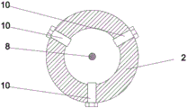
其中:1-敏感芯片,2-封装外壳,3-准直器内限位块,4-螺纹准直器,5-螺纹固定器,6-外固定环,601-让位槽,7-准直器外限位块,8-光纤,9-调节栓固定套壳,10-螺纹调节栓,11-高温胶,12-调节栓定位槽,13-工作调节架,14-光源,15-光功率计,16-光屏。Among them: 1-sensitive chip, 2-packaging shell, 3-inner limit block of collimator, 4-thread collimator, 5-thread fixer, 6-outer fixing ring, 601-give way groove, 7-collimator Straightener outer limit block, 8-optical fiber, 9-adjusting bolt fixing sleeve, 10-threaded adjusting bolt, 11-high temperature glue, 12-adjusting bolt positioning slot, 13-working adjustment frame, 14-light source, 15-light Power meter, 16-light screen.
具体实施方式Detailed ways
为了使本领域的普通技术人员能更好的理解本发明的技术方案,下面结合附图和实施例对本发明的技术方案做进一步的描述。In order to enable those skilled in the art to better understand the technical solution of the present invention, the technical solution of the present invention will be further described below in conjunction with the accompanying drawings and embodiments.
实施例1Example 1
参照附图1-5所示的一种基于光纤F-P腔的MEMS传感器,包括用于封装敏感芯片1的封装外壳2,所述敏感芯片1封装在所述封装外壳2的一端端部,所述封装外壳2远离所述敏感芯片1的一端螺纹连接有螺纹准直器4,所述螺纹准直器4的外侧壁中间段上设有外螺纹,所述封装外壳2远离所述敏感芯片1的一端内侧壁上设有内螺纹,所述螺纹准直器4与所述封装外壳2螺纹连接。A kind of MEMS sensor based on the optical fiber F-P cavity shown in accompanying drawing 1-5, comprises the
所述螺纹准直器4位于所述封装外壳2外的一端固设有准直器外限位块7,所述螺纹准直器4与所述外限位块7为整体结构,且所述封装外壳2远离所述敏感芯片1的一端与所述准直器外限位块7之间设有螺纹固定器5,所述螺纹固定器5的外侧壁上设有外螺纹,内侧壁为光滑设计,可套设在所述螺纹准直器4外,且可沿着所述螺纹准直器4的长轴方向滑动;所述封装外壳2和所述准直器外限位块7的外径相同;所述封装外壳2的内侧壁上固设有一圈用于对螺纹准直器4前端位置进行限位的准直器内限位块3,所述准直器内限位块3的作用是为了避免螺纹准直器4过度向内顶到敏感芯片1;所述螺纹准直器4的中心贯穿设有光纤8。One end of the threaded
所述封装外壳2、螺纹固定器5和准直器外限位块7外还套设有同一个外固定环6,所述外固定环6的内侧壁上设有与螺纹固定器5外侧壁上的外螺纹相匹配的内螺纹,从而使得所述外固定环6与所述螺纹固定器5之间螺纹连接,所述外固定环6还通过高温胶11与所述封装外壳2和准直器外限位块7固定;为了减少准直器外限位块7与螺纹固定器5之间的冲击,在所述准直器外限位块7靠近螺纹准直器4的一侧设有橡胶垫,橡胶垫还可以作为衬底起到密封作用。The same
所述封装外壳2上沿周向对称设有三个调节栓定位槽12,三个调节栓定位槽12所在的圆面位于螺纹准直器4设有外螺纹部分的前方,每个所述调节栓定位槽12中均螺纹连接有螺纹调节栓10,所述螺纹调节栓10外均设有调节栓固定套壳9,每个所述调节栓固定套壳9也通过高温胶11与所述封装外壳2的外侧壁固定。The
为了避免调节栓固定套壳9对外固定环6造成阻挡,在所述外固定环6的内侧壁上开设有三个与所述调节栓固定套壳9相匹配的让位槽601,便于将外固定环6从螺纹准直器4的前端套设至螺纹准直器4的后端。In order to prevent the adjusting
优选的,所述螺纹准直器4为陶瓷材料,陶瓷热膨胀系数小,且可自带润滑增加连接处的可靠性和强度。Preferably, the threaded
实施例2Example 2
实施例二提供一种实施例一中所述的基于光纤F-P腔的MEMS传感器的封装方法,具体包括以下步骤,
S1:将封装有敏感芯片1的封装外壳2和螺纹准直器4分别固定在一对水平放置的工作调节架13上,封装外壳2和螺纹准直器4开始的距离应该以设计的工作距离为准,通过调节两个工作调节架13的位置进行对光;放置光屏16与两个工作调节架13处于同一直线上,如附图6所述;S1: Fix the
S2:将光源14与螺纹准直器4进行连接,调节放置有螺纹准直器4的工作调节架13,使螺纹准直器4发出的光到达光屏16的中心点位;S2: Connect the
将可见光的光源14与螺纹准直器4连接,以确定敏感芯片1的返回光位置,对光时,主要利用光的反射定律。首先保证螺纹准直器4出射光点打到敏感芯片1正中间,此时传感器灵敏度最高,然后根据敏感芯片1返回光的位置进行后续调整。Connect the
然后,从螺纹准直器4看向敏感芯片1,当光点位置在光屏16偏左(右)时,说明在XOY平面上螺纹准直器4入射光角度偏大,通过将螺纹准直器4对应的工作调节架13沿Z轴向外(里)进给,同时调整该工作调节架13沿Y轴方向向里(外)进给,可将偏离的光点调整到中心。Then, looking at the sensitive chip 1 from the threaded
S3:将螺纹准直器4与光功率计15连接,通过光功率计15对光源14发出的光经过敏感芯片1后的返回光,再经过螺纹准直器4和光纤8到达光功率计15的光强进行检测,然后对螺纹准直器4对应的工作调节架13进行精确调节,确定返回光强最大处,也即螺纹准直器4的最佳工作距离;S3: Connect the threaded
步骤S2中使用可见光初步确定螺纹准直器4和封装外壳2的相对位置后,将螺纹准直器4与光功率计15连接,通过光功率计15对光源14发出的光经过敏感芯片1后的返回光,再经过螺纹准直器4和光纤8到达光功率计15的光强进行检测,当返回光功率最大时信号最佳。In step S2, after initially determining the relative positions of the threaded
一定距离下调整完毕后,调节工作调节架13的位置,改变敏感芯片1与螺纹准直器4的相对距离,继续微调,得到不同距离的返回光功率值,最大值对应的距离即为螺纹准直器4最佳工作距离。After the adjustment at a certain distance, adjust the position of the working
如果没有达到最大或光功率无变化需要重复进行可见光对光或检查检测系统是否有效工作。If it does not reach the maximum or the optical power does not change, it is necessary to repeat the visible light alignment or check whether the detection system is working effectively.
S4:将螺纹准直器4与封装外壳2进行连接固定;S4: Connect and fix the threaded
具体的,S401:将螺纹固定器5套设在螺纹准直器4上,调节放置有螺纹准直器4的工作调节架13,将螺纹准直器4螺旋拧入封装外壳2内;此处需要说明的是,工作调节架13上设有旋钮,可对螺纹准直器4在X轴、Y轴和Z轴上的位置进行调节,该工作调节架13为现有技术,其具体结构本申请中不做赘述。Specifically, S401: Set the threaded
在进行螺纹准直器4与封装外壳2的连接时,螺纹准直器4接红光,用于观察出光点位置。传感器封装时注意使用红光观察调节光点位置,尽量保证光点位于敏感芯片1的中心,保证传感器性能。调整其相对位置,保证螺纹准直器4与封装外壳2内孔处于同一轴线上,即光通过螺纹准直器4和封装外壳2,且能在光屏16上看到清晰明亮的红色光点(光通过封装外壳到达敏感芯片顶部时发生了光的干涉现象),且光点能够从封装外壳2的内孔中心射出。When connecting the threaded
S402:当螺纹准直器4到达最大限位处时,将螺纹固定器5与准直器外限位块7紧密贴合;S402: When the threaded
S403:将外固定环6从封装外壳2远离螺纹准直器4的一端套入,并套设在螺纹固定器5和准直器外限位块7上,通过高温胶11进行加固;S403: Insert the
S404:再次观察光功率计15,若无法满足性能要求,则在调节栓定位槽12中插设螺纹调节栓10对螺纹准直器4的光路进行对准,得到光强最大点后在螺纹调节栓10外套入调节栓固定套壳9,并通过高温胶11进行固定,完成封装。S404: Observe the
完成封装之后,还需要分析传感器的压力性能及耐温性能,如无法满足性能要求需要重新完成上述封装过程,确保传感器可以高效工作。After the packaging is completed, the pressure performance and temperature resistance performance of the sensor need to be analyzed. If the performance requirements cannot be met, the above packaging process needs to be completed again to ensure that the sensor can work efficiently.
以上显示和描述了本发明的基本原理、主要特征和本发明的优点。本行业的技术人员应该了解,本发明不受上述实施例的限制,上述实施例和说明书中描述的只是说明本发明的原理,在不脱离本发明精神和范围的前提下,本发明还会有各种变化和改进,这些变化和改进都落入要求保护的本发明范围内。本发明要求保护范围由所附的权利要求书及其等效物界定。The basic principles, main features and advantages of the present invention have been shown and described above. Those skilled in the industry should understand that the present invention is not limited by the above-mentioned embodiments. What are described in the above-mentioned embodiments and the description only illustrate the principle of the present invention. Without departing from the spirit and scope of the present invention, the present invention will also have Variations and improvements are possible, which fall within the scope of the claimed invention. The protection scope of the present invention is defined by the appended claims and their equivalents.
Claims (2)
Priority Applications (1)
| Application Number | Priority Date | Filing Date | Title |
|---|---|---|---|
| CN202310434277.4A CN116164781B (en) | 2023-04-21 | 2023-04-21 | A MEMS sensor based on optical fiber F-P cavity and its packaging method |
Applications Claiming Priority (1)
| Application Number | Priority Date | Filing Date | Title |
|---|---|---|---|
| CN202310434277.4A CN116164781B (en) | 2023-04-21 | 2023-04-21 | A MEMS sensor based on optical fiber F-P cavity and its packaging method |
Publications (2)
| Publication Number | Publication Date |
|---|---|
| CN116164781A CN116164781A (en) | 2023-05-26 |
| CN116164781B true CN116164781B (en) | 2023-07-07 |
Family
ID=86416624
Family Applications (1)
| Application Number | Title | Priority Date | Filing Date |
|---|---|---|---|
| CN202310434277.4A Active CN116164781B (en) | 2023-04-21 | 2023-04-21 | A MEMS sensor based on optical fiber F-P cavity and its packaging method |
Country Status (1)
| Country | Link |
|---|---|
| CN (1) | CN116164781B (en) |
Citations (20)
| Publication number | Priority date | Publication date | Assignee | Title |
|---|---|---|---|---|
| CN102866593A (en) * | 2012-09-17 | 2013-01-09 | 上海华力微电子有限公司 | Device for monitoring stability of optical path of photoetching equipment |
| CN103258580A (en) * | 2012-02-08 | 2013-08-21 | 西门子公司 | Contour collimator and adaptive filter and associated method |
| CN203551100U (en) * | 2013-09-29 | 2014-04-16 | 中国电子科技集团公司第二十七研究所 | Novel Fabry-Perot interference-type MEMS sound wave sensor |
| CN104501729A (en) * | 2014-12-04 | 2015-04-08 | 中国科学院上海微系统与信息技术研究所 | Optical fiber F-P strain gauge based on MEMS technology and formation method thereof |
| CN106154540A (en) * | 2016-06-30 | 2016-11-23 | 武汉光迅科技股份有限公司 | A kind of rotary mirror type MEMS variable optical attenuator |
| CN106153978A (en) * | 2016-06-20 | 2016-11-23 | 天津大学 | Flow velocity based on optical fiber MEMS method amber microcavity test device and method of testing |
| CN106672887A (en) * | 2016-12-29 | 2017-05-17 | 武汉理工大学 | Vibration acceleration sensing device based on silicon carbide optical fiber F-P resonant cavity |
| CN107162589A (en) * | 2017-07-17 | 2017-09-15 | 黄石晨信光电股份有限公司 | A kind of complete ceramic wavelength division multiplexer and preparation method thereof |
| CN207216081U (en) * | 2017-08-31 | 2018-04-10 | 福州高意通讯有限公司 | A kind of small optical switch encapsulating structure |
| CN108007595A (en) * | 2017-11-21 | 2018-05-08 | 西北工业大学 | A kind of sonde-type thin-film thermocouple temperature sensor and preparation method thereof |
| CN111707404A (en) * | 2020-05-28 | 2020-09-25 | 西安交通大学 | A kind of high temperature resistant silicon carbide pressure sensor and preparation method thereof |
| CN112629426A (en) * | 2020-11-20 | 2021-04-09 | 西北工业大学 | Optical fiber strain sensing device |
| CN112649144A (en) * | 2020-12-17 | 2021-04-13 | 中国电子科技集团公司第十三研究所 | High-temperature-resistant pressure sensor packaging structure based on optical detection |
| CN213338191U (en) * | 2020-08-17 | 2021-06-01 | 维什激光科技(苏州)有限公司 | Double-layer thread alignment adjusting mechanism |
| CN112903154A (en) * | 2021-04-01 | 2021-06-04 | 重庆拜安科技有限公司 | Extrinsic optical fiber Fabry-Perot interference pressure sensor |
| CN113229839A (en) * | 2021-05-29 | 2021-08-10 | 西北工业大学 | Linear collimator matched with linear array X-ray detector of bone densitometer |
| CN114486019A (en) * | 2022-01-12 | 2022-05-13 | 西北工业大学 | Optical fiber Fabry-Perot pressure sensor for eliminating third-cavity interference and MEMS manufacturing method |
| CN114739571A (en) * | 2022-04-21 | 2022-07-12 | 西安近代化学研究所 | Packaging device of MEMS pressure sensor |
| CN115196582A (en) * | 2022-07-13 | 2022-10-18 | 西安交通大学 | High-pressure-resistant MEMS pressure sensor packaging structure and packaging method |
| CN115342954A (en) * | 2022-08-23 | 2022-11-15 | 西安交通大学 | MEMS high-temperature-resistant pressure sensor based on optical-mechanical-electrical-thermal multi-physical-field coupling |
Family Cites Families (3)
| Publication number | Priority date | Publication date | Assignee | Title |
|---|---|---|---|---|
| US6654517B2 (en) * | 2001-02-21 | 2003-11-25 | Vitesse Semiconductor Corporation | Optical devices engaged to fibers with angle-polished facets |
| US7511823B2 (en) * | 2004-12-21 | 2009-03-31 | Halliburton Energy Services, Inc. | Fiber optic sensor |
| US7559701B2 (en) * | 2007-03-19 | 2009-07-14 | General Electric Company | High-temperature pressure sensor and method of assembly |
-
2023
- 2023-04-21 CN CN202310434277.4A patent/CN116164781B/en active Active
Patent Citations (20)
| Publication number | Priority date | Publication date | Assignee | Title |
|---|---|---|---|---|
| CN103258580A (en) * | 2012-02-08 | 2013-08-21 | 西门子公司 | Contour collimator and adaptive filter and associated method |
| CN102866593A (en) * | 2012-09-17 | 2013-01-09 | 上海华力微电子有限公司 | Device for monitoring stability of optical path of photoetching equipment |
| CN203551100U (en) * | 2013-09-29 | 2014-04-16 | 中国电子科技集团公司第二十七研究所 | Novel Fabry-Perot interference-type MEMS sound wave sensor |
| CN104501729A (en) * | 2014-12-04 | 2015-04-08 | 中国科学院上海微系统与信息技术研究所 | Optical fiber F-P strain gauge based on MEMS technology and formation method thereof |
| CN106153978A (en) * | 2016-06-20 | 2016-11-23 | 天津大学 | Flow velocity based on optical fiber MEMS method amber microcavity test device and method of testing |
| CN106154540A (en) * | 2016-06-30 | 2016-11-23 | 武汉光迅科技股份有限公司 | A kind of rotary mirror type MEMS variable optical attenuator |
| CN106672887A (en) * | 2016-12-29 | 2017-05-17 | 武汉理工大学 | Vibration acceleration sensing device based on silicon carbide optical fiber F-P resonant cavity |
| CN107162589A (en) * | 2017-07-17 | 2017-09-15 | 黄石晨信光电股份有限公司 | A kind of complete ceramic wavelength division multiplexer and preparation method thereof |
| CN207216081U (en) * | 2017-08-31 | 2018-04-10 | 福州高意通讯有限公司 | A kind of small optical switch encapsulating structure |
| CN108007595A (en) * | 2017-11-21 | 2018-05-08 | 西北工业大学 | A kind of sonde-type thin-film thermocouple temperature sensor and preparation method thereof |
| CN111707404A (en) * | 2020-05-28 | 2020-09-25 | 西安交通大学 | A kind of high temperature resistant silicon carbide pressure sensor and preparation method thereof |
| CN213338191U (en) * | 2020-08-17 | 2021-06-01 | 维什激光科技(苏州)有限公司 | Double-layer thread alignment adjusting mechanism |
| CN112629426A (en) * | 2020-11-20 | 2021-04-09 | 西北工业大学 | Optical fiber strain sensing device |
| CN112649144A (en) * | 2020-12-17 | 2021-04-13 | 中国电子科技集团公司第十三研究所 | High-temperature-resistant pressure sensor packaging structure based on optical detection |
| CN112903154A (en) * | 2021-04-01 | 2021-06-04 | 重庆拜安科技有限公司 | Extrinsic optical fiber Fabry-Perot interference pressure sensor |
| CN113229839A (en) * | 2021-05-29 | 2021-08-10 | 西北工业大学 | Linear collimator matched with linear array X-ray detector of bone densitometer |
| CN114486019A (en) * | 2022-01-12 | 2022-05-13 | 西北工业大学 | Optical fiber Fabry-Perot pressure sensor for eliminating third-cavity interference and MEMS manufacturing method |
| CN114739571A (en) * | 2022-04-21 | 2022-07-12 | 西安近代化学研究所 | Packaging device of MEMS pressure sensor |
| CN115196582A (en) * | 2022-07-13 | 2022-10-18 | 西安交通大学 | High-pressure-resistant MEMS pressure sensor packaging structure and packaging method |
| CN115342954A (en) * | 2022-08-23 | 2022-11-15 | 西安交通大学 | MEMS high-temperature-resistant pressure sensor based on optical-mechanical-electrical-thermal multi-physical-field coupling |
Non-Patent Citations (4)
| Title |
|---|
| A novel method for the manufacture of MEMS devices with large exposed area based on SOI wafers;Jianbing Xie 等;2009 4th IEEE International Conference on Nano/Micro Engineered and Molecular Systems;全文 * |
| High-sensitivity photonic crystal diaphragm based sapphire Fabry-Perot acoustic sensor for high-temperature applications;Jiayan Wang 等;2020 IEEE SENSORS;全文 * |
| 光楔式光纤法布里-珀罗传感器相关干涉信号特性分析;陈青青 等;激光与光电子学进展;第55卷(第11期);全文 * |
| 基于SOI的硅微谐振式压力传感器芯片制作;马志波 等;传感技术学报;第25卷(第2期);全文 * |
Also Published As
| Publication number | Publication date |
|---|---|
| CN116164781A (en) | 2023-05-26 |
Similar Documents
| Publication | Publication Date | Title |
|---|---|---|
| CN103557985B (en) | A kind of differential pressure method for sensing and sensor thereof | |
| CN103557984B (en) | A kind of method for packing of differential pressure pick-up probe and structure | |
| CN102062635A (en) | Laser power monitoring device | |
| CN203551182U (en) | Packaging structure of differential pressure probe | |
| CN201926504U (en) | Laser power monitoring device | |
| CN110879061B (en) | A moisture-proof and vibration-resistant frameless optical fiber gyroscope | |
| CN116164781B (en) | A MEMS sensor based on optical fiber F-P cavity and its packaging method | |
| CN106154540A (en) | A kind of rotary mirror type MEMS variable optical attenuator | |
| CN109768470A (en) | A kind of fiber grating feedback device for cavity semiconductor | |
| CN102565496A (en) | Two-way transmission optical current sensor | |
| CN117538563B (en) | Full-rigid packaging high-temperature-resistant optical fiber Fabry-Perot cavity acceleration sensor and assembly method thereof | |
| CN203551183U (en) | Reflective optical-fiber-bundle differential pressure sensor with intensity compensation | |
| CN108663158A (en) | Push-pull type optical fiber differential pressure pickup | |
| CN103557986B (en) | A kind of differential pressure pick-up intensity compensation method and device | |
| CN109612956A (en) | A kind of optical correction's chip for the residual detection system of agriculture | |
| CN204479799U (en) | A kind of array collimator | |
| CN101598774B (en) | Metallization packaged magneto-optical sensor | |
| US7593104B2 (en) | Method for manufacturing optical module, positioning apparatus, evaluation method and evaluation apparatus for evaluating optical module | |
| KR101412212B1 (en) | Optical wave guide | |
| CN203551181U (en) | Intensity compensation device of differential pressure transducer | |
| CN211262252U (en) | Damp-proof and vibration-proof off-skeleton fiber optic gyroscope | |
| CN204613454U (en) | The semiconductor optical device that based semiconductor laser instrument is integrated | |
| US20060197012A1 (en) | Shear and pressure/transverse strain fiber grating sensors | |
| CN201417303Y (en) | Magneto-optic sensors in metallized packages | |
| CN220773299U (en) | Spectroscopic detector and optical fiber communication system |
Legal Events
| Date | Code | Title | Description |
|---|---|---|---|
| PB01 | Publication | ||
| PB01 | Publication | ||
| SE01 | Entry into force of request for substantive examination | ||
| SE01 | Entry into force of request for substantive examination | ||
| GR01 | Patent grant | ||
| GR01 | Patent grant |