CN116149087A - Optical device - Google Patents
Optical device Download PDFInfo
- Publication number
- CN116149087A CN116149087A CN202211272738.4A CN202211272738A CN116149087A CN 116149087 A CN116149087 A CN 116149087A CN 202211272738 A CN202211272738 A CN 202211272738A CN 116149087 A CN116149087 A CN 116149087A
- Authority
- CN
- China
- Prior art keywords
- optical
- optical waveguide
- electro
- layer
- substrate
- Prior art date
- Legal status (The legal status is an assumption and is not a legal conclusion. Google has not performed a legal analysis and makes no representation as to the accuracy of the status listed.)
- Pending
Links
Images


Classifications
-
- G—PHYSICS
- G02—OPTICS
- G02F—OPTICAL DEVICES OR ARRANGEMENTS FOR THE CONTROL OF LIGHT BY MODIFICATION OF THE OPTICAL PROPERTIES OF THE MEDIA OF THE ELEMENTS INVOLVED THEREIN; NON-LINEAR OPTICS; FREQUENCY-CHANGING OF LIGHT; OPTICAL LOGIC ELEMENTS; OPTICAL ANALOGUE/DIGITAL CONVERTERS
- G02F1/00—Devices or arrangements for the control of the intensity, colour, phase, polarisation or direction of light arriving from an independent light source, e.g. switching, gating or modulating; Non-linear optics
- G02F1/01—Devices or arrangements for the control of the intensity, colour, phase, polarisation or direction of light arriving from an independent light source, e.g. switching, gating or modulating; Non-linear optics for the control of the intensity, phase, polarisation or colour
- G02F1/03—Devices or arrangements for the control of the intensity, colour, phase, polarisation or direction of light arriving from an independent light source, e.g. switching, gating or modulating; Non-linear optics for the control of the intensity, phase, polarisation or colour based on ceramics or electro-optical crystals, e.g. exhibiting Pockels effect or Kerr effect
- G02F1/035—Devices or arrangements for the control of the intensity, colour, phase, polarisation or direction of light arriving from an independent light source, e.g. switching, gating or modulating; Non-linear optics for the control of the intensity, phase, polarisation or colour based on ceramics or electro-optical crystals, e.g. exhibiting Pockels effect or Kerr effect in an optical waveguide structure
-
- G—PHYSICS
- G02—OPTICS
- G02F—OPTICAL DEVICES OR ARRANGEMENTS FOR THE CONTROL OF LIGHT BY MODIFICATION OF THE OPTICAL PROPERTIES OF THE MEDIA OF THE ELEMENTS INVOLVED THEREIN; NON-LINEAR OPTICS; FREQUENCY-CHANGING OF LIGHT; OPTICAL LOGIC ELEMENTS; OPTICAL ANALOGUE/DIGITAL CONVERTERS
- G02F1/00—Devices or arrangements for the control of the intensity, colour, phase, polarisation or direction of light arriving from an independent light source, e.g. switching, gating or modulating; Non-linear optics
- G02F1/01—Devices or arrangements for the control of the intensity, colour, phase, polarisation or direction of light arriving from an independent light source, e.g. switching, gating or modulating; Non-linear optics for the control of the intensity, phase, polarisation or colour
- G02F1/03—Devices or arrangements for the control of the intensity, colour, phase, polarisation or direction of light arriving from an independent light source, e.g. switching, gating or modulating; Non-linear optics for the control of the intensity, phase, polarisation or colour based on ceramics or electro-optical crystals, e.g. exhibiting Pockels effect or Kerr effect
- G02F1/0305—Constructional arrangements
- G02F1/0316—Electrodes
-
- G—PHYSICS
- G02—OPTICS
- G02F—OPTICAL DEVICES OR ARRANGEMENTS FOR THE CONTROL OF LIGHT BY MODIFICATION OF THE OPTICAL PROPERTIES OF THE MEDIA OF THE ELEMENTS INVOLVED THEREIN; NON-LINEAR OPTICS; FREQUENCY-CHANGING OF LIGHT; OPTICAL LOGIC ELEMENTS; OPTICAL ANALOGUE/DIGITAL CONVERTERS
- G02F1/00—Devices or arrangements for the control of the intensity, colour, phase, polarisation or direction of light arriving from an independent light source, e.g. switching, gating or modulating; Non-linear optics
- G02F1/01—Devices or arrangements for the control of the intensity, colour, phase, polarisation or direction of light arriving from an independent light source, e.g. switching, gating or modulating; Non-linear optics for the control of the intensity, phase, polarisation or colour
- G02F1/21—Devices or arrangements for the control of the intensity, colour, phase, polarisation or direction of light arriving from an independent light source, e.g. switching, gating or modulating; Non-linear optics for the control of the intensity, phase, polarisation or colour by interference
- G02F1/212—Mach-Zehnder type
-
- G—PHYSICS
- G02—OPTICS
- G02F—OPTICAL DEVICES OR ARRANGEMENTS FOR THE CONTROL OF LIGHT BY MODIFICATION OF THE OPTICAL PROPERTIES OF THE MEDIA OF THE ELEMENTS INVOLVED THEREIN; NON-LINEAR OPTICS; FREQUENCY-CHANGING OF LIGHT; OPTICAL LOGIC ELEMENTS; OPTICAL ANALOGUE/DIGITAL CONVERTERS
- G02F1/00—Devices or arrangements for the control of the intensity, colour, phase, polarisation or direction of light arriving from an independent light source, e.g. switching, gating or modulating; Non-linear optics
- G02F1/01—Devices or arrangements for the control of the intensity, colour, phase, polarisation or direction of light arriving from an independent light source, e.g. switching, gating or modulating; Non-linear optics for the control of the intensity, phase, polarisation or colour
- G02F1/21—Devices or arrangements for the control of the intensity, colour, phase, polarisation or direction of light arriving from an independent light source, e.g. switching, gating or modulating; Non-linear optics for the control of the intensity, phase, polarisation or colour by interference
- G02F1/225—Devices or arrangements for the control of the intensity, colour, phase, polarisation or direction of light arriving from an independent light source, e.g. switching, gating or modulating; Non-linear optics for the control of the intensity, phase, polarisation or colour by interference in an optical waveguide structure
- G02F1/2255—Devices or arrangements for the control of the intensity, colour, phase, polarisation or direction of light arriving from an independent light source, e.g. switching, gating or modulating; Non-linear optics for the control of the intensity, phase, polarisation or colour by interference in an optical waveguide structure controlled by a high-frequency electromagnetic component in an electric waveguide structure
Landscapes
- Physics & Mathematics (AREA)
- Nonlinear Science (AREA)
- General Physics & Mathematics (AREA)
- Optics & Photonics (AREA)
- Chemical & Material Sciences (AREA)
- Engineering & Computer Science (AREA)
- Ceramic Engineering (AREA)
- Crystallography & Structural Chemistry (AREA)
- Electromagnetism (AREA)
- Optical Modulation, Optical Deflection, Nonlinear Optics, Optical Demodulation, Optical Logic Elements (AREA)
- Optical Integrated Circuits (AREA)
Abstract
一种光器件包括基板、层压在基板的一个表面上的第一包覆层、以及形成在第一包覆层中的位于基板的相对侧的第一包覆层中的第一光波导。该光器件还包括层压在第一包覆层的位于基板的相对侧的表面上的电光晶体层以及在电光晶体层的位于第一包覆层的相对侧的表面上由电光晶体层形成的第二光波导。该光器件还包括层压在电光晶体层的位于第一包覆层的相对侧的表面上的第二包覆层。

An optical device includes a substrate, a first cladding layer laminated on one surface of the substrate, and a first optical waveguide formed in the first cladding layer on an opposite side of the substrate. The optical device further includes an electro-optic crystal layer laminated on the surface of the first cladding layer on the opposite side of the substrate, and an electro-optic crystal layer formed of the electro-optic crystal layer on the surface of the electro-optic crystal layer on the opposite side of the first cladding layer. second optical waveguide. The optical device further includes a second cladding layer laminated on the surface of the electro-optic crystal layer on the opposite side of the first cladding layer.
Description
技术领域technical field
本文讨论的实施方式涉及光器件。Embodiments discussed herein relate to optical devices.
背景技术Background technique
硅光子组件由于芯层与包层之间的折射率差大而能够将光强烈地约束在微小区域内,因此可以有效地实现诸如光调制器、光接收元件、相位控制元件或偏振复用器/解复用器之类的各种硅光元件的小型化和高集成度。然而,普通的硅光调制器例如是具有掺杂PN结的载流子控制型,因此存在进一步扩展调制带宽的问题。Due to the large refractive index difference between the core layer and the cladding layer, silicon photonic components can strongly confine light in a small area, so it can effectively realize such as light modulator, light receiving element, phase control element or polarization multiplexer Miniaturization and high integration of various silicon photonic components such as /demultiplexers. However, a common silicon optical modulator is, for example, a carrier-controlled type with a doped PN junction, so there is a problem of further extending the modulation bandwidth.
为了解决该问题,例如,使用具有电光效应的诸如铌酸锂(LiNbO3:LN)之类的电光晶体的光调制器能够扩展调制带宽并防止吸收损失,使得可以实现高性能的光调制器。然而,将除了光调制器之外的诸如光接收元件、相位控制元件或偏振复用器/解复用器之类的硅光元件集成到电光晶体中是很困难的。To solve this problem, for example, an optical modulator using an electro-optic crystal such as lithium niobate (LiNbO 3 : LN) having an electro-optic effect can expand the modulation bandwidth and prevent absorption loss, so that a high-performance optical modulator can be realized. However, it is difficult to integrate silicon optical elements such as light receiving elements, phase control elements, or polarization multiplexers/demultiplexers other than optical modulators into electro-optic crystals.
因此,近年来,其中组合有硅光子组件和具有电光效应的晶体的混合光器件受到关注。在混合光器件中,需要实现硅光子组件的高集成度和具有电光效应的晶体的高调制特性的光器件。Therefore, in recent years, hybrid optical devices in which silicon photonic components and crystals having electro-optical effects are combined have attracted attention. Among hybrid optical devices, optical devices that achieve high integration of silicon photonic components and high modulation characteristics of crystals with electro-optical effects are required.
在传统光器件中,具有电光效应的电光晶体层层压在预先形成的硅光子组件中的缓冲层上,由电光晶体制成的光波导形成在电光晶体层上,并且包覆层层压在电光晶体层上。此外,电极布置在包覆层上,使得能够形成具有电光晶体的光调制器。In conventional optical devices, an electro-optic crystal layer with electro-optic effect is laminated on a buffer layer in a pre-formed silicon photonic component, an optical waveguide made of electro-optic crystal is formed on the electro-optic crystal layer, and a cladding layer is laminated on Electro-optic crystal layer. Furthermore, the electrodes are arranged on the cladding layer, making it possible to form a light modulator with an electro-optic crystal.
专利文献1:美国未审专利申请公开No.2020/0150467Patent Document 1: U.S. Unexamined Patent Application Publication No. 2020/0150467
专利文献2;日本特开2011-102891号公报
在层压在硅光子组件上的电光晶体层上的传统光器件中,第一光波导形成在硅光子组件中的中间层上,并且第二光波导形成在电光晶体层上。然而,如果其上形成有第一光波导的中间层和其上形成有第二光波导的电光晶体层之间的距离过度增大,则将第一光波导和第二光波导光耦合变得困难,从而由于光耦合特性的劣化而发生光损耗。In a conventional optical device laminated on an electro-optic crystal layer on a silicon photonics component, a first optical waveguide is formed on an intermediate layer in the silicon photonics component, and a second optical waveguide is formed on the electro-optic crystal layer. However, if the distance between the intermediate layer on which the first optical waveguide is formed and the electro-optic crystal layer on which the second optical waveguide is formed is excessively increased, optically coupling the first optical waveguide and the second optical waveguide becomes difficult, whereby optical loss occurs due to deterioration of optical coupling characteristics.
因此,本发明的实施方式的一个方面的目的在于提供在保持硅光子元件的高集成度的同时提高耦合效率的光器件等。Therefore, an object of one aspect of the embodiments of the present invention is to provide an optical device or the like that improves coupling efficiency while maintaining a high degree of integration of a silicon photonic element.
发明内容Contents of the invention
根据实施方式的一个方面,一种光器件包括基板、层压在基板的一个表面上的第一包覆层、以及形成在第一包覆层中的位于基板的相对侧的第一包覆层中的第一光波导。光器件还包括层压在第一包覆层的位于基板的相对侧的表面上的电光晶体层、在电光晶体层的位于第一包覆层的相对侧的表面上由电光晶体层形成的第二光波导;以及层压在电光晶体层的位于第一包覆层的相对侧的表面上的第二包覆层。According to an aspect of an embodiment, an optical device includes a substrate, a first cladding layer laminated on one surface of the substrate, and a first cladding layer formed in the first cladding layer on an opposite side of the substrate. The first optical waveguide in . The optical device further includes an electro-optic crystal layer laminated on a surface of the first cladding layer on an opposite side of the substrate, a second electro-optic crystal layer formed of the electro-optic crystal layer on a surface of the electro-optic crystal layer on an opposite side of the first cladding layer. two optical waveguides; and a second cladding layer laminated on the surface of the electro-optic crystal layer on the opposite side of the first cladding layer.
附图说明Description of drawings
图1是例示了根据本实施方式的光器件的构造的示例的示意性平面图;FIG. 1 is a schematic plan view illustrating an example of the configuration of an optical device according to the present embodiment;
图2是例示了沿图1中的线A-A切割的截面部的示例的示意性截面图;FIG. 2 is a schematic cross-sectional view illustrating an example of a cross-sectional portion cut along line A-A in FIG. 1;
图3是例示了沿图1中的线B-B切割的截面部的示例的示意性截面图;3 is a schematic cross-sectional view illustrating an example of a cross-sectional portion cut along line B-B in FIG. 1;
图4是例示了沿图1中的线C-C切割的截面部(马赫-曾德尔(Mach-Zehnder)干涉仪)的示例的示意性截面图;4 is a schematic cross-sectional view illustrating an example of a cross-sectional portion (Mach-Zehnder (Mach-Zehnder) interferometer) cut along line C-C in FIG. 1;
图5是例示了沿图1中的线D-D切割的截面部(相位控制元件)的示例的示意性截面图;5 is a schematic cross-sectional view illustrating an example of a cross-sectional portion (phase control element) cut along line D-D in FIG. 1;
图6是例示了沿图1中的线E-E切割的截面部(光接收元件)的示例的示意性截面图;6 is a schematic cross-sectional view illustrating an example of a cross-sectional portion (light-receiving element) cut along line E-E in FIG. 1;
图7是例示了制造光器件的工序的示例的流程图;7 is a flowchart illustrating an example of a process of manufacturing an optical device;
图8A是例示了硅光子组件的构造示例的示意性截面图;8A is a schematic cross-sectional view illustrating a configuration example of a silicon photonics assembly;
图8B是例示了附接工序的示例的示意性截面图;8B is a schematic cross-sectional view illustrating an example of an attaching process;
图9A是例示了基板去除工序的示例的示意性截面图;9A is a schematic cross-sectional view illustrating an example of a substrate removal process;
图9B是例示了厚度调整工序和电光晶体层形成工序的示例的示意性截面图;9B is a schematic cross-sectional view illustrating an example of a thickness adjustment process and an electro-optic crystal layer formation process;
图10A是例示了第二光波导形成工序的示例的示意性截面图;10A is a schematic cross-sectional view illustrating an example of a second optical waveguide forming process;
图10B是例示了第二包覆层形成工序、电极形成工序以及通孔形成工序的示例的示意性截面图;10B is a schematic cross-sectional view illustrating an example of a second cladding layer forming process, an electrode forming process, and a via hole forming process;
图11A是例示了光调制器的构造示例的示意性平面图;11A is a schematic plan view illustrating a configuration example of an optical modulator;
图11B是例示了IQ光调制器的构造示例的示意性平面图;11B is a schematic plan view illustrating a configuration example of an IQ optical modulator;
图11C是例示了DP-IQ光调制器的构造示例的示意性平面图;11C is a schematic plan view illustrating a configuration example of a DP-IQ optical modulator;
图11D是例示了光通信装置的构造示例的示意性平面图;11D is a schematic plan view illustrating a configuration example of an optical communication device;
图12是例示了根据比较例的光器件的构造示例的示意性平面图;12 is a schematic plan view illustrating a configuration example of an optical device according to a comparative example;
图13是例示了沿图12中的线A1-A1切割的截面部的示例的示意性截面图;FIG. 13 is a schematic cross-sectional view illustrating an example of a cross-sectional portion cut along line A1-A1 in FIG. 12;
图14是例示了沿图12中的线B1-B1切割的截面部的示例的示意性截面图;FIG. 14 is a schematic cross-sectional view illustrating an example of a cross-sectional portion cut along line B1-B1 in FIG. 12;
图15是例示了沿图12中的线C1-C1切割的截面部(马赫-曾德尔干涉仪)的示例的示意性截面图;15 is a schematic cross-sectional view illustrating an example of a cross-sectional portion (Mach-Zehnder interferometer) cut along line C1-C1 in FIG. 12;
图16是例示了沿图12中的线D1-D1切割的截面部(相位控制元件)的示例的示意性截面图;以及FIG. 16 is a schematic cross-sectional view illustrating an example of a cross-sectional portion (phase control element) cut along line D1-D1 in FIG. 12; and
图17是例示了沿图12中的线E1-E1切割的截面部(光接收元件)的示例的示意性截面图。FIG. 17 is a schematic cross-sectional view illustrating an example of a cross-sectional portion (light receiving element) cut along line E1 - E1 in FIG. 12 .
具体实施方式Detailed ways
[a]比较例[a] Comparative example
图12是例示了根据比较例的光器件100的构造示例的示意性平面图。图12例示的光器件100包括输入单元111、第一光波导102、分支单元112、两个光调制器103、两个相位控制元件104、复用单元113、输出单元114和光接收元件105。FIG. 12 is a schematic plan view illustrating a configuration example of an
输入单元111将来自光源(未示出)的信号光输入至第一光波导102。第一光波导102例如是硅光波导,来自输入单元111的信号光穿过该硅光波导。The
光调制器103例如是LN调制器。光调制器103例如是马赫-曾德尔调制器,其包括分支单元112、两个马赫-曾德尔干涉仪103A和复用单元113,并且根据电信号对来自第一光波导102的分光后的信号光进行光调制。分支单元112将来自第一光波导102的信号光分光为用于两个第一光波导102的光,并将分光后的信号光输出到每个马赫-曾德尔干涉仪103A。每个马赫-曾德尔干涉仪103A包括例如由诸如LN之类的电光晶体制成的第二光波导132A以及电极134。电极134包括信号电极134A和接地电极134B。每个马赫-曾德尔干涉仪103A根据施加到信号电极134A的电信号产生从信号电极134A到接地电极134B的电场,根据电场改变第二光波导132A的光折射率,并根据光折射率的变化调整穿过第二光波导132A的光的相位。每个马赫-曾德尔干涉仪103A将已经调整了相位的光输出到每个相位控制元件104。复用单元113复用来自每个相位控制元件104并且经过相移的信号光,并且将复用后的信号光经由第一光波导102输出至输出单元114。The
每个相位控制元件104是使已经通过光调制器103进行光调制的信号光进行移相的硅组件。相位控制元件104经由第一光波导102将已经经过相移的信号光输出给复用单元113。复用单元113复用来自每个相位控制元件104并且已经经过相移的信号光,并将复用后的信号光经由第一光波导102输出给输出单元114。输出单元114连接至光纤(未示出),并且输出来自第一光波导102的复用后的信号光。此外,光接收元件105是将信号光的作为复用单元113的输出的部分转换成电信号的硅组件。Each
此外,例如,提供硅光子组件120,在该硅光子组件120中集成有光器件100中的输入单元111、第一光波导102、分支单元112、两个相位控制元件104、复用单元113、输出单元114和光接收元件105。此外,硅光子组件120是预先形成的组件。In addition, for example, a
图13是例示了沿图12中的线A1-A1切割的截面部的示例的示意性截面图。如图13所示的A1-A1截面部包括硅光子组件120、电光晶体层132和第二包覆层133。FIG. 13 is a schematic cross-sectional view illustrating an example of a cross-sectional portion cut along line A1 - A1 in FIG. 12 . The section A1-A1 shown in FIG. 13 includes a
硅光子组件120包括第一基板121、层压在第一基板121上的第一包覆层124、以及形成在第一包覆层124中的第一光波导102。例如,第一基板121具有小于1000Ωcm的电阻率。第一包覆层124包括层压在第一基板121上的中间层122、形成在中间层122中的第一光波导102、以及层压在中间层122上的缓冲层123。例如,电光晶体层132是层压在硅光子组件120中的缓冲层123上并且由具有电光效应的LN等构成的层。例如,第二包覆层133是层压在电光晶体层132上并且由SiO2等制成的层。The
图14是例示了沿图12中的线B1-B1切割的截面部的示例的示意性截面图。如图14所例示的B1-B1截面部包括第一基板121、中间层122、第一光波导102、缓冲层123、电光晶体层132、形成在电光晶体层132上的第二光波导132A、以及第二包覆层133。第二光波导132A是由电光晶体层132形成的LN光波导。第一光波导102和第二光波导132A光耦合。FIG. 14 is a schematic cross-sectional view illustrating an example of a cross-sectional portion cut along line B1 - B1 in FIG. 12 . The B1-B1 cross section as illustrated in FIG. 14 includes a
图15是例示了沿图12中的线C1-C1切割的截面部(马赫-曾德尔干涉仪103A)的示例的示意性截面图。如图15所示的C1-C1截面部是光调制器103中的马赫-曾德尔干涉仪103A的截面部。C1-C1截面部包括第一基板121、中间层122、缓冲层123、电光晶体层132、第二光波导132A、第二包覆层133、以及形成在第二包覆层133上的电极134。电极134包括信号电极134A和接地电极134B。每个马赫-曾德尔干涉仪103A根据依据施加到信号电极134A的电信号从信号电极134A到接地电极134B产生的电场,来改变第二光波导132A的光折射率,并且根据光折射率的变化,对穿过第二光波导132A的光信号进行光调制。FIG. 15 is a schematic cross-sectional view illustrating an example of a cross-sectional portion (Mach-
图16是例示了沿图12中的线D1-D1(相位控制元件104)切割的截面部的示例的示意性截面图。如图16所例示的D1-D1截面部包括第一基板121、中间层122、第一光波导102、缓冲层123、在缓冲层123中形成于第一光波导102附近的相位控制元件104、电光晶体层132、以及第二包覆层133。在第二包覆层133、电光晶体层132和缓冲层123中形成暴露出相位控制元件104中的金属布线104A2的通孔135。FIG. 16 is a schematic cross-sectional view illustrating an example of a cross-sectional portion cut along line D1 - D1 (phase control element 104 ) in FIG. 12 . The D1-D1 cross section as illustrated in FIG. 16 includes a
相位控制元件104包括:热光加热器104A1,该热光加热器104A1是由TiN等制成的电阻并且布置在第一光波导102上方;以及金属布线104A2,该金属布线104A2电连接到热光加热器104A1并且向热光加热器104A1供应电流。通过使电流从金属布线104A2流到热光加热器104A1,热光加热器104A1产生热量。由于第一光波导102内部的硅折射率因热光加热器104A1的热量而改变,相位控制元件104对穿过第一光波导102内部的光进行移相。The
图17是例示了沿图12中的线E1-E1切割的截面部(光接收元件105)的示例的示意性截面图。如图17所例示的E1-E1截面部包括第一基板121、中间层122、第一光波导102、缓冲层123、在缓冲层123中形成在第一光波导102上的光接收元件105、电光晶体层132、以及第二包覆层133。在第二包覆层133、电光晶体层132和缓冲层123中形成有暴露出光接收元件105中的金属布线105A2的通孔135。FIG. 17 is a schematic cross-sectional view illustrating an example of a cross-sectional portion (light receiving element 105 ) cut along line E1 - E1 in FIG. 12 . The E1-E1 sectional portion illustrated in FIG. 17 includes a
光接收元件105包括:光电转换元件105A1,该光电转换元件105A1由Ge等制成并且布置在第一光波导102上;以及金属布线105A2,该金属布线105A2连接到光电转换元件105A1并输出来自光电转换元件105A1的电信号。光接收元件105将穿过第一光波导102的信号光经由光电转换元件105A1转换为电信号,并且将电信号经由金属布线105A2输出给监视器(未示出)。The
在比较例的光器件100中,电光晶体层132层压在预先形成的硅光子组件120中的缓冲层123上,第二光波导132A形成在电光晶体层132上,并且第二包覆层133层压在电光晶体层132上。此外,电极134布置在第二包覆层133上,使得能够形成具有电光晶体的光调制器103。In the
在层压在硅光子组件120上的电光晶体层132上的光器件100中,第一光波导102形成在硅光子组件120中的中间层122上,并且第二光波导132A形成在电光晶体层132上。然而,例如,当焦点被赋予光接收元件105和相位控制元件104时,如果其上形成有第一光波导102的中间层122与其上形成有第二光波导132A的电光晶体层132之间的距离L1过度增加,则难以进行第一光波导102和第二光波导132A的光耦合,使得由光耦合特性劣化而产生光损失。In the
此外,在光调制器103中,硅光子组件120中的第一基板121的电阻率小于1000Ωcm,使得光调制器103的调制带宽劣化。In addition, in the
因此,需要提供根据本实施方式的光器件,其中可以通过减小其上形成有第二光波导的电光晶体层和形成在中间层上的第一光波导之间的距离来使光耦合性能稳定,并且可以防止光调制器的调制带宽劣化。Therefore, it is necessary to provide the optical device according to the present embodiment, in which the optical coupling performance can be stabilized by reducing the distance between the electro-optic crystal layer on which the second optical waveguide is formed and the first optical waveguide formed on the intermediate layer. , and can prevent the modulation bandwidth of the optical modulator from deteriorating.
下面将参照附图详细描述本申请中公开的光器件等的实施方式。本发明不受以下实施方式的限制。Embodiments of the optical device and the like disclosed in the present application will be described in detail below with reference to the accompanying drawings. The present invention is not limited by the following embodiments.
[b]实施方式[b] Implementation
图1是例示了根据本实施方式的光器件1的示例的示意性平面图。图1所例示的光器件1包括输入单元11、第一光波导2、分支单元12、两个光调制器3、两个相位控制元件4、复用单元13、输出单元14和光接收元件5。FIG. 1 is a schematic plan view illustrating an example of an optical device 1 according to the present embodiment. The optical device 1 illustrated in FIG. 1 includes an
输入单元11将来自光源(未示出)的信号光输入到第一光波导2。第一光波导2例如是来自输入单元11的信号光所穿过的硅光波导。The
光调制器3例如是由具有电光效应的诸如LN之类的晶体制成的LN光调制器。光调制器3例如是马赫-曾德尔调制器,其包括分支单元12、两个马赫-曾德尔干涉仪3A和复用单元13,并且根据电信号对来自第一光波导2的分光信号光进行光调制。分支单元12将来自第一光波导2的信号光分光到两个第一光波导2中,并将分光后的信号光输出给每个马赫-曾德尔干涉仪3A。例如,每个马赫-曾德尔干涉仪3A包括第二光波导32A和电极34。例如,第二光波导32A是LN光波导。电极34包括信号电极34A和接地电极34B。每个马赫-曾德尔干涉仪3A根据施加到信号电极34A的电信号产生从信号电极34A到接地电极34B的电场,根据电场改变第二光波导32A的光折射率,并且根据光折射率的变化调整穿过第二光波导32A的光的相位。每个马赫-曾德尔干涉仪3A向各相位控制元件4输出已经调整了相位的光。复用单元13对来自每个相位控制元件4并且经过了相移的信号光进行复用,并且经由第一光波导2向输出单元14输出复用后的信号光。The
每个相位控制元件4是对已经通过光调制器3进行光调制的信号光进行移相的硅组件。相位控制元件4经由第一光波导2向复用单元13输出已经经过相移的信号光。输出单元14连接到光纤(未示出)并且输出来自第一光波导2的复用后的信号光。此外,光接收元件5是对信号光的作为复用单元13的输出的一部分进行电转换的硅组件。Each
此外,例如,提供硅光子组件20,在该硅光子组件20中集成有光器件1中的输入单元11、第一光波导2、分支单元12、两个相位控制元件4、复用单元13、输出单元14以及光接收元件5。此外,硅光子组件20是预先形成的组件。In addition, for example, a
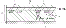
图2是例示了沿图1中的线A1-A1切割的截面部的示例的示意性截面图。如图2所示的A-A截面部包括第二基板31、硅光子组件20A、电光晶体层32和第二包覆层33。硅光子组件20A是去除了第一基板21的硅光子组件20。FIG. 2 is a schematic cross-sectional view illustrating an example of a cross-sectional portion cut along line A1 - A1 in FIG. 1 . The section A-A shown in FIG. 2 includes a
第二基板31是电阻率例如为等于或大于1000Ωcm的基板。第二基板31的厚度例如为1000微米(μm)。此外,第二基板31是由例如硅、LN或石英制成的基板。硅光子组件20包括第一基板21、层压在第一基板21上的第一包覆层24、以及形成在第一包覆层24中的第一光波导2。第一包覆层24由例如SiO2的材料制成。此外,第一光波导2例如是硅波导。第一光波导2例如是肋状波导。第一光波导2是形成在第一包覆层24中的位于第二基板31的相对侧的第一包覆层24中的光波导。The
第一包覆层24包括层压在第一基板21上的中间层22、形成在中间层22上的第一光波导2、以及层压在中间层22上的缓冲层23。缓冲层23是层压在第二基板31的一个表面上的层。中间层22是层压在缓冲层23的位于第二基板31相对侧的一个表面上的层。The
第二基板31处于附接硅光子组件20A中的缓冲层23的状态。换言之,图2所例示的A-A截面部包括第二基板31、层压在第二基板31上的缓冲层23、层压在缓冲层23上并且其中形成有第一光波导2的中间层22、层压在中间层22上的电光晶体层32、以及层压在电光晶体层32上的第二包覆层33。第二包覆层33例如由SiO2制成。第二包覆层33是层压在电光晶体层32的位于第一包覆层24的相对侧的一个表面上的层。The
第一光波导2在第二基板31一侧处形成于中间层22上。电光晶体层32例如是X-切割LN层。LN是折射率通过施加电场而改变并且具有例如大约30pm/V的Pockels(普克尔斯)系数的各向异性材料。电光晶体层32是层压在第二基板31相对侧的第一包覆层24上的层。第二光波导32A是在电光晶体层32的位于第一包覆层24的相对侧的表面上由电光晶体层32形成的光波导。此外,第一光波导2和第二光波导32A具有梯形形状,使得各自的长边隔着中间层22彼此面对。The first
例如,中间层22是由具有比LN更低的光学折射率的SiO2制成的层。第一光波导2与第二光波导32A之间的中间层22的厚度例如为约2μm至6μm。缓冲层23是由SiO2制成并且布置为防止经由第一光波导2传播的光被电极34吸收的层。例如,电光晶体层32的厚度为约0.5μm至3μm。For example, the
图3是例示了沿图1中的线B-B切割的截面部的示例的示意性截面图。如图3所例示的B-B截面部是连接第一光波导2和第二光波导32A的耦合部2A。B-B截面部包括第二基板31、缓冲层23、第一光波导2、中间层22、电光晶体层32、形成在电光晶体层32上的第二光波导32A、以及第二包覆层33。第一光波导2和第二光波导32A光耦合。第一光波导2和第二光波导32A定位为在垂直方向上彼此靠近,并且例如,第一光波导2的宽度被绝热地减小以削弱光约束,使得第一光波导2逐渐与第二光波导32A耦合。此外,形成在中间层22上的第一光波导2和形成在电光晶体层32上的第二光波导32A之间的中间层22的厚度(即,第一光波导2和第二光波导32A之间的距离L)减小。FIG. 3 is a schematic cross-sectional view illustrating an example of a cross-sectional portion cut along line B-B in FIG. 1 . The B-B cross-sectional portion as illustrated in FIG. 3 is the
图4是例示了沿图1中的线C-C切割的截面部(马赫-曾德尔干涉仪3A)的示例的示意性截面图。如图4所示的C-C截面部是光调制器3中的马赫-曾德尔干涉仪3A的截面部。C-C截面部包括第二基板31、缓冲层23、中间层22、电光晶体层32、第二光波导32A、第二包覆层33、以及形成在第二包覆层33上的电极34。FIG. 4 is a schematic cross-sectional view illustrating an example of a cross-sectional portion (Mach-
电极34包括信号电极34A和接地电极34B。例如,信号电极34A是由诸如金、铜之类的金属材料制成的电极,具有2μm至10μm的宽度,并且具有1μm至20μm的厚度。例如,接地电极34B是由诸如金或铜之类的金属材料制成的电极,并且具有等于或大于1μm的厚度。The
如果电光晶体层32是X-切割LN,则通过在水平方向施加电场来改变折射率,并且在第二光波导32A的左右方向上从信号电极34A向接地电极34B施加电场。每个马赫-曾德尔干涉仪3A根据通过向信号电极34A施加电信号而从信号电极34A到接地电极34B施加的电场,来改变第二光波导32A的光折射率,并且根据光折射率的变化,对穿过第二光波导32A的信号光进行光调制。If the electro-
图5是例示了沿图1中的线D-D切割的截面部(相位控制元件4)的示例的示意性截面图。如图5所例示的D-D截面部包括第二基板31、缓冲层23、第一光波导2、中间层22、在缓冲层23中形成于第一光波导2附近的相位控制元件4、电光晶体层32和第二包覆层33。在第二包覆层33、电光晶体层32、中间层22和缓冲层23中形成有暴露出相位控制元件4中的金属布线4A2的通孔35。FIG. 5 is a schematic cross-sectional view illustrating an example of a cross-sectional portion (phase control element 4 ) cut along line D-D in FIG. 1 . The D-D section as illustrated in FIG. 5 includes a
相位控制元件4包括:热光加热器4A1,该热光加热器4A1是由TiN等制成的电阻并布置在第一光波导2附近的位置处;以及金属布线4A2,该金属布线4A2电连接到热光加热器4A1并且向热光加热器4A1供应电流。通过使电流从金属布线4A2流到热光加热器4A1,热光加热器4A1产生热量。由于第一光波导2内部的硅折射率因热光加热器4A1的热量而改变,相位控制元件4对穿过第一光波导2内部的光进行移相。The
图6是例示了沿图1中的线E-E切割的截面部(光接收元件5)的示例的示意性截面图。如图6所示的E-E截面部包括第二基板31、缓冲层23、第一光波导2、中间层22、在缓冲层23中形成于第一光波导2附近的光接收元件5、电光晶体层32、以及第二包覆层33。在第二包覆层33、电光晶体层32、中间层22和缓冲层23中形成有暴露出光接收元件5中的金属布线5A2的通孔35。FIG. 6 is a schematic cross-sectional view illustrating an example of a cross-sectional portion (light-receiving element 5 ) cut along line E-E in FIG. 1 . The E-E cross section shown in FIG. 6 includes a
光接收元件5包括:光电转换元件5A1,该光电转换元件5A1由Ge等制成并布置在第一光波导2附近的位置处;以及金属布线5A2,该金属布线5A2连接到光电转换元件51A,并且输出来自光电转换元件5A1的电信号。光接收元件5将穿过第一光波导2的信号光经由光电转换元件5A1转换为电信号,并将电信号经过金属布线5A2输出给监视器(未示出)。The
图7是例示了制造光器件1的工序的示例的流程图。作为制造工序,执行制备预先形成的硅光子组件20的制备工序(步骤S11)。执行将硅光子组件20反转并且将第二基板31附接到硅光子组件20中的缓冲层23的表面的附接工序(步骤S12)。此外,第二基板31是具有等于或大于1000Ωcm的高电阻率的基板,第二基板的电阻率高于第一基板21的电阻率。FIG. 7 is a flowchart illustrating an example of a procedure of manufacturing the optical device 1 . As a manufacturing process, a manufacturing process of preparing a preformed
在附接第二基板31之后,执行去除硅光子组件20中的第一基板21的去除工序(步骤S13)。执行调整去除了第一基板21的硅光子组件20A中的中间层22的厚度的厚度调整工序(步骤S14)。此外,通过调整中间层22的厚度,在完成时,可以减小电光晶体层32的第二光波导32A与第一光波导2之间的距离L并实现高效率的光耦合。After the
执行将电光晶体层32层压在硅光子组件20A中的已经调整了中间层22的厚度中间层22上的电光晶体层形成工序(步骤S15)。执行在电光晶体层32上形成第二光波导32A的第二光波导形成工序(步骤S16)。An electro-optic crystal layer forming process of laminating the electro-
执行在其上已经形成有第二光波导32A的电光晶体层32上形成第二包覆层33的第二包覆层形成工序(步骤S17)。此外,执行在第二包覆层33上布置电极34的电极形成工序(步骤S18)。此外,在布置电极34之后,执行在第二包覆层33、电光晶体层32和缓冲层23中形成通孔35以暴露出缓冲层23中的相位控制元件4的金属布线4A2和光接收元件5的金属布线5A2的通孔形成工序(步骤S19)。结果,形成如图10B所示的光器件1。A second cladding layer forming process of forming the
在图10B所例示的光器件1中,采用具有比第一基板21更高电阻率的第二基板31,使得可以避免例如光调制器3的调制带宽劣化的情况。此外,在光器件1中,调整中间层22的厚度,并且减小电光晶体层32中的第二光波导32A与第一光波导2之间的距离L,使得可以提高第一光波导2和第二光波导32A之间的光耦合效率。In the optical device 1 illustrated in FIG. 10B , the
图8A是例示了硅光子组件20的构造示例的示意性截面图。硅光子组件20具有第一基板21、中间层22、多个第一光波导2、以及缓冲层23。相位控制元件4和光接收元件5合并到缓冲层23中的任意第一光波导2中。硅光子组件20是预先形成的组件。FIG. 8A is a schematic cross-sectional view illustrating a configuration example of a
图8B是例示了附接工序的示例的示意性截面图。在如图8A所例示的硅光子组件20被上下倒置之后,将第二基板31附接在硅光子组件20的缓冲层23上。Fig. 8B is a schematic cross-sectional view illustrating an example of an attaching process. After the
图9A是例示了基板去除工序的示例的示意性截面图。通过去除第二基板31所附接至的硅光子组件20中的第一基板21,形成如图9A所例示的硅光子组件20A。FIG. 9A is a schematic cross-sectional view illustrating an example of a substrate removal process. By removing the
图9B是例示了厚度调整工序和电光晶体层形成工序的示例的示意性截面图。调整已经去除了第一基板21的硅光子组件20A中的中间层22的厚度。通过调整中间层22的厚度,调整第一光波导2和第二光波导32A之间的距离。此外,在调整中间层22的厚度之后,将电光晶体层32层压在硅光子组件20A的中间层22上。9B is a schematic cross-sectional view illustrating an example of a thickness adjustment process and an electro-optic crystal layer formation process. The thickness of the
图10A是例示了第二光波导形成工序的示例的示意性截面图。在将电光晶体层32层压在硅光子组件20A的中间层22上之后,在电光晶体层32上形成第二光波导32A。FIG. 10A is a schematic cross-sectional view illustrating an example of a second optical waveguide forming process. After the electro-
图10B是例示了第二包覆层形成工序、电极形成工序以及通孔形成工序的示例的示意性截面图。在形成第二光波导32A之后,将第二包覆层33层压在电光晶体层32上。此外,在层压第二包覆层33之后,在马赫-曾德尔干涉仪3A中的其上布置有第二光波导32A的第二包覆层33上布置信号电极34A和接地电极34B。此外,通孔35形成在第二包覆层33、电光晶体层32、中间层22和缓冲层23中,使得硅光子组件20A中的相位控制元件4的金属布线4A2和光接收元件5的金属布线5A2从第二包覆层33暴露出来,从而形成光器件1。10B is a schematic cross-sectional view illustrating an example of a second cladding layer forming process, an electrode forming process, and a via hole forming process. After forming the second
在根据本实施方式的光器件1中,采用具有比第一基板21更高电阻率的第二基板31,使得可以避免例如光调制器3的调制带宽劣化的情况。此外,在光器件1中,调整中间层22的厚度,并且减小电光晶体层32与第一光波导2之间的距离L,使得可以提高第一光波导2和第二光波导32A之间的光耦合效率。In the optical device 1 according to the present embodiment, the
光器件1包括:第一光波导2,该第一光波导2形成在第一包覆层24中的位于第二基板31的相对侧的第一包覆层24中;电光晶体层32,该电光晶体层32层压在第一包覆层24的位于第二基板31的相对侧的表面上;以及第二光波导32A,该第二光波导32A在电光晶体层32的位于第一包覆层24的相对侧的表面上由电光晶体层32形成。结果,电光晶体层32与第一光波导2之间的距离L减小,使得可以提高第一光波导2与第二光波导32A之间的光耦合效率。此外,可以实现在同时使用硅光子学的高集成度和具有电光效应的晶体的高调制特性的同时能够降低损耗并且适合大规模生产的光器件。The optical device 1 includes: a first
在光器件1中,即使使用其中并入了例如相位控制元件4和光接收元件5的硅光子组件20,也可以将LN光调制器3集成在硅光子组件20中,使得可以提供依据要集成的硅元件实现不同功能的光器件1。In the optical device 1, even if the
第一光波导2形成在中间层22的与缓冲层23接触的表面上,并且电光晶体层32层压在中间层22的位于缓冲层23的相反侧的表面上。因此,电光晶体层32和第一光波导2之间的距离L减小,使得可以提高第一光波导2和第二光波导32A之间的光耦合效率。The first
在第一光波导2和第二基板31之间的第一包覆层24中还布置有至少一个硅组件,例如,硅组件4和5。结果,能够保持高集成度。At least one silicon component, eg
每个光调制器3包括电极34,该电极34布置在第二包覆层33的位于电光晶体层32的相对侧的表面上并且将电信号施加到第二光波导32A,并且第二基板31是具有等于或大于1000Ωcm的电阻率的基板。因此,采用具有比第一基板21更高电阻率的第二基板31,使得能够避免例如光调制器3的调制带宽劣化的情况。Each
信号电极34A和接地电极34B布置在第二包覆层33的位于电光晶体层32的相对侧的表面上,以在X切割电光晶体层32时在第二光波导32A中沿水平方向施加电信号。因此,该技术可适用于包括X-切割电光晶体层32的光调制器3。The
此外,为了便于说明,描述了X-切割LN电光晶体层32作为示例,但是该技术适用于使用Z-切割LN电光晶体层32的光器件1。光器件1包括Z-切割LN电光晶体层32、以及沿电光晶体层32的晶轴的X方向或Y方向形成在电光晶体层32上的第二光波导32A。在折射率通过在垂直(Z)方向上施加电场而改变的电光晶体层32的情况下,电光晶体层32将信号电极34A布置在第二光波导32A正上方,以在第二光波导32A的垂直方向上施加电场。在这种情况下,接地电极34B可以嵌入第二包覆层33中。此外,缓冲层23可以形成在第二光波导32A和信号电极34A之间。例如,通过使用SiO2形成缓冲层23,即使信号电极34A位于第二光波导32A正上方,也可以减少传播的光信号的电极吸收损失。Also, for convenience of explanation, the X-cut LN electro-
此外,虽然描述了电光晶体层32作为示例,但是电光晶体的材料不限于LN,并且可应用任何种类的电光晶体。例如,可应用诸如锆钛酸铅(PZT)之类的钙钛矿氧化物、掺镧锆酸铅-钛酸铅(PLZT)或钛酸钡(BaTiO3),并且可以接受适当的改变。此外,PZT的Pockels系数为约110pm/V,PLZT的Pockels系数为约700pm/V,BaTiO3的Pockels系数为约1850pm/V,因此,应用于本发明的电光晶体的Pockels系数是具有在10pm/V至2000pm/V的范围内的系数的材料。Furthermore, although the electro-
此外,已经描述了其中第一光波导2和第二光波导32A是脊状波导的示例,但是实施方式不限于脊状波导,而是该技术适用于例如通道波导。Furthermore, an example has been described in which the first
图11A是例示了合并有光调制器3的光器件1A的示例的示意性平面图。此外,与图1中所例示的光器件1的组件相同的组件由相同的附图标记指代,并且将省略对相同组件和操作的说明。图11A所例示的光器件1A包括光调制器3和两个相位控制元件4。光调制器3包括分支单元12、两个马赫-曾德尔干涉仪3A和复用单元13。例如,每个马赫-曾德尔干涉仪3A的一部分包括第二基板31、缓冲层23、中间层22、第一光波导2、电光晶体层32、第二光波导32A、第二包覆层33和电极34。每个相位控制元件4的一部分包括第二基板31、缓冲层23、中间层22、第一光波导2、相位控制元件4、电光晶体层32和第二包覆层33。因此,在如图11A所例示的合并有光调制器3的光器件1A中,可以保持硅光子的高集成度,提高第一光波导2和第二光波导32A之间的光耦合效率,并且防止调制带宽的劣化。FIG. 11A is a schematic plan view illustrating an example of an
图11B是例示了合并有IQ光调制器3B的光器件1B的示例的示意性平面图。与图11A中所例示的光器件1A的组件相同的组件由相同的附图标记指代,并且将省略对相同构造和操作的说明。图11B所例示的光器件1B中的IQ光调制器3B包括第一分支单元12A、用于同相(I)分量的光调制器3B1、用于正交(Q)分量的光调制器3B2、两个第一相位控制元件4A、以及第一复用单元13A。用于I分量的光调制器3B1对I分量的光信号进行相位调制。用于Q分量的光调制器3B2对Q分量的光信号进行相位调制。用于I分量的光调制器3B1包括分支单元12、两个马赫-曾德尔干涉仪3A1(3A2)和复用单元13。用于Q分量的光调制器3B2包括分支单元12、两个马赫-曾德尔干涉仪3A1(3A2)和复用单元13。FIG. 11B is a schematic plan view illustrating an example of an optical device 1B incorporating an IQ
第一分支单元12A对来自第一光波导2的信号光进行分光,并将分光后的信号光输出到每个IQ光调制器3B。用于I分量的光调制器3B1将在I分量上经过相位调制并且来自光调制器3B1中的复用单元13的信号光输出到第一相位控制元件4A。第一相位控制元件4A对在I分量上已经经过相位调制的信号光进行移相,并且将经过相移的I分量的信号光输出给第一复用单元13A。The first branching
此外,用于Q分量的光调制器3B2将在Q分量上经过相位调制并且来自光调制器3B2中的复用单元13的信号光输出到第一相位控制元件4A。第一相位控制元件4A对在Q分量上已经经过相位调制的信号光进行移相,并且将经过相移后的Q分量的信号光输出到第一复用单元13A。第一复用单元13A对I分量的信号光和Q分量的信号光进行复用,并将复用后的IQ分量的信号光输出到输出单元14。Further, the optical modulator 3B2 for the Q component outputs the signal light that is phase-modulated on the Q component and comes from the multiplexing
例如,马赫-曾德尔干涉仪3A1(3A2)的一部分包括第二基板31、缓冲层23、中间层22、第一光波导2、电光晶体层32、第二光波导32A、第二包覆层33和电极34。相位控制元件4(第一相位控制元件4A)的一部分包括第二基板31、缓冲层23、中间层22、第一光波导2、相位控制元件4(第一相位控制元件4A)、电光晶体层32和第二包覆层33。因此,在如图11B所例示的合并有IQ光调制器3B的光器件1B中,可以保持硅光子的高集成度,提高第一光波导2和第二光波导32A之间的光耦合效率,并且防止调制带宽的劣化。For example, a part of Mach-Zehnder interferometer 3A1 (3A2) includes
图11C是例示了DP-IQ光调制器3C的构造示例的示意性平面图。与图11B所示的光器件1B的组件相同的组件由相同的附图标记指代,并且将省略相同构造和操作的说明。图11C所例示的光器件1C中的DP-IQ光调制器3C包括第二分支单元12B、用于X偏振分量的IQ光调制器3C1、用于Y偏振分量的IQ光调制器3C2、偏振旋转器(PR)15和偏振合束器(PBC)16。FIG. 11C is a schematic plan view illustrating a configuration example of the DP-IQ
第二分支单元12B对来自第一光波导2的信号光进行分光,并将分光后的信号光输出到每个IQ光调制器3C1和3C2。用于X偏振分量的IQ光调制器3C1包括用于X偏振分量的I分量的光调制器3B1和用于X偏振分量的Q分量的光调制器3B2。The second branching
用于X偏振分量的IQ光调制器3C1中的第一复用单元13A将来自用于I分量的光调制器3B1中的复用单元13的X偏振分量的I分量的信号光和来自用于Q分量的光调制器3B2中的复用单元13的X偏振分量的Q分量的信号光进行复用,并将X偏振分量的IQ分量的信号光输出给PBC 16。The
用于Y偏振的IQ光调制器3C2中的第一复用单元13A将来自用于I分量的光调制器3B2中的复用单元13的Y偏振分量的I分量的信号光和来自用于Q分量的光调制器3B2中的复用单元13的Y偏振分量的Q分量的信号光进行复用,并将Y偏振分量的IQ分量的信号光输出给PR 15。PR 15对Y偏振分量的IQ分量的信号光进行偏振旋转,并将经过偏振旋转的Y偏振分量的IQ分量的信号光输出给PBC 16。PBC16将X偏振分量的IQ分量的信号光和经偏振旋转的Y偏振分量的IQ分量的信号光进行复用,并且将复用后的XY偏振分量的信号光输出至输出单元。The
例如,DP-IQ光调制器3C中的马赫-曾德尔干涉仪3A1(3A2)的一部分包括第二基板31、缓冲层23、中间层22、第一光波导2、电光晶体层32、第二光波导32A、第二包覆层33和电极34。相位控制元件4(第一相位控制元件4A)的一部分包括第二基板31、缓冲层23、中间层22、第一光波导2、相位控制元件4(第一相位控制元件4A)、电光晶体层32和第二包覆层33。此外,PR 15和PBC 16中的每一个的一部分包括第二基板31、缓冲层23、中间层22、第一光波导2、PR 15、PBC 16、电光晶体层32和第二包覆层33。因此,在如图11C所例示的合并有DP-IQ光调制器3C的光器件1C中,可以保持硅光子的高集成度,提高第一光波导2和第二光波导32A之间的光耦合效率,并且防止调制带宽的劣化。For example, a part of the Mach-Zehnder interferometer 3A1 (3A2) in the DP-IQ
图11D是例示了光通信装置1D的构造示例的示意性平面图。此外,与图11C所例示的DP-IQ光调制器3C的组件相同的组件由相同的附图标记指代,并且将省略对相同构造和操作的说明。图11D所例示的光通信装置1D包括DP-IQ光调制器3C、第三分支单元12C、光接收输入单元41、偏振分束器(PBS)42、PR 43、第一光混合电路44A(44)、第二光混合电路44B(44)、四个光接收元件5A和四个光接收元件5B。FIG. 11D is a schematic plan view illustrating a configuration example of the
第三分支单元12C经由输入单元11对来自光源(未示出)的本地光进行分光,并将分光后的光输出给DP-IQ光调制器3C和每个混合电路44。光接收输入单元41接受来自光纤(未示出)的接收光的输入。PBS 42将来自光接收输入单元41的光分割成X偏振接收光和Y偏振接收光,将X偏振接收光输出至第一光混合电路44A,并且将Y偏振接收光输出至PR 43。PR43对Y偏振接收光执行90度偏振旋转,并且将经过偏振旋转的Y偏振接收光输出至第二光混合电路44B。The
第一光混合电路44A使本地发射的光与接收光的X偏振分量干涉,并获取I分量的光信号和Q分量的光信号。第一光混合电路44A将X偏振分量中的I分量的光信号输出至光接收元件5A。第一光混合电路44A将X偏振分量中的Q分量的光信号输出至光接收元件5A。The first
第二光混合电路44B使本地发射的光与接收光的Y偏振分量干涉,并获取I分量的光信号和Q分量的光信号。第二光混合电路44B将Y偏振分量中的I分量的光信号输出至光接收元件5B。第二光混合电路44B将Y偏振分量中的Q分量的光信号输出至光接收元件5B。The second
光接收元件5A对来自第一光混合电路44A的X偏振分量的I分量的光信号进行电转换,并输出经过电转换的I分量的电信号。此外,光接收元件5A对来自第一光混合电路44A的X偏振分量的Q分量的光信号进行电转换,并输出经过电转换的Q分量的电信号。光接收元件5B对来自第二光混合电路44B的Y偏振分量的I分量的光信号进行电转换,并输出经过电转换的I分量的电信号。光接收元件5B对来自第二光混合电路44B的Y偏振分量的Q分量的光信号进行电转换,并输出经过电转换的Q分量的电信号。The
例如,DP-IQ光调制器3C中的马赫-曾德尔干涉仪3A1(3A2)的一部分包括第二基板31、缓冲层23、中间层22、第一光波导2、电光晶体层32、第二光波导32A、第二包覆层33和电极34。相位控制元件4(第一相位控制元件4A)的一部分包括第二基板31、缓冲层23、中间层22、第一光波导2、相位控制元件4(第一相位控制元件4A)、电光晶体层32和第二包覆层33。此外,PR 15和PBC 16中的每一个的一部分包括第二基板31、缓冲层23、中间层22、第一光波导2、PR 15、PBC 16、电光晶体层32和第二包覆层33。For example, a part of the Mach-Zehnder interferometer 3A1 (3A2) in the DP-IQ
光接收元件5的一部分包括第二基板31、缓冲层23、中间层22、第一光波导2、光接收元件5、电光晶体层32和第二包覆层33。此外,PR 43和PBS 42中的每一个的一部分包括第二基板31、缓冲层23、中间层22、第一光波导2、PR 43、PBS 42、电光晶体层32和第二包覆层33。类似地,混合电路44的一部分包括第二基板31、缓冲层23、中间层22、第一光波导2、混合电路44、电光晶体层32和第二包覆层33。因此,在图11D所例示的光通信装置1D中,可以保持硅光子的高集成度,提高第一光波导2和第二光波导32A之间的光耦合效率,并且防止调制带宽的劣化。A part of the
根据本申请中公开的光器件等的一个实施方式,可以在确保硅光子组件的高集成度的同时提高耦合效率。According to one embodiment of the optical device and the like disclosed in the present application, the coupling efficiency can be improved while ensuring high integration of silicon photonic components.
Claims (10)
Applications Claiming Priority (2)
| Application Number | Priority Date | Filing Date | Title |
|---|---|---|---|
| JP2021188354A JP7838735B2 (en) | 2021-11-19 | 2021-11-19 | Optical devices |
| JP2021-188354 | 2021-11-19 |
Publications (1)
| Publication Number | Publication Date |
|---|---|
| CN116149087A true CN116149087A (en) | 2023-05-23 |
Family
ID=86353250
Family Applications (1)
| Application Number | Title | Priority Date | Filing Date |
|---|---|---|---|
| CN202211272738.4A Pending CN116149087A (en) | 2021-11-19 | 2022-10-18 | Optical device |
Country Status (3)
| Country | Link |
|---|---|
| US (1) | US12153294B2 (en) |
| JP (1) | JP7838735B2 (en) |
| CN (1) | CN116149087A (en) |
Families Citing this family (2)
| Publication number | Priority date | Publication date | Assignee | Title |
|---|---|---|---|---|
| US12461400B2 (en) * | 2020-08-21 | 2025-11-04 | Agency For Science, Technology And Research | Electro-optic modulator and method of forming the same |
| JP7838735B2 (en) * | 2021-11-19 | 2026-04-01 | 古河ファイテルオプティカルコンポーネンツ株式会社 | Optical devices |
Citations (4)
| Publication number | Priority date | Publication date | Assignee | Title |
|---|---|---|---|---|
| US20090324163A1 (en) * | 2008-06-30 | 2009-12-31 | Jds Uniphase Corporation | High confinement waveguide on an electro-optic substrate |
| JP2012078375A (en) * | 2010-09-30 | 2012-04-19 | Sumitomo Osaka Cement Co Ltd | Optical waveguide element |
| US10788689B1 (en) * | 2019-10-18 | 2020-09-29 | National Technology & Engineering Solutions Of Sandia, Llc | Heterogeneously integrated electro-optic modulator |
| US20200363693A1 (en) * | 2019-05-17 | 2020-11-19 | Shanghai Jiao Tong University | Silicon-based lithium niobate film electro-optic modulator array and integration method thereof |
Family Cites Families (25)
| Publication number | Priority date | Publication date | Assignee | Title |
|---|---|---|---|---|
| JP2003280053A (en) * | 2002-03-20 | 2003-10-02 | Fujitsu Ltd | Light switch |
| JP5487774B2 (en) * | 2009-07-27 | 2014-05-07 | 富士通オプティカルコンポーネンツ株式会社 | Optical device and optical transmitter |
| JP5467414B2 (en) | 2009-11-11 | 2014-04-09 | 学校法人慶應義塾 | Optical functional waveguide |
| US8731346B2 (en) | 2012-06-28 | 2014-05-20 | Intel Corporation | Waveguide integration on laser for alignment-tolerant assembly |
| JP6107868B2 (en) * | 2015-03-31 | 2017-04-05 | 住友大阪セメント株式会社 | Optical waveguide device |
| JP2017173661A (en) * | 2016-03-25 | 2017-09-28 | 住友大阪セメント株式会社 | Optical modulator |
| JP7087555B2 (en) * | 2018-03-29 | 2022-06-21 | 住友大阪セメント株式会社 | Optical modulator |
| JP7135546B2 (en) * | 2018-07-31 | 2022-09-13 | 富士通オプティカルコンポーネンツ株式会社 | Optical modulator, optical modulator module, and optical transmission module |
| US11009727B2 (en) | 2018-11-13 | 2021-05-18 | International Business Machines Corporation | Integrated waveguide structure with pockels layer having a selected crystal orientation |
| JP7207087B2 (en) | 2019-03-28 | 2023-01-18 | 住友大阪セメント株式会社 | optical waveguide element |
| JP2020166100A (en) * | 2019-03-29 | 2020-10-08 | Tdk株式会社 | Electro-optic device |
| CN110609399A (en) | 2019-08-05 | 2019-12-24 | 华南师范大学 | Folded silicon-lithium niobate hybrid integrated electro-optic modulator and its preparation method |
| US11231549B2 (en) | 2019-11-14 | 2022-01-25 | Honeywell International Inc. | Integrated active/passive visible/UV modulator |
| US20230009186A1 (en) | 2019-12-17 | 2023-01-12 | Nippon Telegraph And Telephone Corporation | Optical Device |
| CN113467108A (en) * | 2020-03-31 | 2021-10-01 | Tdk株式会社 | Optoelectronic device |
| CN111240055A (en) | 2020-03-31 | 2020-06-05 | 亨通洛克利科技有限公司 | Integrated electro-optic modulator |
| WO2021202853A1 (en) * | 2020-04-01 | 2021-10-07 | PsiQuantum Corp. | WAFER STACK WITH MgO DIRECTLY ON INSULATING LAYER |
| JP7547779B2 (en) * | 2020-05-15 | 2024-09-10 | 富士通オプティカルコンポーネンツ株式会社 | Optical device and optical transceiver using same |
| JP7480648B2 (en) * | 2020-09-14 | 2024-05-10 | 富士通オプティカルコンポーネンツ株式会社 | Optical devices and optical transceivers |
| JP7552452B2 (en) * | 2021-03-11 | 2024-09-18 | 富士通オプティカルコンポーネンツ株式会社 | Optical device and optical transmitter and receiver |
| JP7721958B2 (en) * | 2021-05-18 | 2025-08-13 | 古河ファイテルオプティカルコンポーネンツ株式会社 | Optical devices and optical communication devices |
| JP7647398B2 (en) * | 2021-07-05 | 2025-03-18 | 富士通オプティカルコンポーネンツ株式会社 | Optical device and optical communication device |
| JP7632166B2 (en) * | 2021-08-11 | 2025-02-19 | 富士通オプティカルコンポーネンツ株式会社 | Optical devices and optical communication devices |
| JP7767845B2 (en) * | 2021-11-09 | 2025-11-12 | 古河ファイテルオプティカルコンポーネンツ株式会社 | Optical devices and optical communication devices |
| JP7838735B2 (en) * | 2021-11-19 | 2026-04-01 | 古河ファイテルオプティカルコンポーネンツ株式会社 | Optical devices |
-
2021
- 2021-11-19 JP JP2021188354A patent/JP7838735B2/en active Active
-
2022
- 2022-09-19 US US17/947,657 patent/US12153294B2/en active Active
- 2022-10-18 CN CN202211272738.4A patent/CN116149087A/en active Pending
Patent Citations (4)
| Publication number | Priority date | Publication date | Assignee | Title |
|---|---|---|---|---|
| US20090324163A1 (en) * | 2008-06-30 | 2009-12-31 | Jds Uniphase Corporation | High confinement waveguide on an electro-optic substrate |
| JP2012078375A (en) * | 2010-09-30 | 2012-04-19 | Sumitomo Osaka Cement Co Ltd | Optical waveguide element |
| US20200363693A1 (en) * | 2019-05-17 | 2020-11-19 | Shanghai Jiao Tong University | Silicon-based lithium niobate film electro-optic modulator array and integration method thereof |
| US10788689B1 (en) * | 2019-10-18 | 2020-09-29 | National Technology & Engineering Solutions Of Sandia, Llc | Heterogeneously integrated electro-optic modulator |
Also Published As
| Publication number | Publication date |
|---|---|
| US20230161184A1 (en) | 2023-05-25 |
| JP2023075444A (en) | 2023-05-31 |
| US12153294B2 (en) | 2024-11-26 |
| JP7838735B2 (en) | 2026-04-01 |
Similar Documents
| Publication | Publication Date | Title |
|---|---|---|
| JP4589354B2 (en) | Light modulation element | |
| US7289703B2 (en) | Optical modulator, optical waveguide device and acousto-optic tunable filter apparatus | |
| CN113359367A (en) | Optical device and optical transceiver including optical modulator | |
| JPWO2004068221A1 (en) | Light modulator | |
| WO2008099950A1 (en) | Optical modulator component and optical modulator | |
| JP7552452B2 (en) | Optical device and optical transmitter and receiver | |
| JP7632166B2 (en) | Optical devices and optical communication devices | |
| US11936428B2 (en) | Optical device and optical communication apparatus | |
| CN115380240A (en) | Optical control element, optical modulation device using the same, and optical transmission device | |
| CN116149087A (en) | Optical device | |
| JP4899730B2 (en) | Light modulator | |
| JP2022083779A (en) | Optical device, optical communication apparatus, and method for manufacturing optical device | |
| KR100472056B1 (en) | Polarization-independent optical polymeric intensity modulator | |
| US20240319558A1 (en) | Optical waveguide element, optical modulator, optical modulation module, and optical transmission device | |
| JP2023030675A (en) | Optical device and optical communication apparatus | |
| JP2765529B2 (en) | Waveguide type optical device | |
| JP7746750B2 (en) | Optical devices and optical communication devices | |
| JP7816681B2 (en) | Optical devices and optical communication devices | |
| JP4691428B2 (en) | Light modulator | |
| JP2025019820A (en) | Optical modulator, optical transmitter/receiver, and optical transceiver | |
| CN117666180A (en) | Electro-optical modulators and optical modules | |
| JP2800792B2 (en) | Waveguide type polarization scrambler | |
| JP2814967B2 (en) | Waveguide type optical device | |
| JPS6236631A (en) | Waveguide type optical modulator | |
| JP2006243326A (en) | Optical waveguide and method for manufacturing the same |
Legal Events
| Date | Code | Title | Description |
|---|---|---|---|
| PB01 | Publication | ||
| PB01 | Publication | ||
| SE01 | Entry into force of request for substantive examination | ||
| SE01 | Entry into force of request for substantive examination |